

Motorola MC26LS32D Datasheet
SEMICONDUCTOR
TECHNICAL DATA
QUAD EIA–422/3 LINE
RECEIVER WITH
THREE–STATE OUTPUTS
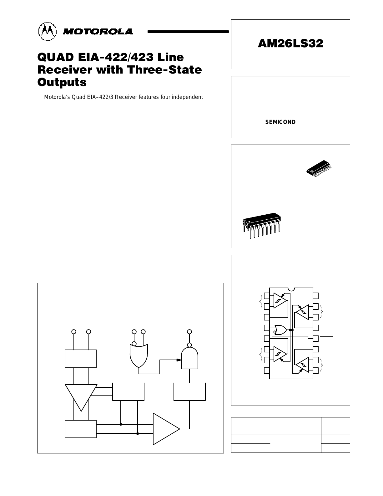
ORDERING INFORMATION
PIN CONNECTIONS
Order this document by AM26LS32/D
PC SUFFIX
PLASTIC PACKAGE
CASE 648
D SUFFIX
PLASTIC PACKAGE
CASE 751B
(SO–16)
Device
Operating
Temperature Range
Package
AM26LS32PC
MC26LS32D*
TA = 0 to 70°C
Plastic DIP
SO–16
9
–
+
–
8
7
6
5
4
3
2
1
10
11
12
13
14
+
–
+
–
Inputs A
+
V
CC
16
3–State
Control
GND
Output B
Output D
15
3–State
Control
Inputs C
Inputs B
Inputs D
Outputs A
Output C
1
MOTOROLA ANALOG IC DEVICE DATA
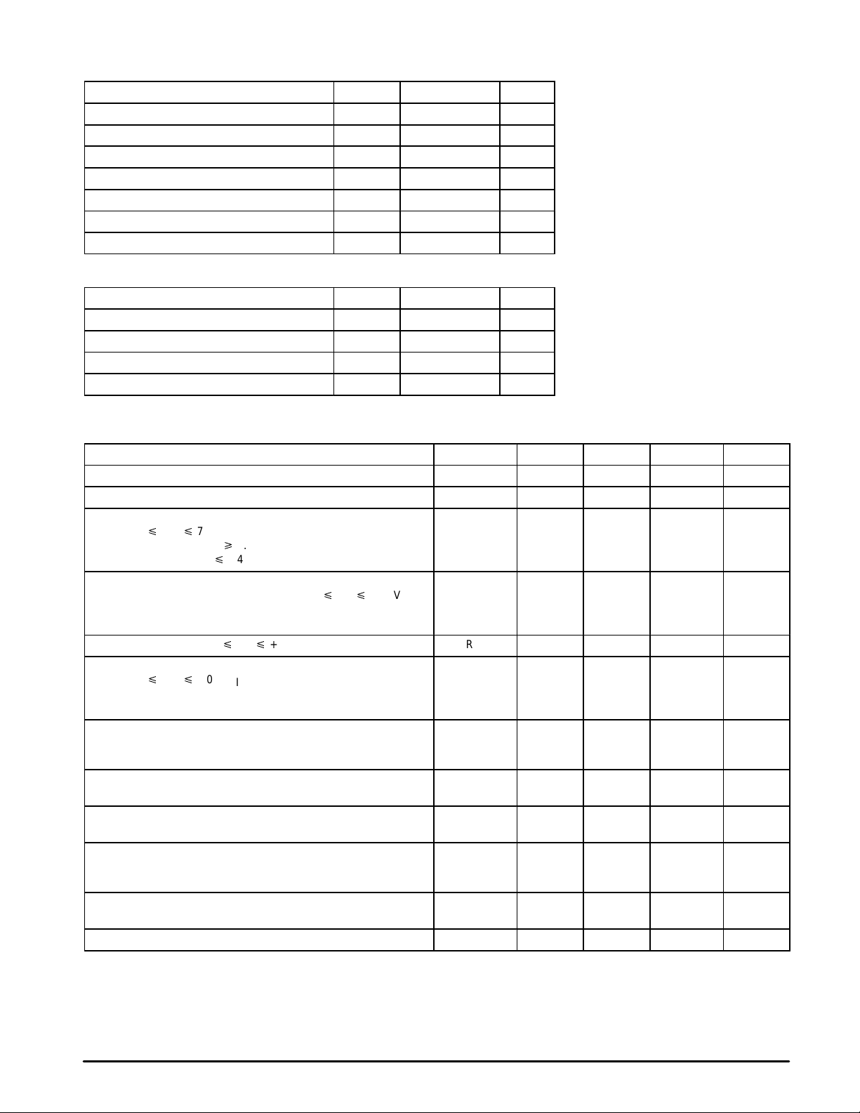
Motorola′s Quad EIA–422/3 Receiver features four independent receiver
chains which comply with EIA Standards for the Electrical Characteristics of
Balanced/Unbalanced Voltage Digital Interface Circuits. Receiver outputs
are 74LS compatible, three–state structures which are forced to a high
impedance state when Pin 4 is a Logic “0” and Pin 12 is a Logic “1.” A PNP
device buffers each output control pin to assure minimum loading for either
Logic “1” or Logic “0” inputs. In addition, each receiver chain has internal
hysteresis circuitry to improve noise margin and discourage output instability
for slowly changing input waveforms. A summary of AM26LS32 features
include:
• Four Independent Receiver Chains
• Three–State Outputs
• High Impedance Output Control Inputs
(PIA Compatible)
• Internal Hysteresis – 30 mV (Typical) @ Zero Volts Common Mode
• Fast Propagation Times – 25 ns (Typical)
• TTL Compatible
• Single 5.0 V Supply Voltage
• Fail–Safe Input–Output Relationship. Output Always High When Inputs
Are Open, Terminated or Shorted
• 6.0 k Minimum Input Impedance
* Note that the surface mount MC26LS32D device uses the same die as in the plastic DIP
* AM26LS32DC device, but with an MC prefix to prevent confusion with the package suffix.
Representative Block Diagram
Hysteresis
Amplifier
Amplifier
Three–State
Control
Inputs
Output
Differential
Inputs
Input
Network
Level
Translator
Level
Translator
Motorola, Inc. 1995
AM26LS32
2
MOTOROLA ANALOG IC DEVICE DATA
MAXIMUM RATINGS
Rating Symbol Value Unit
Power Supply Voltage V
CC
7.0 Vdc
Input Common Mode Voltage V
ICM
± 25 Vdc
Input Differential Voltage V
ID
± 25 Vdc
Three–State Control Input Voltage V
I
7.0 Vdc
Output Sink Current I
O
50 mA
Storage Temperature T
stg
– 65 to + 150 °C
Operating Junction Temperature T
J
+ 150 °C
RECOMMENDED OPERATING CONDITIONS
Rating Symbol Value Unit
Power Supply Voltage V
CC
4.75 to 5.25 Vdc
Operating Ambient Temperature T
A
0 to + 70 °C
Input Common Mode Voltage Range V
ICR
– 7.0 to + 7.0 Vdc
Input Differential Voltage Range V
IDR
6.0 Vdc
ELECTRICAL CHARACTERISTICS (Unless otherwise noted, minimum and maximum limits apply over recommended temperature
and power supply voltage ranges. Typical values are for TA = 25°C, VCC = 5.0 V and VIC = 0 V. See Note 1.)
Characteristic
Symbol Min Typ Max Unit
Input Voltage – High Logic State (Three–State Control) V
IH
2.0 – – V
Input Voltage – Low Logic State (Three–State Control) V
IL
– – 0.8 V
Differential Input Threshold Voltage (Note 2)
(–7.0 V p VIC p 7.0 V, VIH = 2.0 V)
(IO = –0.4 mA, VOH q 2.7 V)
(IO = 8.0 mA, VOL p 0.45 V)
V
TH(D)
–
–
–
–
0.2
–0.2
V
Input Bias Current
(VCC = 0 V or 5.25) (Other Inputs at –15 V p Vin p +15 V)
Vin = +15 V
Vin = –15 V
I
IB(D)
–
–
–
–
2.3
–2.8
mA
Input Resistance ( –15 V p Vin p +15 V) R
in
6.0 K – – Ohms
Input Balance and Output Level
(–7.0 V p VIC p 7.0 V, VIH = 2.0 V, See Note 3)
(IO = –0.4 mA, VID = 0.4 V)
(IO = 8.0 mA, VID = –0.4 V)
V
OH
V
OL
2.7
–
–
–
–
0.45
V
Output Third State Leakage Current
(V
I(D)
= + 3.0 V, VIL = 0.8 V, VO = 0.4 V)
(V
I(D)
= – 3.0 V, VIL = 0.8 V, VO = 2.4 V)
I
OZ
–
–
–
–
–20
20
µA
Output Short Circuit Current
(V
I(D)
= 3.0 V, VIH = 2.0 V, VO = 0 V, See Note 4)
I
OS
–15 – –85 mA
Input Current – Low Logic State (Three–State Control)
(VIL = 0.4 V)
I
IL
– – –360 µA
Input Current – High Logic State (Three–State Control)
(VIH = 2.7 V)
(VIH = 5.5 V)
I
IH
–
–
–
–
20
100
µA
Input Clamp Diode Voltage (Three–State Control)
(IIC = –18 mA)
V
IK
– – –1.5 V
Power Supply Current (VIL = 0 V) (All Inputs Grounded) I
CC
– – 70 mA
NOTES: 1.All currents into device pins are shown as positive, out of device pins are negative. All voltages referenced to ground unless otherwise noted.
2.Differential input threshold voltage and guaranteed output levels are done simultaneously for worst case.
3.Refer to EIA–422/3 for exact conditions. Input balance and guaranteed output levels are done simultaneously for worst case.
4.Only one output at a time should be shorted.
 Loading...