

SEMICONDUCTOR TECHNICAL DATA
4–356
REV 5
Motorola, Inc. 1996
3/93
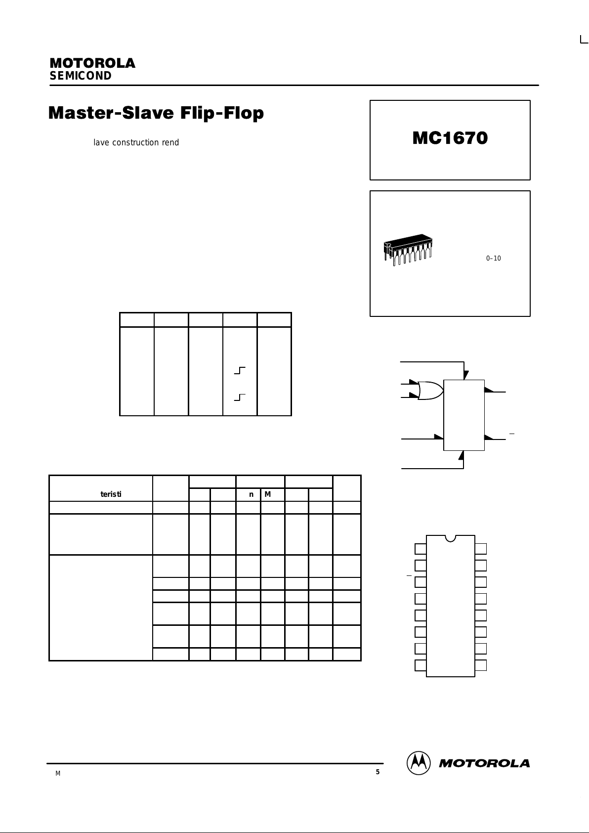
Master slave construction renders the MC1670 relatively insensitive to the
shape of the clock waveform, since only the voltage levels at the clock inputs
control the transfer of information from data input (D) to output.
When both clock inputs (C1 and C2) are in the low state, the data input
affects only the “Master” portion of the flip-flop. The data present in the “Master”
is transferred to the “Slave” when clock inputs (C1 “OR” C2) are taken from a
low to a high level. In other words, the output state of the flip-flop changes on the
positive transition of the clock pulse.
While either C1 “OR” C2 is in the high state, the “Master” (and data input) is
disabled.
Asynchronous Set (S) and Reset (R) override Clock (C) and Data (D) inputs.
Power Dissipation = 220 mW typ (No Load)
f
Tog
= 350 MHz typ
TRUTH TABLE
R S D C Q
n+1
L
H
H
L
L
L
L
L
L
H
L
H
L
L
L
L
L
L
X
X
X
L
L
L
H
H
H
X
X
X
L
H
H
L
H
L
N.D.
Q
n
L
Q
n
Q
n
H
Q
n
ND = Not Defined
C = C1 + C2
ELECTRICAL CHARACTERISTICS
–30°C +25°C +85°C
Characteristic Symbol
Min Max Min Max Min Max
Unit
Power Supply Drain Current I
E
— — — 48 — — mAdc
Input Current
Set, Reset
Clock
Data
I
inH
—
—
—
—
—
—
—
—
—
550
250
270
—
—
—
—
—
—
µAdc
Switching Times
Propagation Delay
t
pd
1.0 2.7 1.1 2.5 1.1 2.9
ns
Rise Time (10% to 90%) t
+
0.9 2.7 1.0 2.5 1.0 2.9 ns
Fall Time (10% to 90%) t
–
0.5 2.1 0.6 1.9 0.6 2.3 ns
Setup Time t
S“1”
t
S“0”
————0.4
0.5——————
ns
Hold Time t
H“1”
t
H“0”
————0.3
0.5——————
ns
Toggle Frequency f
Tog
270 — 300 — 270 — MHz
LOGIC DIAGRAM
S
C1
C2
D
R
Q
Q
V
CC1
= Pin 1
V
CC2
= Pin 16
VEE = Pin 8
PIN ASSIGNMENT
1
2
3
4
5
6
7
89
10
11
12
13
14
15
16V
CC1
Q
Q
RESET
SET
NC
V
EE
V
CC2
NC
NC
NC
NC
DATA
NC
CLOCK 2
CLOCK 1
5
7
9
11
4
2
3
L SUFFIX
CERAMIC PACKAGE
CASE 620–10
MC1670
4–357 MOTOROLAMECL Data
DL122 — Rev 6
+0.35
+0.3
TA = 25°C
VCC = +2.0 VDC
VEE = –3.2 VDC
F
TOG
(MHZ)
+0.25
+1.05
325275225175 375 425
+0.4
+0.45
+0.5
+0.65
+0.7
+0.75
+0.8
+0.85
+0.9
+0.95
+1.0
V
Bias
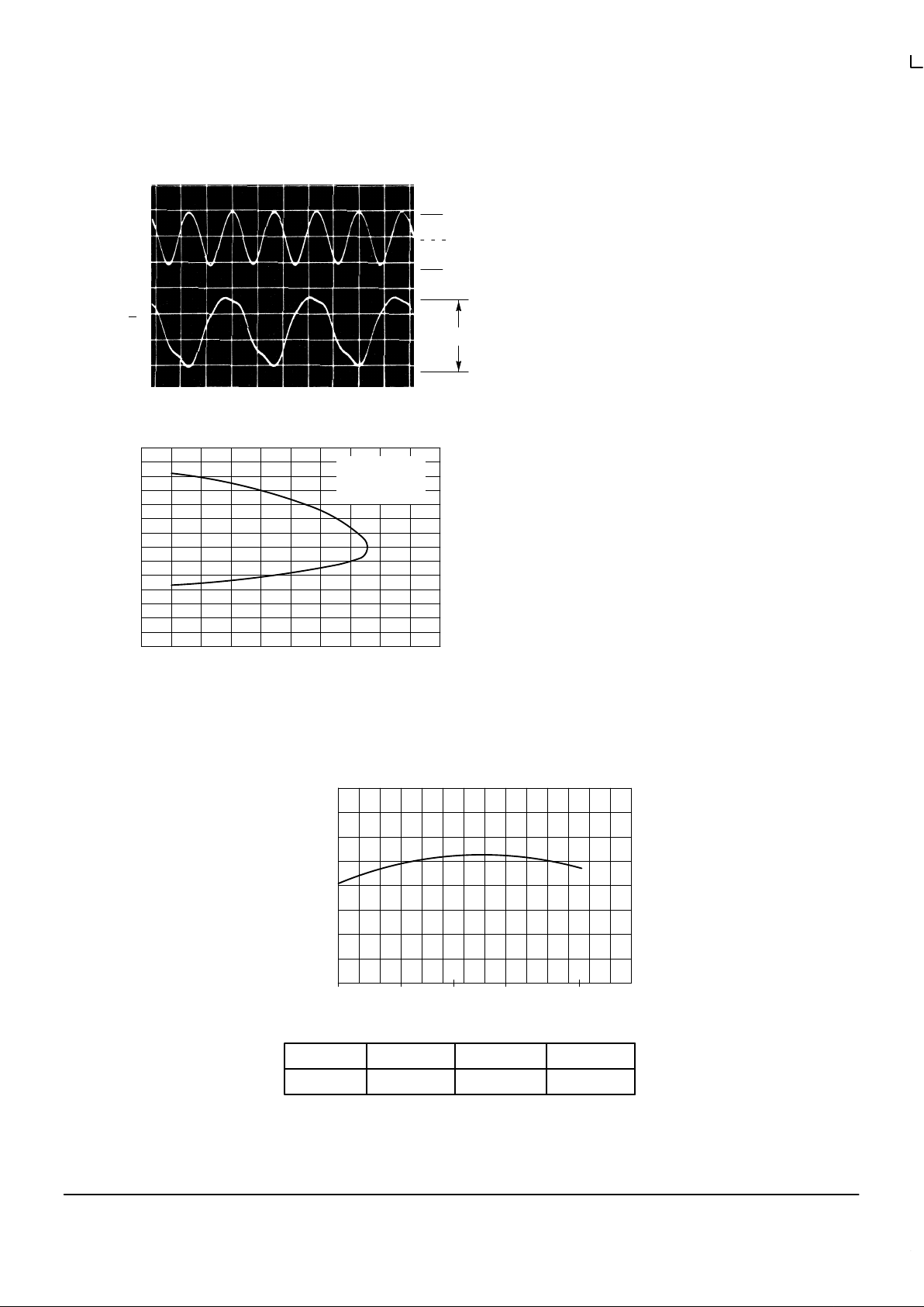
FIGURE 1 — TOGGLE FREQUENCY WAVEFORMS
TA = 25°C
+1.11 V
+0.71 V
BIAS
+0.31 V
600 MV MIN
The maximum toggle frequency of the MC1670 has been exceeded
when either:
1. The output peak-to-peak voltage swing falls below 600
millivolts,
OR
2. The device ceases to toggle (divide by two).
FIGURE 2 — MAXIMUM TOGGLE FREQUENCY (TYPICAL)
Figure 2 illustrates the variation in toggle frequency
with the dc offset voltage (V
Bias
) of the input clock signal.
Figures 4 and 5 illustrate minimum clock pulse width
recommended for reliable operation of the MC1670.
FIGURE 3 — TYPICAL MAXIMUM TOGGLE FREQUENCY
versus TEMPERA TURE
–30
250
TA, AMBIENT TEMPERATURE (
°
C)
300
02550 85
350
400
f , MAXIMUM TOGGLE
Tog max
FREQUENCY (MHz)
V
Bias
Temperature
+0.66 Vdc
–30°C
+0.71 Vdc
+25°C
+0.765 Vdc
+85°C
Note: All power supply and logic levels are shown shifted 2.0 volts positive.
CLOCK INPUT
300
MHZ-MAX
Q OR Q
OUTPUT

MC1670
MOTOROLA MECL Data
DL122 — Rev 6
4–358
FIGURE 4 — MINIMUM “DOWN TIME” TO CLOCK
OUTPUT LOAD = 50 Ω
FIGURE 5 — MINIMUM “UP TIME” TO CLOCK
OUTPUT LOAD = 50 Ω
Q OR
Q
CLOCK
1.0 NS/DIV .
1.0 NS/DIV .
Q OR
Q
CLOCK
SCALE
250 mV/DIV
SCALE
250 mV/DIV

MC1670
4–359 MOTOROLAMECL Data
DL122 — Rev 6
OUTLINE DIMENSIONS
L SUFFIX
CERAMIC DIP PACKAGE
CASE 620–10
ISSUE V
NOTES:
1. DIMENSIONING AND TOLERANCING PER
ANSI Y14.5M, 1982.
2. CONTROLLING DIMENSION: INCH.
3. DIMENSION L TO CENTER OF LEAD WHEN
FORMED PARALLEL.
4. DIMENSION F MAY NARROW TO 0.76 (0.030)
WHERE THE LEAD ENTERS THE CERAMIC
BODY.
–A–
–B–
–T–
F
E
G
N
K
C
SEATING
PLANE
16 PLD
S
A
M
0.25 (0.010) T
16 PLJ
S
B
M
0.25 (0.010) T
M
L
DIM MIN MAX MIN MAX
MILLIMETERSINCHES
A 0.750 0.785 19.05 19.93
B 0.240 0.295 6.10 7.49
C ––– 0.200 ––– 5.08
D 0.015 0.020 0.39 0.50
E 0.050 BSC 1.27 BSC
F 0.055 0.065 1.40 1.65
G 0.100 BSC 2.54 BSC
H 0.008 0.015 0.21 0.38
K 0.125 0.170 3.18 4.31
L 0.300 BSC 7.62 BSC
M 0 15 0 15
N 0.020 0.040 0.51 1.01
____
16 9
18
Motorola reserves the right to make changes without further notice to any products herein. Motorola makes no warranty , representation or guarantee regarding
the suitability of its products for any particular purpose, nor does Motorola assume any liability arising out of the application or use of any product or circuit, and
specifically disclaims any and all liability, including without limitation consequential or incidental damages. “T ypical” parameters which may be provided in Motorola
data sheets and/or specifications can and do vary in different applications and actual performance may vary over time. All operating parameters, including “Typicals”
must be validated for each customer application by customer’s technical experts. Motorola does not convey any license under its patent rights nor the rights of
others. Motorola products are not designed, intended, or authorized for use as components in systems intended for surgical implant into the body, or other
applications intended to support or sustain life, or for any other application in which the failure of the Motorola product could create a situation where personal injury
or death may occur. Should Buyer purchase or use Motorola products for any such unintended or unauthorized application, Buyer shall indemnify and hold Motorola
and its officers, employees, subsidiaries, affiliates, and distributors harmless against all claims, costs, damages, and expenses, and reasonable attorney fees
arising out of, directly or indirectly, any claim of personal injury or death associated with such unintended or unauthorized use, even if such claim alleges that
Motorola was negligent regarding the design or manufacture of the part. Motorola and are registered trademarks of Motorola, Inc. Motorola, Inc. is an Equal
Opportunity/Affirmative Action Employer.
How to reach us:
USA/EUROPE /Locations Not Listed: Motorola Literature Distribution; JAPAN: Nippon Motorola Ltd.; Tatsumi–SPD–JLDC, 6F Seibu–Butsuryu–Center,
P.O. Box 5405, Denver, Colorado 80217. 1–800–441–2447 3–14–2 Tatsumi Koto–Ku, Tokyo 135, Japan. 03–81–3521–8315
Mfax: RMFAX0@email.sps.mot.com – TOUCHT ONE 602–244–6609 ASIA/PACIFIC: Motorola Semiconductors H.K. Ltd.; 8B Tai Ping Industrial Park,
INTERNET: http://Design–NET.com 51 Ting Kok Road, Tai Po, N.T., Hong Kong. 852–26629298
MC1670/D
*MC1670/D*
◊
 Loading...