

SEMICONDUCTOR TECHNICAL DATA
4–334
REV 5
Motorola, Inc. 1996
3/93
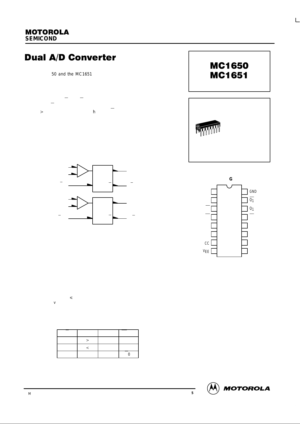
The MC1650 and the MC1651 are very high speed comparators utilizing
differential amplifier inputs to sense analog signals above or below a reference
level. An output latch provides a unique sample-hold feature. The MC1650
provides high impedance Darlington inputs, while the MC1651 is a lower
impedance option, with higher input slew rate and higher speed capability.
The clock inputs (C
a
and Cb) operate from MECL III or MECL 10,000 digital
levels. When C
a
is at a logic high level, Q0 will be at a logic high level provided
that V1 u V2 (V1 is more positive than V2). Q
0 is the logic complement of Q0.
When the clock input goes to a low logic level, the outputs are latched in their
present state.
Assessment of the performance differences between the MC1650 and the
MC1651 may be based upon the relative behaviors shown in Figures 4 and 7.
• PD= 330 mW typ/pkg (No Load)
• tpd= 3.5 ns typ (MC1650)
= 3.0 ns typ (MC1651)
• Input Slew Rate = 350 V/µs (MC1650)
= 500 V/µs (MC1651)
• Differential Input Voltage: 5.0 V (–30°C to +85° C)
• Common Mode Range:
–3.0 V to +2.5 V (–30°C to +85°C) (MC1651)
–2.5 V to +3.0 V (–30°C to +85°C) (MC1650)
• Resolution: p 20 mV (–30°C to +85°C)
• Drives 50 Ω lines
Number at end of terminal denotes pin number for L package (Case 620).
LOGIC DIAGRAM
+
–
+
–
V1A 6
V2A 5
C
A
4
V1B 12
V2B 11
C
B
13
2 Q0
3 Q
0
14 Q1
15 Q
1
VCC= +5.0 V = PIN 7, 10
VEE= –5.2 V = PIN 8
GND = PIN 1, 16
DQ
Q
D
Q
Q
TRUTH TABLE
C V1 , V2Q0n + 1Q0n +
1
HV1 u
V
2
HL
HV1 t
V
2
LH
L X X Q0
n
Q0
n
PIN ASSIGNMENT
GND
Q
0
Q
0
C
A
V
2A
V
1A
V
CC
V
EE
GND
Q
1
Q
1
C
B
V
1B
V
2B
V
CC
NC
1
2
3
4
5
6
7
8
16
15
14
13
12
11
10
9
L SUFFIX
CERAMIC PACKAGE
CASE 620–10
MC1650 MC1651
4–335 MOTOROLAMECL Data
DL122 — Rev 6
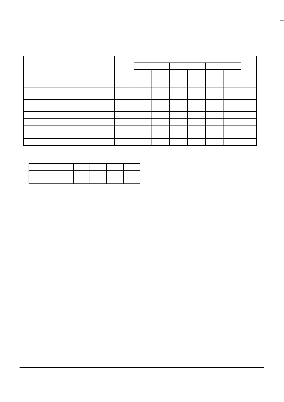
ELECTRICAL CHARACTERISTICS
Test Limits
–30°C +25°C +85°C
Characteristic Symbol
Min Max Min Max Min Max
Unit
Power Supply Drain Current Positive
Negative
I
CC
I
E
25*
55*
mAdc
Input Current MC1650
MC1651
I
in
10
40
µAdc
Input Leakage Current MC1650
MC1651
I
R
7.0
10.0
µAdc
Clock Input Current I
inH
350
Output Voltage Logic 1 V
OH
–1.045 –0.875 –0.960 –0.810 –0.890 –0.700 Vdc
Output Voltage Logic 0 V
OL
–1.890 –1.650 –1.850 –1.620 –1.830 –1.575 Vdc
Threshold Voltage (Note 2.) Logic 1 V
OHA
–1.065 –0.980 –0.910 Vdc
Threshold Voltage (Note 2.) Logic 0 V
OLA
–1.630 –1.600 –1.555 Vdc
1. All data is for 1/2 MC1650 or MC1651, except data marked (*) which refers to the entire package.
2. These tests are done in order indicated. See Figure 5.
3. Maximum Power Supply Voltages (beyond which device life may be impaired): |VEE| + |VCC| ≥ 12 Vdc.
4. All Temperature
V
A3
V
A4
V
A5
V
A6
MC1650 +3.0 +2.98 –2.5 –2.48
MC1651 +2.5 +2.48 –3.0 –2.98
MC1650 MC1651
MOTOROLA MECL Data
DL122 — Rev 6
4–336
ELECTRICAL CHARACTERISTICS (continued)
TEST VOLTAGE VALUES (Volts)
@ Test Temperature
V
IHmaxVILminVIHAminVILAmaxVA1VA2VA3VA4VA5VA6VCC
3.
V
EE
3.
–30°C –0.875 –1.890 –1.180 –1.515 +0.02 +0.02
+5.0 –5.2
+25°C –0.810 –1.850 –1.095 –1.485 +0.02 +0.02
See Note 4.
+5.0 –5.2
+85°C –0.700 –1.830 –1.025 –1.440 +0.02 +0.02 +5.0 –5.2
TEST VOLTAGE APPLIED TO PINS LISTED BELOW
Characteristic Symbol
V
IHmaxVILminVIHAminVILAmaxVA1VA2VA3VA4VA5VA6
(VCC)
Gnd
Power Supply Pos
Drain Current Neg
I
CC
I
E
4,13
4,13 6,12
6,12
1,5,11,16
1,5,11,16
Input Current MC1650
MC1651
I
in
4 13 12 6 1,5,11,16
Input Leakage MC1650
Current MC1651
I
R
4 13 12 6 1,5,11,16
Clock Input Current I
inH
4 13 6,12 1,5,11,16
Output Voltage Logic 1 V
OH
4,13 6,12
5,11
5,11
6,12
6,12
5,11
5,11
6,12
5,11
6,12
6,12
5,11
1,5,11,16
1,6,12,16
1,16
1,16
1,5,11,16
1,6,12,16
1,16
1,16
Output Voltage Logic 0 V
OL
4,13
5,11
6,12
6,12
5,11
5,11
6,12
6,12
5,11
6,12
5,11
5,11
6,12
1,5,11,16
1,6,12,16
1,16
1,16
1,5,11,16
1,6,12,16
1,16
1,16
Threshold Logic 1
Voltage
Note 2.
V
OHA
13 4
4
4
4
6
6
6
6
1,5,16
Threshold Logic 0
Voltage
Note 2.
V
OLA
13 4
4
4
4
6
6
6
6
1,5,16
1. All data is for 1/2 MC1650 or MC1651, except data marked (*) which refers to the entire package.
2. These tests are done in order indicated. See Figure 5.
3. Maximum Power Supply Voltages (beyond which device life may be impaired): |VEE| + |VCC| ≥ 12 Vdc.
4. All Temperature
V
A3
V
A4
V
A5
V
A6
MC1650 +3.0 +2.98 –2.5 –2.48
MC1651 +2.5 +2.48 –3.0 –2.98
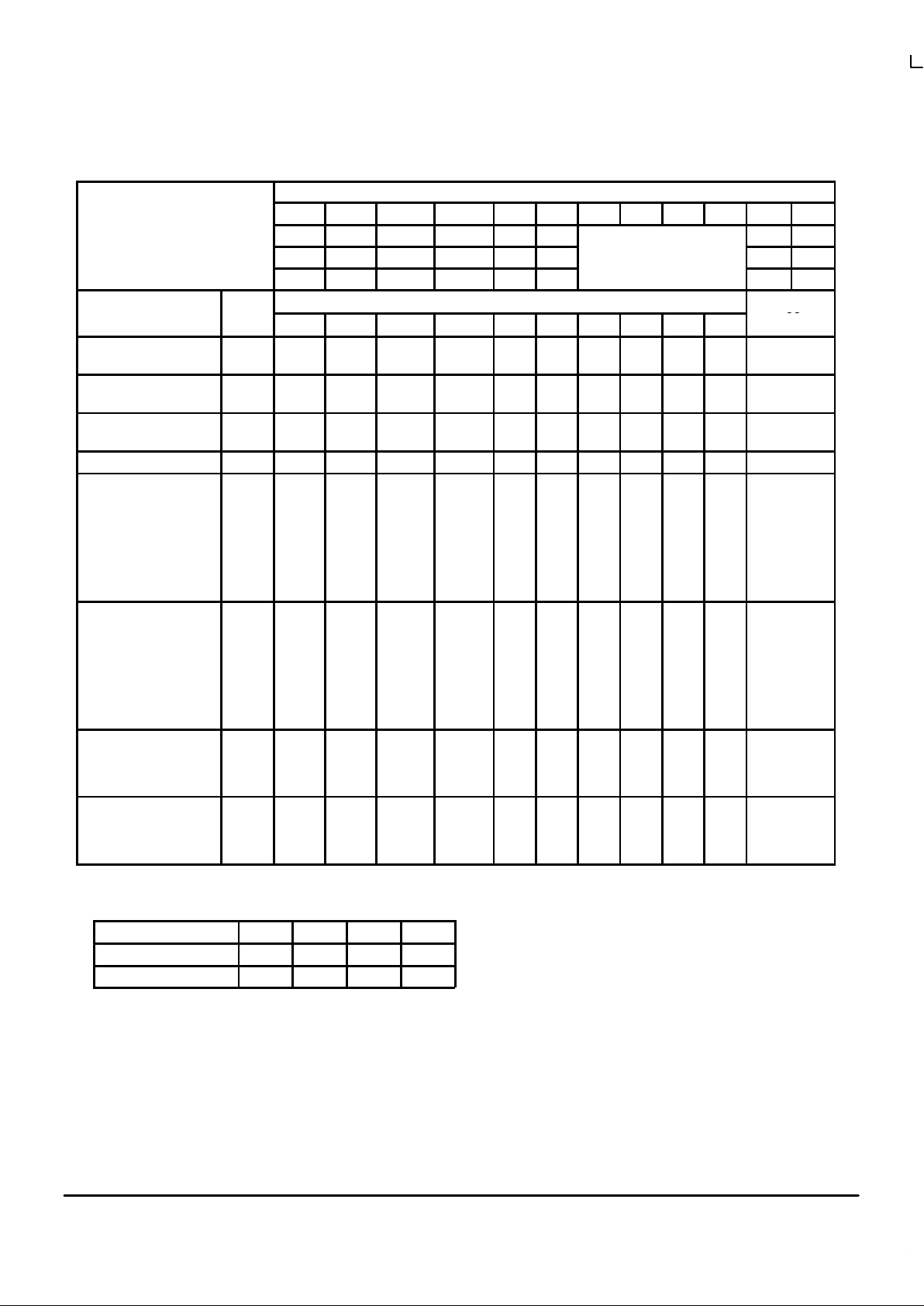
Each MECL 10,000 series circuit has been designed to meet the dc specifications shown in the test table, after thermal equilibrium has been
established. The circuit is in a test socket or mounted on a printed circuit board and transverse air flow greater than 500 linear fpm is maintained.
Outputs are terminated through a 50–ohm resistor to –2.0 volts. Test procedures are shown for only one gate. The other gates are tested in the
same manner.
MC1650 MC1651
4–337 MOTOROLAMECL Data
DL122 — Rev 6
MC1651 Inputs
V
CC
7, 10
Gnd
1
Gnd
16
A
B
C
2 Q
3 Q
4
Clock
R
P
8 V
EE
D
E
(Both Devices)
A
B
C
D
E
V1 6
V2 5
MC1650 Inputs
A
B
C
V1 6
V2 5
D
E
CIRCUIT SCHEMATIC
1/2 of Device Shown
SWITCHING TEST VOLTAGE VALUES
@Test
(Volts)
@Test
Temperature
V
R1
V
R2
V
R3
V
X
V
XX
V
CC
1
V
EE
1
–30°C +2.0
+1.04 +2.0 +7.0 –3.2
+25°C +2.0
See Note 4
+1.11 +2.0 +7.0 –3.2
+85°C +2.0 +1.19 +2.0 +7.0 –3.2
–30°C +25°C +85°C
Conditions
Characteristic Symbol
Min Max Min Max Min Max
Unit
Conditions
(See Figures 1–3)
Switching Times
Propagation Delay
(50% to 50%) V-Input
t
pd
2.0 5.0 2.0 5.0 2.0 5.7
ns
VR1 to V2, VX to Clock, P1 to V1, or,
VR2 to V2, VX to Clock, P2 to V1, or,
VR3 to V2, VX to Clock, P3 to V1.
Clock
2
2.0 4.7 2.0 4.7 2.0 5.2 VR1 to V2, P1 to V1 and P4 to Clock,
or, VR1 to V1, P1 to V2 and P4 to Clock.
Clock Enable
3
t
setup
— — 2.5 — — — ns
Clock Aperture
3
t
ap
— — 1.5 — — — ns
V
R1
to
V
2
,
P
1
to
V
1
,
P
4
to Cloc
k
Rise Time (10% to 90%)
t
+ 1.0 3.5 1.0 3.5 1.0 3.8 ns
Fall Time (10% to 90%)
t
–
1.0 3.0 1.0 3.0 1.0 3.3 ns
VR to V2, VX to Clock, P1 to V1.
NOTES:
1. Maximum Power Supply Voltages (beyond which device life
may be impaired:
VCC + VEE q 12 Vdc.
2. Unused clock inputs may be tied to ground.
3. See Figure 3.
All Temperatures
V
R2
MC1650 +4.9
MC1651 +4.4
V
R3
–0.4
–0.9
4.
 Loading...