

Motorola MC1488D, MC1488P Datasheet
T
0 to
75°C
The MC1488 is a monolithic quad line driver designed to interface data
terminal equipment with data communications equipment in conformance
with the specifications of EIA Standard No. EIA–232D.
Features:
• Current Limited Output
±10 mA typical
• Power–Off Source Impedance
300 Ω mininum
• Simple Slew Rate Control with External Capacitor
• Flexible Operating Supply Range
• Compatible with All Motorola MDTL and MTTL Logic Families
ORDERING INFORMATION
Operating
Device
MC1488P
MC1488D
Temperature Range
°
+
=
A
Package
Plastic
SO–14
Order this document by MC1488/D
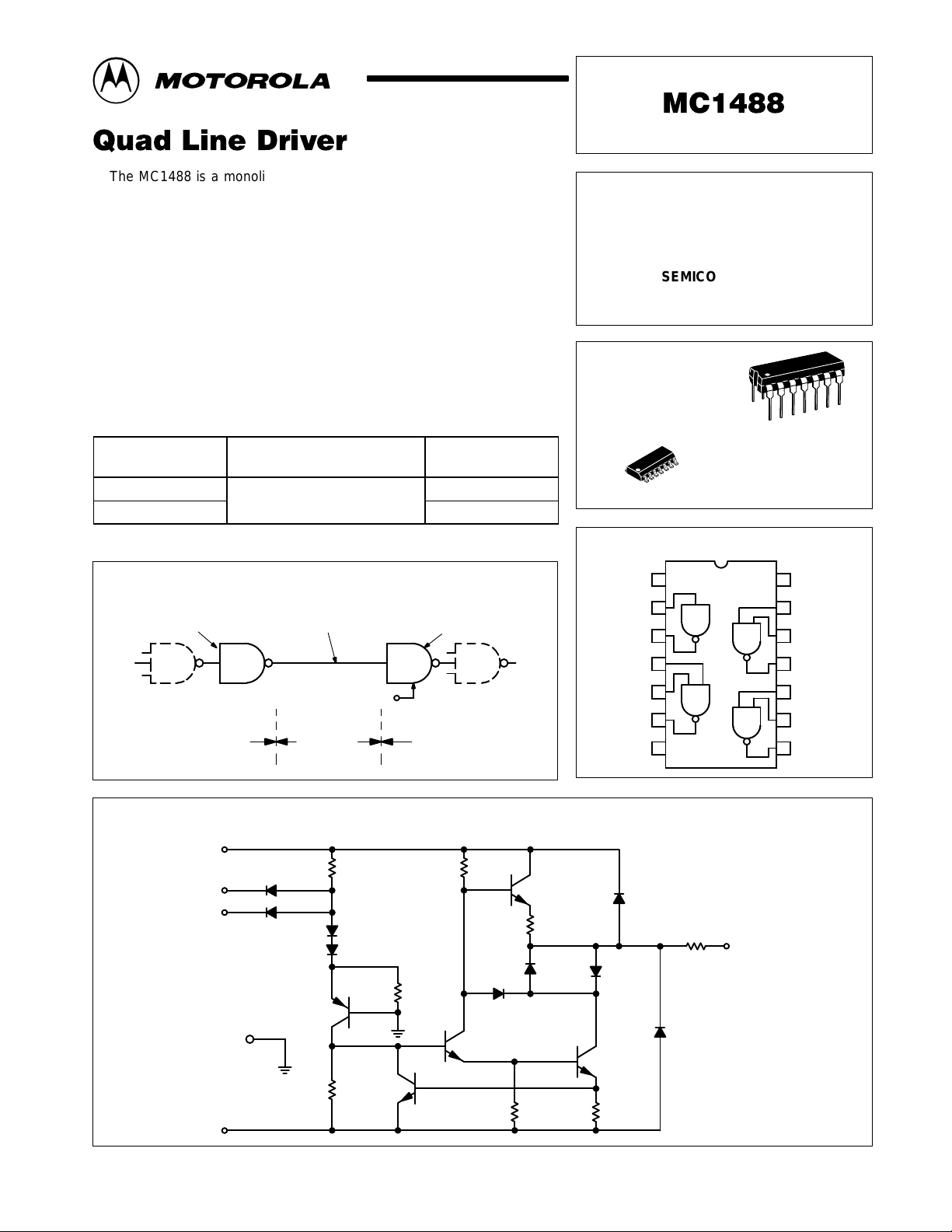
QUAD MDTL LINE DRIVER
EIA–232D
SEMICONDUCTOR
TECHNICAL DATA
P SUFFIX
PLASTIC PACKAGE
CASE 646
D SUFFIX
PLASTIC PACKAGE
CASE 751A
(SO–14)
Line Driver
MC1488
MDTL Logic Input
VCC 14
Pins 4, 9, 12 or 2
Input
Input
Pins 5, 10, 13
Simplified Application
Interconnecting
Cable
Interconnecting
Cable
8.2 k
Line Receiver
MC1489
MDTL Logic Output
Circuit Schematic
(1/4 of Circuit Shown)
6.2 k
3.6 k
PIN CONNECTIONS
1
V
EE
2
Input A
3
Output A
4
Input B1
5
Input B2
6
Output B
7
Gnd
70
300
Pins 6, 8, 11 or 3
Output
14
V
Input D1
13
Input D2
12
Output D
11
Input C1
10
Input C2
9
Output C
8
CC
GND 7
10 k
7.0 k 70
VEE 1
Motorola, Inc. 1996 Rev 3
MOTOROLA ANALOG IC DEVICE DATA
1
MC1488
MAXIMUM RATINGS (T
Power Supply Voltage V
Input Voltage Range V
Output Signal Voltage V
Power Derating (Package Limitation, SO–14
and Plastic Dual–In–Line Package)
Derate above TA = + 25°C
Operating Ambient Temperature Range T
Storage Temperature Range T
ELECTRICAL CHARACTERISTICS (V
Input Current – Low Logic State (VIL = 0) I
Input Current – High Logic State (VIH = 5.0 V) I
Output Voltage – High Logic State
(VIL = 0.8 Vdc, RL = 3.0 kΩ, VCC = + 9.0 Vdc, VEE = – 9.0 Vdc)
(VIL = 0.8 Vdc, RL = 3.0 kΩ, VCC = + 13.2 Vdc, VEE = – 13.2 Vdc)
Output Voltage – Low Logic State
(VIH = 1.9 Vdc, RL = 3.0 kΩ, VCC = + 9.0 Vdc, VEE = – 9.0 Vdc)
(VIH = 1.9 Vdc, RL = 3.0 kΩ, VCC = + 13.2 Vdc, VEE = – 13.2 Vdc)
Positive Output Short–Circuit Current, Note 1 I
Negative Output Short–Circuit Current, Note 1 I
Output Resistance (VCC = VEE = 0, VO = ± 2.0 V) r
Positive Supply Current (RI = ∞)
(VIH = 1.9 Vdc, VCC = + 9.0 Vdc)
(VIL = 0.8 Vdc, VCC = + 9.0 Vdc)
(VIH = 1.9 Vdc, VCC = + 12 Vdc)
(VIL = 0.8 Vdc, VCC = + 12 Vdc)
(VIH = 1.9 Vdc, VCC = + 15 Vdc)
(VIL = 0.8 Vdc, VCC = + 15 Vdc)
Negative Supply Current (RL = ∞)
(VIH = 1.9 Vdc, VEE = – 9.0 Vdc)
(VIL = 0.8 Vdc, VEE = – 9.0 Vdc)
(VIH = 1.9 Vdc, VEE = – 12 Vdc)
(VIL = 0.8 Vdc, VEE = – 12 Vdc)
(VIH = 1.9 Vdc, VEE = – 15 Vdc)
(VIL = 0.8 Vdc, VEE = – 15 Vdc)
Power Consumption
(VCC = 9.0 Vdc, VEE = – 9.0 Vdc)
(VCC = 12 Vdc, VEE = – 12 Vdc)
= +25°C, unless otherwise noted.)
A
Rating Symbol Value Unit
+ 15
– 15
– 15 p VIR
7.0
±15 Vdc
1000
6.7
0 to + 75 °C
– 65 to + 175 °C
Characteristic
CC
V
EE
IR
O
P
D
1/R
θJA
A
stg
= + 9.0 ± 1% Vdc, VEE = –9.0 ± 1% Vdc, TA = 0 to 75°C, unless otherwise noted.)
CC
Vdc
p
Vdc
mW
mW/°C
Symbol Min Typ Max Unit
IL
IH
V
OH
V
OL
OS+
OS–
o
I
CC
I
EE
P
C
– 1.0 1.6 mA
– – 10 µA
+ 6.0
+ 9.0
– 6.0
– 9.0
+ 6.0 + 10 + 12 mA
– 6.0 – 10 – 12 mA
300 – – Ohms
–
–
–
–
–
–
–
–
–
–
–
–
–
–
+7.0
+10.5
– 7.0
– 10.5
+ 15
+ 4.5
+ 19
+ 5.5
–
–
– 13
–
– 18
–
–
–
–
–
–
–
–
–
+ 20
+ 6.0
+ 25
+ 7.0
+ 34
+ 12
– 17
– 500
– 23
– 500
– 34
– 2.5
333
576
Vdc
Vdc
mA
mA
µA
mA
µA
mA
mA
mW
SWITCHING CHARACTERISTICS (V
Propagation Delay Time (zI = 3.0 k and 15 pF) t
Fall Time (zI = 3.0 k and 15 pF) t
Propagation Delay Time (zI = 3.0 k and 15 pF) t
Rise Time (zI = 3.0 k and 15 pF) t
NOTE: 1. Maximum Package Power Dissipation may be exceeded if all outputs are shorted simultaneously.
= +9.0 ± 1% Vdc, VEE = –9.0 ± 1% Vdc, TA = +25°C.)
CC
PLH
THL
PHL
TLH
2
– 275 350 ns
– 45 75 ns
– 110 175 ns
– 55 100 ns
MOTOROLA ANALOG IC DEVICE DATA
MC1488
CHARACTERISTIC DEFINITIONS
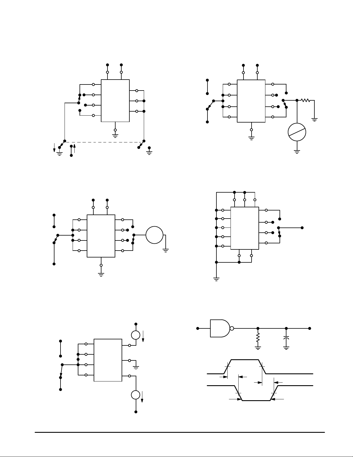
Figure 1. Input Current Figure 2. Output Voltage
–9.0 V
9.0 V
1
14
1.9 V
9.0 V
14 1
–9.0 V
2
4
9
12
7
I
IL
I
IH
5.0 V
5
V
10
13
OL
V
OH
0.8 V
2
4
9
12
7
Figure 3. Output Short–Circuit Current Figure 4. Output Resistance (Power Off)
V
V
EE
I
OS+
I
OS–
1.9 V
CC
14
1
2
2
4
9
12
3
6
8
11
I
OS
±
4
5
9
10
7
14
1
3
6
8
11
12
13
3
V
OH
V
OL
±
2.0 Vdc
±
6.6 mA Max
3.0 k
V
O
6
8
11
0.8 V
7
Figure 5. Power Supply Currents Figure 6. Switching Response
V
CC
e
1.9 V
2
V
IH
V
IL
0.8 V
4
9
12
I
CC
14
7
1
I
EE
V
EE
in
3.0 V
1.5 V
e
in
V
O
t
THL
t
PHL
t
THL
50%
and t
Measured 10% to 90%
TLH
t
PLH
t
TLH
V
O
15 pF3.0 k
0 V
MOTOROLA ANALOG IC DEVICE DATA
3
 Loading...