

Motorola MC146818, MC146818AL, MC146818AP, MC146818C Datasheet
I
Advance Information
I I
REAL-TIME CLOCK PLUS RAM (RTC)
The MC146818A Real-Time Clock plus RAM is a peripheral device
which includes the unique MOTEL concept for use with various
microprocessors, microcomputers, and larger computers. This part
combines three unique features: a complete time-of-day clock with
alarm and one hundred year calendar, a programmable periodic interrupt and square-wave generator, and 50 bytes of low-power static
RAM. The MC146818A uses high-speed CMOS technology to interface
with 1 MHz processor buses, while consuming very little power.
The Real-Time Clock plus RAM has two distinct uses. First, it is
designed as a battery powered CMOS part (in an otherwise NMOS/TTL
system) including all the common battery backed-up functions such as
RAM, time, and calendar. Secondly, the MC146818A maybe used with
a CMOS microprocessor to relieve the software of the timekeeping ,~~
workload and to extend the available RAM of an MPU such as the ., “’~:$
MC146805E2.
,!!:\’;
.\,i,.,..
. ....
● Low-Power, High-Speed CMOS
~\}t
,.,.>*t!F\+{k
,1,
$s,,..
● Internal Time Base and Oscillator
~;, ~p
)>.
~$$~.
‘,&Q.%~!*
O Counts Seconds, Minutes, and Hours of the Day
*>sq,.,,\,$4:*,
$+.~:;;,. ..~.
“’t:>?,.
● Counts Days of the Week, Date, Month, and Year ,$:
;<4 ,
● 3 V to 6 V Operation
..!.*:,:
~t.k,$,.,
● Time Base Input Options: 4.194304 MHz, 1.048ti ~~z, or 32.7W
kHz
,,,,,,M,,)$f,
<..%.-...*<.*$,
,$\ \.,
,,:,,
. ..i,;t~
● Time Base Oscillator for Parallel Resonan~$$~{S]s
.~;\l...
● 40 to 200 pW Typical Operating Power{,~L:~#~ ‘Frequency Time Base
● 4.0 to 20 mW Typical Operating Po.~%j~*$?gh Frequency Time Base
,~$.~,,,
● Binary or BCD Representation ~fTW~ Calendar, and Alarm
● 12- or 24-Hour Clock with A~$oQ$PM in 12-Hour Mode
.$k,..?.l,{+<,,$$,>:,.,
● Daylight Savings Time OplWn ‘$
*;* $*,,$$
● Automatic End of Mo~:~’’~$e6gnition
● Automatic Leap Y~r ~&&~ensation
● Microprocessor#$@t@mpatible
~‘.$$*$
● Selectable Ba$W&n’Wotorola and Competitor Bus Timing
, -~.,y,}$~*
● Multiplex@:~@ fbr Pin Efficiency
~’.,-,,
● lnterfq&$&%@% Software as 64 RAM Locations
● 14 B~es:$’~CIOck and Control Registers
,,*J
● ~’~~~~$i’of General Purpose RAM
....~.
@x;.$J&%wsBit indicates Data Integrity
?{&us Compatible Interrupt Signals (~Q)
..
● Three Interrupts are Separately Software Maskable and Testable
Time-of-Day Alarm, Once-per-Second to Once-per-Day
Periodic Rates from 30.5 ps to 500 ms
End-of-Clock Update Cycle
● Programmable Square-Wave Output Signal
● Clock Output May Be Used as Microprocessor Clock Input
At Time Base Frequency -1 or +4
● 24-Pin Dual-In-Line Package
● Quad Pack Also Available
.
hls document contains !ntormatlon on a new product. Specltlcatlons and tntormatlon here!n
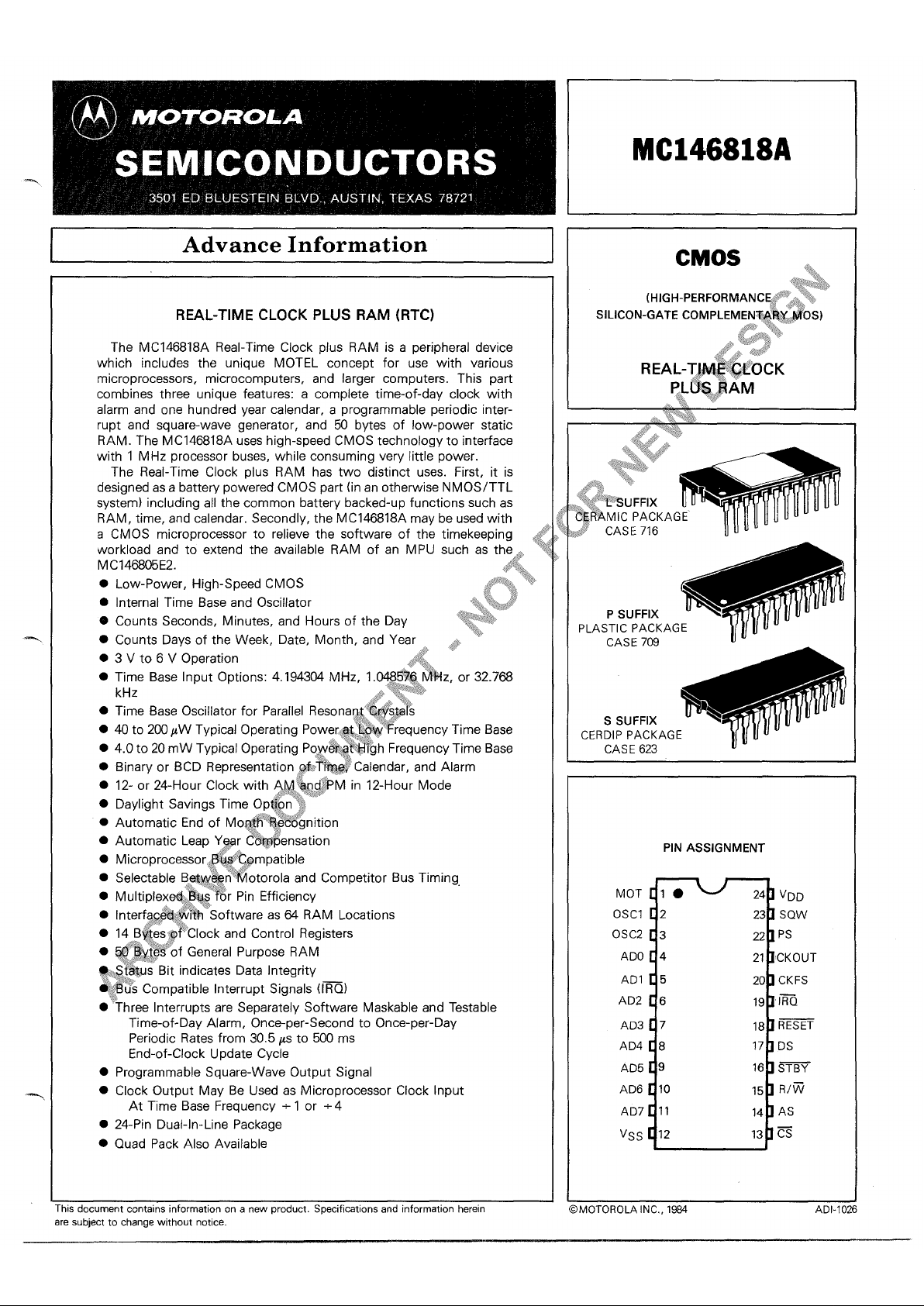
MC146818A
CMOS \
CASE 623
u“
I
PIN ASSIGNMENT
‘oT ~vDD
Oscl [ 2
23 ] SQW
0SC2 [ 3 22 ] Ps
ADO [ 4
21 JCKOUT
AD1 [ 5
20 ] CKFS
AD2 [ 6
lg ] l~Q
AD3 [ 7
18 ] RESET
AD4 [ 8
17 ] DS
AD5 c g
16 ] STBY
AD6 [ 10
15 ] Rl~
AD7 [ 11 14 ] AS
Vss [
12
13 ]=
)MOTOROLAINC,, lW
ADI-1026
are subject to change without notice
FIGURE 1 – BLOCK DIAGRAM
Clock
~ CKOUT
+
output
~ CKFS
v
Storage Temperature Range
Tstg
–55to +150
Oc
THERMAL CHARACTERISTICS
Characteristic
Symbol I
Value Unit
User RAM
(50 Bytes)
sow
~Q
RESET
Ps
,i,>,~
.. ~><.,
,*
.*$:, \ h .
~:*.
. ..
?+
$.;).,,<,:?
,’<;}.:-
MAXIMUM RATINQ~~(@oJjages referenced to VSS)
R~$n& “~:?’
Symbol Value
Unit
Supply Volta~J** “ ‘$?
VDD –0.3 to +8.0
v
All Input V:$~&.~xcept OSC1
Vin V5S– O.5 to VDD+O.5
v
Current ~rai~~r Pin Excluding
Vmi,a%q,.vs s
I 10
mA
This device contains circuitry to protect the in-
Op&~~~&Temperature Range
puts against damage due to high static voltages
TL to TH
or electric fields; however, it is advised that nor-
‘~%$~6818A
0 to 70
‘<@c146818AC
mal precautions be taken to avoid application of
TA
– 40 to 85
Oc
any voltage higher than maximum rated voltages
to this high-impedance circuit. For proper operation it is recommended that Vin and Vout be constrained to the range VSS =(Vin or Voutl
s VDD. Reliability of operation is enhanced if
unused inputs are tied to an appropriate logic
voltage level (e.g., either VSS or VDD).
Thermal Resistance
Plastic
I I
120
I I
Cerdlp 9JA
65 “c/w
Ceramic
50
@
MOTOROLA Semiconductor Products Inc.
2
—
—
)C ELECTRICAL CHARACTERISTICS (vD
D= 3
Vdc, vs s = O Vdc, TA = Tl to TH unless otherwise noted)
Characteristics
I Symbol I Min
I
Max
I
Unit
I
Frequency of Operation
fosc
32.768 32.768
kHz
Output Voltage vOL
—
0.1
lLoad< lOpA vOH
v
VDD– O.1 –
IDD – Bus Idle
CKOUT=fosc, CL= 15 pF; SOW Disabled, STBY=O.2 V; CL (OSC2)= 10 pF
fosc=32.76B kHz
.\,
IDD3 –
50
A&fi%$k
IDD – Quiescent
IDD4 –
50
“~{?.
fosc= DC; OSC1 = DC;
$“’:#$, !,
~~.+,,~i:”
All Other
lnpUtS=vDD–0.2 V;
:,.:,.~
~+,,....
. .:s.‘ ..
NO Clock
i,,..
..,t>.$.‘:.*$
\k;~#\ ~,
....,.
Output High Voltege
.,+ ..%)$
i’t” *
(lLoad= – 0.25 mA, All Outputs)
~-.>,,->,,.,/,
vOH
2.7 t+?’+’~’’t;;k~ v
Output Low Voltage
?J
<t~tl,
(iLoad= 0.25 mA, All
OUtpUtS)
,,} \k*t
VOL
$i.,,,,
-$.*;,,’:,: ~
0.3 v
Input High Voltage
——
STBY, ADO-AD7, DS, AS, R/W, CS
vlH
, %&$$y’
VDD v
RESET, CKFS, PS, OSC1
.,$,@,q.,
VDD
‘$:?y$:~ ~?:,
MOT
,,. ‘k$,’w.~’D
VDD
Input Low Voltage
——
~, ADO-AD7, DS, AS, R/W, CS, CKFS, PS, RESET, OSCI
vlL ‘?$yvss
0.5 v
MOT .#vj
Vss
Vss
Input Current
AS, DS, R/~F
~~:$~
–
* 10
—— —
PA
MOT, OSCI, CE, STBY, RESET, CKFS, ,P# ‘$ ‘“
*I
Three-State Leakage IRQ, AD@@fl~lTsL –
* 10 WA
.::.
Input Current
AS, DS, R/~
Iin
I I
+10 AA
—— —
MOT, OSCI, CE, STBY, RESET, CKFS, PS
—
*1
I
1 1
, I
Three-State Leakage IRQ, ADO-AD7 ITSL I –
*IO
PA
1
m
MOTOROkA Semiconductor Products Inc.
3
BUS TIMING
VDD=5.O V
*lo%
Vnn=3.O V
1 TTL and
Ident.
ti;F Load
130 pF Load
Number
Characteristi~ Symbol
Min Max Min Max Unit
1 Cycle Time
tcvc
5000 –
953 dc
ns
2 Pulse Width, DS/E Low or ~D/WR High PWEL lm
—
300 –
ns
3——Pulse Width, DS/E High or RD/WR Low PWEH 15m
—
325 –
ns
4 Input Rise and Fall Time tr, tf
—
100
—
30
ns
8 R/~ Hold Time tRWH 10 – 10 – ns “~$
13 R/~ Setup Time Before DS/E
,:,,,
tRWS 2m –
80
*.#*..,...,:{
—
~s %+.<
.$..
14 Chip Select Setup Time Before DS, ~R, or ~D tcs
200 –
,,.
25
—
~: m
15
Chip Select Hold Time
tCH 10
—
o
—
,,~r$
~~~;~e.:
18 Read Data Hold Time tDHR 10
Im
10
21 Write Data Hold Time
tnu\A/ 100 – o
SI24
Muxed Address Valid Time to AS/ALE Fall
I
tASL 2~ –
I
50 ,~p+:;a “’
I
n:
25 I Muxed Address Hold Time tAHL 100 I –
w “t “-
~*... ..s..’
~y>>,
ns
I
—
26
DelaV Time DS/E to AS/ALE Rise
tASD m –
, ‘* ‘ .- ns
27 Pulse Width, AS/ALE High
pwAs H
6~
– *,i$
;~J$$95
—
ns
28
DelaV Time, AS/ALE to DS/E Rise
tASED 500
* %:.\tf.,:/?@
ax..,.!>.
—
ns
30
Peripheral Output Data Delay Time from DS/ E or ~ tDDR 1300
.,~.,.,.?~...‘,’!..~,~
‘.?.?~i~,.~,:,
20 240
ns
31
Peripheral Data Setup Time tDSW 1q$.ii ~. ~’ 2m – ns
32
S~ Setup Time before AS/ALE Rise
tSBS
~Q:@:J~$+’3’–
TBD –
33
S~ Hold Time after AS/ALE Fall
tSBH
$~B~~ ~ _
TBD –
NOTE: Designations E, ALE, ~, and ~R refer to signals from alternative Mp;cessor signals.
.,.. ....
* Refer to IMPORTANT NOTICES appearing on page 20 of this data :~~t, .
‘~+.k
.,
Note: VHIGH=VDD–2.O
V, VLOW=O.8 V, for VDD=5.O V +IOYO for outputs only.
VHIGH=2.O V, VLOW=O.5 V,
for VDD=3.O V for outputs onlv.
@
MOTOROLA Semiconductor Products Inc.
4
—
-.
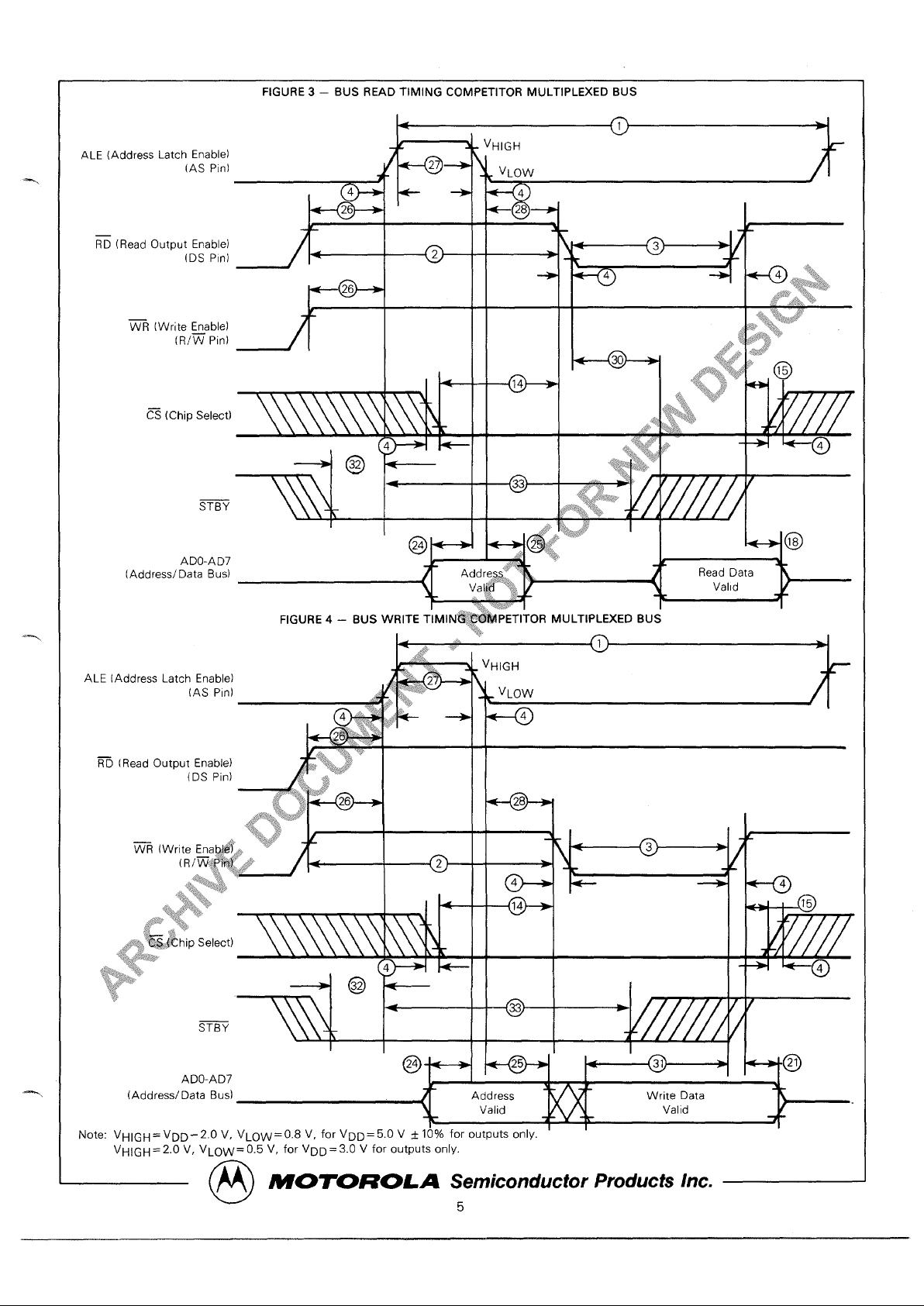
FIGURE 3 – BUS READ TIMING COMPETITOR MULTIPLEXED BUS
‘LE(AddressLatch
~ (Read Output Enable)
(DS Pin)
I IL
C= (Chip Select)
STBY
ADO-AD7
(Address/ Data Bus)
FIGURE 4 – BUS WRITE TIMINti?@PETITOR MULTIPLEXED BUS
@- *W
25 . 31
< ;
‘-
J
A
@
ADO-AD7
(Address/ Data
Bus) Address Write Data
Valid Valld
Note: VHIGH=VDD-2.O V, VLOW=O.8 V, for VDD=5.O V A 10% for outputs only.
VHIGH=2.O V, VLOW=O.5 V, for VDD=3.O V for outputs only.
@
MOTOROLA Semiconductor Products Inc.
5
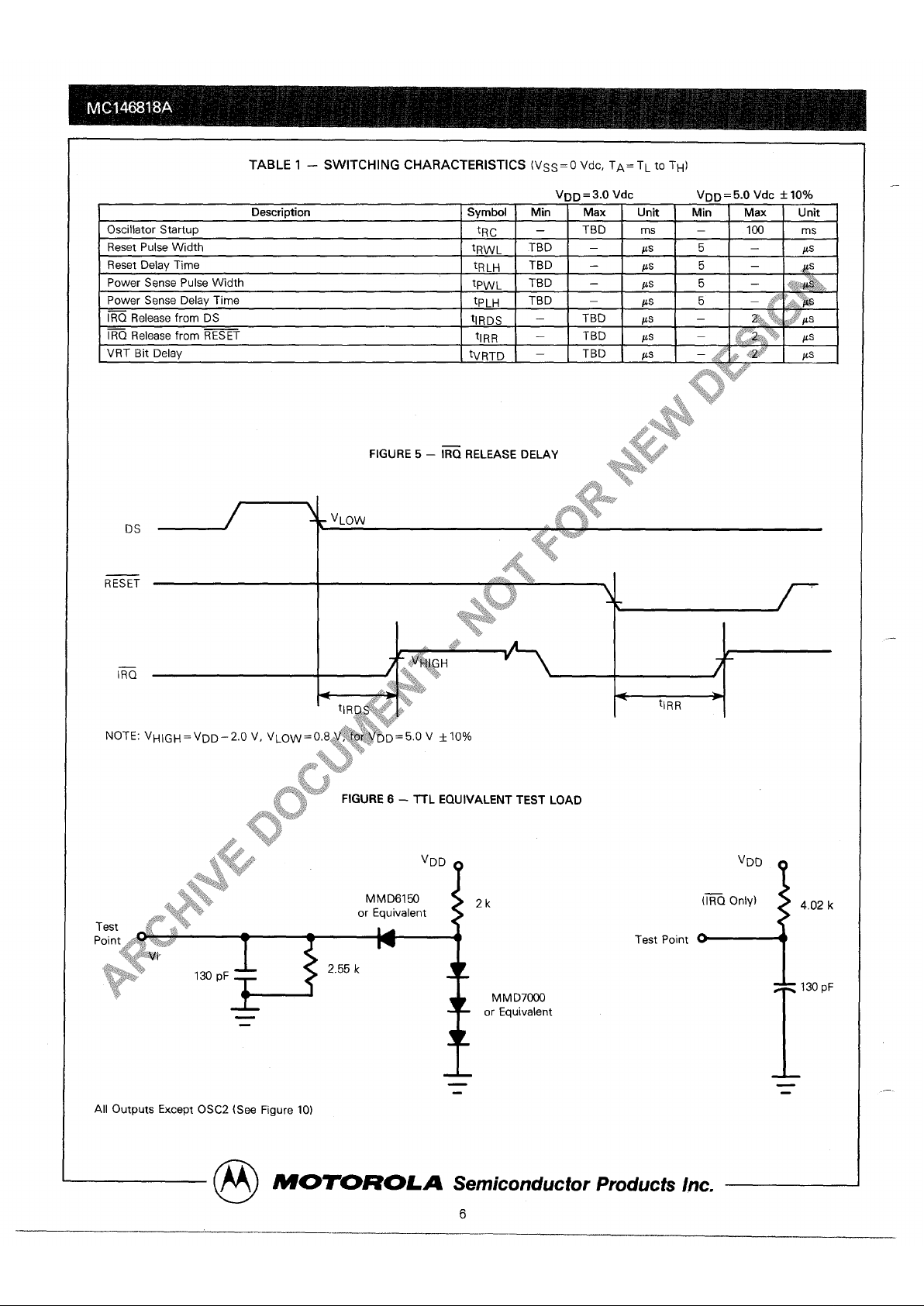
TABLE 1 – SWITCHING CHARACTERISTICS (VSS=O Vdc, TA= TL to TH)
VDD=3.O Vdc
VDD = 5.0 Vdc & 10”A
I
Description I SymbolIMin
I
Max
I
Unit
I
Min
I
Max
I
Unit
I Oscillator Startu~
ltRrl– lTBDlms]– ll~lmsl
1
Reset Pulse Width
I
tRWL[TBD
I
—
I
KS
I
51–
I
ps
I
Reset Delay Time
tRLH
I
TBD I –
I
ps
I
51–
&s
DA,.,-.
C---- D, ,1-- !AI; A+L I +-, .,, TDn I ..- C I I ‘i\!
DS
RESET
ITQ
.
All Outputs Except OSC2 (See Figure 10)
2k
MM D7000
or Equivalent
.
VDD
(KQ OnIV)
T
L 130pF
m
MOTOROLA Semiconductor Products Inc.
6
-.
.—
.—
—
 Loading...