


Semiconductor Components Industries, LLC, 2000
March, 2000 – Rev. 6
1 Publication Order Number:
MC14541B/D
MC14541B
Programmable Timer
The MC14541B programmable timer consists of a 16–stage binary
counter, an integrated oscillator for use with an external capacitor and
two resistors, an automatic power–on reset circuit, and output control
logic.
Timing is initialized by turning on power , whereupon the power–on
reset is enabled and initializes the counter, within the specified V
DD
range. With the power already on, an external reset pulse can be
applied. Upon release of the initial reset command, the oscillator will
oscillate with a frequency determined by the external RC network. The
16–stage counter divides the oscillator frequency (f
osc
) with the n
th
stage frequency being f
osc
/2n.
• A vailable Outputs 2
8
, 210, 213 or 2
16
• Increments on Positive Edge Clock Transitions
• Built–in Low Power RC Oscillator (± 2% accuracy over temperature
range and ± 20% supply and ± 3% over processing at < 10 kHz)
• Oscillator May Be Bypassed if External Clock Is A vailable (Apply
external clock to Pin 3)
• External Master Reset Totally Independent of Automatic Reset
Operation
• Operates as 2
n
Frequency Divider or Single Transition Timer
• Q/Q Select Provides Output Logic Level Flexibility
• Reset (auto or master) Disables Oscillator During Resetting to
Provide No Active Power Dissipation
• Clock Conditioning Circuit Permits Operation with Very Slow Clock
Rise and Fall Times
• Automatic Reset Initializes All Counters On Power Up
• Supply Voltage Range = 3.0 Vdc to 18 Vdc with Auto Reset
Supply Voltage Range = Disabled (Pin 5 = V
DD
)
Supply Voltage Range = 8.5 Vdc to 18 Vdc with Auto Reset
Supply Voltage Range = Enabled (Pin 5 = VSS)
MAXIMUM RATINGS (Voltages Referenced to V
SS
) (Note 2.)
Symbol
Parameter Value Unit
V
DD
DC Supply Voltage Range –0.5 to +18.0 V
Vin, V
out
Input or Output Voltage Range
(DC or Transient)
–0.5 to VDD + 0.5 V
I
in
Input Current (DC or Transient) ±10 (per Pin) mA
I
out
Output Current (DC or Transient) ±45 (per Pin) mA
P
D
Power Dissipation,
per Package (Note 3.)
500 mW
T
A
Ambient Temperature Range –55 to +125 °C
T
stg
Storage Temperature Range –65 to +150 °C
T
L
Lead Temperature
(8–Second Soldering)
260 °C
2. Maximum Ratings are those values beyond which damage to the device
may occur.
3. Temperature Derating:
Plastic “P and D/DW” Packages: – 7.0 mW/_C From 65_C T o 125_C
http://onsemi.com
A = Assembly Location
WL or L = Wafer Lot
YY or Y = Year
WW or W = Work Week
Device Package Shipping
ORDERING INFORMATION
MC14541BCP PDIP–14 2000/Box
MC14541BD SOIC–14 55/Rail
MC14541BDR2 SOIC–14 2500/Tape & Reel
1. For ordering information on the EIAJ version of
the SOIC packages, please contact your local
ON Semiconductor representative.
MC14541BDTR2 TSSOP–14 2500/Tape & Reel
MC14541BDT TSSOP–14 96/Rail
MC14541BF SOEIAJ–14 See Note 1.
This device contains protection circuitry to guard
against damage due to high static voltages or electric
fields. However, precautions must be taken to avoid applications of any voltage higher than maximum rated
voltages to this high–impedance circuit. For proper
operation, V
in
and V
out
should be constrained to the
range V
SS
v (Vin or V
out
) v VDD.
Unused inputs must always be tied to an appropriate
logic voltage level (e.g., either V
SS
or VDD). Unused out-
puts must be left open.
MC14541BFEL SOEIAJ–14 See Note 1.
MARKING
DIAGRAMS
1
14
PDIP–14
P SUFFIX
CASE 646
MC14541BCP
AWLYYWW
SOIC–14
D SUFFIX
CASE 751A
TSSOP–14
DT SUFFIX
CASE 948G
1
14
14541B
AWLYWW
14
541B
ALYW
1
14
SOEIAJ–14
F SUFFIX
CASE 965
1
14
MC14541B
AWLYWW
MC14541B
http://onsemi.com
2
PIN ASSIGNMENT
NC = NO CONNECTION
11
12
13
14
8
9
105
4
3
2
1
7
6
MODE
NC
A
B
V
DD
Q
Q/Q
SEL
NC
R
S
C
tc
R
tc
V
SS
MR
AR
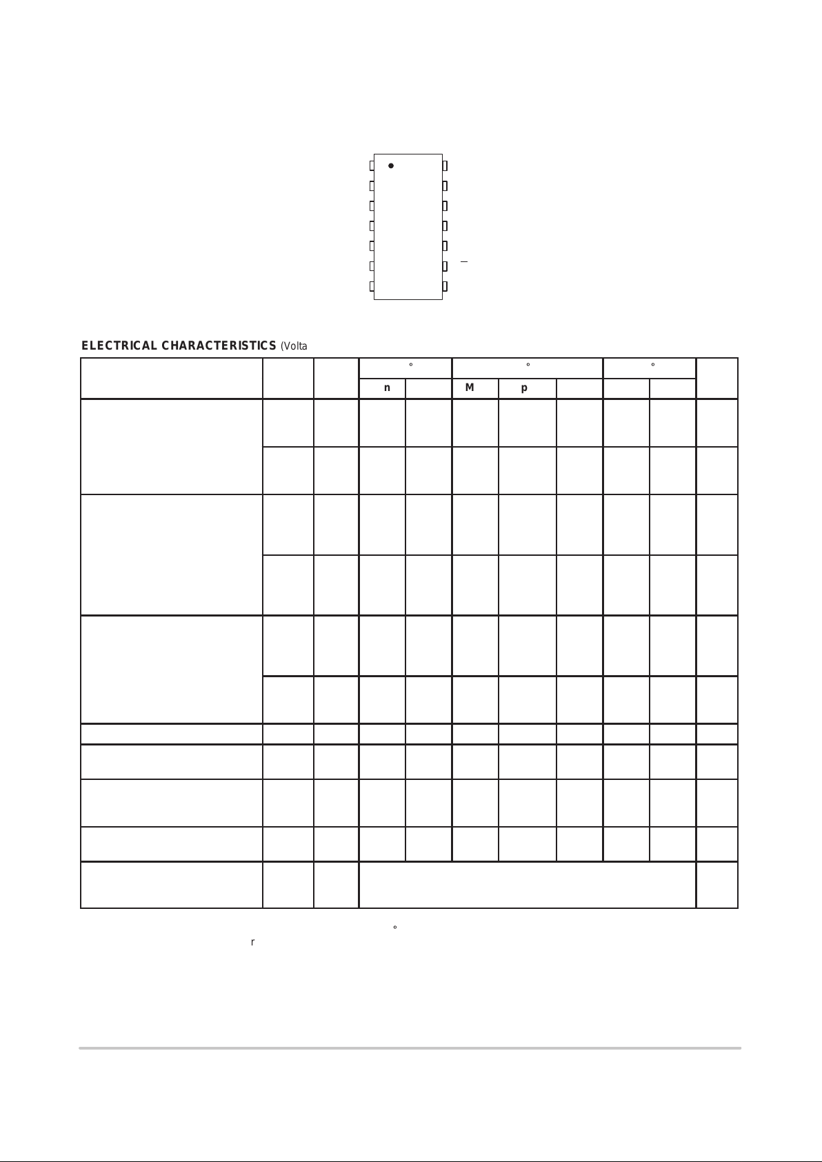
ELECTRICAL CHARACTERISTICS (Voltages Referenced to V
SS
)
V
DD
– 55_C 25_C 125_C
Characteristic Symbol
Vdc
Min Max Min Typ
(4.)
Max Min Max
Unit
Output Voltage “0” Level
V
in
= VDD or 0
V
OL
5.0
10
15
—
—
—
0.05
0.05
0.05
—
—
—
0
0
0
0.05
0.05
0.05
—
—
—
0.05
0.05
0.05
Vdc
“1” Level
V
in
= 0 or V
DD
V
OH
5.0
10
15
4.95
9.95
14.95
—
—
—
4.95
9.95
14.95
5.0
10
15
—
—
—
4.95
9.95
14.95
—
—
—
Vdc
Input Voltage “0” Level
(V
O
= 4.5 or 0.5 Vdc)
(V
O
= 9.0 or 1.0 Vdc)
(V
O
= 13.5 or 1.5 Vdc)
V
IL
5.0
10
15
—
—
—
1.5
3.0
4.0
—
—
—
2.25
4.50
6.75
1.5
3.0
4.0
—
—
—
1.5
3.0
4.0
Vdc
“1” Level
(V
O
= 0.5 or 4.5 Vdc)
(V
O
= 1.0 or 9.0 Vdc)
(V
O
= 1.5 or 13.5 Vdc)
V
IH
5.0
10
15
3.5
7.0
11
—
—
—
3.5
7.0
11
2.75
5.50
8.25
—
—
—
3.5
7.0
11
—
—
—
Vdc
Output Drive Current
(V
OH
= 2.5 Vdc) Source
(V
OH
= 9.5 Vdc)
(V
OH
= 13.5 Vdc)
I
OH
5.0
10
15
– 7.96
– 4.19
– 16.3
—
—
—
– 6.42
– 3.38
– 13.2
– 12.83
– 6.75
– 26.33
—
—
—
– 4.49
– 2.37
– 9.24
—
—
—
mAdc
(VOL = 0.4 Vdc) Sink
(V
OL
= 0.5 Vdc)
(V
OL
= 1.5 Vdc)
I
OL
5.0
10
15
1.93
4.96
19.3
—
—
—
1.56
4.0
15.6
3.12
8.0
31.2
—
—
—
1.09
2.8
10.9
—
—
—
mAdc
Input Current I
in
15 — ± 0.1 — ±0.00001 ± 0.1 — ± 1.0 µAdc
Input Capacitance
(V
in
= 0)
C
in
— — — — 5.0 7.5 — — pF
Quiescent Current
(Pin 5 is High)
Auto Reset Disabled
I
DD
5.0
10
15
—
—
—
5.0
10
20
—
—
—
0.005
0.010
0.015
5.0
10
20
—
—
—
150
300
600
µAdc
Auto Reset Quiescent Current
(Pin 5 is low)
I
DDR
10
15
—
—
250
500
—
—
30
82
250
500
—
—
1500
2000
µAdc
Supply Current
(5.) (6.)
(Dynamic plus Quiescent)
I
D
5.0
10
15
ID = (0.4 µA/kHz) f + I
DD
ID = (0.8 µA/kHz) f + I
DD
ID = (1.2 µA/kHz) f + I
DD
µAdc
4. Data labelled “Typ” is not to be used for design purposes but is intended as an indication of the IC’s potential performance.
5. The formulas given are for the typical characteristics only at 25_C.
6. When using the on chip oscillator the total supply current (in µAdc) becomes: IT = ID + 2 Ctc VDD f x 10–3 where ID is in µA, Ctc is in pF,
V
DD
in Volts DC, and f in kHz. (see Fig. 3) Dissipation during power–on with automatic reset enabled is typically 50 µA @ VDD = 10 Vdc.

MC14541B
http://onsemi.com
3
SWITCHING CHARACTERISTICS
(7.)
(C
L
= 50 pF, T
A
= 25_C)
Characteristic
Symbol V
DD
Min Typ
(8.)
Max Unit
Output Rise and Fall Time
t
TLH
, t
THL
= (1.5 ns/pF) CL + 25 ns
t
TLH
, t
THL
= (0.75 ns/pF) CL + 12.5 ns
t
TLH
, t
THL
= (0.55 ns/pF) CL + 9.5 ns
t
TLH
,
t
THL
5.0
10
15
—
—
—
100
50
40
200
100
80
ns
Propagation Delay, Clock to Q (28 Output)
t
PLH
, t
PHL
= (1.7 ns/pF) CL + 3415 ns
t
PLH
, t
PHL
= (0.66 ns/pF) CL + 1217 ns
t
PLH
, t
PHL
= (0.5 ns/pF) CL + 875 ns
t
PLH
t
PHL
5.0
10
15
—
—
—
3.5
1.25
0.9
10.5
3.8
2.9
µs
Propagation Delay, Clock to Q (216 Output)
t
PHL
, t
PLH
= (1.7 ns/pF) CL + 5915 ns
t
PHL
, t
PLH
= (0.66 ns/pF) CL + 3467 ns
t
PHL
, t
PLH
= (0.5 ns/pF) CL + 2475 ns
t
PHL
t
PLH
5.0
10
15
—
—
—
6.0
3.5
2.5
18
10
7.5
µs
Clock Pulse Width t
WH(cl)
5.0
10
15
900
300
225
300
100
85
—
—
—
ns
Clock Pulse Frequency (50% Duty Cycle) f
cl
5.0
10
15
—
—
—
1.5
4.0
6.0
0.75
2.0
3.0
MHz
MR Pulse Width t
WH(R)
5.0
10
15
900
300
225
300
100
85
—
—
—
ns
Master Reset Removal Time t
rem
5.0
10
15
420
200
200
210
100
100
—
—
—
ns
7. The formulas given are for the typical characteristics only at 25_C.
8. Data labelled “Typ” is not to be used for design purposes but is intended as an indication of the IC’s potential performance.
Figure 1. Power Dissipation Test Circuit
and Waveform
Figure 2. Switching Time Test Circuit
and Waveforms
PULSE
GENERATOR
V
DD
C
L
Q
R
S
AR
Q/Q
SELECT
MODE
A
B
MR
V
SS
20 ns 20 ns
90%
50%
10%
50%
DUTY CYCLE
(Rtc AND Ctc OUTPUTS ARE LEFT OPEN)
PULSE
GENERATOR
V
DD
R
S
AR
Q/Q
SELECT
MODE
A
B
MR
V
SS
C
L
Q
20 ns
90%
50%
20 ns
10%
R
S
Q
t
PLH
50%
90%
50%
10%
50%
t
TLH
t
THL
t
PHL

MC14541B
http://onsemi.com
4
EXPANDED BLOCK DIAGRAM
A12
B13
R
tc
1
C
tc
2
R
S
3
5
AUTO RESET
OSC
RESET
C
2
8
8–STAGE
COUNTER
RESET
POWER–ON
RESET
6
MASTER RESET
2
10213216
C
8–STAGE
COUNTER
RESET
1 OF 4
MUX
10
MODE
9
Q/Q
SELECT
8Q
V
DD
= PIN 14
V
SS
= PIN 7
FREQUENCY SELECTION TABLE
A B
Number of
Counter Stages
n
Count
2
n
0 0 13 8192
0 1 10 1024
1 0 8 256
1 1 16 65536
TRUTH TABLE
State
Pin
0 1
Auto Reset, 5 Auto Reset
Operating
Auto Reset Disabled
Master Reset, 6 Timer Operational Master Reset On
Q/Q,9Output Initially Low
After Reset
Output Initially High
After Reset
Mode, 10 Single Cycle Mode Recycle Mode
Figure 3. Oscillator Circuit Using RC Configuration
3
R
S
R
TC
C
tc
21
TO CLOCK
CIRCUIT
INTERNAL
RESET

MC14541B
http://onsemi.com
5
TYPICAL RC OSCILLATOR CHARACTERISTICS
Figure 4. RC Oscillator Stability
Figure 5. RC Oscillator Frequency as a
Function of R
tc
and C
tc
8.0
4.0
0
–4.0
–8.0
–12
–16
1251007550250–25–55
T
A
, AMBIENT TEMPERATURE (°C)
F
R
E
QU
E
NC
Y
D
E
V
I
A
TIO
N
(%
)
VDD = 15 V
10 V
5.0 V
RS = 0, f = 10.15 kHz @ VDD = 10 V, TA = 25°C
RS = 120 kΩ, f = 7.8 kHz @ VDD = 10 V, TA = 25°C
R
TC
= 56 kΩ,
C = 1000 pF
100
0.1
0.2
0.5
1.0
2.0
5.0
10
20
50
1.0 k 10 k 100 k 1.0 m
f, OSCILLATOR FREQUENCY (kHz)
RTC, RESISTANCE (OHMS)
0.0001 0.001 0.01 0.1
C, CAPACITANCE (µF)
VDD = 10 V
f AS A FUNCTION
OF R
TC
(C = 1000 pF)
(R
S
≈ 2RTC)
f AS A FUNCTION
OF C
(R
TC
= 56 kΩ)
(R
S
= 120 kΩ)
OPERA TING CHARACTERISTICS
With Auto Reset pin set to a “0” the counter circuit is
initialized by turning on power. Or with power already on,
the counter circuit is reset when the Master Reset pin is set
to a “1”. Both types of reset will result in synchronously
resetting all counter stages independent of counter state.
Auto Reset pin when set to a “1” provides a low power
operation.
The RC oscillator as shown in Figure 3 will oscillate with
a frequency determined by the external RC network i.e.,
if (1 kHz v f v 100 kHz)
2.3 R
tcCtc
1
f =
and RS ≈ 2 R
tc
where RS ≥ 10 kΩ
The time select inputs (A and B) provide a two–bit address
to output any one of four counter stages (28, 210, 213 and
216). The 2n counts as shown in the Frequency Selection
Table represents the Q output of the Nth stage of the counter.
When A is “1”, 216 is selected for both states of B. However,
when B is “0”, normal counting is interrupted and the 9th
counter stage receives its clock directly from the oscillator
(i.e., effectively outputting 2
8
).
The Q/Q select output control pin provides for a choice of
output level. When the counter is in a reset condition and
Q/Q select pin is set to a “0” the Q output is a “0”,
correspondingly when Q/Q select pin is set to a “1” the Q
output is a “1”.
When the mode control pin is set to a “1”, the selected
count is continually transmitted to the output. But, with
mode pin “0” and after a reset condition the R
S
flip–flop (see
Expanded Block Diagram) resets, counting commences,
and after 2
n–1
counts the RS flip–flop sets which causes the
output to change state. Hence, after another 2
n–1
counts the
output will not change. Thus, a Master Reset pulse must be
applied or a change in the mode pin level is required to reset
the single cycle operation.
DIGIT AL TIMER APPLICATION
R
tc
C
tc
NC
R
S
AR
MR
INPUT
t
MR
V
DD
B
A
N.C.
OUTPUT
V
DD
MODE
Q/Q
t + t
MR
1
2
3
4
5
6
78
9
10
11
12
13
14
When Master Reset (MR) receives a positive pulse, the
internal counters and latch are reset. The Q output goes high
and remains high until the selected (via A and B) number of
clock pulses are counted, the Q output then goes low and
remains low until another input pulse is received.
This “one shot” is fully retriggerable and as accurate as the
input frequency. An external clock can be used (pin 3 is the
clock input, pins 1 and 2 are outputs) if additional accuracy
is needed.
Notice that a setup time equal to the desired pulse width
output is required immediately following initial power up,
during which time Q output will be high.

MC14541B
http://onsemi.com
6
P ACKAGE DIMENSIONS
P SUFFIX
PLASTIC DIP PACKAGE
CASE 646–06
ISSUE M
17
14 8
B
A
DIM MIN MAX MIN MAX
MILLIMETERSINCHES
A 0.715 0.770 18.16 18.80
B 0.240 0.260 6.10 6.60
C 0.145 0.185 3.69 4.69
D 0.015 0.021 0.38 0.53
F 0.040 0.070 1.02 1.78
G 0.100 BSC 2.54 BSC
H 0.052 0.095 1.32 2.41
J 0.008 0.015 0.20 0.38
K 0.115 0.135 2.92 3.43
L
M ––– 10 ––– 10
N 0.015 0.039 0.38 1.01
__
NOTES:
1. DIMENSIONING AND TOLERANCING PER ANSI
Y14.5M, 1982.
2. CONTROLLING DIMENSION: INCH.
3. DIMENSION L TO CENTER OF LEADS WHEN
FORMED PARALLEL.
4. DIMENSION B DOES NOT INCLUDE MOLD FLASH.
5. ROUNDED CORNERS OPTIONAL.
F
HG
D
K
C
SEATING
PLANE
N
–T–
14 PL
M
0.13 (0.005)
L
M
J
0.290 0.310 7.37 7.87
D SUFFIX
PLASTIC SOIC PACKAGE
CASE 751A–03
ISSUE F
NOTES:
1. DIMENSIONING AND TOLERANCING PER ANSI
Y14.5M, 1982.
2. CONTROLLING DIMENSION: MILLIMETER.
3. DIMENSIONS A AND B DO NOT INCLUDE
MOLD PROTRUSION.
4. MAXIMUM MOLD PROTRUSION 0.15 (0.006)
PER SIDE.
5. DIMENSION D DOES NOT INCLUDE DAMBAR
PROTRUSION. ALLOWABLE DAMBAR
PROTRUSION SHALL BE 0.127 (0.005) TOTAL
IN EXCESS OF THE D DIMENSION AT
MAXIMUM MATERIAL CONDITION.
–A–
–B–
G
P
7 PL
14 8
71
M
0.25 (0.010) B
M
S
B
M
0.25 (0.010) A
S
T
–T–
F
R X 45
SEATING
PLANE
D 14 PL
K
C
J
M
_
DIM MIN MAX MIN MAX
INCHESMILLIMETERS
A 8.55 8.75 0.337 0.344
B 3.80 4.00 0.150 0.157
C 1.35 1.75 0.054 0.068
D 0.35 0.49 0.014 0.019
F 0.40 1.25 0.016 0.049
G 1.27 BSC 0.050 BSC
J 0.19 0.25 0.008 0.009
K 0.10 0.25 0.004 0.009
M 0 7 0 7
P 5.80 6.20 0.228 0.244
R 0.25 0.50 0.010 0.019
____

MC14541B
http://onsemi.com
7
P ACKAGE DIMENSIONS
DT SUFFIX
PLASTIC TSSOP PACKAGE
CASE 948G–01
ISSUE O
DIM MIN MAX MIN MAX
INCHESMILLIMETERS
A 4.90 5.10 0.193 0.200
B 4.30 4.50 0.169 0.177
C ––– 1.20 ––– 0.047
D 0.05 0.15 0.002 0.006
F 0.50 0.75 0.020 0.030
G 0.65 BSC 0.026 BSC
H 0.50 0.60 0.020 0.024
J 0.09 0.20 0.004 0.008
J1 0.09 0.16 0.004 0.006
K 0.19 0.30 0.007 0.012
K1 0.19 0.25 0.007 0.010
L 6.40 BSC 0.252 BSC
M 0 8 0 8
NOTES:
1. DIMENSIONING AND TOLERANCING PER ANSI
Y14.5M, 1982.
2. CONTROLLING DIMENSION: MILLIMETER.
3. DIMENSION A DOES NOT INCLUDE MOLD
FLASH, PROTRUSIONS OR GATE BURRS. MOLD
FLASH OR GATE BURRS SHALL NOT EXCEED
0.15 (0.006) PER SIDE.
4. DIMENSION B DOES NOT INCLUDE
INTERLEAD FLASH OR PROTRUSION.
INTERLEAD FLASH OR PROTRUSION SHALL NOT
EXCEED
0.25 (0.010) PER SIDE.
5. DIMENSION K DOES NOT INCLUDE DAMBAR
PROTRUSION. ALLOWABLE DAMBAR
PROTRUSION SHALL BE 0.08 (0.003) TOTAL IN
EXCESS OF THE K DIMENSION AT MAXIMUM
MATERIAL CONDITION.
6. TERMINAL NUMBERS ARE SHOWN FOR
REFERENCE ONLY.
7. DIMENSION A AND B ARE TO BE
DETERMINED AT DATUM PLANE –W–.
____
S
U0.15 (0.006) T
2X L/2
S
U
M
0.10 (0.004) V
S
T
L
–U–
SEATING
PLANE
0.10 (0.004)
–T–
SECTION N–N
DETAIL E
J
J1
K
K1
DETAIL E
F
M
–W–
0.25 (0.010)
8
14
7
1
PIN 1
IDENT.
H
G
A
D
C
B
S
U0.15 (0.006) T
–V–
14X REFK
N
N

MC14541B
http://onsemi.com
8
P ACKAGE DIMENSIONS
F SUFFIX
PLASTIC EIAJ SOIC PACKAGE
CASE 965–01
ISSUE O
H
E
A
1
DIM MIN MAX MIN MAX
INCHES
––– 2.05 ––– 0.081
MILLIMETERS
0.05 0.20 0.002 0.008
0.35 0.50 0.014 0.020
0.18 0.27 0.007 0.011
9.90 10.50 0.390 0.413
5.10 5.45 0.201 0.215
1.27 BSC 0.050 BSC
7.40 8.20 0.291 0.323
0.50 0.85 0.020 0.033
1.10 1.50 0.043 0.059
0
0.70 0.90 0.028 0.035
––– 1.42 ––– 0.056
A
1
H
E
Q
1
L
E
_
10
_
0
_
10
_
L
E
Q
1
_
NOTES:
1. DIMENSIONING AND TOLERANCING PER ANSI
Y14.5M, 1982.
2. CONTROLLING DIMENSION: MILLIMETER.
3. DIMENSIONS D AND E DO NOT INCLUDE
MOLD FLASH OR PROTRUSIONS AND ARE
MEASURED AT THE PARTING LINE. MOLD FLASH
OR PROTRUSIONS SHALL NOT EXCEED 0.15
(0.006) PER SIDE.
4. TERMINAL NUMBERS ARE SHOWN FOR
REFERENCE ONLY.
5. THE LEAD WIDTH DIMENSION (b) DOES NOT
INCLUDE DAMBAR PROTRUSION. ALLOWABLE
DAMBAR PROTRUSION SHALL BE 0.08 (0.003)
TOTAL IN EXCESS OF THE LEAD WIDTH
DIMENSION AT MAXIMUM MATERIAL CONDITION.
DAMBAR CANNOT BE LOCATED ON THE LOWER
RADIUS OR THE FOOT. MINIMUM SPACE
BETWEEN PROTRUSIONS AND ADJACENT LEAD
TO BE 0.46 ( 0.018).
0.13 (0.005)
M
0.10 (0.004)
D
Z
E
1
14 8
7
e
A
b
VIEW P
c
L
DETAIL P
M
A
b
c
D
E
e
0.50
M
Z
ON Semiconductor and are trademarks of Semiconductor Components Industries, LLC (SCILLC). SCILLC reserves the right to make changes
without further notice to any products herein. SCILLC makes no warranty , representation or guarantee regarding the suitability of its products for any particular
purpose, nor does SCILLC assume any liability arising out of the application or use of any product or circuit, and specifically disclaims any and all liability ,
including without limitation special, consequential or incidental damages. “Typical” parameters which may be provided in SCILLC data sheets and/or
specifications can and do vary in different applications and actual performance may vary over time. All operating parameters, including “Typicals” must be
validated for each customer application by customer’s technical experts. SCILLC does not convey any license under its patent rights nor the rights of others.
SCILLC products are not designed, intended, or authorized for use as components in systems intended for surgical implant into the body, or other applications
intended to support or sustain life, or for any other application in which the failure of the SCILLC product could create a situation where personal injury or
death may occur. Should Buyer purchase or use SCILLC products for any such unintended or unauthorized application, Buyer shall indemnify and hold
SCILLC and its officers, employees, subsidiaries, affiliates, and distributors harmless against all claims, costs, damages, and expenses, and reasonable
attorney fees arising out of, directly or indirectly , any claim of personal injury or death associated with such unintended or unauthorized use, even if such claim
alleges that SCILLC was negligent regarding the design or manufacture of the part. SCILLC is an Equal Opportunity/Affirmative Action Employer .
PUBLICATION ORDERING INFORMATION
CENTRAL/SOUTH AMERICA:
Spanish Phone: 303–308–7143 (Mon–Fri 8:00am to 5:00pm MST)
Email: ONlit–spanish@hibbertco.com
ASIA/PACIFIC : LDC for ON Semiconductor – Asia Support
Phone: 303–675–2121 (Tue–Fri 9:00am to 1:00pm, Hong Kong Time)
T oll Free from Hong Kong & Singapore:
001–800–4422–3781
Email: ONlit–asia@hibbertco.com
JAPAN: ON Semiconductor, Japan Customer Focus Center
4–32–1 Nishi–Gotanda, Shinagawa–ku, T okyo, Japan 141–8549
Phone: 81–3–5740–2745
Email: r14525@onsemi.com
ON Semiconductor Website: http://onsemi.com
For additional information, please contact your local
Sales Representative.
MC14541B/D
NORTH AMERICA Literature Fulfillment:
Literature Distribution Center for ON Semiconductor
P.O. Box 5163, Denver, Colorado 80217 USA
Phone: 303–675–2175 or 800–344–3860 T oll Free USA/Canada
Fax: 303–675–2176 or 800–344–3867 Toll Free USA/Canada
Email: ONlit@hibbertco.com
Fax Response Line: 303–675–2167 or 800–344–3810 T oll Free USA/Canada
N. American Technical Support: 800–282–9855 Toll Free USA/Canada
EUROPE: LDC for ON Semiconductor – European Support
German Phone: (+1) 303–308–7140 (M–F 1:00pm to 5:00pm Munich Time)
Email: ONlit–german@hibbertco.com
French Phone: (+1) 303–308–7141 (M–F 1:00pm to 5:00pm Toulouse T ime)
Email: ONlit–french@hibbertco.com
English Phone: (+1) 303–308–7142 (M–F 12:00pm to 5:00pm UK Time)
Email: ONlit@hibbertco.com
EUROPEAN TOLL–FREE ACCESS*: 00–800–4422–3781
*Available from Germany, France, Italy , England, Ireland
 Loading...