MC145220MOTOROLA
1
" !
!"
BiCMOS
The MC145220 is a low–voltage, single–chip frequency synthesizer with
serial interface capable of direct usage up to 1.1 GHz. The device simultaneously supports two loops. The two on–chip dual–modulus prescalers may be
independently programmed to divide by either 32/33 or 64/65.
The device consists of two dual–modulus prescalers, two 6–stage A
counters, two 12–stage N counters, two fully programmable 13–stage R
(reference) counters, and two lock detectors. Four phase/frequency detectors
are included: two with current source/sink outputs and two with double–ended
outputs.
The counters are programmed via a synchronous serial port which is SPI
compatible. The serial port is byte–oriented to facilitate control via an MCU. Due
to the innovative BitGrabber Plus registers, the MC145220 may be cascaded
with other peripherals featuring BitGrabber Plus without requiring leading
dummy bits or multiple address bits in the serial data stream. In addition,
BitGrabber Plus peripherals may be cascaded with existing BitGrabber
peripherals. Because this device is a dual synthesizer, a single steering bit is
used in the serial data stream to direct the data to either side of the chip.
The phase/frequency detectors have linear transfer functions (no dead
zones). The current delivered by the current source/sink outputs is controllable
via the serial port.
Also featured are low–power standby for either one or both loops and
on–board support of an external crystal. In addition, the part may be configured
such that the REFin pin accepts an external reference signal. In this
configuration, the REF
out
pin may be programmed to output the REF
in
frequency divided by 1, 2, 4, 8, or 16.
• Operating Frequency: 40 to 1100 MHz
• Operating Supply Voltage Range: 2.7 to 5.5 V
• Supply Current: Both PLLs Operating — 12 mA Nominal
One PLL Operating, One on Standby — 6.5 mA Nominal
Both PLLs on Standby — 30 µA Maximum
• Phase Detector Output Current: Up to 2 mA @ 5 V
Up to 1 mA @ 3 V
• Operating Temperature Range: – 40 to 85°C
• Independent R Counters Allow Use of Different Step Sizes for Each Loop
• Double–Buffered R Register — Reference and Loop Divide Ratios
Updated Simultaneously
• R Counter Division Range: 1 and 10 to 8,191
• Dual–Modulus Capability Provides Total Division of the VCO Frequency up
to 262,143
• Direct Interface to Motorola SPI Data Port
• Evaluation Kit Available (Part Number MC145220EVK)
• See Application Note AN1253/D for Low–Pass Filter Design, and
AN1277/D for Offset Reference PLLs for Fine Resolution or Fast Hopping
NOTE: This product has been evaluated for operation over a wider range than 40 MHz to 1.1 GHz. If your design requires a wider
frequency range, contact your local Motorola representative for further information.
BitGrabber and BitGrabber Plus are trademarks of Motorola, Inc.
Order this document
by MC145220/D
SEMICONDUCTOR TECHNICAL DATA
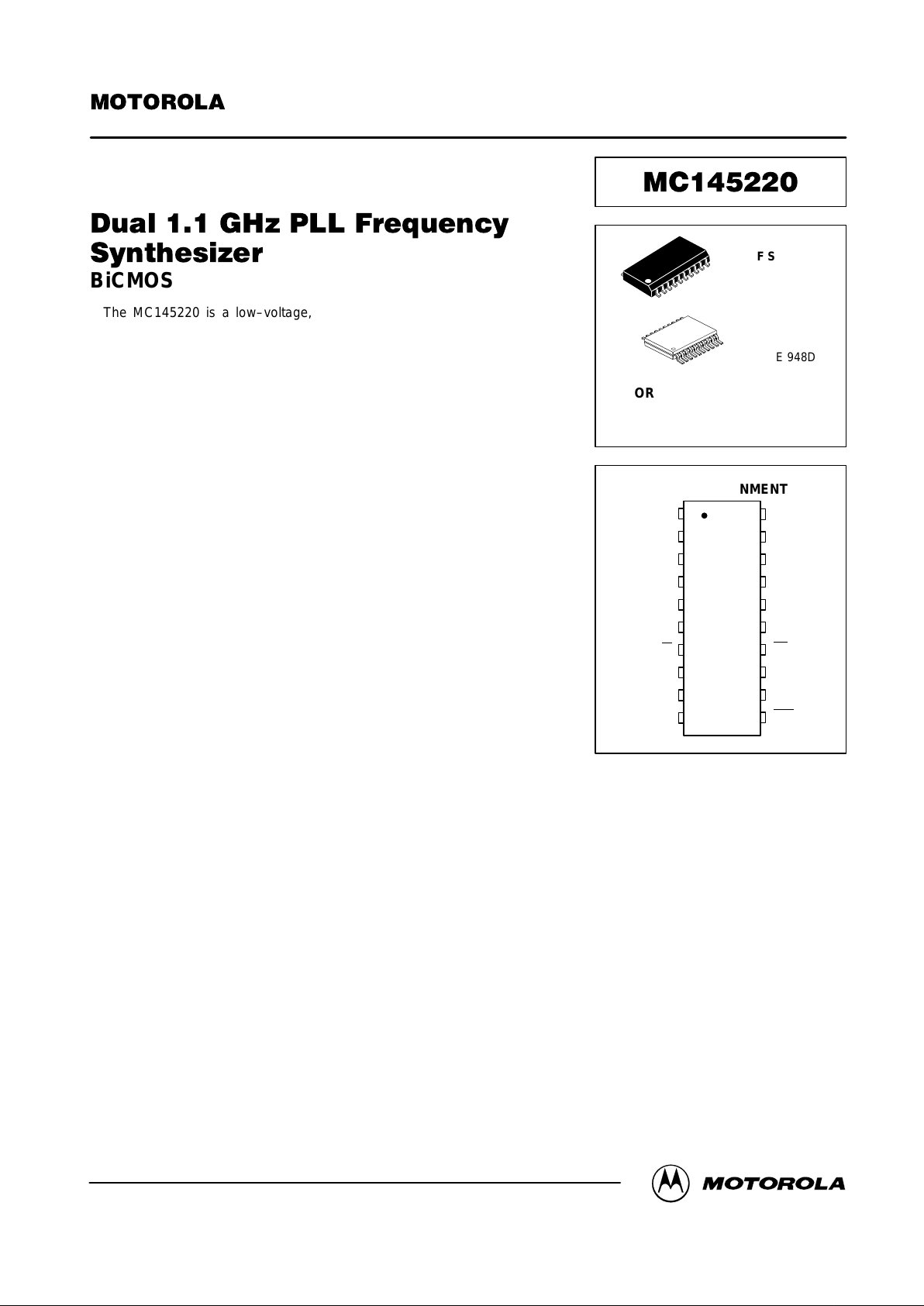
PIN ASSIGNMENT
F SUFFIX
SOG PACKAGE
CASE 803C
DT SUFFIX
TSSOP
CASE 948D
ORDERING INFORMATION
MC145220F SOG Package
MC145220DT TSSOP
20
1
20
1
GND
′
LD
′
13
14
15
16
CLK
D
in
PD
out
′/φR′
8
7
6
5
4
3
2
1
f
in
f
in
GND
PD
out
/
φ
R
LD
REF
out
REF
in
18
19
20
17
fin′
ENB11
12
10
9
OUTPUT A
V+
V+
′
Rx/
φ
V
Rx′/
φV′
fin′
Motorola, Inc. 1998
REV 4
1/98 TN98012300
MC145220 MOTOROLA
2
8
7
f
in
f
in
2
1
3
BUFFER
AND
CONTROL
REF
out
REF
in
23
7
13
BitGrabber Plus
R REGISTER
16 BITS
Rs
Rs
′
13–STAGE
R COUNTER
13–STAGE
R
′
COUNTER
BitGrabber Plus
A REGISTER
23 BITS
A AND N COUNTERS
32/33 OR
64/65
PRESCALER
RATIO
18
32/33 OR
64/65
PRESCALER
A
′
& N′ COUNTERS
23
BitGrabber Plus
A
′
REGISTER
23 BITS
RATIO
13
14
f
in
′
fin′
23
24 1/2 STAGE
SHIFT REGISTER
ADDRESS
LOGIC AND
STORAGE
11
20
ENB
D
in
19
CLK
2
5
PLL / PLL
′
SELECT FROM
A REGISTER
(INTERNAL)
MUX
f
R
f
R
′
f
V
f
V
′
PORT
17
16
10
18
PHASE/
FREQUENCY
DETECTOR
PAIR
2
BitGrabber Plus
C
′
REGISTER
7 BITS
LD
′
Rx′/
φV′
OUTPUT A
PD
out
′/φR′
LD
Rx/
φ
V
PD
out
/
φ
R
BitGrabber Plus
C REGISTER
7 BITS
PHASE/
FREQUENCY
DETECTOR
PAIR
STBY
(INTERNAL)
STBY
′
(INTERNAL)
2
4
5
DATA OUT
PIN 9 = V+ (Positive Power to the main PLL, Reference Circuit, and a portion of the Serial Port)
PIN 6 = GND (Ground to the main PLL, Reference Circuit, and a portion of the Serial Port)
PIN 12 = V+′ (Positive Power to PLL′ and a portion of the Serial Port)
PIN 15 = GND′ (Ground to PLL′ and a portion of the Serial Port)
13
18
16
2
3
POLARITY
GAIN
PDA/B SELECT
2
UNUSED
2
TO MUX FOR
OUTPUT A
UNUSED
POLARITY
GAIN
PDA/B SELECT
2
UNUSED
2
2
(INTERNAL)
(INTERNAL)
f
R
′
f
R
f
V
f
V
′
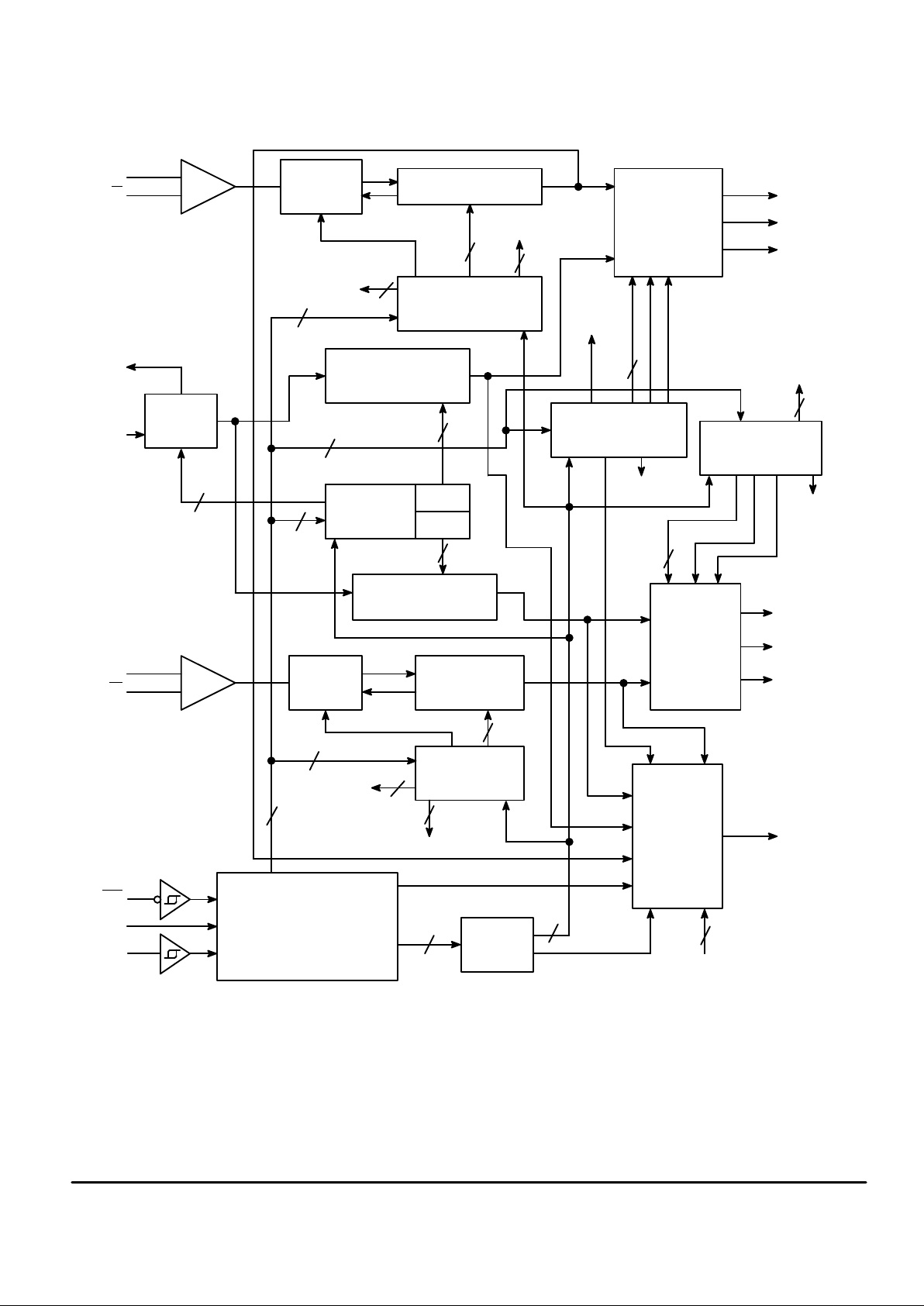
BLOCK DIAGRAM
DOUBLE BUFFER
MC145220MOTOROLA
3
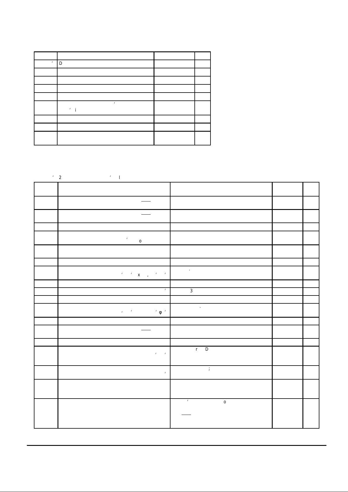
MAXIMUM RATINGS* (Voltages Referenced to GND, unless otherwise stated)
Symbol Parameter Value Unit
V+, V+
i
DC Supply Voltage – 0.5 to + 6.0 V
V
in
DC Input Voltage – 0.5 to V+ + 0.5 V
V
out
DC Output Voltage – 0.5 to V+ + 0.5 V
I
in
DC Input Current, per Pin ± 10 mA
I
out
DC Output Current, per Pin ± 20 mA
I
DC Supply Current, V+, V+i, GND, and
GNDi Pins
30 mA
P
D
Power Dissipation, per Package 300 mW
T
stg
Storage Temperature – 65 to + 150 °C
T
L
Lead Temperature, 1 mm from Case for
10 Seconds
260 °C
*Maximum Ratings are those values beyond which damage to the device may occur.
Functional operation should be restricted to the limits in the Electrical Characteristics
tables or Pin Descriptions section.
ELECTRICAL CHARACTERISTICS
(V+ = V+i = 2.7 to 5.5 V , GND = GNDi, Voltages Referenced to GND, TA = – 40 to 85°C, unless otherwise stated)
Symbol
Parameter Test Condition
Guaranteed
Limit
Unit
V
IL
Maximum Low–Level Input Voltage
(Din, CLK, ENB
, REFin)
Device in Reference Mode, dc Coupled 0.3 x V+ V
V
IH
Minimum High–Level Input Voltage
(Din, CLK, ENB
, REFin)
Device in Reference Mode, dc Coupled 0.7 x V+ V
V
Hys
Minimum Hysteresis Voltage (CLK, ENB) 100 mV
V
OL
Maximum Low–Level Output Voltage
(LD, LDi, REF
out
, Output A)
I
out
= 20 µA, Device in Reference Mode;
Output A Not Selected as Port
0.1 V
V
OH
Minimum High–Level Output Voltage
(REF
out
, Output A)
I
out
= – 20 µA, Device in Reference Mode;
Output A Not Selected as Port
V+ – 0.1 V
I
OL
Minimum Low–Level Output Current (REF
out
) V
out
= 0.3 V 0.5 mA
I
OL
Minimum Low–Level Output Current
(PD
out/φR
, PD
out
i
/φRi
, Rx/φV, Rxi/φVi
)
V
out
= 0.3 V; Phase/Frequency Detectors
Configured with φR, φV Outputs
0.5 mA
I
OL
Minimum Low–Level Output Current (Output A) V
out
= 0.3 V 0.5 mA
I
OL
Minimum Low–Level Output Current (LD, LDi)
V
out
= 0.3 V 0.5 mA
I
OH
Minimum High–Level Output Current (REF
out
) V
out
= V+ – 0.3 V – 0.4 mA
I
OH
Minimum High–Level Output Current
(PD
out/φR
, PD
out
i/φR
i
, Rx/φV, Rxi/φVi
)
V
out
= V+ – 0.3 V; Phase/Frequency Detectors
Configured with φR, φV Outputs
– 0.4 mA
I
OH
Minimum High–Level Output Current (Output A) V
out
= V+ – 0.3 V; Output A Not Selected as Port – 0.4 mA
I
in
Maximum Input Leakage Current
(Din, CLK, ENB, REFin)
Vin = V+ or GND; Device in XTAL Mode ± 1.0 µA
I
in
Maximum Input Current (REFin) Vin = V+ or GND; Device in Reference Mode ± 150 µA
I
OZ
Maximum Output Leakage Current
(PD
out/φR
, PD
out
i
/φRi
)
V
out
= V+ or GND; Phase/Frequency Detectors
Configured with PD
out
Output, Output in High–
Impedance State
± 150 nA
I
OZ
Maximum Output Leakage Current
(Output A, LD, LDi)
V
out
= V+ or GND; Output A Selected as Port;
Output in High–Impedance State
± 5 µA
I
STBY
Maximum Standby Supply Current Vin = V+ or GND; Outputs Open; Both PLLs in
Standby Mode, Shut–Down Crystal Mode or
REF
out
–Static–Low Reference Mode
30 µA
I
T
Total Operating Supply Current
fin = fini
= 1.1 GHz; both loops active;
REFin = 13 MHz @ 1 V p–p;
Output A = Inactive; All Outputs = No Connect;
Din, ENB
, CLK = V+ or GND; Phase/Frequency
Detectors Configured with φR, φV Outputs
* mA
*The nominal value is 12 mA. This is not a guaranteed limit.
This device contains protection circuitry to
guard against damage due to high static voltages or electric fields. However, precautions
must be taken to avoid applications of any voltage higher than maximum rated voltages to this
high–impedance circuit.
MC145220 MOTOROLA
4
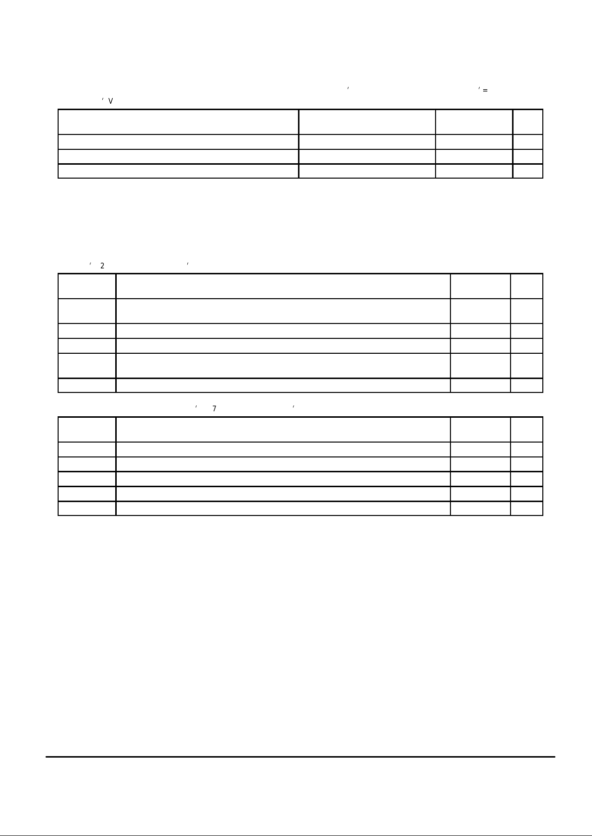
ANALOG CHARACTERISTICS — CURRENT SOURCE/SINK OUTPUTS — PD
out/φR
AND PD
out
′/φR′
(Phase/Frequency Detectors Configured with PD
out
Outputs, I
out
≤ 2 mA @V+ = V+i = 4.5 to 5.5 V , I
out
≤ 1 mA @V+ = V+i = 2.7 to 4.4 V ,
GND = GNDi, Voltages Referenced to GND)
Parameter Test Condition
Guaranteed
Limit
Unit
Maximum Source Current Variation Part–to–Part (Notes 3 and 4) V
out
= 0.5 x V+ ± 20 %
Maximum Sink–versus–Source Mismatch (Note 3) V
out
= 0.5 x V+ 12 %
Output Voltage Range (Note 3) I
out
variation ≤ 20% 0.5 to V+ – 0.5 V V
NOTES:
1. Percentages calculated using the following formula: (Maximum Value – Minimum Value)/Maximum Value.
2. See Rx Pin Description for external resistor values.
3. This parameter is guaranteed for a given temperature within – 40 to 85°C and given supply voltage within 2.7 to 5.5 V.
4. Applicable for the Rx/φV or Rx′/φV′ reference pin tied to the GND or GND′ pin through a resistor. See Pin Descriptions for suggested resistor
values.
AC INTERFACE CHARACTERISTICS
(V+ = V+i = 2.7 to 5.5 V , GND = GNDi, TA = – 40 to 85°C, CL = 25 pF, Input tr = tf = 10 ns)
Symbol
Parameter
Guaranteed
Limit
Unit
f
clk
Serial Data CLK Frequency (Figure 1)
NOTE: Refer to Clock tw below
dc to 2.0 MHz
t
PLH
, t
PHL
Maximum Propagation Delay, CLK to Output A (Selected as Data Out) (Figures 1 and 5) 200 ns
t
PZL
, t
PLZ
Maximum Propagation Delay, ENB to Output A (Selected as Port) (Figures 2 and 6) 200 ns
t
TLH
, t
THL
Maximum Output Transition T ime, Output A; t
THL
only, on Output A when Selected as Port
(Figures 1, 5, and 6)
200 ns
C
in
Maximum Input Capacitance — Din, CLK, ENB 10 pF
TIMING REQUIREMENTS (V+ = V+
i
= 2.7 to 5.5 V , GND = GNDi, TA = – 40 to 85°C, Input tr = tf = 10 ns unless otherwise indicated)
Symbol
Parameter
Guaranteed
Limit
Unit
tsu, t
h
Minimum Setup and Hold Times, Din versus CLK (Figure 3) 50 ns
tsu, th, t
rec
Minimum Setup, Hold, and Recovery Times, ENB versus CLK (Figure 4) 100 ns
t
w
Minimum Pulse Width, ENB (Figure 4) * cycles
t
w
Minimum Pulse Width, CLK (Figure 1) 250 ns
tr, t
f
Maximum Input Rise and Fall Times — CLK (Figure 1) 100 µs
*The minimum limit is 3 REFin cycles or 195 fin or fin′ cycles with selection of a 64/65 prescale ratio or 99 fin or fin′ cycles with selection of a 32/33
prescale ratio, whichever is greater.
MC145220MOTOROLA
5
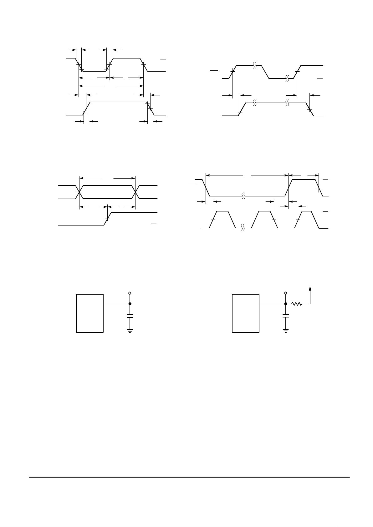
Figure 1. Figure 2.
10%
V+
GND
1/f
clk
OUTPUT A
(DATA OUT)
CLK
90%
50%
90%
50%
10%
t
PLH
t
PHL
t
TLH
t
THL
t
w
t
w
t
f
t
r
ENB
OUTPUT A
10%
V+
GND
50%
t
PLZ
50%
t
PZL
D
in
CLK
50%
VALID
50%
t
su
t
h
V+
GND
V+
GND
Figure 3.
CLK
ENB
50%
t
su
t
h
FIRST
CLOCK
LAST
CLOCK
t
rec
50%
V+
GND
V+
GND
t
w
t
w
Figure 4.
TEST POINT
DEVICE
UNDER
TEST
CL*
*Includes all probe and fixture capacitance.
TEST POINT
DEVICE
UNDER
TEST
CL*
*Includes all probe and fixture capacitance.
V+
7.5 k
Ω
Figure 5. Figure 6.

MC145220 MOTOROLA
6
LOOP SPECIFICATIONS (V+ = V+
i
= 2.7 to 5.5 V unless otherwise indicated, GND = GNDi, TA = – 40 to 85°C)
Guaranteed
Operating Range
Symbol Parameter Test Condition Min Max Unit
P
in
Input Sensitivity Range, fin or fini
(Figure 7)
40 MHz ≤ frequency < 300 MHz
300 MHz ≤ frequency < 700 MHz
700 MHz ≤ frequency < 1100 MHz
– 2
– 5
– 16
8
6
4
dBm*
∆P
in
Difference Allowed Between fin and fini
10 dB
—
Isolation Between fin and fini
15 dB
f
ref
Input Frequency, REFin Externally Driven in
Reference Mode (Figure 8)
Vin ≥ 400 mV p–p, R Counter set to divide
ratio such that fR ≤ 1 MHz, REF Counter set
to divide ratio such that REF
out
≤ 5 MHz
4 27
MHz
f
XTAL
Crystal Frequency, Crystal Mode (Figure 9) C1 ≤ 30 pF, C2 ≤ 30 pF, Includes Stray
Capacitance; R Counter and REF Counter
same as above V+ = 2.7 V
V+ = 3.5 V
V+ = 4.5 V
V+ = 5.5 V
2
2
2
2
10
13
15
15
MHz
f
out
Output Frequency, REF
out
(Figures 10 and 12) CL = 25 pF dc 5 MHz
f Operating Frequency of the Phase Detectors dc 1 MHz
t
w
Output Pulse Width, φR, φV, φRi
, φVi
(Figures 11 and 12)
fR in Phase with fV, CL = 25 pF 16 125 ns
C
in
Input Capacitance, REF
in
— 5 pF
*Power level at the input to the dc block.
MC145220MOTOROLA
7
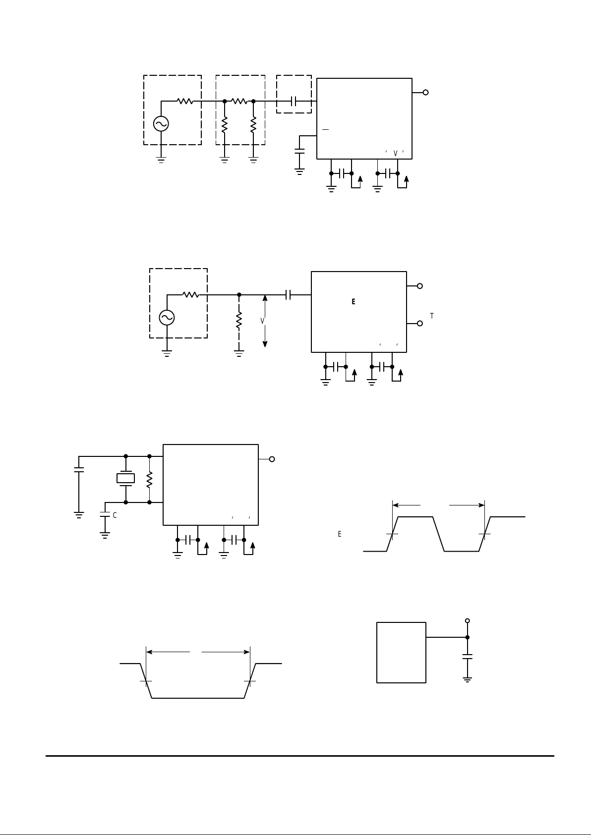
DEVICE
UNDER
TEST
TEST
POINT
f
in
OUTPUT A
Figure 7. Test Circuit
(fv)
Figure 8. Test Circuit — Reference Mode
DC
BLOCK
50
Ω
PAD
SINE WAVE
GENERAT OR
50
Ω
f
in
GND V+
GNDiV+
i
DEVICE
UNDER
TEST
TEST
POINT
REF
in
OUTPUT A
(fR)
0.01 µF
50
Ω
*
SINE WAVE
GENERAT OR
50
Ω
GND V+
GNDiV+
i
V
in
TEST
POINT
REF
out
*Characteristic Impedance
NOTE: Alternately, the 50 Ω pad may be a T network.
DEVICE
UNDER
TEST
TEST
POINT
REF
in
OUTPUT A
Figure 9. Test Circuit — Crystal Mode
(fR)
REF
out
GND V+
GNDiV+
i
C1
C2
REF
out
1/f
out
50%
Figure 10. Switching Waveform
OUTPUT
t
w
50%
Figure 11. Switching Waveform
TEST POINT
DEVICE
UNDER
TEST
CL*
*Includes all probe and fixture capacitance.
Figure 12. Test Circuit
MC145220 MOTOROLA
8
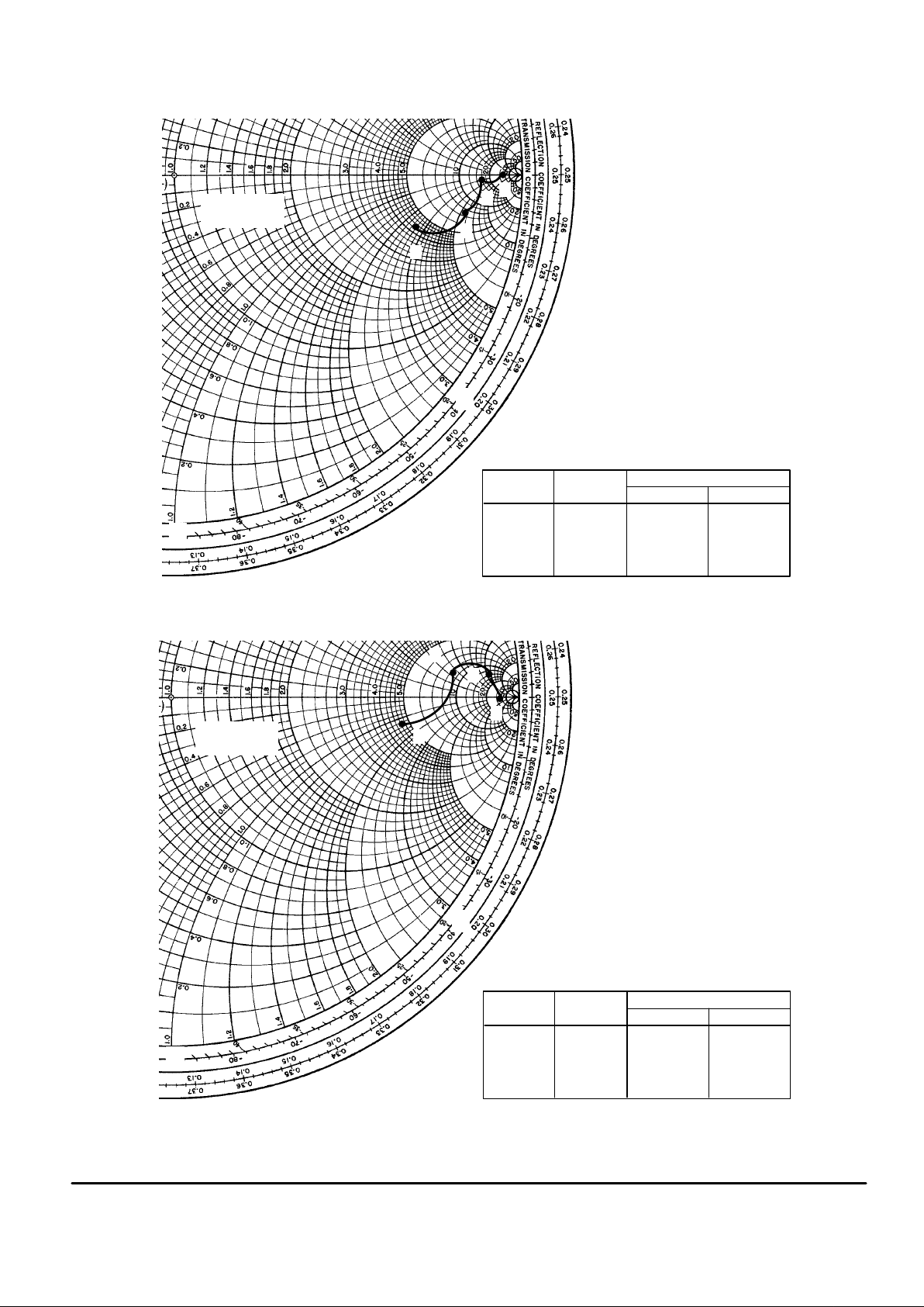
Frequency
(MHz)
Point
Impedance (Ω)
3 V Supply
5 V Supply
50
400
800
1100
E
F
G
H
1900 + j 149
878 + j 703
705 + j 208
215 – j 69.3
1930 + j 214
746 + j 741
626 + j 327
243 – j 61.3
Frequency
(MHz)
Point
Impedance (Ω)
3 V Supply
5 V Supply
50
400
800
1100
A
B
C
D
1900 – j 157
1440 – j 228
552 – j 380
196 – j 141
1970 – j 102
1510 + j 19
671 – j 334
223 – j 147
fin (PIN 8) – SOG PACKAGE
f
in
′
(PIN 13) – SOG PACKAGE
Figure 13. Nominal Input Impedance of fin and fin′ — Series Format (R + jX)
(50 – 1100 MHz)
–j2
–j1
A
B
C
D
fin (PIN 8)
SOG PACKAGE
–j2
–j1
E
F
G
H
fin′
(PIN 13)
SOG PACKAGE

MC145220MOTOROLA
9
PIN DESCRIPTIONS
DIGITAL INTERFACE PINS
D
in
Serial Data Input (Pin 20)
The bit stream begins with the MSB and is shifted in on the
low–to–high transition of CLK. The bit pattern is 1 byte (8
bits) long to access the C or configuration registers, 2 bytes
(16 bits) to access the first buffer of the R registers, or
3 bytes (24 bits) to access the A registers (see Table 1). The
values in the registers do not change during shifting because
the transfer of data to the registers is controlled by ENB
.
NOTE
The value programmed for the N counter must be
greater than or equal to the value of the A counter.
The 13 LSBs of the R registers are double–buffered. As indicated above, data is latched into the first buffer on a 16–bit
transfer. (The 3 MSBs are not double–buffered and have an
immediate effect after a 16–bit transfer.) The two second
buffers of the R register contain the two 13–bit divide ratios
for the R counters. These second buffers are loaded with the
contents of the first buffer as follows. Whenever the A register is loaded, the Rs (second) buffer is loaded from the R
(first) buffer . Similarly , whenever the Ai register is loaded, the
Rsi (second) buffer is updated from the R (first) buffer. This
allows presenting new values to the R, A, and N counters
simultaneously. Note that two different R counter divide
ratios may be established: one for the main PLL and another
for PLLi.
The bit stream does not need address bits due to the innovative BitGrabber Plus registers. A steering bit is used to
direct data to either the main PLL or PLLi section of the chip.
Data is retained in the registers over a supply range of 2.7 to
5.5 V. The formats are shown in Figures 14, 15, and 16.
Din typically switches near 50% of V+ to maximize noise
immunity. This input can be directly interfaced to CMOS
devices with outputs guaranteed to switch near rail–to–rail.
When interfacing to NMOS or TTL devices, either a level
shifter (MC74HC14A, MC14504B) or pull–up resistor of 1 kΩ
to 10 kΩ must be used. Parameters to consider when sizing
the resistor are worst–case IOL of the driving device, maximum tolerable power consumption, and maximum data rate.
Table 1. Register Access
(MSBs are shifted in first; C0, R0, and A0 are the LSBs)
Number
of Clocks
Accessed
Register
Bit
Nomenclature
8
16
24
Other Values ≤ 32
Values > 32
C Registers
R Register,
First Buffer
A Registers
Not Allowed
See Figures
24 to 27
C7, C6, C5, . . ., C0
R15, R14, R13, . . ., R0
A23, A22, A21, . . ., A0
CLK
Serial Data Clock Input (Pin 19)
Low–to–high transitions on CLK shift bits available at the
Din pin, while high–to–low transitions shift bits from Output A
(when configured as Data Out, see Pin 10). The 24–1/2
stage shift register is static, allowing clock rates down to dc in
a continuous or intermittent mode.
Eight clock cycles are required to access the C registers.
Sixteen clock cycles are needed for the first buffer of the R
register. Twenty–four cycles are used to access the A registers. See Table 1 and Figures 14, 15, and 16. The number of
clocks required for cascaded devices is shown in Figures 25
through 27.
CLK typically switches near 50% of V+ and has a Schmitt–
triggered input buffer. Slow CLK rise and fall times are allowed. See the last paragraph of Din for more information.
NOTE
To guarantee proper operation of the power–on
reset (POR) circuit, the CLK pin must be held at
GND (with ENB
being a don’t care) or ENB must
be held at the potential of the V+ pin (with CLK being a don’t care) during power–up. Floating, toggling, or having these pins in the wrong state
during power–up does not harm the chip, but
causes two potentially undesirable effects. First,
the outputs of the device power up in an unknown
state. Second, if two devices are cascaded, the A
Registers must be written twice after power up.
After these two accesses, the two cascaded chips
perform normally .
ENB
Active–Low Enable Input (Pin 11)
This pin is used to activate the serial interface to allow the
transfer of data to/from the device. When ENB
is in an inactive high state, shifting is inhibited and the port is held in the
initialized state. To transfer data to the device, ENB
(which
must start inactive high) is taken low, a serial transfer is
made via Din and CLK, and ENB
is taken back high. The
low–to–high transition on ENB transfers data to the C or A
registers and first buffer of the R register, depending on the
data stream length per Table 1.
NOTE
Transitions on ENB
must not be attempted while
CLK is high. This puts the device out of synchronization with the microcontroller. Resynchronization occurs whenever ENB
is high and CLK is
low.
This input is Schmitt–triggered and switches near 50% of
V+, thereby minimizing the chance of loading erroneous data
into the registers. See the last paragraph of Din for more
information.
For POR information, see the note for the CLK pin.
 Loading...