

Motorola MC14521BCL, MC14521BCP, MC14521BD Datasheet
MOTOROLA CMOS LOGIC DATA
1
MC14521B
" !
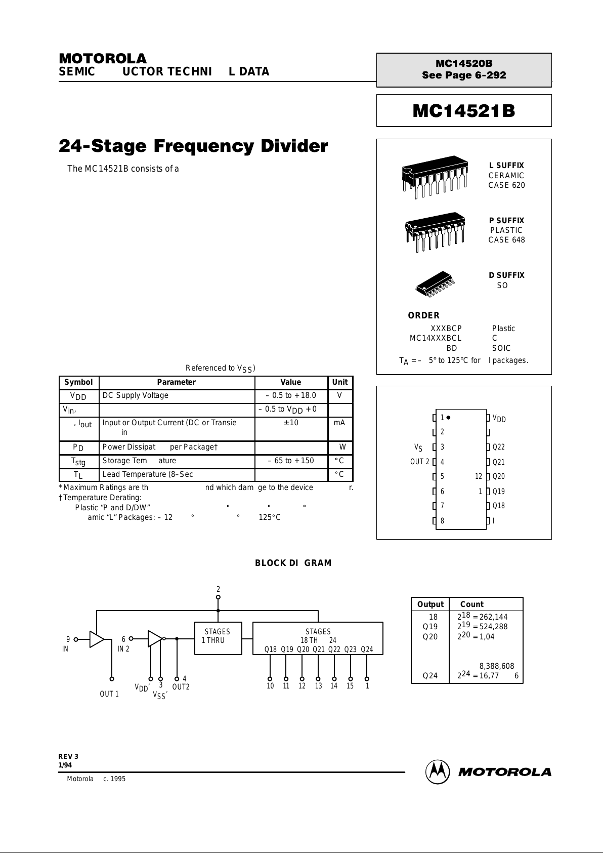
The MC14521B consists of a chain of 24 flip–flops with an input circuit that
allows three modes of operation. The i nput will function as a crystal
oscillator, an RC oscillator, or as an input buffer for an external oscillator.
Each flip–flop divides the frequency of t he previous flip–flop by two,
consequently this part will count up to 224 = 16,777,216. The count advances
on the n egative g oing e dge o f the c lock. T he outputs o f the l ast
seven–stages are available for added flexibility.
• All Stages are Resettable
• Reset Disables the RC Oscillator for Low Standby Power Drain
• RC and Crystal Oscillator Outputs Are Capable of Driving External
Loads
• Test Mode to Reduce Test Time
• VDD′ and VSS′ Pins Brought Out on Crystal Oscillator Inverter to Allow
the Connection of External Resistors for Low–Power Operation
• Supply Voltage Range = 3.0 Vdc to 18 Vdc
• Capable of Driving Two Low–power TTL Loads or One Low–power
Schottky TTL Load over the Rated Temperature Range.
MAXIMUM RATINGS* (Voltages Referenced to V
SS
)
Symbol
Parameter
Value
Unit
V
DD
DC Supply Voltage
– 0.5 to + 18.0
V
Vin, V
out
Input or Output Voltage (DC or Transient)
– 0.5 to VDD + 0.5
V
Iin, I
out
Input or Output Current (DC or Transient),
per Pin
± 10
mA
P
D
Power Dissipation, per Package†
500
mW
T
stg
Storage Temperature
– 65 to + 150
_
C
T
L
Lead Temperature (8–Second Soldering)
260
_
C
*Maximum Ratings are those values beyond which damage to the device may occur.
†Temperature Derating:
Plastic “P and D/DW” Packages: – 7.0 mW/_C From 65_C To 125_C
Ceramic “L” Packages: – 12 mW/_C From 100_C To 125_C
BLOCK DIAGRAM
Output Count Capacity
Q18 218 = 262,144
Q19 219 = 524,288
Q20 220 = 1,048,576
Q21 221 = 2,097,152
Q22 222 = 4,194,304
Q23 223 = 8,388,608
Q24 224 = 16,777,216
STAGES
18 THRU 24
STAGES
1 THRU 17
Q18 Q19 Q20 Q21 Q22 Q23 Q24
10 11 12 13 14 15 1
2
6
IN 2
9
IN 1
7
RESET
VDD = PIN 16
VSS = PIN 8
5
3
4
OUT 1
V
DD
′
VSS′
OUT2
SEMICONDUCTOR TECHNICAL DATA
Motorola, Inc. 1995
REV 3
1/94
L SUFFIX
CERAMIC
CASE 620
ORDERING INFORMATION
MC14XXXBCP Plastic
MC14XXXBCL Ceramic
MC14XXXBD SOIC
TA = – 55° to 125°C for all packages.
P SUFFIX
PLASTIC
CASE 648
D SUFFIX
SOIC
CASE 751B
PIN ASSIGNMENT
13
14
15
16
9
10
11
125
4
3
2
1
8
7
6
Q20
Q21
Q22
V
DD
IN 1
Q18
Q19
OUT 2
V
SS
′
RESET
Q24
V
SS
OUT 1
IN 2
V
DD
′
Q23
MOTOROLA CMOS LOGIC DATAMC14521B
2
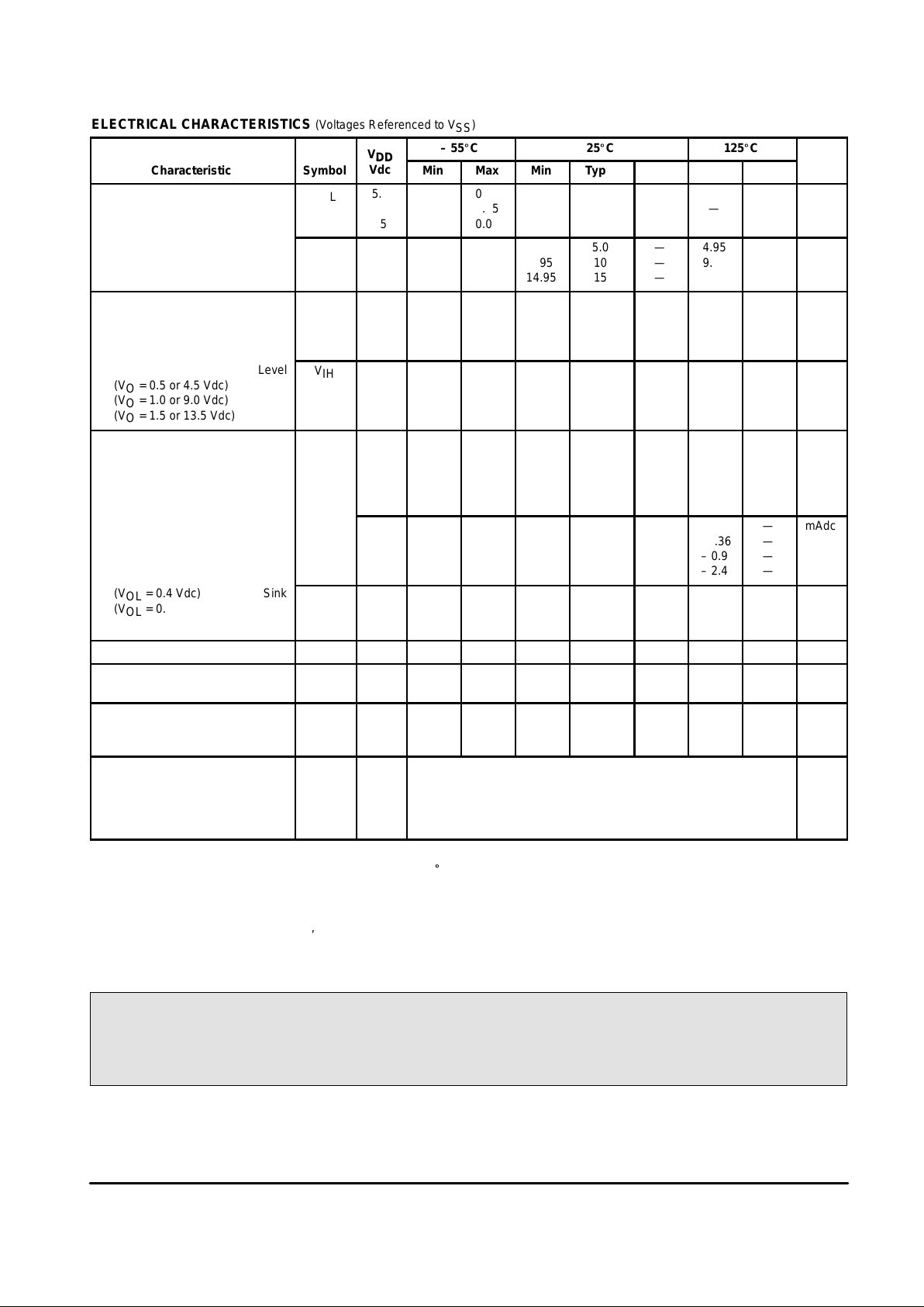
ELECTRICAL CHARACTERISTICS (Voltages Referenced to V
SS
)
V
– 55_C 25_C 125_C
Characteristic
Symbol
V
DD
Vdc
Min Max Min Typ # Max Min Max
Unit
Output Voltage
“0” Level
Vin = VDD or 0
V
OL
5.0
10
15
—
—
—
0.05
0.05
0.05
—
—
—
0
0
0
0.05
0.05
0.05
—
—
—
0.05
0.05
0.05
Vdc
“1” Level
Vin = 0 or V
DD
V
OH
5.0
10
15
4.95
9.95
14.95
—
—
—
4.95
9.95
14.95
5.0
10
15
—
—
—
4.95
9.95
14.95
—
—
—
Vdc
Input Voltage
“0” Level
(VO = 4.5 or 0.5 Vdc)
(VO = 9.0 or 1.0 Vdc)
(VO = 13.5 or 1.5 Vdc)
V
IL
5.0
10
15
—
—
—
1.5
3.0
4.0
—
—
—
2.25
4.50
6.75
1.5
3.0
4.0
—
—
—
1.5
3.0
4.0
Vdc
“1” Level
(VO = 0.5 or 4.5 Vdc)
(VO = 1.0 or 9.0 Vdc)
(VO = 1.5 or 13.5 Vdc)
V
IH
5.0
10
15
3.5
7.0
11
—
—
—
3.5
7.0
11
2.75
5.50
8.25
—
—
—
3.5
7.0
11
—
—
—
Vdc
Output Drive Current
(VOH = 2.5 Vdc) Source
(VOH = 4.6 Vdc) Pins 4 & 7
(VOH = 9.5 Vdc)
(VOH = 13.5 Vdc)
I
OH
5.0
5.0
10
15
– 1.2
– 0.25
– 0.62
– 1.8
—
—
—
—
– 1.0
– 0.2
– 0.5
– 1.5
– 1.7
– 0.36
– 0.9
– 3.5
—
—
—
—
– 0.7
– 0.14
– 0.35
– 1.1
—
—
—
—
mAdc
(VOH = 2.5 Vdc) Source
(VOH = 4.6 Vdc)
Pins 1, 10,
(VOH = 9.5 Vdc) 11, 12, 13, 14
(VOH = 13.5 Vdc) and 15
5.0
5.0
10
15
– 3.0
– 0.64
– 1.6
– 4.2
—
—
—
—
– 2.4
– 0.51
– 1.3
– 3.4
– 4.2
– 0.88
– 2.25
– 8.8
—
—
—
—
– 1.7
– 0.36
– 0.9
– 2.4
—
—
—
—
mAdc
(VOL = 0.4 Vdc) Sink
(VOL = 0.5 Vdc)
(VOL = 1.5 Vdc)
I
OL
5.0
10
15
0.64
1.6
4.2
—
—
—
0.51
1.3
3.4
0.88
2.25
8.8
—
—
—
0.36
0.9
2.4
—
—
—
mAdc
Input Current I
in
15 — ± 0.1 — ±0.00001 ± 0.1 — ± 1.0 µAdc
Input Capacitance
(Vin = 0)
C
in
— — — — 5.0 7.5 — — pF
Quiescent Current
(Per Package)
I
DD
5.0
10
15
—
—
—
5.0
10
20
—
—
—
0.005
0.010
0.015
5.0
10
20
—
—
—
150
300
600
µAdc
Total Supply Current**†
(Dynamic plus Quiescent,
Per Package)
(CL = 50 pF on all outputs, all
buffers switching)
I
T
5.0
10
15
IT = (0.42 µA/kHz) f + I
DD
IT = (0.85 µA/kHz) f + I
DD
IT = (1.40 µA/kHz) f + I
DD
µAdc
#Data labelled “Typ” is not to be used for design purposes but is intended as an indication of the IC’s potential performance.
**The formulas given are for the typical characteristics only at 25_C.
†To calculate total supply current at loads other than 50 pF:
IT(CL) = IT(50 pF) + (CL – 50) Vfk
where: IT is in µA (per package), CL in pF, V = (VDD – VSS) in volts, f in kHz is input frequency, and k = 0.003.
This device contains protection circuitry to guard against damage due to high static voltages or electric fields. However,
precautions must be taken to avoid applications of any voltage higher than maximum rated voltages to this high-impedance
circuit. For proper operation, Vin and V
out
should be constrained to the range VSS ≤ (Vin or V
out
) ≤ VDD.
Unused inputs must always be tied to an appropriate logic voltage level (e.g., either VSS or VDD). Unused outputs must
be left open.
MOTOROLA CMOS LOGIC DATA
3
MC14521B
SWITCHING CHARACTERISTICS* (C
L
= 50 pF, TA = 25_C)
Characteristic
Symbol
V
DD
Vdc
Min Typ # Max Unit
Output Rise and Fall Time (Counter Outputs)
t
TLH
, t
THL
= (1.5 ns/pF) CL + 25 ns
t
TLH
, t
THL
= (0.75 ns/pF) CL + 12.5 ns
t
TLH
, t
THL
= (0.55 ns/pF) CL + 12.5 ns
t
TLH
, t
THL
5.0
10
15
—
—
—
100
50
40
200
100
80
ns
Propagation Delay Time
Clock to Q18
t
PHL
, t
PLH
= (1.7 ns/pF) CL + 4415 ns
t
PHL
, t
PLH
= (0.66 ns/pF) CL + 1667 ns
t
PHL
, t
PLH
= (0.5 ns/pF) CL + 1275 ns
t
PHL
, t
PLH
5.0
10
15
—
—
—
4.5
1.7
1.3
9.0
3.5
2.7
µs
Clock to Q24
t
PHL
, t
PLH
= (1.7 ns/pF) CL + 5915 ns
t
PHL
, t
PLH
= (0.66 ns/pF) CL + 2167 ns
t
PHL
, t
PLH
= (0.5 ns/pF) CL + 1675 ns
5.0
10
15
—
—
—
6.0
2.2
1.7
12
4.5
3.5
Propagation Delay Time
Reset to Q
n
t
PHL
= (1.7 ns/pF) CL + 1215 ns
t
PHL
= (0.66 ns/pF) CL + 467 ns
t
PHL
= (0.5 ns/pF) CL + 350 ns
t
PHL
5.0
10
15
—
—
—
1300
500
375
2600
1000
750
ns
Clock Pulse Width t
WH(cl)
5.0
10
15
385
150
120
140
55
40
—
—
—
ns
Clock Pulse Frequency f
cl
5.0
10
15
—
—
—
3.5
9.0
12
2.0
5.0
6.5
MHz
Clock Rise and Fall Time t
TLH
, t
THL
5.0
10
15
—
—
—
—
—
—
15
5.0
4.0
µs
Reset Pulse Width t
WH(R)
5.0
10
15
1400
600
450
700
300
225
—
—
—
ns
Reset Removal Time t
rem
5.0
10
15
30
0
– 40
– 200
– 160
– 110
—
—
—
ns
*The formulas given are for the typical characteristics only at 25_C.
#Data labelled “Typ” is not to be used for design purposes but is intended as an indication of the IC’s potential performance.
Figure 1. Power Dissipation Test Circuit and Waveform
PULSE
GENERATOR
V
DD
V
DD
V
DD
V
SS
V
SS
Q18
Q19
Q20
Q21
Q22
Q23
Q24
C
L
C
L
C
L
C
L
C
L
C
L
C
L
I
D
IN 2
R
500
µ
F
0.01 µF
CERAMIC
20 ns 20 ns
V
DD
0 V
V
in
50% DUTY CYCLE
90%
10%
50%
 Loading...