

Motorola MC14050UBCL, MC14050UBCP, MC14050UBD Datasheet
MOTOROLA CMOS LOGIC DATA
1
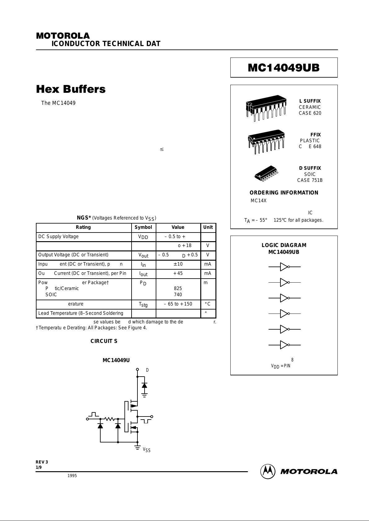
MC14049UB
The MC14049UB hex inverter/buffer is constructed with MOS P–channel
and N–channel enhancement mode devices in a single monolithic structure.
This complementary MOS d evice f inds primary use where low power
dissipation and/or high noise immunity is desired. This device provides
logic–level conversion using only one supply voltage, VDD. The input–signal
high l evel (VIH) can exceed the VDD supply v oltage for logic–level
conversions. Two TTL/DTL Loads can be driven when the device is used as
CMOS–to–TTL/DTL converters (VDD = 5.0 V, VOL v 0.4 V, IOL ≥ 3.2 mA).
Note t hat pins 13 a nd 16 are not connected internally on t his device;
consequently connections to these terminals will not affect circuit operation.
• High Source and Sink Currents
• High–to–Low Level Converter
• Supply Voltage Range = 3.0 V to 18 V
• Meets JEDEC UB Specifications
• VIN can exceed V
DD
• Improved ESD Protection on All Inputs
MAXIMUM RATINGS* (Voltages Referenced to V
SS
)
Rating
Symbol
Value
Unit
DC Supply Voltage
V
DD
– 0.5 to + 18
V
Input Voltage (DC or Transient)
V
in
– 0.5 to + 18
V
Output Voltage (DC or Transient)
V
out
– 0.5 to VDD + 0.5
V
Input Current (DC or Transient), per Pin
I
in
± 10
mA
Output Current (DC or Transient), per Pin
I
out
+ 45
mA
Power Dissipation, per Package†
Plastic/Ceramic
SOIC
P
D
825
740
mW
Storage Temperature
T
stg
– 65 to + 150
_
C
Lead Temperature (8–Second Soldering)
T
L
260
_
C
*Maximum Ratings are those values beyond which damage to the device may occur.
†Temperature Derating: All Packages: See Figure 4.
CIRCUIT SCHEMATIC
(1/6 OF CIRCUIT SHOWN)
V
DD
V
SS
MC14049UB
SEMICONDUCTOR TECHNICAL DATA
Motorola, Inc. 1995
REV 3
1/94
L SUFFIX
CERAMIC
CASE 620
ORDERING INFORMATION
MC14XXXBCP Plastic
MC14XXXBCL Ceramic
MC14XXXBD SOIC
TA = – 55° to 125°C for all packages.
P SUFFIX
PLASTIC
CASE 648
D SUFFIX
SOIC
CASE 751B
LOGIC DIAGRAM
MC14049UB
14 15
11
9
7
5
3
12
10
6
4
2
NC = PIN 13, 16
VSS = PIN 8
VDD = PIN 1
MOTOROLA CMOS LOGIC DATAMC14049UB
2
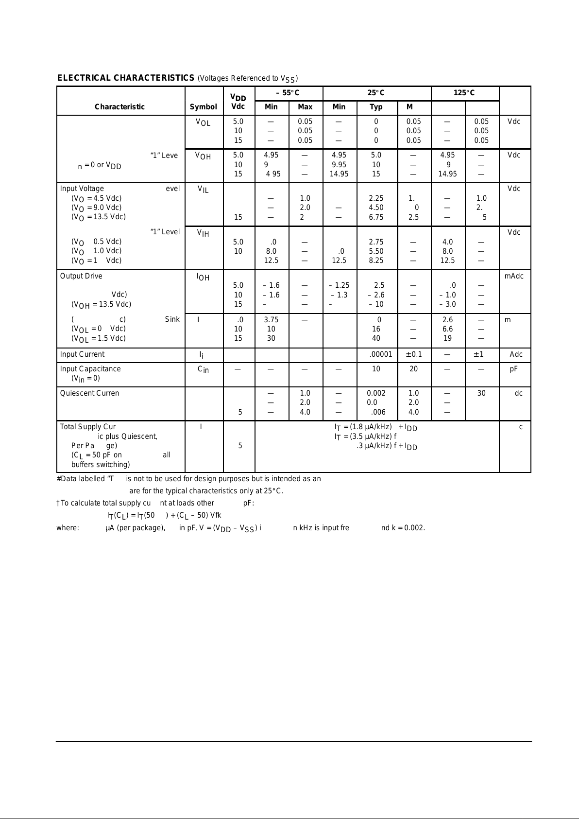
ELECTRICAL CHARACTERISTICS (Voltages Referenced to V
SS
)
V
– 55_C
25_C
125_C
Characteristic
Symbol
V
DD
Vdc
Min
Max
Min
Typ
Max
Min
ÎÎÎ
ÎÎÎ
ÎÎÎ
Max
Unit
Output Voltage
“0” Level
Vin = VDD or 0
V
OL
5.0
10
15
—
—
—
0.05
0.05
0.05
—
—
—
0
0
0
0.05
0.05
0.05
—
—
—
ÎÎÎ
ÎÎÎ
ÎÎÎ
ÎÎÎ
0.05
0.05
0.05
Vdc
“1” Level
Vin = 0 or V
DD
V
OH
5.0
10
15
4.95
9.95
14.95
—
—
—
4.95
9.95
14.95
5.0
10
15
—
—
—
4.95
9.95
14.95
ÎÎÎ
ÎÎÎ
ÎÎÎ
ÎÎÎ
ÎÎÎ
—
—
—
Vdc
Input Voltage
“0” Level
(VO = 4.5 Vdc)
(VO = 9.0 Vdc)
(VO = 13.5 Vdc)
V
IL
5.0
10
15
—
—
—
1.0
2.0
2.5
—
—
—
2.25
4.50
6.75
1.0
2.0
2.5
—
—
—
ÎÎÎ
ÎÎÎ
ÎÎÎ
ÎÎÎ
ÎÎÎ
1.0
2.0
2.5
Vdc
“1” Level
(VO = 0.5 Vdc)
(VO = 1.0 Vdc)
(VO = 1.5 Vdc)
V
IH
5.0
10
15
4.0
8.0
12.5
—
—
—
4.0
8.0
12.5
2.75
5.50
8.25
—
—
—
4.0
8.0
12.5
ÎÎÎ
ÎÎÎ
ÎÎÎ
ÎÎÎ
ÎÎÎ
—
—
—
Vdc
Output Drive Current
(VOH = 2.5 Vdc) Source
(VOH = 9.5 Vdc)
(VOH = 13.5 Vdc)
I
OH
5.0
10
15
– 1.6
– 1.6
– 4.7
—
—
—
– 1.25
– 1.3
– 3.75
– 2.5
– 2.6
– 10
—
—
—
– 1.0
– 1.0
– 3.0
ÎÎÎ
ÎÎÎ
ÎÎÎ
ÎÎÎ
ÎÎÎ
—
—
—
mAdc
(VOL = 0.4 Vdc) Sink
(VOL = 0.5 Vdc)
(VOL = 1.5 Vdc)
I
OL
5.0
10
15
3.75
10
30
—
—
—
3.2
8.0
24
6.0
16
40
—
—
—
2.6
6.6
19
ÎÎÎ
ÎÎÎ
ÎÎÎ
ÎÎÎ
—
—
—
mAdc
Input Current
I
in
15
—
± 0.1
—
±0.00001
± 0.1
—
ÎÎÎ
ÎÎÎ
ÎÎÎ
± 1.0
µAdc
Input Capacitance
(Vin = 0)
C
in
—
—
—
—
10
20
—
ÎÎÎ
ÎÎÎ
ÎÎÎ
ÎÎÎ
—
pF
Quiescent Current
(Per Package)
I
DD
5.0
10
15
—
—
—
1.0
2.0
4.0
—
—
—
0.002
0.004
0.006
1.0
2.0
4.0
—
—
—
ÎÎÎ
ÎÎÎ
ÎÎÎ
ÎÎÎ
30
60
120
µAdc
Total Supply Current**†
(Dynamic plus Quiescent,
Per Package)
(CL = 50 pF on all outputs, all
buffers switching)
I
T
5.0
10
15
IT = (1.8 µA/kHz) f + I
DD
IT = (3.5 µA/kHz) f + I
DD
IT = (5.3 µA/kHz) f + I
DD
µAdc
#Data labelled “Typ” is not to be used for design purposes but is intended as an indication of the IC’s potential performance.
**The formulas given are for the typical characteristics only at 25_C.
†To calculate total supply current at loads other than 50 pF:
IT(CL) = IT(50 pF) + (CL – 50) Vfk
where: IT is in µA (per package), CL in pF, V = (VDD – VSS) in volts, f in kHz is input frequency, and k = 0.002.
 Loading...