

MOTOROLA MC14050BFEL, MC14050BFL1, MC14050BFL2, MC14050BFR1, MC14050BFR2 Datasheet
...
Semiconductor Components Industries, LLC, 2000
March, 2000 – Rev. 3
1 Publication Order Number:
MC14049B/D
MC14049B, MC14050B
Hex Buffer
The MC14049B Hex Inverter/Buffer and MC14050B Noninverting
Hex Buffer are constructed with MOS P–Channel and N–Channel
enhancement mode devices in a single monolithic structure. These
complementary MOS devices find primary use where low power
dissipation and/or high noise immunity is desired. These devices
provide logic level conversion using only one supply voltage, V
DD
.
The input–signal high level (VIH) can exceed the VDD supply
voltage for logic level conversions. T wo TTL/DTL loads can be driven
when the devices are used as a CMOS–to–TTL/DTL converter (V
DD
= 5.0 V, VOL v 0.4 V, IOL ≥ 3.2 mA).
Note that pins 13 and 16 are not connected internally on these
devices; consequently connections to these terminals will not affect
circuit operation.
• High Source and Sink Currents
• High–to–Low Level Converter
• Supply Voltage Range = 3.0 V to 18 V
• V
IN
can exceed V
DD
• Meets JEDEC B Specifications
• Improved ESD Protection On All Inputs
MAXIMUM RATINGS (Voltages Referenced to V
SS
) (Note 2.)
Symbol
Parameter Value Unit
V
DD
DC Supply Voltage Range –0.5 to +18.0 V
V
in
Input Voltage Range
(DC or Transient)
–0.5 to +18.0 V
V
out
Output Voltage Range
(DC or Transient)
–0.5 to VDD + 0.5 V
I
in
Input Current
(DC or Transient) per Pin
±10 mA
I
out
Output Current
(DC or Transient) per Pin
±45 mA
P
D
Power Dissipation,
per Package (Note 3.)
(Plastic)
(SOIC)
825
740
mW
T
A
Ambient Temperature Range –55 to +125 °C
T
stg
Storage Temperature Range –65 to +150 °C
T
L
Lead Temperature
(8–Second Soldering)
260 °C
2. Maximum Ratings are those values beyond which damage to the device
may occur.
3. Temperature Derating: See Figure 3.
This device contains protection circuitry to protect the inputs against damage
due to high static voltages or electric fields referenced to the V
SS
pin only. Extra
precautions must be taken to avoid applications of any voltage higher than the
maximum rated voltages to this high–impedance circuit. For proper operation, the
ranges V
SS
≤ Vin ≤ 18 V and VSS ≤ V
out
≤ V
DD
are recommended.
Unused inputs must always be tied to an appropriate logic voltage level (e.g.,
either V
SS
or VDD). Unused outputs must be left open.
http://onsemi.com
XX = Specific Device Code
A = Assembly Location
WL or L = Wafer Lot
YY or Y = Year
WW or W = Work Week
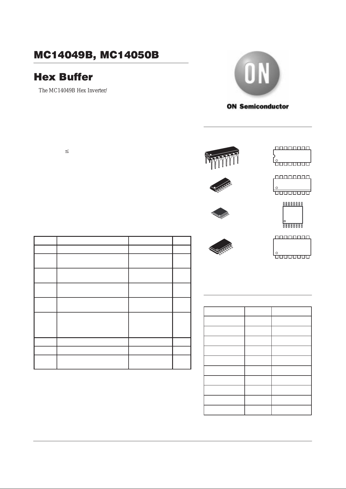
Device Package Shipping
ORDERING INFORMATION
MC14049BCP PDIP–16 2000/Box
MC14049BD SOIC–16 2400/Box
MC14049BDR2 SOIC–16 2500/Tape & Reel
1. For ordering information on the EIAJ version of
the SOIC packages, please contact your local
ON Semiconductor representative.
MARKING
DIAGRAMS
1
16
PDIP–16
P SUFFIX
CASE 648
MC140XXBCP
AWLYYWW
SOIC–16
D SUFFIX
CASE 751B
1
16
140XXB
AWLYWW
SOEIAJ–16
F SUFFIX
CASE 966
1
16
MC140XXB
AWLYWW
MC14049BF SOEIAJ–16 See Note 1.
MC14050BCP PDIP–16 2000/Box
MC14050BD SOIC–16 2400/Box
MC14050BDR2 SOIC–16 2500/Tape & Reel
MC14050BDTEL TSSOP–16 2000/Tape & Reel
MC14050BF SOEIAJ–16 See Note 1.
MC14050BFEL SOEIAJ–16 See Note 1.
TSSOP–16
DT SUFFIX
CASE 948F
14
0XXB
ALYW
1
16
MC14049B, MC14050B
http://onsemi.com
2
PIN ASSIGNMENT
13
14
15
16
9
10
11
125
4
3
2
1
8
7
6
OUT
E
NC
IN
F
OUT
F
NC
IN
D
OUT
D
IN
E
OUT
B
IN
A
OUT
A
V
DD
V
SS
IN
C
OUT
C
IN
B
LOGIC DIAGRAM
MC14049B
14 15
11
9
7
5
3
12
10
6
4
2
NC = PIN 13, 16
V
SS
= PIN 8
V
DD
= PIN 1
MC14050B
14 15
11
9
7
5
3
12
10
6
4
2
NC = PIN 13, 16
V
SS
= PIN 8
V
DD
= PIN 1
MC14049B, MC14050B
http://onsemi.com
3
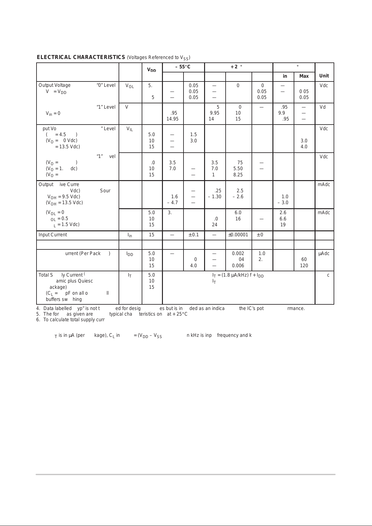
ELECTRICAL CHARACTERISTICS (Voltages Referenced to V
SS
)
V
– 55_C
+ 25_C
+ 125_C
Characteristic
Symbol
V
DD
Vdc
Min
Max
Min
Typ
(4.)
Max
Min
Max
Unit
ОООООООО
Î
Output Voltage “0” Level
V
in
= V
DD
ÎÎ
Î
V
OL
Î
Î
5.0
10
15
Î
Î
—
—
—
Î
Î
0.05
0.05
0.05
ÎÎ
Î
—
—
—
Î
Î
0
0
0
ÎÎ
Î
0.05
0.05
0.05
Î
Î
—
—
—
Î
Î
0.05
0.05
0.05
Î
Î
Vdc
ОООООООО
Î
“1” Level
V
in
= 0
ÎÎ
Î
V
OH
Î
Î
5.0
10
15
Î
Î
4.95
9.95
14.95
Î
Î
—
—
—
ÎÎ
Î
4.95
9.95
14.95
Î
Î
5.0
10
15
ÎÎ
Î
—
—
—
Î
Î
4.95
9.95
14.95
Î
Î
—
—
—
Î
Î
Vdc
ОООООООО
Î
ОООООООО
Î
Input Voltage “0” Level
(V
O
= 4.5 Vdc)
(V
O
= 9.0 Vdc)
(V
O
= 13.5 Vdc)
ÎÎ
Î
ÎÎ
Î
V
IL
Î
Î
Î
Î
5.0
10
15
Î
Î
Î
Î
—
—
—
Î
Î
Î
Î
1.5
3.0
4.0
ÎÎ
Î
ÎÎ
Î
—
—
—
Î
Î
Î
Î
2.25
4.50
6.75
ÎÎ
Î
ÎÎ
Î
1.5
3.0
4.0
Î
Î
Î
Î
—
—
—
Î
Î
Î
Î
1.5
3.0
4.0
Î
Î
Î
Î
Vdc
ОООООООО
Î
ОООООООО
Î
“1” Level
(V
O
= 0.5 Vdc)
(V
O
= 1.0 Vdc)
(V
O
= 1.5 Vdc)
ÎÎ
Î
ÎÎ
Î
V
IH
Î
Î
Î
Î
5.0
10
15
Î
Î
Î
Î
3.5
7.0
11
Î
Î
Î
Î
—
—
—
ÎÎ
Î
ÎÎ
Î
3.5
7.0
11
Î
Î
Î
Î
2.75
5.50
8.25
ÎÎ
Î
ÎÎ
Î
—
—
—
Î
Î
Î
Î
3.5
7.0
11
Î
Î
Î
Î
—
—
—
Î
Î
Î
Î
Vdc
ОООООООО
Î
ОООООООО
Î
Output Drive Current
(V
OH
= 2.5 Vdc) Source
(V
OH
= 9.5 Vdc)
(V
OH
= 13.5 Vdc)
ÎÎ
Î
ÎÎ
Î
I
OH
Î
Î
Î
Î
5.0
10
15
Î
Î
Î
Î
– 1.6
– 1.6
– 4.7
Î
Î
Î
Î
—
—
—
ÎÎ
Î
ÎÎ
Î
– 1.25
– 1.30
– 3.75
Î
Î
Î
Î
– 2.5
– 2.6
– 10
ÎÎ
Î
ÎÎ
Î
—
—
—
Î
Î
Î
Î
– 1.0
– 1.0
– 3.0
Î
Î
Î
Î
—
—
—
Î
Î
Î
Î
mAdc
ОООООООО
Î
ОООООООО
Î
(VOL = 0.4 Vdc) Sink
(V
OL
= 0.5 Vdc)
(V
OL
= 1.5 Vdc)
ÎÎ
Î
ÎÎ
Î
I
OL
Î
Î
Î
Î
5.0
10
15
Î
Î
Î
Î
3.75
10
30
Î
Î
Î
Î
—
—
—
ÎÎ
Î
ÎÎ
Î
3.2
8.0
24
Î
Î
Î
Î
6.0
16
40
ÎÎ
Î
ÎÎ
Î
—
—
Î
Î
Î
Î
2.6
6.6
19
Î
Î
Î
Î
—
—
—
Î
Î
Î
Î
mAdc
Input Current
I
in
15
—
± 0.1
—
±0.00001
± 0.1
—
± 1.0
µAdc
Input Capacitance (Vin = 0)
C
in
—
—
—
—
10
20
—
—
pF
ОООООООО
Î
Quiescent Current (Per Package)
ÎÎ
Î
I
DD
Î
Î
5.0
10
15
Î
Î
—
—
—
Î
Î
1.0
2.0
4.0
ÎÎ
Î
—
—
—
Î
Î
0.002
0.004
0.006
ÎÎ
Î
1.0
2.0
4.0
Î
Î
—
—
—
Î
Î
30
60
120
Î
Î
µAdc
ОООООООО
Î
ОООООООО
Î
ОООООООО
Î
Total Supply Current
(5.) (6.)
(Dynamic plus Quiescent,
per package)
(C
L
= 50 pF on all outputs, all
buffers switching
ÎÎ
Î
ÎÎ
Î
ÎÎ
Î
I
T
Î
Î
Î
Î
Î
Î
5.0
10
15
ООООООООООООООО
Î
ООООООООООООООО
Î
ООООООООООООООО
Î
IT = (1.8 µA/kHz) f + I
DD
IT = (3.5 µA/kHz) f + I
DD
IT = (5.3 µA/kHz) f + I
DD
Î
Î
Î
Î
Î
Î
µAdc
4. Data labelled “Typ” is not to be used for design purposes but is intended as an indication of the IC’s potential performance.
5. The formulas given are for the typical characteristics only at + 25_C
6. To calculate total supply current at loads other than 50 pF:
I
T(CL
) = IT(50 pF) + (CL – 50) Vfk
Where:
I
T
is in µA (per Package), CL in pF, V = (VDD – VSS) in volts, f in kHz is input frequency and k = 0.002.
 Loading...