

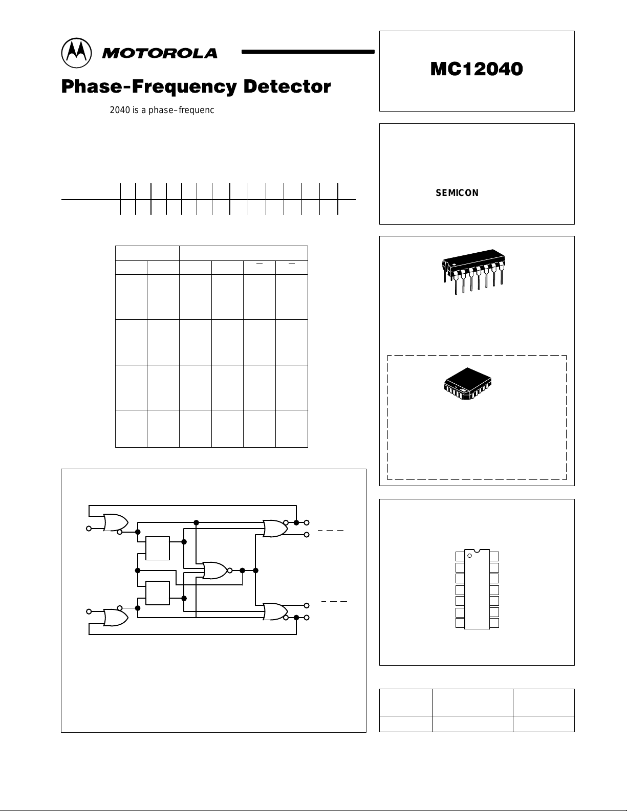
Motorola MC12040FN, MC12040P Datasheet
The MC12040 is a phase–frequency detector intended for use in systems
requiring zero phase and frequency difference at lock. In combination with a
voltage controlled oscillator (such as the MC1648, MC12147, MC12148 or
MC12149), it is useful in a broad range of phase–locked loop applications.
• Operating Frequency = 80 MHz Typical
Pin Conversion T able
14 PIN DIP 1 2 3 4 5 6 7 8 9 10 11 12 13 14
20 PIN PLCC 2 3 4 6 8 9 10 12 13 14 16 18 19 20
Order this document by MC12040/D
PHASE–FREQUENCY
DETECTOR
SEMICONDUCTOR
TECHNICAL DATA
Inputs
R
0
0
1
0
1
0
1
1
1
1
1
1
1
0
1
V
0
1
1
1
1
1
1
0
1
0
1
0
1
1
1
U
X
X
X
X
1
1
1
1
0
0
0
0
0
0
0
Outputs
D
X
X
X
X
0
0
0
0
0
0
1
1
1
1
0
U
X
X
X
X
0
0
0
0
1
1
1
1
1
1
1
D
X
X
X
X
1
1
1
1
1
1
0
0
0
0
1
LOGIC DIAGRAM
R 6
Q
R
S
S
RQ
V 9
V
= Pin 1
CC1
V
= Pin 14
CC2
VEE = Pin 7
TRUTH TABLE
This is not strictly a functional truth table; i.e., it does not cover all possible
modes of operation. However, it gives a sufficient number of tests to
ensure that the device will function properly in all modes of operation.
4 U (fR>fV)
3 U
(fR>fV)
12 D
(fV>fR)
11 D (fV>fR)
14
1
P SUFFIX
PLASTIC PACKAGE
CASE 646
4
3
(PLCC)
8
19
FN SUFFIX
PLASTIC PACKAGE
CASE 775
Not Recommended for New Designs
PIN CONNECTIONS
Compensation
NC
Voltage Feedback
NC
Current Sense
NC
RT/C
T
1
2
3
4
5
6
7
(Top View)
14
V
ref
13
NC
12
V
CC
11
V
C
10
Output
9
Gnd
8
Power Ground
ORDERING INFORMATION
Operating
Device
MC12040P TA = 0° to +75°C Plastic
Temperature Range
Package
Motorola, Inc. 1997 Rev 3

MC12040
Und
(VCC)
Und
(VCC)
ELECTRICAL CHARACTERISTICS
The MC12040 has been designed to meet the dc
specifications shown in the test table after thermal
equilibrium has been established. Outputs are terminated
through a 50 ohm resistor to +3.0 V for +5.0 V tests and
through a 50 ohm resistor to –2.0 V for –5.2 V tests.
6 R
9V
U4
U3
D11
D12
NOTE: For more information on using an ECL device in a
+5V system, refer to Motorola Application Note
AN1406/D, “Designing with PECL (ECL at +5.0V)”
@ Test Temperature V
Supply Voltage = –5.2V 75°C –0.720 –1.830 –1.045 –1.450 –5.2
MC12040
Pin
er
Symbol Characteristics
I
Power Supply Drain 7 –120 –60 mAdc 7 1,14
E
I
Input Current 6
INH
1
V
Logic “1”
OH
Output Voltage
1
V
Logic “0”
OL
Output Voltage
2
V
Logic “1”
OHA
Input Voltage
2
V
Logic “0”
OLA
Input Voltage
Test
9
3
4
11
12
3
4
11
12
3
4
11
12
3
4
11
12
0°C 25°C 75°C
Min Max Min Max Min Max
350
350
–1.000 –0.840 –0.960 –0.810 –0.900 –0.720
–1.870 –1.635 –1.850 –1.620 –1.830 –1.595
–1.020 –0.980 –0.920
–1.615 –1.600 –1.575
IHmaxVILminVIHAminVILAmaxVEE
0°C –0.840 –1.870 –1.145 –1.490 –5.2
25°C –0.810 –1.850 –1.105 –1.475 –5.2
V
Unit
IHmaxVILminVIHAminVILAmaxVEE
µAdc 6
Vdc
Vdc
Vdc
Vdc 9
TEST VOLTAGE VALUES
(Volts)
TEST VOLTAGE APPLIED TO PINS BELOW
9
6.9 7 1,14
6
9
6
6
9
6
9
Gnd
771,14
1,14
7 1,14
7 1,14
7 1,14
TEST VOLTAGE VALUES
(Volts)
@ Test Temperature V
Supply Voltage = +5.0V 75°C +4.280 +3.170 +3.955 +3.550 +5.0
MC12040
Pin
er
Symbol Characteristics
I
Power Supply Drain 7 –115 –60 mAdc 1,14 7
E
I
Input Current 6
INH
1
V
Logic “1”
OH
Output Voltage
1
V
Logic “0”
OL
Output Voltage
2
V
Logic “1”
OHA
Input Voltage
2
V
Logic “0”
OLA
Input Voltage
Test
9
3
4
11
12
3
4
11
12
3
4
11
12
3
4
11
12
0°C 25°C 75°C
Min Max Min Max Min Max
350
350
4.000 4.160 4.040 4.190 4.100 4.280
3.190 3.430 3.210 3.440 3.230 3.470
3.980 4.020 4.080
3.450 3.460 3.490
IHmaxVILminVIHAminVILAmaxVEE
0°C +4.160 +3.130 +3.855 +3.510 +5.0
25°C +4.190 +3.150 +3.895 +3.525 +5.0
TEST VOLTAGE APPLIED TO PINS BELOW
V
Unit
IHmaxVILminVIHAminVILAmaxVEE
µAdc 6
Vdc
Vdc
Vdc
Vdc 9
9
6.9 1,14 7
6
9
6
6
9
6
9
1,14
1,1477
1,14 7
1,14 7
1,14 7
(V
Gnd
)
2
MOTOROLA RF/IF DEVICE DATA
 Loading...