

Motorola MC12033AD, MC12033AP, MC12033BD, MC12033BP Datasheet
Order this document by MC12033A/D
SEMICONDUCTOR
TECHNICAL DATA
MECL PLL COMPONENTS
÷32/33, ÷64/65
LOW VOLTAGE
DUAL MODULUS PRESCALER
P SUFFIX
PLASTIC PACKAGE
CASE 626
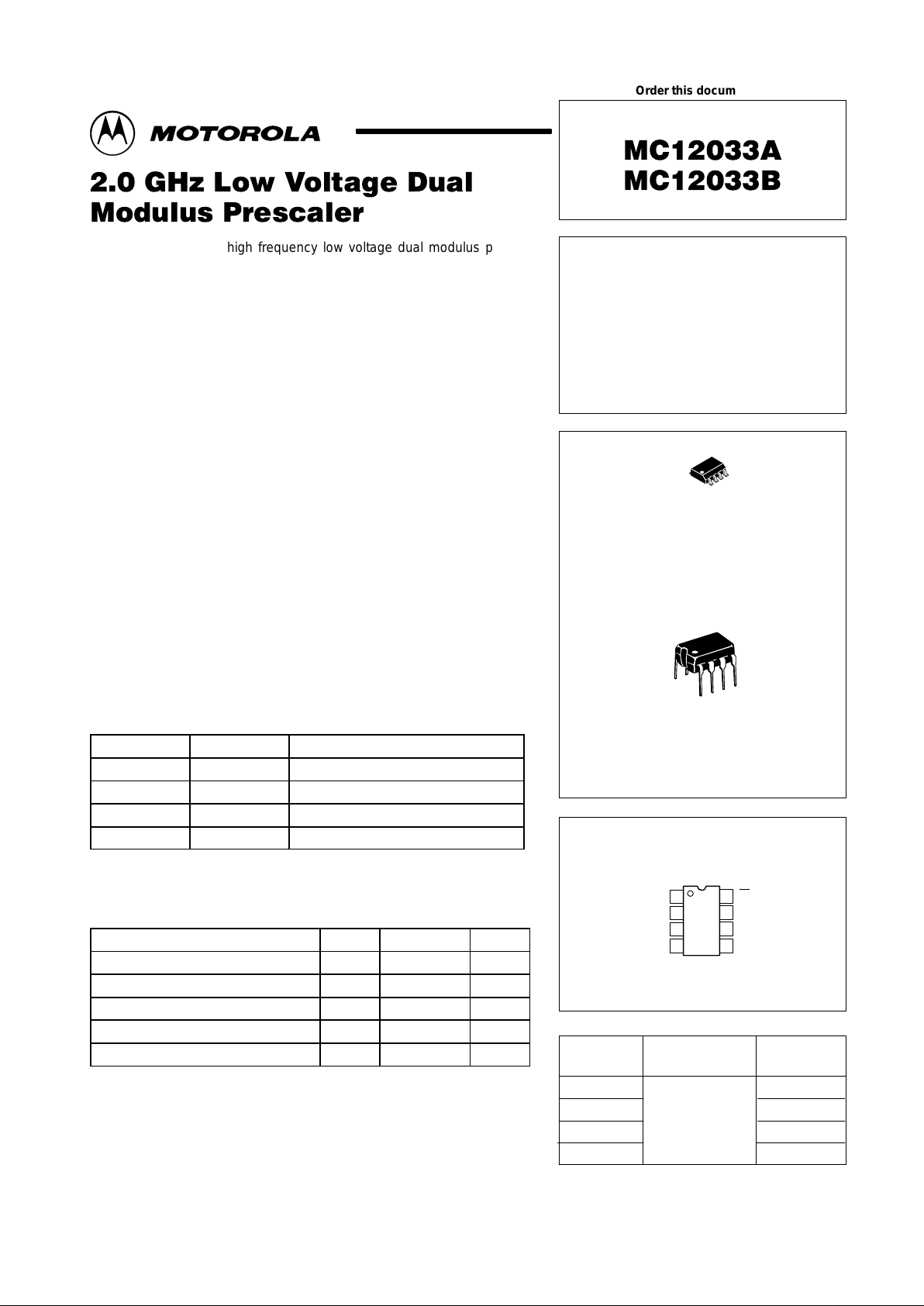
PIN CONNECTIONS
D SUFFIX
PLASTIC PACKAGE
CASE 751
(SO–8)
8
1
1
8
IN
(Top View)
8
IN
V
CC
SW
OUT
NC
MC
Gnd
7
6
5
1
2
3
4
Device
Operating
Temp Range
Package
ORDERING INFORMATION
MC12033AD
MC12033AP
TA = –40° to +85°C
SO–8
Plastic
MC12033BD
MC12033BP
SO–8
Plastic
The MC12033 is a high frequency low voltage dual modulus prescaler
used in phase–locked loop (PLL) applications. A high frequency input signal
up to 2.0 GHz is provided for cordless and cellular communication services
such as DECT, PHS, and PCS. The MC12033 can be operated down to a
minimum supply voltage of 2.7 V required for battery operated portable
systems.
The MC12033A can be used with CMOS synthesizer requiring positive
edges to trigger internal counters such as Motorola’s MC145XXX series in a
PLL to provide tuning signal up to 2.0 GHz in programmable frequency
steps. The MC12033B can be used with CMOS synthesizers requiring
negative edges to trigger internal counters.
A Divide Ratio Control (SW) permits selection of a 32/33 or 64/65 divide
ratio as desired.
The Modulus Control (MC) selects the proper divide number after SW has
been biased to select the desired divide ratio.
NOTE: The “B” Version Is Not Recommended for New Designs
• 2.0 GHz Toggle Frequency
• Supply Voltage 2.7 V to 5.0 Vdc
• Low Power 10.0 mA Typical at V
CC
= 2.7 V
• Operating Temperature Range of –40 to 85°C
• The MC12033 is Pin Compatible With the MC12022
• Short Setup Time (t
set
) 8ns Typical at 2.0 GHz
• Modulus Control Input Level Is Compatible
With Standard CMOS and TTL
FUNCTIONAL TABLE
SW MC Divide Ratio
H H 32
H L 33
L H 64
L L 65
NOTES: 1.SW: H = VCC, L = Open. A logic L can also be applied by grouunding this pin,
but this is not recommended due to increased power soncumption.
2.MC: H = 2.0 V to VCC, L = GND to 0.8 V.
MAXIMUM RATINGS
Parameter Symbol Value Unit
Power Supply Voltage, Pin 2 V
CC
–0.5 to 7.0 Vdc
Operating Temperature Range T
A
–40 to 85 °C
Storage Temperature Range Tstg –65 to 150 °C
Modulus Control Input, Pin 6 MC –0.5 to 6.5 Vdc
Maximum Output Current, Pin 4 I
O
10.0 mA
NOTE: ESD data available upon request.
Motorola, Inc. 1997 Rev 3
MC12033A MC12033B
2
MOTOROLA RF/IF DEVICE DATA
ELECTRICAL CHARACTERISTICS (VCC = 2.7 to 5.0 V; TA = –40 to 85°C, unless otherwise noted.)
Parameter Symbol Min Typ Max Unit
Toggle Frequency (Sine Wave) ft 0.5 2.4 2.0 GHz
Supply Current Output (Pin 2) VCC = 2.7 V
VCC = 5.0 V
I
CC
–
–
10.0
13.0
12.5
16.0
mA
Modulus Control Input HIGH (MC) V
IH1
2.0 – V
CC
V
Modulus Control Input LOW (MC) V
IL1
Gnd – 0.8 V
Divide Ratio Control Input HIGH (SW) V
IH2
V
CC
V
CC
V
CC
V
Divide Ratio Control Input LOW (SW) V
IL2
OPEN OPEN OPEN —
Output Voltage Swing (Note 1) CL = 8.0 pF; RL = 600 Ω V
OUT
0.8 1.2 – V
pp
Modulus Setup Time MC to OUT @ 2000 MHz t
set
– 8.0 10 ns
Input Voltage Sensitivity 500–2000 MHz V
IN
100 – 1000 mVpp
Output Current (Note 2) VCC = 2.7V , CL = 8.0 pF, RL = 600 Ω
VCC = 5.0 V, CL = 8.0 pF, RL = 1.5 kΩ
I
O
–
–
2.4
2.4
4.0
4.0
mA
NOTES: 1.Valid over voltage range 2.7 to 5.0 V; RL = 600 Ω @ VCC = 2.7 V; RL = 1.5 kΩ @ VCC = 5.0 V
2.Divide ratio of ÷32/33 @ 2.0 GHz
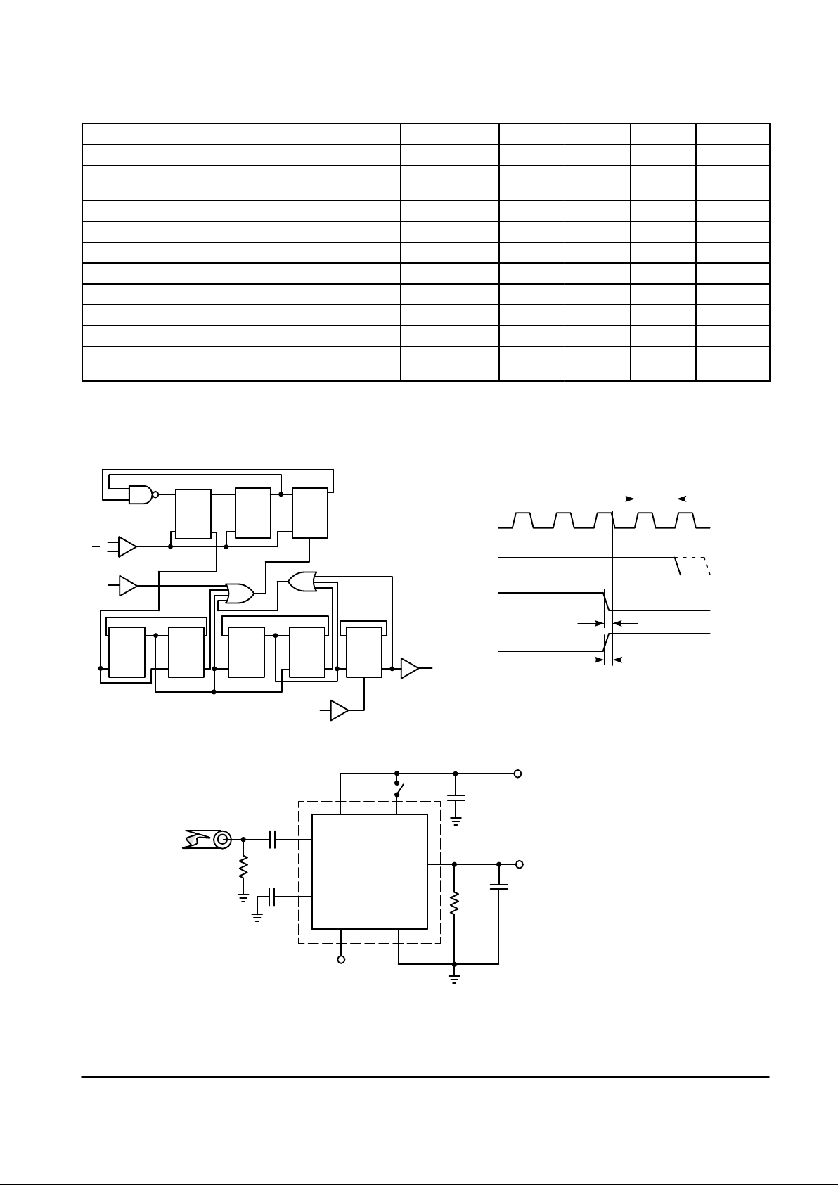
A
HGFED
In
MC
In
SW
Out
Q
S
Q
C
QBD
QC
QBD
QBC
QD
C
QBD
QBC
QD
QBC
QD
B
QBC
QD
C
QB
C
QD
M
Modulus setup time MC to out is the MC
setup or MC release plus the prop delay.
Prop. Delay
In
Out
MC
MC Setup
MC Release
Figure 1. Logic Diagram (MC12033A) Figure 2. Modulus Setup Time
Figure 3. AC Test Circuit
EXTERNAL COMPONENTS
C1 = C2 = 1000 pF
C3 = 0.1
µ
F
CL = 8.0 pF (Including Scope
and jig capacitance)
RL = 600
Ω
@ VCC = 2.7 V
RL = 1.5 k
Ω
@ VCC = 5.0 V
C
L
MC Input
C2
C1
C3
VCC = 2.7 to 5.0 V
50
Ω
Sine Wave Generator
SWV
CC
OUT
Gnd
MC
IN
IN
R
L
 Loading...