

Motorola MC12026AD, MC12026AP, MC12026BD, MC12026BP Datasheet
SEMICONDUCTOR TECHNICAL DATA
The MC12026 is a high frequency , low voltage dual modulus prescaler
used in phase–locked loop (PLL) applications.
The MC12026A can be used with CMOS synthesizers requiring
positive edges to trigger internal counters such as Motorola’s MC145xxx
series in a PLL to provide tuning signals up to 1.1GHz in programmable
frequency steps.
The MC12026B can be used with CMOS synthesizers requiring
negative edges to trigger internal counters.
A Divide Ratio Control (SW) permits selection of an 8/9 or 16/17 divide
ratio as desired.
The Modulus Control (MC) selects the proper divide number after SW
has been biased to select the desired divide ratio.
NOTE: The “B” Version Is Not Recommended for New Designs
• 1.1GHz Toggle Frequency
• Supply Voltage 4.5V to 5.5V
• Low Power 4.0mA Typical
• Operating Temperature Range of –40°C to +85°C
• The MC12026 is Pin Compatible With the MC12022
• Short Setup Time (t
• Modulus Control Input Level is Compatible With Standard CMOS
and TTL
) 6ns Typical @ 1.1GHz
set
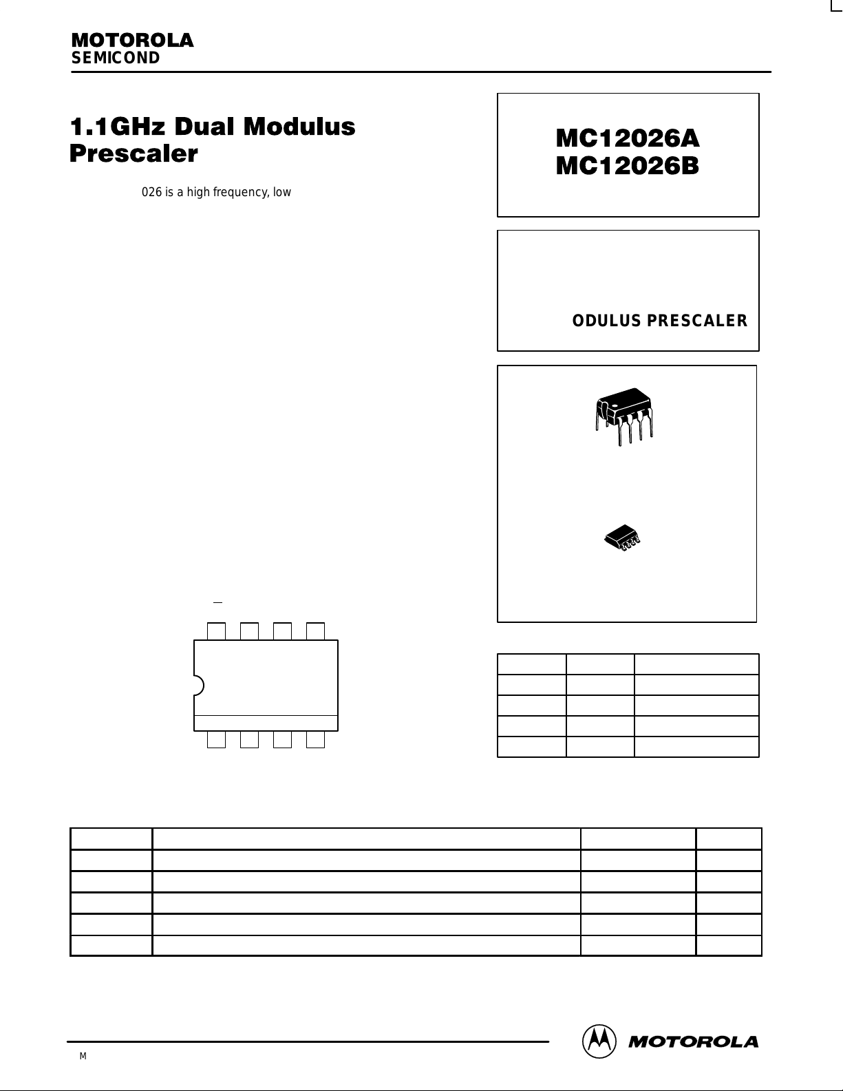
Pinout: 8–Lead Plastic (Top View)
IN
NC
MC
GND
8
7
6
5
1
2
3
4
V
SW
IN
CC
OUT
MECL PLL COMPONENTS
÷8/9, ÷16/17
DUAL MODULUS PRESCALER
8–LEAD PLASTIC PACKAGE
8–LEAD PLASTIC SOIC PACKAGE
SW MC Divide Ratio
H
H
L
L
Note: SW:H = VCC, L = OPEN
MC: H = 2.0V to VCC; L = GND to 0.8V
P SUFFIX
CASE 626–05
D SUFFIX
CASE 751–05
FUNCTION TABLE
H
L
H
L
8
9
16
17
MAXIMUM RATINGS
Symbol Characteristic Range Unit
V
CC
T
A
T
stg
MC Modulus Control Input, Pin 6 –0.5 to +6.5 Vdc
I
O
1/97
Motorola, Inc. 1997
Power Supply Voltage, Pin 2 –0.5 to +7.0 Vdc
Operating Temperature Range –40 to +85 °C
Storage Temperature Range –65 to +150 °C
Maximum Output Current, Pin 4 10.0 mA
1
REV 3
MC12026A MC12026B
ELECTRICAL CHARACTERISTICS (VCC = 4.5 to 5.5; TA = –40 to +85°C)
Symbol Characteristic Min Typ Max Unit
f
t
I
CC
V
IH1
V
IL1
V
IH2
V
IL2
V
out
t
SET
V
in
1. Divide Ratio of ÷8/9 at 1.1GHz, CL = 8pF
2. Divide Ratio of ÷16/17 at 1.1GHz, CL = 8pF
3. Assuming RL = 560Ω at 1.1GHz
Toggle Frequency (Sin Wave) 0.1 1.4 1.1 GHz
Supply Current Output Unloaded (Pin 2) — 4.0 5.3 mA
Modulus Control Input High (MC) 2.0 — V
Modulus Control Input Low (MC) GND — 0.8 V
Divide Ratio Control Input High (SW) VCC – 0.5V V
Divide Ratio Control Input Low (SW) OPEN OPEN OPEN —
Output Voltage Swing
(RL = 560Ω; IO = 5.5mA)
(RL = 1.1kΩ; IO = 2.9mA)
Modulus Setup Time MC to Out
Input Voltage Sensitivity
100–250MHz
250–1 100MHz
1
2
3
1.0 1.6 — V
— 6 9 ns
400
100
CC
—
—
CC
VCC + 0.5V V
1000
1000
V
p–p
mVpp
In
In
MC
SW
DQ
CQB
1
0
DQ
CQB
DCQB
Q
DQ
C
M
DCQB
Q
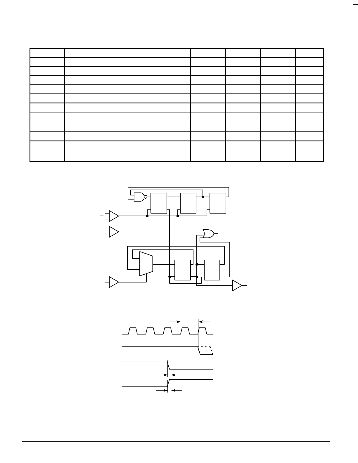
Figure 1. Logic Diagram (MC12026A)
Prop. Delay
In
Out
QB
Out
MC Setup
MC Release
Modulus setup time MC to out is the MC
setup or MC release plus the prop delay.
MC
Figure 2. Modulus Setup Time
MOTOROLA HIPERCOMM
2
BR1334 — Rev 4
 Loading...