

Motorola MC12022LVAD, MC12022LVAP, MC12022LVBD, MC12022LVBP Datasheet
SEMICONDUCTOR
TECHNICAL DATA
MECL PLL COMPONENTS
÷64/65, ÷128/129
DUAL MODULUS PRESCALER
Order this document by MC12022LVA/D
P SUFFIX
PLASTIC PACKAGE
CASE 626
D SUFFIX
PLASTIC PACKAGE
CASE 751
(SO–8)
8
1
1
8
Device
Operating
Temp Range
Package
ORDERING INFORMATION
MC12022LVAD
MC12022LVAP
TA =
–40° to +85°C
SO–8
Plastic
PIN CONNECTIONS
IN
(Top View)
8
IN
V
CC
SW
OUT
NC
MC
Gnd
7
6
5
1
2
3
4
MC12022LVBD
MC12022LVBP
SO–8
Plastic
The MC12022LVA can be used with CMOS synthesizers requiring
positive edges to trigger internal counters such as Motorola’s MC145XXX
series in a PLL to provide tuning signals up to 1.1 GHz in programmable
frequency steps.
The MC12022LVB can be used with CMOS synthesizers requiring
negative edges to trigger internal counters.
A Divide Ratio Control (SW) permits selection of a 64/65 or 128/129 divide
ratio as desired.
The Modulus Control (MC) selects the proper divide number after SW has
been biased to select the desired divide ratio.
NOTE: The “B” Version Is Not Recommended for New Designs
• 1.1 GHz Toggle Frequency
• Supply Voltage of 2.7 to 5.0 V
• Low–Power 4.0 mA Typical at V
CC
= 2.7 V
• Operating Temperature Range of –40 to 85°C
• Short Setup Time (t
set
) 16ns Maximum @ 1.1 GHz
• Modulus Control Input Level Is Compatible With Standard CMOS
and TTL
FUNCTIONAL TABLE
SW MC Divide Ratio
H H 64
H L 65
L H 128
L L 129
NOTES: 1.SW: H = VCC, L = Open. A logic L can also be applied by grouunding this pin,
but this is not recommended due to increased power soncumption.
2.MC: H = 2.0 V to VCC, L = GND to 0.8 V.
DESIGN GUIDE
Criteria Value Unit
Internal Gate Count* 67 ea
Internal Gate Propagation Delay 200 ps
Internal Gate Power Dissipation 0.75 mW
Speed Power Product 0.15 pJ
NOTE: * Equivalent to a two–input NAND gate
Motorola, Inc. 1997 Rev 3
MC12022LVA MC12022LVB
2
MOTOROLA RF/IF DEVICE DATA
MAXIMUM RATINGS
Rating Symbol Value Unit
Power Supply Voltage, Pin 2 V
CC
–0.5 to 7.0 Vdc
Operating Temperature Range T
A
–40 to 85 °C
Storage Temperature Range T
stg
–65 to 150 °C
Modulus Control Input, Pin 6 MC –0.5 to 6.5 Vdc
NOTE; ESD data available upon request.
ELECTRICAL CHARACTERISTICS (V
CC
= 4.5 to 5.5 V; TA = –40°C to 85°C, unless otherwise noted.)
Characteristic
Symbol Min Typ Max Unit
Toggle Frequency (Sine Wave Input) f
t
0.1 1.4 1.1 GHz
Supply Current Output Unloaded (Pin 2) I
CC
– 4.7 6.5 mA
Supply Current Output Unloaded (Pin 2) at 5.0 Vdc I
CCH
5.8 8.0 mA
Modulus Control Input High (MC) V
IH1
2.0 – V
CC
V
Modulus Control Input Low (MC) V
IL1
– – 0.8 V
Divide Ratio Control Input High (SW) V
IH2
V
CC
V
CC
V
CC
Vdc
Divide Ratio Control Input Low (SW) V
IL2
Open Open Open –
Output Voltage Swing (CL = 12 pF; RL = 1.1 kΩ at 2.7 Vdc) V
out
0.8 1.0 – V
pp
Output Voltage Swing (CL = 12 pF; RL = 2.2 kΩ at 5.0 Vdc) V
out
1.0 1.6 – V
pp
Modulus Setup Time MC to Out t
set
– 11 16 ns
Input Voltage Sensitivity 250–1100 MHz
100–250 MHz
V
in(min)
100
400
–
–
1500
1500
mVpp
Output Current (CL = 12 pF; RL = 2.2 kΩ at 2.7 Vdc) I
O
– 1.2 4.0 mA
Output Current (CL = 12 pF; RL = 2.2 kΩ at 5.0 Vdc) I
O
– 1.2 4.0 mA
MC12022LVA MC12022LVB
3
MOTOROLA RF/IF DEVICE DATA
A
HGFED
In
MC
In
SW
Out
Q
S
Q
C
QBD
QC
QBD
QBC
QD
C
QBD
QBC
QD
QBC
QD
B
QBC
QD
C
QB
C
QD
M
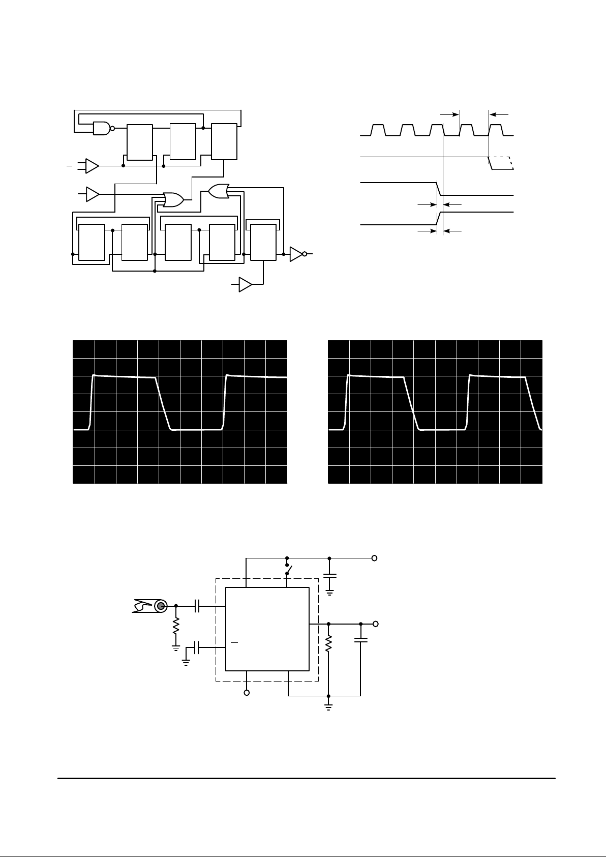
Modulus setup time MC to out is the MC
setup or MC release plus the prop delay.
Prop. Delay
In
Out
MC
MC Setup
MC Release
Figure 1. Logic Diagram (MC12022LVA) Figure 2. Modulus Setup Time
Figure 3. Typical Output Waveforms
(÷128, 1.1GHz Input Frequency, VCC = 5.0V, TA = 25°C, Output Loaded)(÷64, 500MHz Input Frequency, VCC = 5.0V, TA = 25°C, Output Loaded)
500 m
20 ns
≈
500 m
20 ns
≈
Figure 4. AC Test Circuit
EXTERNAL COMPONENTS
C1 = C2 = 1000pF
C3 = 0.1
µ
F
CL = 12pF (Including Scope
and jig capacitance)
RL = 2.2k
Ω
(at +5.0Vdc)
RL = 1.1k
Ω
(at +2.7Vdc)
C
L
MC Input
C2
C1
C3
VCC = 2.7 to 5.0Vdc
50
Ω
Sine Wave Generator
SWV
CC
OUT
GND
MC
IN
IN
R
L
 Loading...