

MOTOROLA MC10H350FNR2, MC10H350L, MC10H350M, MC10H350MEL, MC10H350ML1 Datasheet
...
SEMICONDUCTOR TECHNICAL DATA
2–57
REV 6
Motorola, Inc. 1996
9/96
" !# #
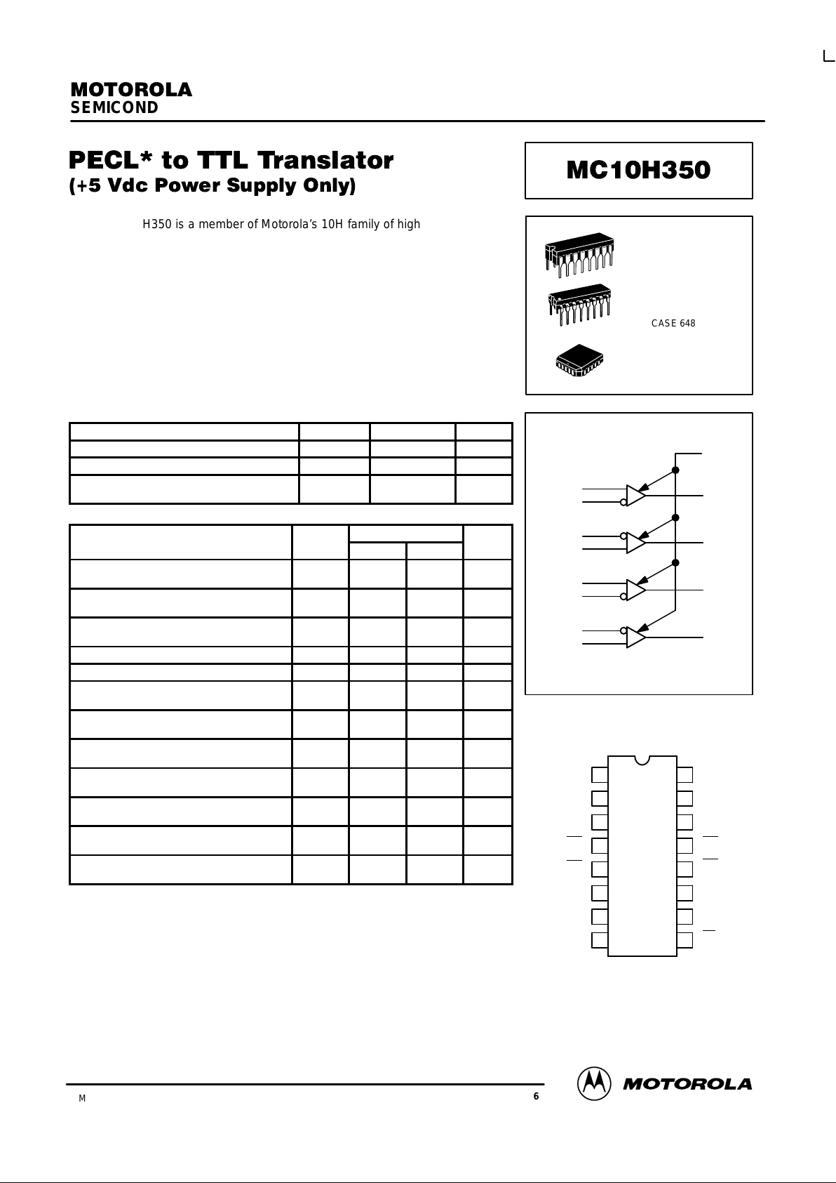
The MC10H350 is a member of Motorola’s 10H family of high performance
ECL logic. It consists of 4 translators with differential inputs and TTL outputs.
The 3–state outputs can be disabled by applying a HIGH TTL logic level on the
common OE input.
The MC10H350 is designed to be used primarily in systems incorporating
both ECL and TTL logic operating off a common power supply. The separate
VCC power pins are not connected internally and thus isolate the noisy TTL V
CC
runs from the relatively quiet ECL VCC runs on the printed circuit board. The
differential inputs allow the H350 to be used as an inverting or noninverting
translator, or a dif ferential line receiver . The H350 can also drive CMOS with the
addition of a pullup resistor.
• Propagation Delay, 3.5 ns Typical • MECL 10K–Compatible
MAXIMUM RATINGS
Characteristic Symbol Rating Unit
Power Supply (VEE = Gnd) V
CC
7.0 Vdc
Operating T emperature Range T
A
0 to +75 °C
Storage T emperature Range — Plastic
— Ceramic
T
stg
–55 to +150
–55 to +165
°C
°C
ELECTRICAL CHARACTERISTICS (VCC = 5.0 V ±5%) (See Note 1)
TA = 0°C to 75°C
Characteristic Symbol Min Max Unit
Power Supply Current TTL
ECL
I
CC
—
—
20
12
mA
Input Current High Pin 9
Others
I
IH
I
INH
—
—
20
50
µA
Input Current Low Pin 9
Others
I
IL
I
INL
—
—
–0.6
50
mA
µA
Input Voltage High Pin 9 V
IH
2.0 — Vdc
Input Voltage Low Pin 9 V
IL
— 0.8 Vdc
Differential Input Voltage (1)
Pins 3–6, 11–14 (1)
V
DIFF
350 — mV
Voltage Common Mode
Pins 3–6, 11–14
V
CM
2.8 V
CC
Vdc
Output Voltage High
IOH = 3.0 mA
V
OH
2.7 — Vdc
Output Voltage Low
IOL = 20 mA
V
OL
— 0.5 Vdc
Short Circuit Current
V
OUT
= 0 V
I
OS
–60 –150 mA
Output Disable Current High
V
OUT
= 2.7 V
I
OZH
— 50 µA
Output Disable Current Low
V
OUT
= 0.5 V
I
OZL
— –50 µA
(1) Common mode input voltage to pins 3–4, 5–6, 1 1–12, 13–14 must be between the values of 2.8
V and 5.0 V. This common mode input voltage range includes the differential input swing.
(2) For single ended use, apply 3.75 V (VBB) to either input depending on output polarity required.
Signal level range to other input is 3.3 V to 4.2 V.
(3) Any unused gates should have the inverting inputs tied to VCC and the non–inverting inputs tied
to ground to prevent output glitching.
(4) 1.0 V to 2.0 V w/50 pF into 500 ohms.
*Positive Emitter Coupled Logic
LOGIC DIAGRAM
DIP
PIN ASSIGNMENT
ECL V
CC
A
OUT
A
IN
A
IN
B
IN
B
IN
B
OUT
GND
TTL V
CC
C
OUT
C
IN
C
IN
D
IN
D
IN
D
OUT
OE
16
15
14
13
12
11
10
9
1
2
3
4
5
6
7
8
VCC (+5.0 VDC) = PINS 1 AND 16
GND = PIN 8
15
14
13
10
12
11
7
6
5
2
4
3
9
L SUFFIX
CERAMIC PACKAGE
CASE 620–10
P SUFFIX
PLASTIC PACKAGE
CASE 648–08
FN SUFFIX
PLCC
CASE 775–02
Pin assignment is for Dual–in–Line Package.
For PLCC pin assignment, see the Pin Conversion
T ables on page 6–11 of the Motorola MECL Data
Book (DL122/D).
MC10H350
MOTOROLA MECL Data
DL122 — Rev 6
2–58
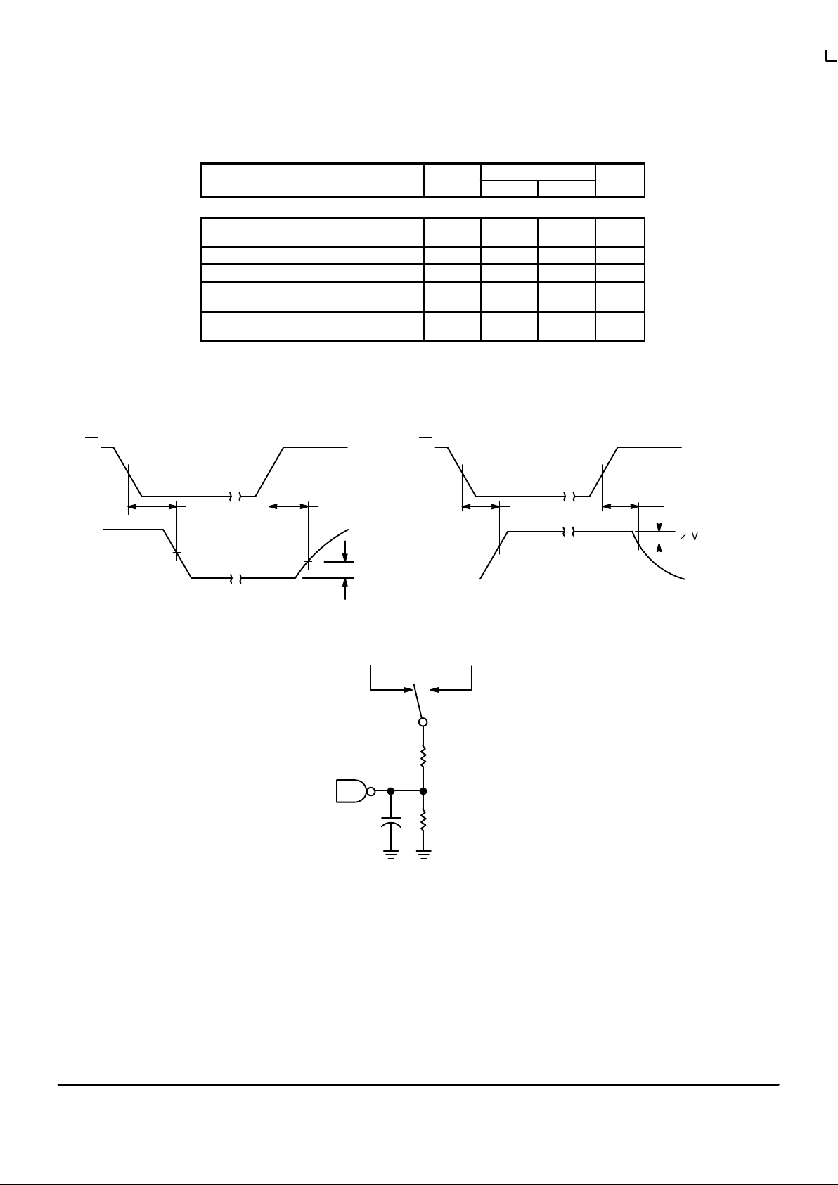
ELECTRICAL CHARACTERISTICS (VCC = 5.0 V ±5%) (See Notes 1 & 4)
TA = 0°C to 75°C
Characteristic Symbol Min Max Unit
AC PARAMETERS (CL = 50 pF) (VCC = 5.0 ± 5%) (TA = 0°C to 75°C)
Propagation Delay
Data
t
pd
1.5 5.0 ns
Rise Time t
r
0.3 1.6 ns
Fall Time t
f
0.3 1.6 ns
Output Disable Time t
pdLZ
t
pdHZ
2.0
2.0
6.0
6.0
ns
Output Enable Time t
pdZL
t
pdZH
2.0
2.0
8.0
8.0
ns
T
PZL
0.3 V
OE
1.5 V1.5 V
1.5 V
T
PZH
T
PHZ
3–STATE OUTPUT HIGH ENABLE AND
DISABLE TIMES
OE
V
OUT
0.3 V
V
OL
1.5 V1.5 V
1.5 V
T
PLZ
Q
VOH≈ 3.5 V
+7.0 V OPEN
ALL OTHERT
PZL
, T
PLZ
, O, C,
500
Ω
500
Ω
D.U.T
.
50 PF
3–STATE SWITCHING WAVEFORMS
3–STATE OUTPUT LOW ENABLE AND
DISABLE TIMES
TEST LOAD
*INCLUDES JIG AND PROBE CAPACITANCE
V
OUT
Application Note: Pin 9 is an OE and the 10H350 is disabled when OE is at VIH or higher.
 Loading...