

Motorola MC10H334L, MC10H334P, MC10H334FN Datasheet
SEMICONDUCTOR TECHNICAL DATA
2–37
REV 5
Motorola, Inc. 1996
3/93
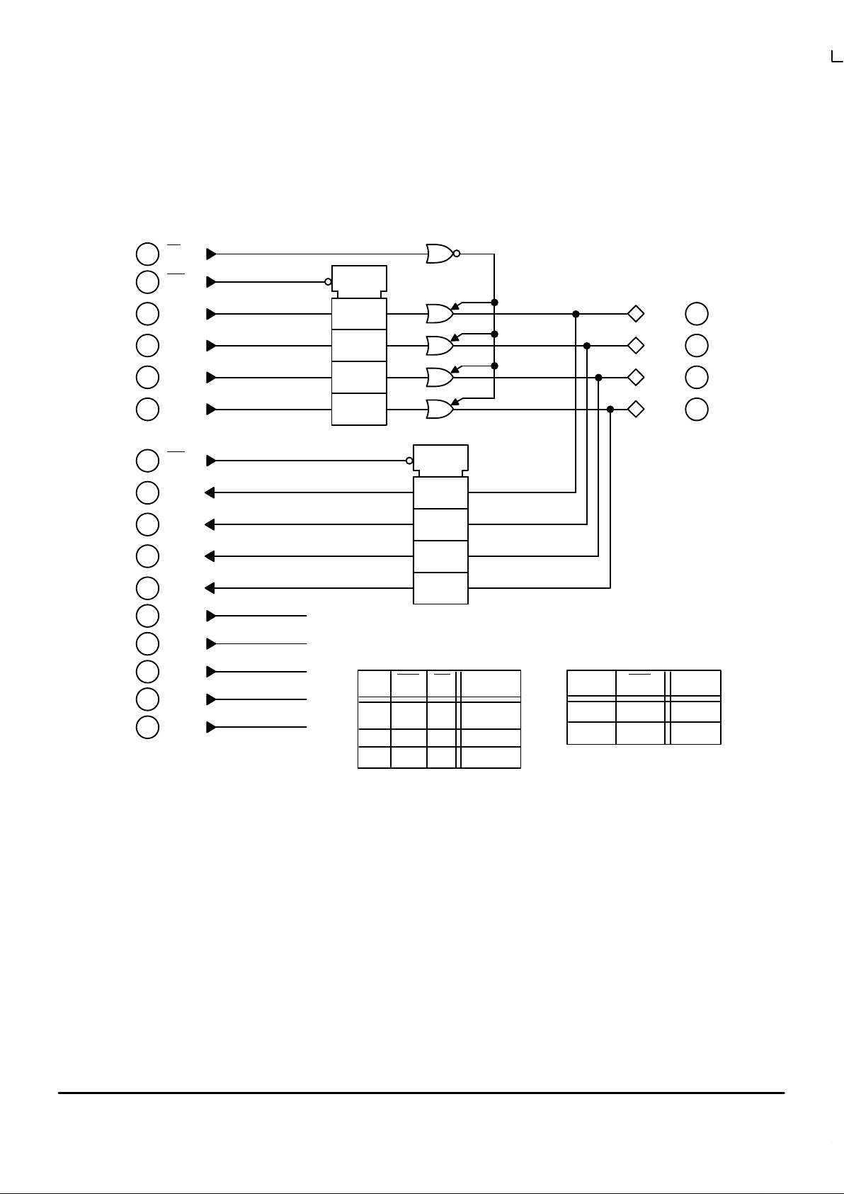
The MC10H334 is a Quad Bus Driver/Receiver with transmit and receiver
latches. When disabled, (OE
= high) the bus outputs will fall to –2.0 V . Data to
be transmitted or received is passed through its respective latch when the
respective latch enable (DLE
and RLE) is at a low level. Information is latched
on the positive transition of DLE
and RLE. The parameters specified are with
25 Ω loading on the bus drivers and 50 Ω loads on the receivers.
• Propagation Delay, 1.6 ns Typical Data–to–Output
• Improved Noise Margin 150 mV (Over Operating Voltage and
Temperature Range)
• Voltage Compensated
• MECL 10K–Compatible
MAXIMUM RATINGS
Characteristic Symbol Rating Unit
Power Supply (VCC = 0) V
EE
–8.0 to 0 Vdc
Input Voltage (VCC = 0) V
I
0 to V
EE
Vdc
Output Current— Continuous
— Surge
I
out
50
100
mA
Operating Temperature Range T
A
0 to +75 °C
Storage Temperature Range— Plastic
— Ceramic
T
stg
–55 to +150
–55 to +165
°C
°C
ELECTRICAL CHARACTERISTICS (VEE = –5.2 V ±5%) (See Note)
0° 25° 75°
Characteristic Symbol Min Max Min Max Min Max Unit
Power Supply Current I
E
— 161 — 161 — 161 mA
Input Current High
Pins 5,6,15,16
Pins 7,14
Pin 17
I
inH
—
—
—
397
460
520
—
—
—
273
297
357
—
—
—
273
297
357
µA
Input Current Low I
inL
0.5 — 0.5 — 0.3 — µA
High Output Voltage V
OH
–1.02 –0.84 –0.98 –0.81 –0.92 –0.735 Vdc
Low Output Voltage V
OL
–1.95 –1.63 –1.95 –1.63 –1.95 –1.60 Vdc
High Input Voltage V
IH
–1.17 –0.84 –1.13 –0.81 –1.07 –0.735 Vdc
Low Input Voltage V
IL
–1.95 –1.48 –1.95 –1.48 –1.95 –1.45 Vdc
AC PARAMETERS
Propagation Delay
Data–to–Bus Output
DLE
–to–Bus Output
OE
–to–Bus Output
Bus–to–R0
RLE
–to–R0
Data–to–Receiver
R0
t
pd
0.5
1.0
0.5
0.5
0.5
1.0
2.5
2.7
2.5
1.9
2.1
3.8
0.5
1.0
0.5
0.5
0.5
1.0
2.5
2.7
2.5
1.9
2.1
3.8
0.5
1.0
0.5
0.5
0.5
1.0
2.5
2.7
2.5
1.9
2.1
3.8
ns
Rise Time t
r
0.5 2.2 0.5 2.2 0.5 2.2 ns
Fall Time t
f
0.5 2.2 0.5 2.2 0.5 2.2 ns
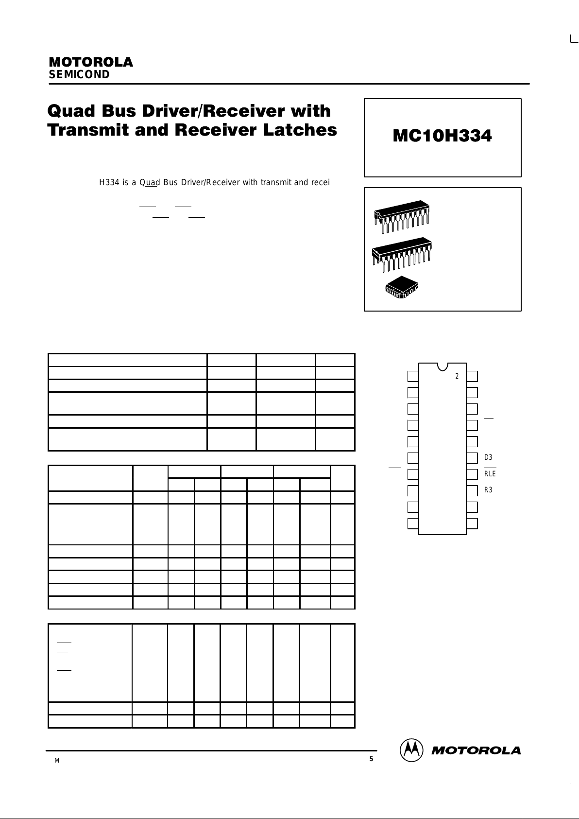
DIP & PLCC
PIN ASSIGNMENT
V
CC
BUS1
BUS0
VCC02
D1
D0
DLE
R0
V
CC03
BUS2
BUS3
OE
D2
D3
RLE
R3
20
19
18
17
16
15
14
13
1
2
3
4
5
6
7
8
R1
V
EE
R2
V
CC02
12
11
9
10
NOTE:
Each MECL 10H series circuit has been designed
to meet the dc specifications shown in the test table,
after thermal equilibrium has been established. The
circuit is in a test socket or mounted on a printed
circuit board and transverse air flow greater than
500 Ifpm is maintained. Receiver outputs are
terminated through a 50–ohm resistor to –2.0 volts
dc. Bus outputs are terminated through a 25–ohm
resistor to –2.0 volts dc.
Pin assignment is for Dual–in–Line Package.
For PLCC pin assignment, see the Pin Conversion
T ables on page 6–11 of the Motorola MECL Data
Book (DL122/D).
L SUFFIX
CERAMIC PACKAGE
CASE 732–03
P SUFFIX
PLASTIC PACKAGE
CASE 738–03
FN SUFFIX
PLCC
CASE 775–02
MC10H334
MOTOROLA MECL Data
DL122 — Rev 6
2–38
OE
QD
RECEIVER TRUTH TABLEDRIVER TRUTH TABLE
D DLE Bus
n+1
BUS0
BUS1
BUS2
BUS3
V
CC02
D1
D0
DLE
R0
R1
V
EE
OE
D2
D3
RLE
R3
R2
V
CC03
V
CC
V
CC01
QD
OUTPUT
LATCH
RECEIVER
LATCH
7
6
5
16
15
8
14
9
12
13
10
1
4
11
20
3
2
19
18
QD
QD
G
DQ
DQ
DQ
DQ
G
LOGIC DIAGRAM
17
X X H –2.0 V
DL L D
X H L Bus
n
Bus RLE R
n+1
Bus
X
L
H
Bus
R
n
 Loading...