

MOTOROLA MC10H334FNR2 Datasheet
SEMICONDUCTOR TECHNICAL DATA
The MC10H334 is a Quad Bus Driver/Receiver with transmit and receiver
latches. When disabled, (OE
be transmitted or received is passed through its respective latch when the
respective latch enable (DLE
on the positive transition of DLE
25 Ω loading on the bus drivers and 50 Ω loads on the receivers.
• Propagation Delay, 1.6 ns Typical Data–to–Output
• Improved Noise Margin 150 mV (Over Operating Voltage and
Temperature Range)
• Voltage Compensated
• MECL 10K–Compatible
MAXIMUM RATINGS
Characteristic Symbol Rating Unit
Power Supply (VCC = 0) V
Input Voltage (VCC = 0) V
Output Current— Continuous
Operating Temperature Range T
Storage Temperature Range— Plastic
— Surge
ELECTRICAL CHARACTERISTICS (VEE = –5.2 V ±5%) (See Note)
Characteristic Symbol Min Max Min Max Min Max Unit
Power Supply Current I
Input Current High
Pins 5,6,15,16
Pins 7,14
Pin 17
Input Current Low I
High Output Voltage V
Low Output Voltage V
High Input Voltage V
Low Input Voltage V
AC PARAMETERS
Propagation Delay
Data–to–Bus Output
DLE
–to–Bus Output
OE
–to–Bus Output
Bus–to–R0
RLE
–to–R0
Data–to–Receiver
R0
Rise Time t
Fall Time t
= high) the bus outputs will fall to –2.0 V. Data to
and RLE) is at a low level. Information is latched
and RLE. The parameters specified are with
EE
I
I
out
A
T
397
460
520
2.5
2.7
2.5
1.9
2.1
3.8
stg
—
—
—
0.5
1.0
0.5
0.5
0.5
1.0
— Ceramic
0° 25° 75°
— 161 — 161 — 161 mA
—
—
—
0.5 — 0.5 — 0.3 — µA
–1.02 –0.84 –0.98 –0.81 –0.92 –0.735 Vdc
–1.95 –1.63 –1.95 –1.63 –1.95 –1.60 Vdc
–1.17 –0.84 –1.13 –0.81 –1.07 –0.735 Vdc
–1.95 –1.48 –1.95 –1.48 –1.95 –1.45 Vdc
IL
0.5
1.0
0.5
0.5
0.5
1.0
0.5 2.2 0.5 2.2 0.5 2.2 ns
r
0.5 2.2 0.5 2.2 0.5 2.2 ns
f
I
t
E
inH
inL
OH
OL
IH
pd
–8.0 to 0 Vdc
0 to V
EE
50
100
0 to +75 °C
–55 to +150
–55 to +165
273
297
357
2.5
2.7
2.5
1.9
2.1
3.8
—
—
—
0.5
1.0
0.5
0.5
0.5
1.0
Vdc
mA
°C
°C
273
297
357
2.5
2.7
2.5
1.9
2.1
3.8
µA
ns
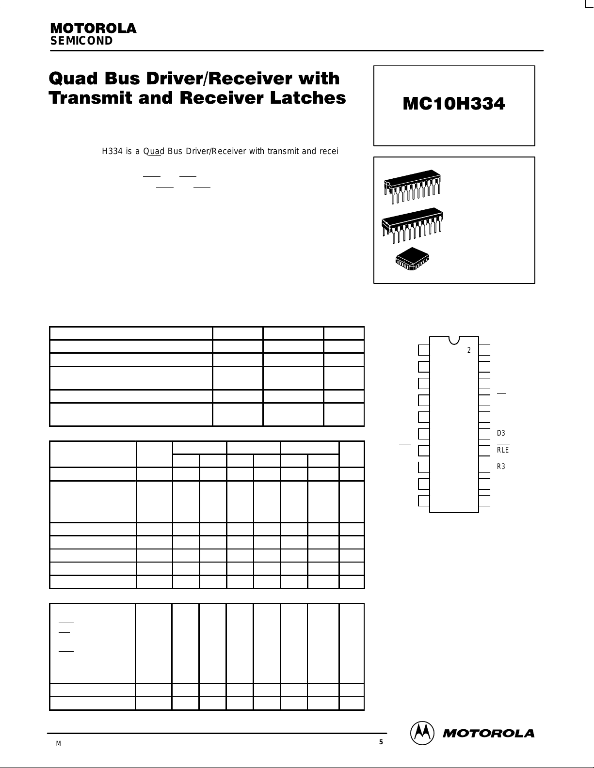
L SUFFIX
CERAMIC PACKAGE
CASE 732–03
P SUFFIX
PLASTIC PACKAGE
CASE 738–03
FN SUFFIX
PLCC
CASE 775–02
DIP & PLCC
PIN ASSIGNMENT
V
CC
BUS1
BUS0
VCC02
D1
D0
DLE
R0
R1
V
EE
Pin assignment is for Dual–in–Line Package.
For PLCC pin assignment, see the Pin Conversion
T ables on page 6–11 of the Motorola MECL Data
NOTE:
Each MECL 10H series circuit has been designed
to meet the dc specifications shown in the test table,
after thermal equilibrium has been established. The
circuit is in a test socket or mounted on a printed
circuit board and transverse air flow greater than
500 Ifpm is maintained. Receiver outputs are
terminated through a 50–ohm resistor to –2.0 volts
dc. Bus outputs are terminated through a 25–ohm
resistor to –2.0 volts dc.
1
2
3
4
5
6
7
8
9
10
Book (DL122/D).
20
19
18
17
16
15
14
13
12
11
V
CC03
BUS2
BUS3
OE
D2
D3
RLE
R3
R2
V
CC02
3/93
Motorola, Inc. 1996
2–37
REV 5
MC10H334
17
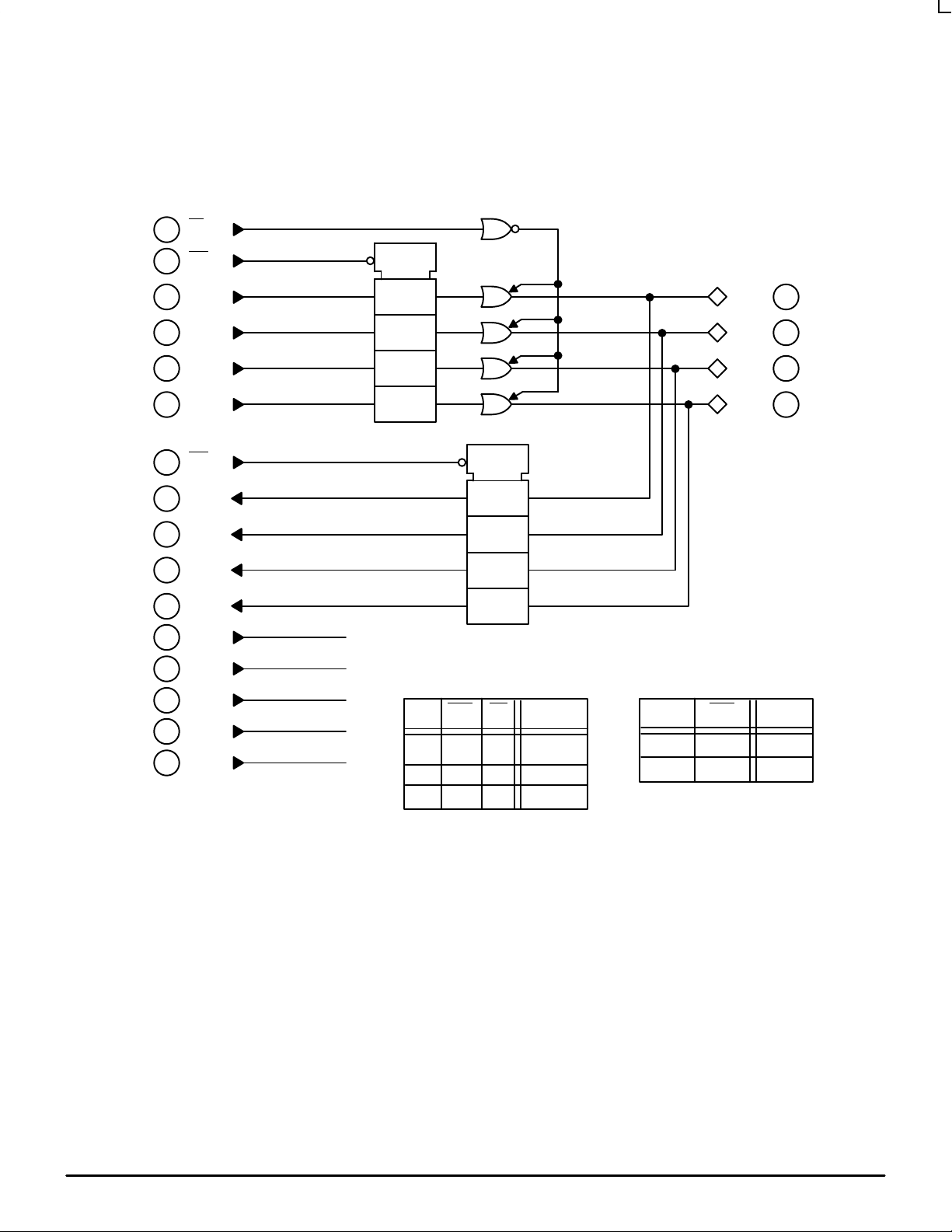
LOGIC DIAGRAM
OE
16
15
14
12
13
10
11
20
7
DLE
D0
6
D1
5
D2
D3
RLE
8
R0
R1
9
R2
R3
V
EE
1
V
CC
V
4
CC01
V
CC02
V
CC03
G
DQ
DQ
DQ
DQ
OUTPUT
LATCH
D DLE Bus
X X H –2.0 V
DL L D
X H L Bus
G
QD
QD
QD
QD
RECEIVER
LATCH
OE
n+1
n
BUS0
BUS1
BUS2
BUS3
RECEIVER TRUTH TABLEDRIVER TRUTH TABLE
Bus RLE R
Bus
X
L
H
19
18
n+1
Bus
R
3
2
n
MOTOROLA MECL Data
2–38
DL122 — Rev 6
 Loading...