

Motorola MC10H332L, MC10H332P Datasheet
SEMICONDUCTOR TECHNICAL DATA
2–13
REV 5
Motorola, Inc. 1996
3/93
!
The MC10H332 is a Dual Bus Driver/Receiver with four–to–one output
multiplexers. These multiplexers have common selects and output enable.
When disabled, (OE
= high) the bus outputs go to –2.0 V. The parameters
specified are with 25 Ω loading on the bus drivers and 50 Ω loads on the
receivers.
• Propagation Delay, 1.5 ns Typical Data–to–Output
• Improved Noise Margin 150 mV (Over Operating Voltage and
Temperature Range)
• Voltage Compensated
• MECL 10K–Compatible
MAXIMUM RATINGS
Characteristic Symbol Rating Unit
Power Supply (VCC = 0) V
EE
–8.0 to 0 Vdc
Input Voltage (VCC = 0) V
I
0 to V
EE
Vdc
Output Current— Continuous
— Surge
I
out
50
100
mA
Operating Temperature Range T
A
0 to +75 °C
Storage Temperature Range— Plastic
— Ceramic
T
stg
–55 to +150
–55 to +165
°C
°C
ELECTRICAL CHARACTERISTICS (VEE = –5.2 V ±5%) (See Note)
0° 25° 75°
Characteristic Symbol Min Max Min Max Min Max Unit
Power Supply Current I
E
— 115 — 110 — 115 mA
Input Current High
Pins 3,4,5,6,14,
15,16,17
Pins 7,8
Pins 13, 18
I
inH
—
—
—
667
437
456
—
—
—
417
273
285
—
—
—
417
273
285
µA
Input Current Low I
inL
0.5 — 0.5 — 0.3 — µA
High Output Voltage V
OH
–1.02 –0.84 –0.98 –0.81 –0.92 –0.735 Vdc
Low Output Voltage V
OL
–1.95 –1.63 –1.95 –1.63 –1.95 –1.60 Vdc
High Input Voltage V
IH
–1.17 –0.84 –1.13 –0.81 –1.07 –0.735 Vdc
Low Input Voltage V
IL
–1.95 –1.48 –1.95 –1.48 –1.95 –1.45 Vdc
AC PARAMETERS
Propagation Delay
Data–to–Bus Output
Select–to–Bus
Output
OE
–to–Bus Output
Bus–to–Receiver
Select–to–Receiver
RE
–to–Receiver
Data–to–Receiver
t
pd
0.8
0.8
0.8
0.8
1.8
0.8
1.3
3.0
3.4
2.4
2.1
4.5
2.2
4.0
0.8
0.8
0.8
0.8
1.8
0.8
1.3
3.0
3.4
2.4
2.1
4.5
2.2
4.0
0.8
0.8
0.8
0.8
1.8
0.8
1.3
3.2
3.8
2.6
2.4
5.0
2.5
4.5
ns
Rise Time t
r
0.5 2.0 0.5 2.0 0.5 2.1 ns
Fall Time t
f
0.5 2.0 0.5 2.0 0.5 2.1 ns
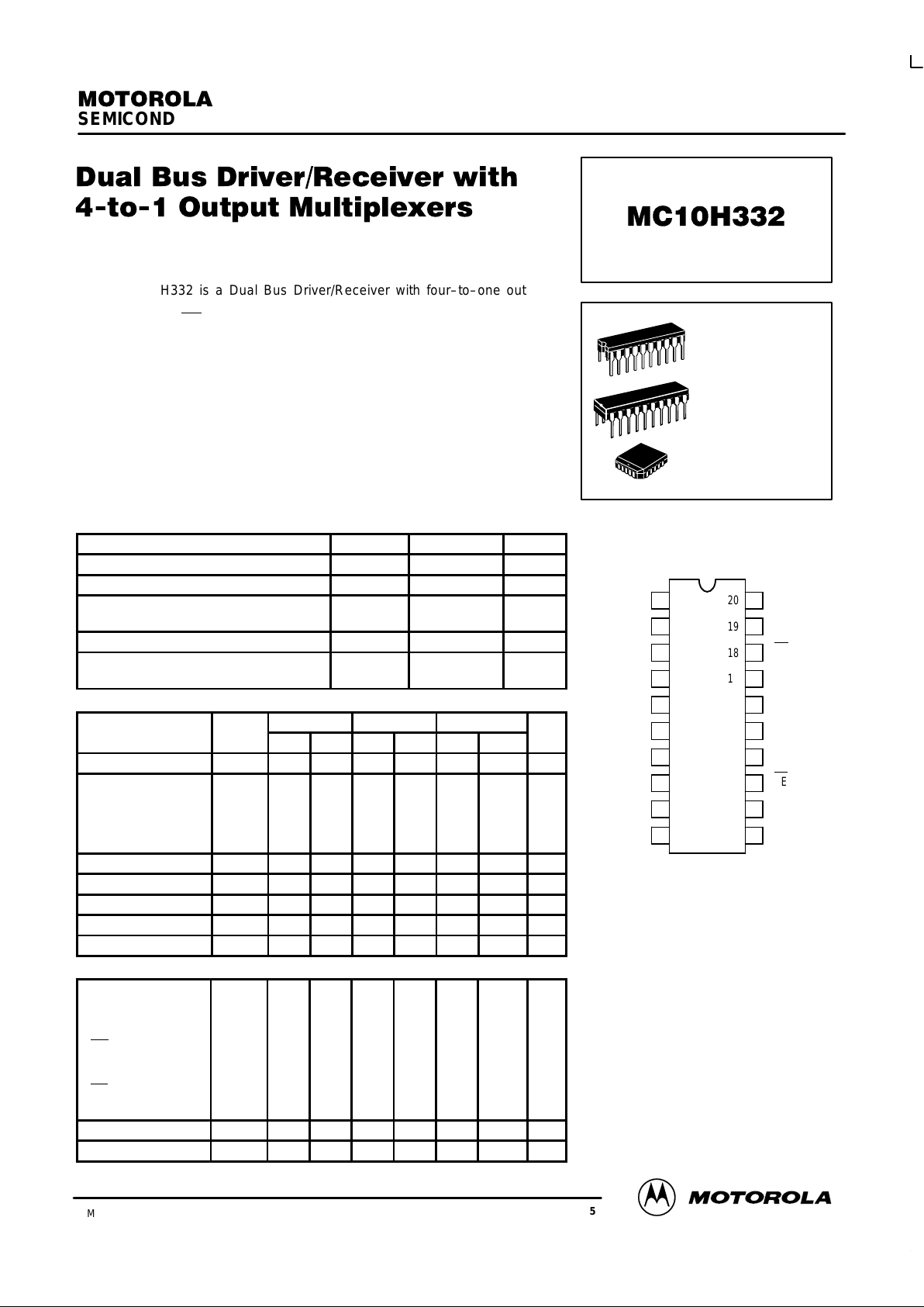
DIP & PLCC
PIN ASSIGNMENT
V
CC
X
BUS
X0
X1
X2
X3
S0
S1
V
CC02
Y
BUS
OE
Y0
Y1
Y2
Y3
RE
20
19
18
17
16
15
14
13
1
2
3
4
5
6
7
8
X
IN
V
EE
Y
IN
V
CC01
12
11
9
10
NOTE:
Each MECL 10H series circuit has been designed
to meet the dc specifications shown in the test table,
after thermal equilibrium has been established. The
circuit is in a test socket or mounted on a printed
circuit board and transverse air flow greater than
500 Ifpm is maintained. Receiver outputs are
terminated through a 50–ohm resistor to –2.0 volts
dc. Bus outputs are terminated through a 25–ohm
resistor to –2.0 volts dc.
L SUFFIX
CERAMIC PACKAGE
CASE 732–03
P SUFFIX
PLASTIC PACKAGE
CASE 738–03
FN SUFFIX
PLCC
CASE 775–02
Pin assignment is for Dual–in–Line Package.
For PLCC pin assignment, see the Pin Conversion
T ables on page 6–11 of the Motorola MECL Data
Book (DL122/D).
MC10H332
MOTOROLA MECL Data
DL122 — Rev 6
2–14
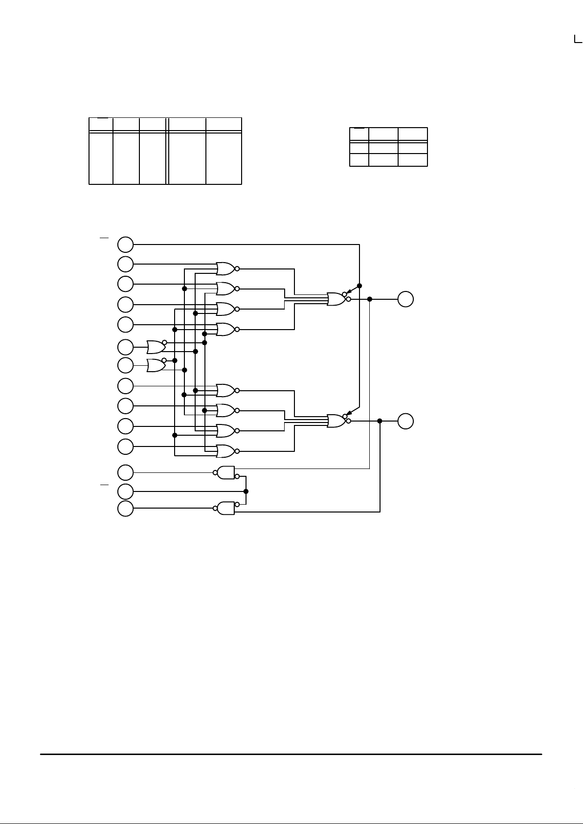
MULTIPLEXER TRUTH TABLE RECEIVER TRUTH
TABLE
V
CC
= PIN 1
V
CC01
= PIN 11
V
CC02
= PIN 20
V
EE
= PIN 10
OE S1 S0 X
Bus
Y
Bus
RE
X
in
Y
in
H
L
L
L
L
X
L
L
H
H
X
L
H
L
H
–2.0V
X0
X1
X2
X3
–2.0V
Y0
Y1
Y2
Y3
HLL
X
Bus
L
Y
Bus
OE
X0
X1
X2
X3
S0
S1
Y0
Y1
Y2
Y3
X
IN
RE
Y
IN
X
BUS
Y
BUS
7
6
5
16
15
8
9
13
4
3
2
19
18
17
14
12
LOGIC DIAGRAM
 Loading...