

MC10EP89
Coaxial Cable Driver
The MC10EP89 is a differential fanout gate specifically designed to
drive coaxial cables. The device is especially useful in digital video
broadcasting applications; for this application, since the system is
polarity free, each output can be used as an independent driver. The
driver produces swings 70% larger than a standard ECL output. When
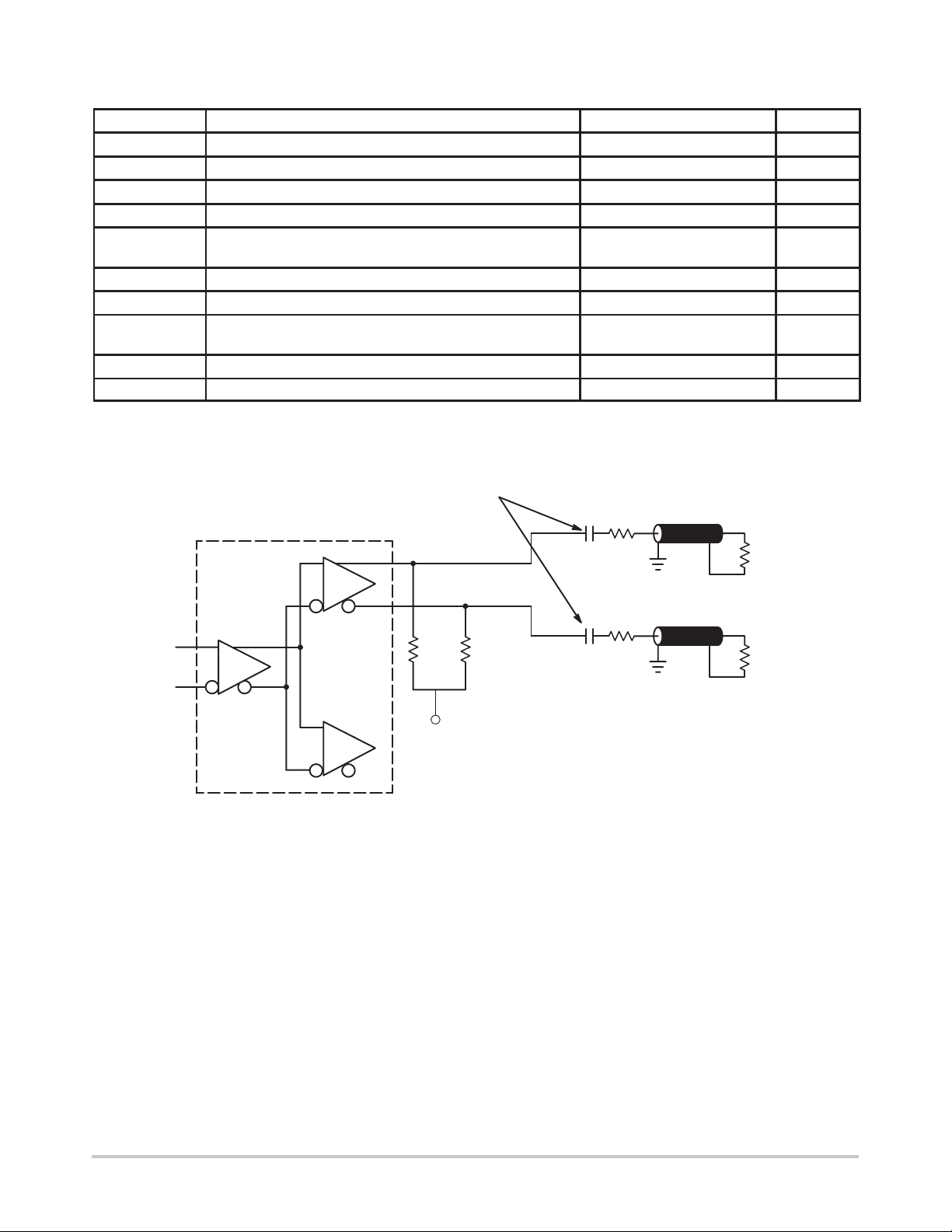
driving a coaxial cable, proper termination is required at both ends of
the line to minimize signal loss. The 1.6 (5V) and 1.4V (3.3V) swing
allow for termination at both ends of the cable, while maintaining a
800mV (5V) and 700mV (3.3V) swing at the receiving end of the
cable. Because of the larger output swings, the device cannot be
terminated into the standard VCC–2.0V. All of the DC parameters are
tested with a 50Ω to VCC–3.0V load. The driver accepts a standard
differential ECL input and can run off of the digital video broadcast
standard –5.0V supply .
http://onsemi.com
8
1
SO–8
D SUFFIX
CASE 751
• 310ps T ypical Propagation Delay
• 3.0 GHz T ypical Toggle Frequency
• 1.6V (5V) and 1.4V (3.3V) Swing
• PECL mode: 3.0V to 5.5V V
• ECL mode: 0V V
with VEE = –3.0V to –5.5V
CC
with VEE = 0V
CC
• Internal Input Resistors: Pulldown on D, Pulldown and Pullup on D
• Q Output will default LOW with inputs open or at V
EE
• ESD Protection: >4KV HBM, >200V MM
• New Differential Input Common Mode Range
• Moisture Sensitivity Level 1, Indefinite Time Out of Drypack
• Flammability Rating: UL–94 code V–0 @ 1/8”,
Oxygen Index 28 to 34
• Transistor Count = 152 devices
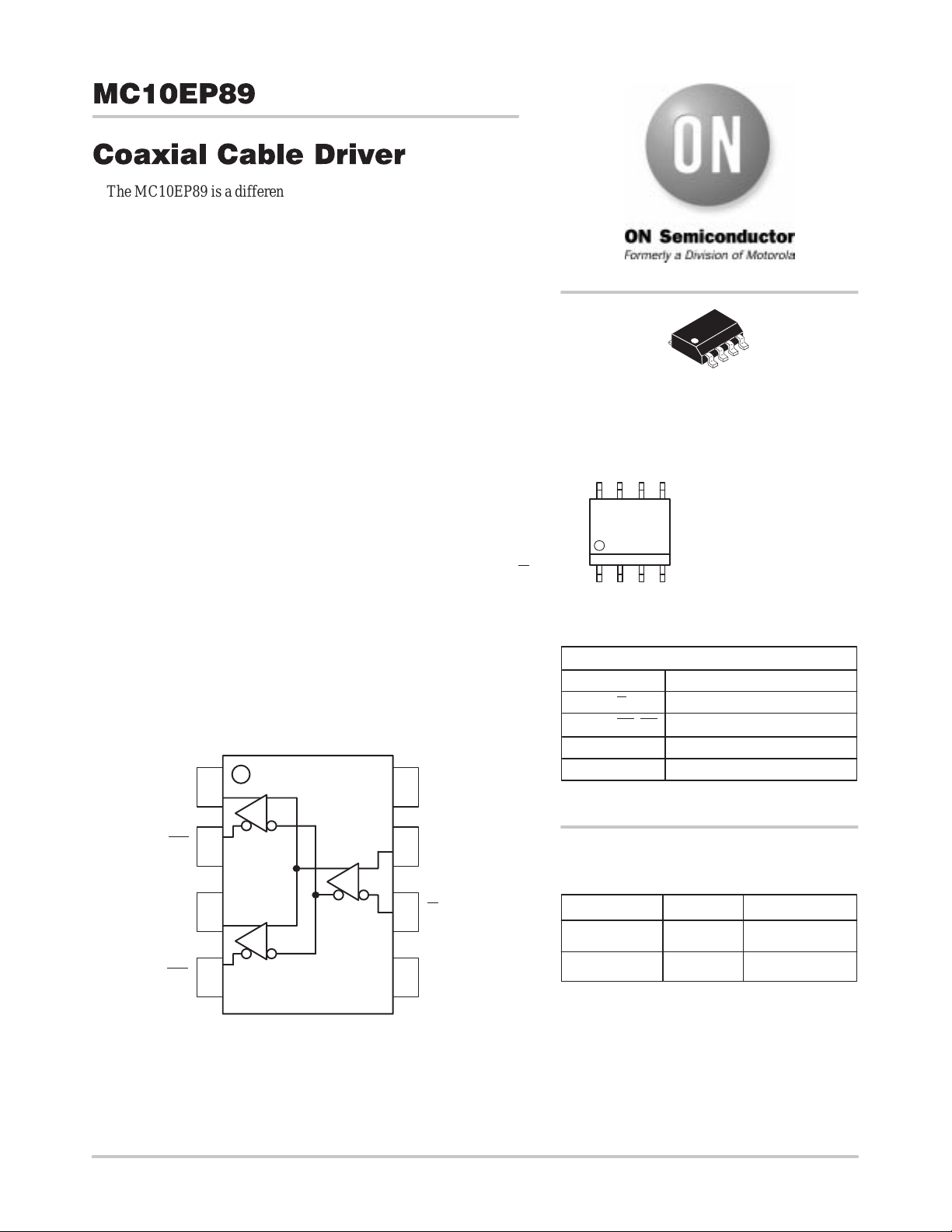
Q0
Q0
Q1
1
2
3
78D
6
V
CC
D
MARKING DIAGRAM
8
HEP89
ALYW
1
*For additional information, see Application Note
AND8002/D
PIN DESCRIPTION
PIN
D, D
Q0, Q1, Q0, Q1 ECL Data Outputs
V
CC
V
EE
ORDERING INFORMATION
Device Package Shipping
MC10EP89D SOIC 98 Units/Rail
A = Assembly Location
L = W afer Lot
Y = Year
W = Work Week
FUNCTION
ECL Data Inputs
Positive Supply
Negative, 0 Supply
45
Q1
Figure 1. 8–Lead Pinout (Top View) and Logic Diagram
Semiconductor Components Industries, LLC, 1999
December, 1999 – Rev. 1
V
EE
1 Publication Order Number:
MC10EP89DR2 SOIC 2500 Tape & Reel
MC10EP89/D
MC10EP89
MAXIMUM RATINGS*
Symbol Parameter Value Unit
V
EE
V
CC
V
I
V
I
I
out
T
A
T
stg
θ
JA
θ
JC
T
sol
* Maximum Ratings are those values beyond which damage to the device may occur.
Power Supply (VCC = 0V) –6.0 to 0 VDC
Power Supply (VEE = 0V) 6.0 to 0 VDC
Input Voltage (VCC = 0V, VI not more negative than VEE) –6.0 to 0 VDC
Input Voltage (VEE = 0V, VI not more positive than VCC) 6.0 to 0 VDC
Output Current Continuous
Surge
Operating Temperature Range –40 to +85 °C
Storage Temperature –65 to +150 °C
Thermal Resistance (Junction–to–Ambient) Still Air
500lfpm
Thermal Resistance (Junction–to–Case) 41 to 44 ± 5% °C/W
Solder Temperature (<2 to 3 Seconds: 245°C desired) 265 °C
DC BLOCKING CAPACITORS
75Ω
50
100
190
130
75Ω COAX
mA
°C/W
EP89
0.1µF
150Ω 150Ω
V
EE
0.1µF
Figure 2. EP89 T ermination Configuration
75Ω
75Ω
75Ω COAX
75Ω
http://onsemi.com
2
MC10EP89
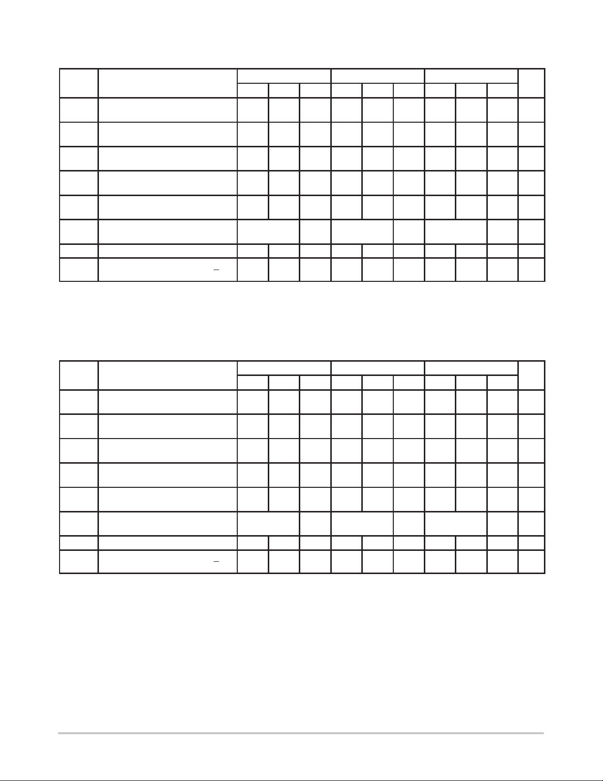
DC CHARACTERISTICS, ECL/LVECL (VCC = 0V; VEE = –3.3 ± 0.01V) (Note 4.)
–40°C 25°C 85°C
Symbol Characteristic Min Typ Max Min Typ Max Min Typ Max Unit
IEE
V
OH
V
OL
V
IH
V
IL
V
IHCMR
I
IH
I
IL
NOTE: 10EP circuits are designed to meet the DC specifications shown in the above table after thermal equilibrium has been established. The
1. VCC = 0V, VEE = –3.3V , all other pins floating.
2. All loading with 50 ohms to VCC–3.0 volts.
3. V
4. Input and output parameters vary 1:1 with VCC.
Power Supply Current
(Note 1.)
Output HIGH Voltage
(Note 2.)
Output LOW Voltage
(Note 2.)
Input HIGH Voltage
Single Ended
Input LOW Voltage
Single Ended
Input HIGH Voltage Common Mode
Range (Note 3.)
Input HIGH Current 150 150 150 µA
Input LOW Current D
circuit is in a test socket or mounted on a printed circuit board and transverse airflow greater than 500lfpm is maintained.
min varies 1:1 with VEE, max varies 1:1 with VCC.
IHCMR
D
22 28 34 24 32 38 28 34 40 mA
–1220 –1120 –1020 –1150 –1050 –950 –1075 –975 –875 mV
–2680 –2580 –2480 –2670 –2570 –2470 –2630 –2530 –2430 mV
–1230 –890 –1130 –810 –1060 –720 mV
–1950 –1500 –1950 –1480 –1950 –1445 mV
–1.3 0.0 –1.3 0.0 –1.3 0.0 V
0.5
–150
0.5
–150
0.5
–150
µA
DC CHARACTERISTICS, ECL/LVECL (VCC = 0V; VEE = –5.2 ± 0.01V) (Note 8.)
–40°C 25°C 85°C
Symbol Characteristic Min Typ Max Min Typ Max Min Typ Max Unit
IEE
V
OH
V
OL
V
IH
V
IL
V
IHCMR
I
IH
I
IL
NOTE: 10EP circuits are designed to meet the DC specifications shown in the above table after thermal equilibrium has been established. The
5. VCC = 0V, VEE = –5.2V , all other pins floating.
6. All loading with 50 ohms to VCC–3.0 volts.
7. V
8. Input and output parameters vary 1:1 with VCC.
Power Supply Current
(Note 5.)
Output HIGH Voltage
(Note 6.)
Output LOW Voltage
(Note 6.)
Input HIGH Voltage
Single Ended
Input LOW Voltage
Single Ended
Input HIGH Voltage Common Mode
Range (Note 7.)
Input HIGH Current 150 150 150 µA
Input LOW Current D
circuit is in a test socket or mounted on a printed circuit board and transverse airflow greater than 500lfpm is maintained.
min varies 1:1 with VEE, max varies 1:1 with VCC.
IHCMR
D
25 32 39 28 35 42 31 38 45 mA
–1220 –1120 –1020 –1150 –1050 –950 –1075 –975 –875 mV
–2950 –2800 –2650 –2950 –2850 –2650 –2950 –2800 –2650 mV
–1230 –890 –1130 –810 –1060 –720 mV
–1950 –1500 –1950 –1480 –1950 –1445 mV
–3.2 0.0 –3.2 0.0 –3.2 0.0 V
0.5
–150
0.5
–150
0.5
–150
µA
http://onsemi.com
3
 Loading...