

MC10EP57
4:1 Differential Multiplexer
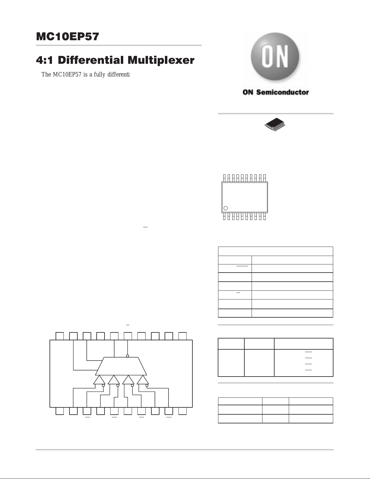
The MC10EP57 is a fully differential 4:1 multiplexer. By leaving
the SEL1 line open (pulled LOW via the input pulldown resistors) the
device can also be used as a differential 2:1 multiplexer with SEL0
input selecting between D0 and D1. The fully differential architecture
of the EP57 makes it ideal for use in low skew applications such as
clock distribution.
The SEL1 is the most significant select line. The binary number
applied to the select inputs will select the same numbered data input
(i.e., 00 selects D0).
Multiple VBB outputs are provided for single-ended or AC coupled
interfaces. In these scenarios, the VBB output should be connected to
the data bar inputs and bypassed via a 0.01µF capacitor to ground.
Note that the VBB output can source/sink up to 0.5mA of current
without upsetting the voltage level. All VCC and VEE pins must be
externally connected to power supply to guarantee proper operation
http://onsemi.com
20
1
TSSOP–20
DT SUFFIX
CASE 948E
MARKING DIAGRAM
• 350ps Typical Propagation Delays
• Typical Frequency 3.0GHz
• 20–Lead TSSOP Package
• PECL mode: 3.0V to 5.5V V
• ECL mode: 0V V
with VEE = –3.0V to –5.5V
CC
with VEE = 0V
CC
• Internal Input Resistors: Pulldown on D, D
• Q Output will default LOW with inputs open or at V
EE
• ESD Protection: >2KV HBM, >100V MM
• V
BB
Outputs
• New Differential Input Common Mode Range
• Moisture Sensitivity Level 1, Indefinite T ime Out of Drypack.
For Additional Information, See Application Note AND8003/D
• Useful as Either 4:1 or 2:1 Multiplexer
• Flammability Rating: UL–94 code V–0 @ 1/8”,
Oxygen Index 28 to 34
• T ransistor Count = 584 devices
SEL0
VCCSEL1
1920
V
CC
1718 16 15 14 13 12
Q
4:1
Q VCCV
BB1VBB2VEE
11
MC10
EP57
ALYW
*For additional information, see Application Note
AND8002/D
PIN DESCRIPTION
PIN
D0–3, D0–3
SEL0, 1 ECL Mux Select Inputs
V
, V
BB1
BB2
Q, Q
V
CC
V
EE
FUNCTION TABLE
SEL1
L
L
H
H
SEL0
A = Assembly Location
L = Wafer Lot
Y = Year
W = Work Week
FUNCTION
ECL Diff. Data Inputs
ECL Reference Output Voltage
ECL Data Outputs
Positive Supply
Negative, 0 Supply
DATA OUT
L
H
L
H
D0, D0
D1, D1
D2, D2
D3, D3
43
21
D0
CC
Figure 1. 20–Lead TSSOP (Top View) and Logic Diagram
Semiconductor Components Industries, LLC, 2000
April, 2000 – Rev. 2
56789
D1D1 D2D0
D2V
D3 V
ORDERING INFORMATION
Device Package Shipping
10
D3
EE
1 Publication Order Number:
MC10EP57DT TSSOP 75 Units/Rail
MC10EP57DTR2 TSSOP 2500 Tape & Reel
MC10EP57/D
MC10EP57
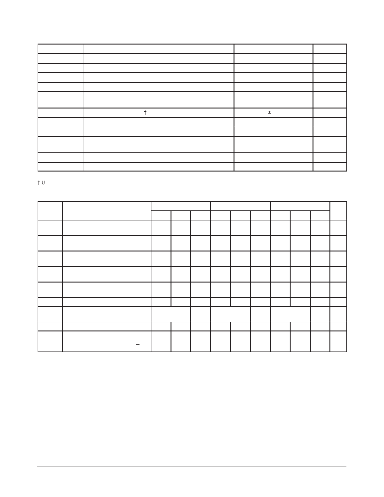
MAXIMUM RATINGS*
Symbol Parameter Value Unit
V
EE
V
CC
V
I
V
I
I
out
I
BB
T
A
T
stg
θ
JA
θ
JC
T
sol
* Maximum Ratings are those values beyond which damage to the device may occur.
{
Use for inputs of same package only.
DC CHARACTERISTICS, ECL/LVECL (VCC = 0V; VEE = –5.5V to –3.0V) (Note 4.)
Symbol Characteristic Min Typ Max Min Typ Max Min Typ Max Unit
IEE
V
OH
V
OL
V
IH
V
IL
V
BB
V
IHCMR
I
IH
I
IL
NOTE: 10EP circuits are designed to meet the DC specifications shown in the above table after thermal equilibrium has been established. The
1. VCC = 0V, VEE = V
2. All loading with 50 ohms to VCC–2.0 volts.
3. V
4. Input and output parameters vary 1:1 with VCC.
Power Supply Current
(Note 1.)
Output HIGH Voltage
(Note 2.)
Output LOW Voltage
(Note 2.)
Input HIGH Voltage
Single Ended
Input LOW Voltage
Single Ended
Output Voltage Reference –1550 –1450 –1350 –1500 –1400 –1300 –1450 –1350 –1250 mV
Input HIGH Voltage Common Mode
Range (Note 3.)
Input HIGH Current 150 150 150 µA
Input LOW Current
circuit is in a test socket or mounted on a printed circuit board and transverse airflow greater than 500lfpm is maintained.
min varies 1:1 with VEE, max varies 1:1 with VCC.
IHCMR
Power Supply (VCC = 0V) –6.0 to 0 VDC
Power Supply (VEE = 0V) 6.0 to 0 VDC
Input Voltage (VCC = 0V, VI not more negative than VEE) –6.0 to 0 VDC
Input Voltage (VEE = 0V, VI not more positive than VCC) 6.0 to 0 VDC
Output Current Continuous
VBB Sink/Source Current
Operating Temperature Range –40 to +85 °C
Storage Temperature –65 to +150 °C
Thermal Resistance (Junction–to–Ambient) Still Air
Thermal Resistance (Junction–to–Case) 23 to 41 ±5% °C/W
Solder Temperature (<2 to 3 Seconds: 245°C desired) 265 °C
SEL, D
to V
EEmin
EEmax
{
–40°C 25°C 85°C
40 52 65 40 52 65 40 52 65 mA
–1135 –1060 –885 –1070 –945 –820 –1010 –885 –760 mV
–1995 –1810 –1685 –1995 –1745 –1620 –1995 –1685 –1560 mV
–1210 –885 –1145 –820 –1085 –760 mV
–1935 –1610 –1870 –1545 –1810 –1485 mV
VEE+2.0 0.0 VEE+2.0 0.0 VEE+2.0 0.0 V
0.5
D
, all other pins floating.
–150
Surge
500lfpm
0.5
–150
50
100
± 0.5 mA
140
100
0.5
–150
mA
°C/W
µA
http://onsemi.com
2
MC10EP57
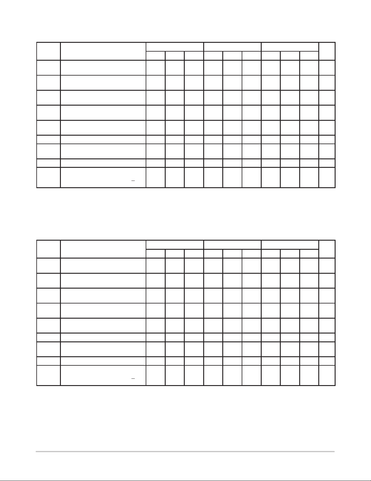
DC CHARACTERISTICS, LVPECL (VCC = 3.3V ± 0.3V, VEE = 0V) (Note 8.)
–40°C 25°C 85°C
Symbol Characteristic Min Typ Max Min Typ Max Min Typ Max Unit
IEE
V
OH
V
OL
V
IH
V
IL
V
BB
V
IHCMR
I
IH
I
IL
NOTE: 10EP circuits are designed to meet the DC specifications shown in the above table after thermal equilibrium has been established. The
5. VCC = 3.3V, VEE = 0V, all other pins floating.
6. All loading with 50 ohms to VCC–2.0 volts.
7. V
8. Input and output parameters vary 1:1 with VCC.
Power Supply Current
(Note 5.)
Output HIGH Voltage
(Note 6.)
Output LOW Voltage
(Note 6.)
Input HIGH Voltage
Single Ended
Input LOW Voltage
Single Ended
Output Voltage Reference 1750 1850 1950 1800 1900 2000 1850 1950 2050 mV
Input HIGH Voltage Common Mode
Range (Note 7.)
Input HIGH Current 150 150 150 µA
Input LOW Current
circuit is in a test socket or mounted on a printed circuit board and transverse airflow greater than 500lfpm is maintained.
min varies 1:1 with VEE, max varies 1:1 with VCC.
IHCMR
SEL, D
D
40 52 65 40 52 65 40 52 65 mA
2165 2240 2415 2230 2355 2480 2290 2415 2540 mV
1305 1490 1615 1305 1555 1680 1305 1615 1740 mV
2090 2415 2155 2480 2215 2540 mV
1365 1690 1430 1755 1490 1815 mV
2.0 3.3 2.0 3.3 2.0 3.3 V
0.5
–150
0.5
–150
0.5
–150
µA
DC CHARACTERISTICS, PECL (VCC = 5.0V ± 0.5V, VEE = 0V) (Note 12.)
–40°C 25°C 85°C
Symbol Characteristic Min Typ Max Min Typ Max Min Typ Max Unit
IEE
V
OH
V
OL
V
IH
V
IL
V
BB
V
IHCMR
I
IH
I
IL
NOTE: 10EP circuits are designed to meet the DC specifications shown in the above table after thermal equilibrium has been established. The
9. VCC = 5.0V, VEE = 0V, all other pins floating.
10.All loading with 50 ohms to VCC–2.0 volts.
11. V
12.Input and output parameters vary 1:1 with VCC.
Power Supply Current
(Note 9.)
Output HIGH Voltage
(Note 10.)
Output LOW Voltage
(Note 10.)
Input HIGH Voltage
Single Ended
Input LOW Voltage
Single Ended
Output Voltage Reference 3450 3550 3650 3500 3600 3700 3550 3650 3750 mV
Input HIGH Voltage Common Mode
Range (Note 11.)
Input HIGH Current 150 150 150 µA
Input LOW Current
circuit is in a test socket or mounted on a printed circuit board and transverse airflow greater than 500lfpm is maintained.
min varies 1:1 with VEE, max varies 1:1 with VCC.
IHCMR
SEL, D
D
40 52 65 40 52 65 40 52 65 mA
3865 3940 4115 3930 4055 4180 3990 4115 4240 mV
3005 3190 3315 3005 3255 3380 3005 3315 3440 mV
3790 4115 3855 4180 3915 4240 mV
3065 3390 3130 3455 3190 3515 mV
2.0 5.0 2.0 5.0 2.0 5.0 V
0.5
–150
0.5
–150
0.5
–150
µA
http://onsemi.com
3
 Loading...