

Motorola MC10175L, MC10175P, MC10175FN Datasheet

SEMICONDUCTOR TECHNICAL DATA
The MC10175 is a high speed, low power quint latch. It features five D type
latches with common reset and a common two–input clock. Data is transferred
on the negative edge of the clock and latched on the positive edge. The two
clock inputs are “OR”ed together.
Any change on the data input will be reflected at the outputs while the clock
is low. The outputs are latched on the positive transition of the clock. While the
clock is in the high state, a change in the information present at the data inputs
will not affect the output information. The reset input is enabled only when the
clock is in the high state.
PD= 400 mW typ/pkg (No Load)
tpd= 2.5 ns typ (Data to Output)
tr, tf= 2.0 ns typ (20%–80%)
LOGIC DIAGRAM
10
D0
D1
12
D2 2
13
D3
9
D4
5
6
C0
C1
7
RESET
11
D
C
R
DCQ
R
DCQ
R
DCQ
R
DCQ
R
Q0
14
Q
Q1
15
Q2
Q3
3
Q4
4
V
= PIN 1
CC1
V
= PIN 16
CC2
VEE= PIN 8
L SUFFIX
CERAMIC PACKAGE
CASE 620–10
P SUFFIX
PLASTIC PACKAGE
CASE 648–08
FN SUFFIX
PLCC
CASE 775–02
DIP
PIN ASSIGNMENT
V
CC1
Q2
Q3
Q4
D4
C0
C1
V
EE
Pin assignment is for Dual–in–Line Package.
For PLCC pin assignment, see the Pin Conversion
T ables on page 6–11 of the Motorola MECL Data
1
2
3
4
5
6
7
8
Book (DL122/D).
16
15
14
13
12
11
10
V
CC2
Q1
Q0
D2
D1
RESET
D0
D3
9
3/93
Motorola, Inc. 1996
TRUTH TABLE
D C0 C1 Reset Q
L L L X L
H L L X H
X H X L Q n
X X H L Q n
X H X H L
X X H H L
3–126
n+1
REV 5
MC10175
Under
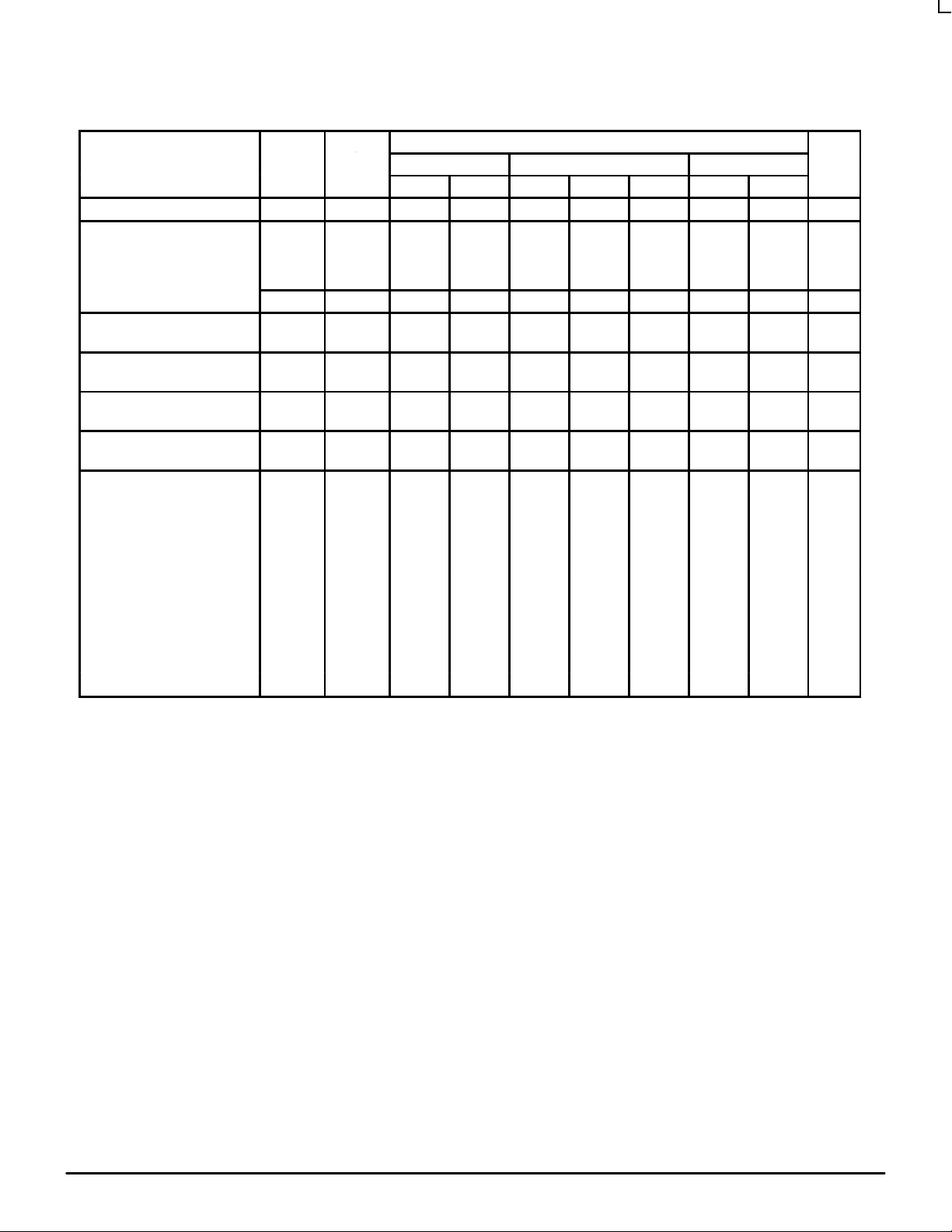
ELECTRICAL CHARACTERISTICS
Test Limits
Pin
Characteristic Symbol
Power Supply Drain Current I
Input Current I
Output Voltage Logic 1 V
Output Voltage Logic 0 V
Threshold Voltage Logic 1 V
Threshold Voltage Logic 0 V
Switching Times (50Ω Load) ns
Data Input t
Clock Input t
Reset Input t
Setup TIme
Hold Time
Rise Time (20 to 80%) t+ 14 1.0 3.6 1.1 3.5 1.1 3.7
Fall Time (20 to 80%) t– 14 1.0 3.6 1.1 3.5 1.1 3.7
1. Individually test each input; apply V
2. Output latched to high logic state prior to test.
E
inH
I
inL
OH
OL
OHA
OLA
10+14+
t
10–14–
6–14+
t
6–14–
11+4–
t
11+14–
t
setup
t
hold
ILmin
Under
Test
8 107 78 97 107 mAdc
6
7
10
11
All 0.5 0.5 0.3 µAdc
14
15
14
15
14
15
14
15
14
14
14
14
4
14
14
14
to pin under test.
–30°C +25°C +85°C
Min Max Min Typ Max Min Max
–1.060
–1.060
–1.890
–1.890
–1.080
–1.080
1.0
1.0
1.0
1.0
1.0
1.0
2.5
1.5
460
460
460
1000
–0.890
–0.890
–1.675
–1.675
–1.655
–1.655
3.6
3.6
4.7
4.7
4.0
4.0
–0.960
–0.960
–1.850
–1.850
–0.980
–0.980
1.0
1.0
1.0
1.0
1.0
1.0
2.5
1.5
290
290
290
650
–0.810
–0.810
–1.650
–1.650
–1.630
–1.630
3.5
3.5
4.3
4.3
3.9
3.9
–0.890
–0.890
–1.825
–1.825
–0.910
–0.910
1.0
1.0
1.0
1.0
1.0
1.0
2.5
1.5
–0.700
–0.700
–1.615
–1.615
–1.595
–1.595
290
290
290
650
3.6
3.6
4.4
4.4
4.2
4.2
Unit
µAdc
Vdc
Vdc
Vdc
Vdc
DL122 — Rev 6
3–127 MOTOROLAMECL Data
 Loading...