

Motorola MC10141P, MC10141FN, MC10141L Datasheet
SEMICONDUCTOR TECHNICAL DATA
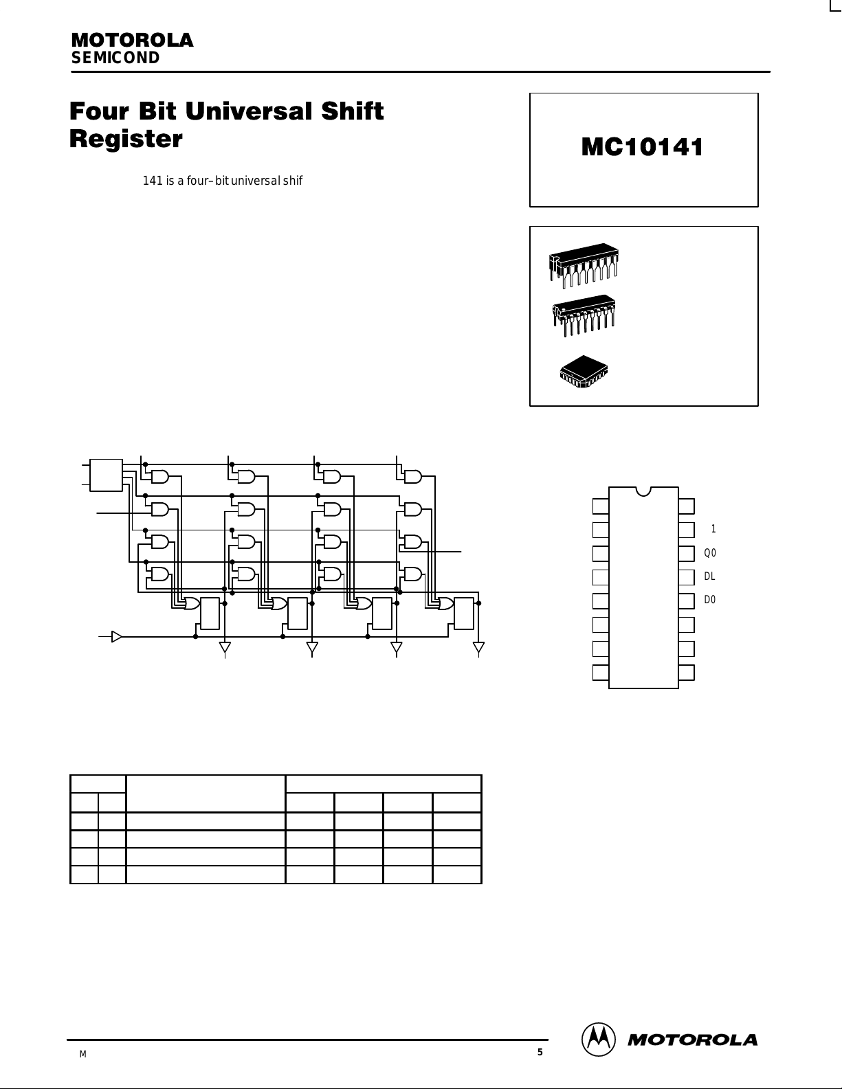
The MC10141 is a four–bit universal shift register which performs shift left, or
shift right, serial/parallel in, and serial/parallel out operations with no external
gating. Inputs S1 and S2 control the four possible operations of the register
without external gating of the clock. The flip–flops shift information on the
positive edge of the clock. The four operations are stop shift, shift left, shift right,
and parallel entry of data. The other six inputs are all data type inputs; four for
parallel entry data, and one for shifting in from the left (DL) and one for shifting
in from the right (DR).
PD= 425 mW typ/pkg (No Load)
f
= 200 MHz typ
Shift
tr, tf= 2.0 ns typ (20%–80%)
LOGIC DIAGRAM
D3
S1
1 of 4
Decoder
S2
DR
C
SELECT OUTPUTS
S1 S2 OPERATING MODE Q0
L L Parallel Entry D0 D1 D2 D3
L H Shift Right* Q1
H L Shift Left* DL Q0
H H Stop Shift Q0
*Outputs as exist after pulse appears at “C” input with input conditions as
shown. (Pulse = Positive transition of clock input).
Parallel Enter
Shift Right
Shift Left
Hold
D2 D1 D0
Q
D
C
Q3
Q
D
C
Q2 Q1 Q0
TRUTH TABLE
Q1
n+1
Q2
n
Q1
n
n+1
n
n
n
Q
D
C
V
CC1
V
CC2
VEE= PIN 8
Q2
n+1
Q3
n
Q1
n
Q2
n
D
C
= PIN 1
= PIN 16
Q3
n+1
DR
Q2
n
Q3
n
DL
Q
L SUFFIX
CERAMIC PACKAGE
CASE 620–10
P SUFFIX
PLASTIC PACKAGE
CASE 648–08
FN SUFFIX
PLCC
CASE 775–02
DIP
PIN ASSIGNMENT
V
CC1
Q2
Q3
DR
D3
S2
V
EE
Pin assignment is for Dual–in–Line Package.
For PLCC pin assignment, see the Pin Conversion
T ables on page 6–11 of the Motorola MECL Data
C
1
2
3
4
5
6
7
8
Book (DL122/D).
16
15
14
13
12
11
10
V
CC2
Q1
Q0
DL
D0
D1
S1
D2
9
3/93
Motorola, Inc. 1996
3–46
REV 5
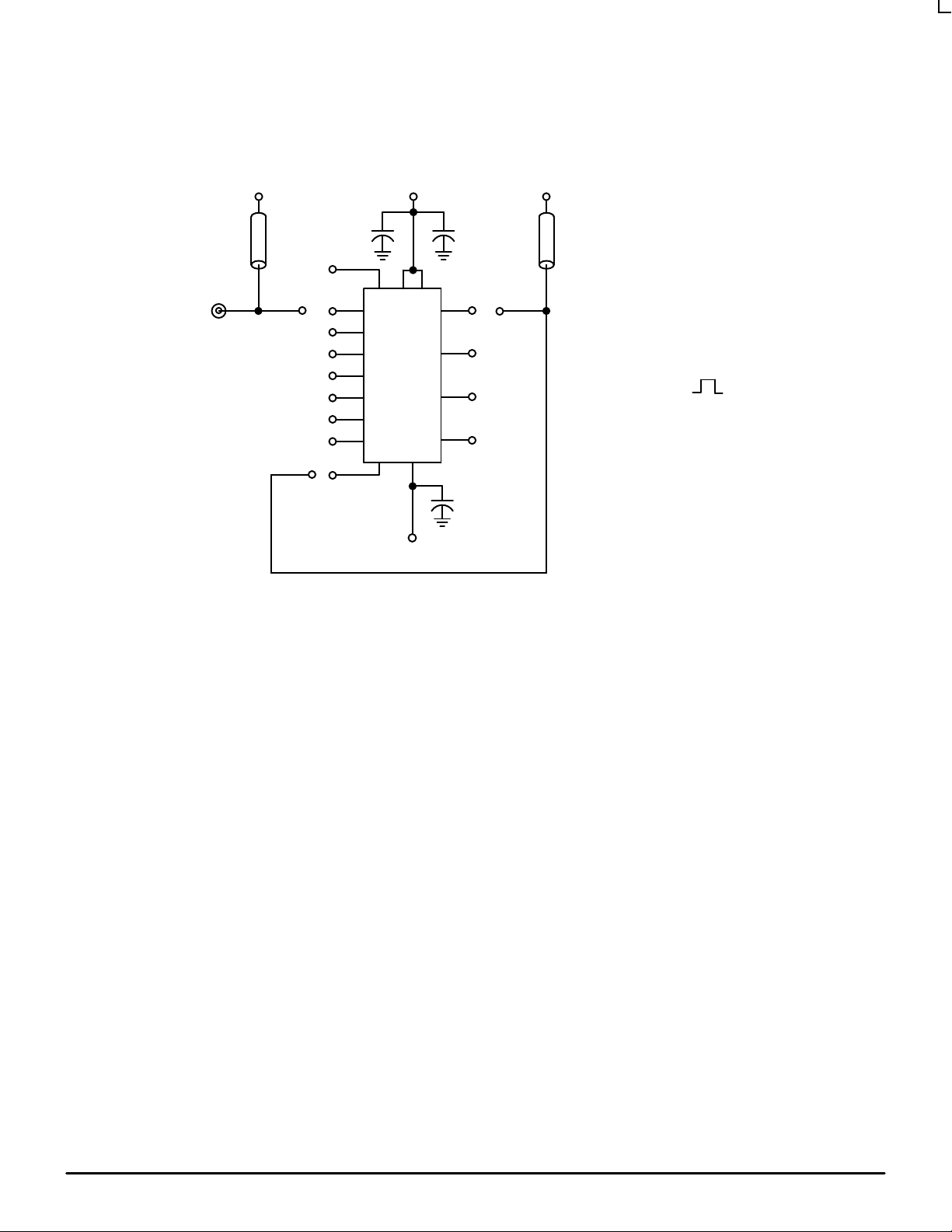
V
IN
COAX
INPUT
PULSE GENERAT OR
50–ohm termination to ground
located in each scope channel input.
SHIFT FREQUENCY TEST CIRCUIT
V
= V
CC1
CC2
25 uF
C
D0
D1
D2
D3
S1
S2
DR
DL
+2.0 VDC
16
1
Q0
Q1
Q2
Q3
8
0.1
0.1
µ
F
µ
F
V
OUT
MC10141
All input and output cables to the
scope are equal lengths of 50–ohm
coaxial cable. Wire length should be
Coax
TEST PROCEDURES:
1. SET D1, D2, D3 = +0.31 VDC (LOGIC L)
2. APPY CLOCK PULSE TO SET Q0 HIGH.
3. MAINTAIN CLOCK LOW.
SET S1 = +0.31 VDC (LOGIC L)
4. TEST SHIFT FREQUENCY
< 1/4 inch from TPin to input pin and
TP
to output pin.
out
D0 = +1.11 VDC (LOGIC H)
S2 = +1.11 VDC (LOGIC H)
—
V
IH
V
IL
VEE = –3.2VDC
DL122 — Rev 6
3–47 MOTOROLAMECL Data
 Loading...