

MAX1617
SMBus Temperature Sensor
with Internal and External
Diode Input
The MAX1617 is a serially programmable temperature sensor
optimized for monitoring modern high performance CPUs with
on–board, integrated temperature sensing diodes. Temperature data is
converted from the CPU’s diode outputs and made available as an
8–bit digital word.
Communication with the MAX1617 is accomplished via the
standard System Management Bus (SMBus) commonly used in
modern computer systems. This permits reading the current
internal/external temperature, programming the threshold setpoints,
and configuring the device. Additionally, an interrupt is generated on
the ALERT pin when temperature moves outside the preset threshold
windows in either direction.
A Standby command may be sent via the SMBus by signaling the
STBY input to activate the low–power Standby mode. Registers can
be accessed while in Standby mode. Address selection inputs allow up
to nine MAX1617s to share the same 2–wire SMBus for multi–zone
monitoring.
All registers can be read by the host, and both polled and interrupt
driven systems are easily accommodated. Small size, low installed
cost, and ease of use make the MAX1617 an ideal choice for
implementing sophisticated system management schemes, such as
ACPI.
Features
• Includes Internal and External Sensing Capability
• Outputs T emperature As 8–Bit Digital Word
• Solid State T emperature Sensing; 1°C Resolution
• 3.0 — 5.5V Operating Range
• Independent Internal and External Threshold Set–Points With
ALERT Interrupt Output
• SMBus 2–Wire Serial Interface
• Up T o 9 MAX1617s May Share the Same Bus
• Low Standby Power Mode
• Low Power: 70 µA (max) Operating, 10 µA (max) Standby Mode
• 16–Pin Plastic QSOP Package
• Operating T emperature Range: –55°C to +125°C
http://onsemi.com
16–Pin QSOP
DB SUFFIX
PRELIMINARY INFORMATION
ADD1
ORDERING INFORMATION
Device Package Shipping
MAX1617DBR2 16–Pin QSOP 2500 Tape/Reel
CASE TBD
PIN CONFIGURATION
(Top View)
NC
V
DD
D
D
NC
GND
GND
+
–
1
2
3
4
MAX1617
5
6
7
8
16
15
14
13
12
11
10
9
NC
STBY
SCL
NC
SDA
ALERT
ADD0
NC
Typical Applications
• Thermal Protection For Intel “Deschutes” Pentium II and Other
High Performance CPUs with Integrated On–Board Diode - No
Sensor Mounting Problems!
• Accurate T emperature Sensing From Any Silicon Junction Diode
• Thermal Management in Electronic Systems: Computers, Network
Equipment, Power Supplies
Semiconductor Components Industries, LLC, 1999
February , 2000 – Rev. 0
1 Publication Order Number:
MAX1617/D
MAX1617
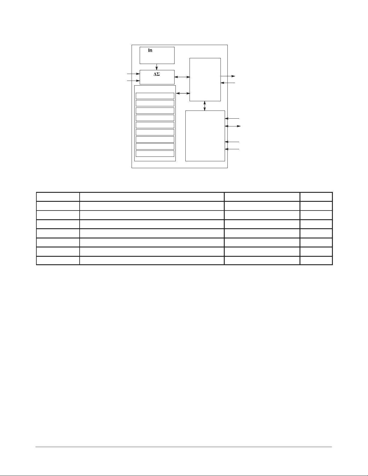
FUNCTIONAL BLOCK DIAGRAM
Internal
Sensor
(Diode)
+
D
–
D
ABSOLUTE MAXIMUM RATINGS*
Symbol Parameter Value Unit
V
DD
T
A
T
stg
P
D
* Maximum Ratings are those values beyond which damage to the device may occur.
Power Supply Voltage 6.0 V
Voltage on Any Pin (GND – 0.3 V) to (VDD + 0.3 V) V
Operating Temperature Range –55 to +125 °C
Storage Temperature Range –65 to +150 °C
SMBus Input/Output Current –1 to +50 mA
D– Input Current ±1 mA
Maximum Power Dissipation 330 mW
DS
Modulator
Register Set
Int. Temp
Ext.Temp
Status Byte
Config. Byte
Conv. Rate
Ext. Hi Limit
Ext. Lo Limit
Int. Hi Limit
Int. Lo Limit
Control
Logic
SMBus
Interface
ALERT
STBY
SCL
SDA
ADD 0
ADD 1
http://onsemi.com
2
MAX1617
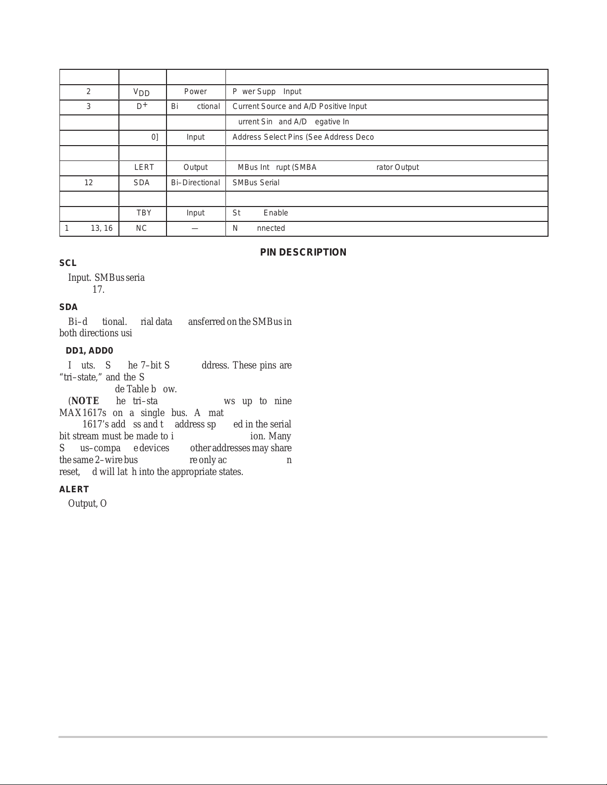
PIN DESCRIPTION
Pin No. Symbol Type Description
2
3
4
6, 10
7, 8
11
12
14
15
1, 5, 9, 13, 16
SCL
Input. SMBus serial clock. Clocks data into and out of the
MAX1617.
SDA
Bi–directional. Serial data is transferred on the SMBus in
both directions using this pin.
ADD1, ADD0
Inputs. Sets the 7–bit SMBus address. These pins are
“tri–state,” and the SMBus addresses are specified in the
Address Decode Table below.
(NOTE: The tri–state scheme allows up to nine
MAX1617s on a single bus. A match between the
MAX1617’s address and the address specified in the serial
bit stream must be made to initiate communication. Many
SMBus–compatible devices with other addresses may share
the same 2–wire bus. These pins are only active at power–on
reset, and will latch into the appropriate states.
ALERT
Output, Open Collector, Active Low. The ALERT output
corresponds to the general SMBALER T signal and indicates
an interrupt event. The MAX1617 will respond to the
standard SMBus Alert Response Address when ALERT is
asserted. Normally , the ALERT output will be asserted when
any of the following occurs:
INT_TEMP equal to or exceeds INT_HLIM
INT_TEMP falls below INT_LLIM
EXT_TEMP equal to or exceeds EXT_HLIM
EXT_TEMP falls below EXT_LLIM
External Diode “Open”
The operation of the ALERT output is controlled by the
MASK1 bit in the CONFIG register . If the MASK1 bit is set
to “1,” no interrupts will be generated on ALERT. The
ALERT output is cleared and re–armed by the Alert
Response Address (ARA). This output may be
WIRE–ORed with similar outputs from other SMBus
devices. If the alarm condition persists after the ARA, the
ALERT output will be immediately re–asserted.
V
DD
+
D
–
D
ADD[1:0]
GND
ALERT
SDA
SCL
STBY
NC
Power
Bi–Directional
Bi–Directional
Input
Power
Output
Bi–Directional
Input
Input
—
Power Supply Input
Current Source and A/D Positive Input
Current Sink and A/D Negative Input
Address Select Pins (See Address Decode Table)
System Ground
SMBus Interrupt (SMBALERT) or Comparator Output
SMBus Serial Data
SMBus Serial Clock
Standby Enable
Not Connected
PIN DESCRIPTION
(NOTE: A pull–up resistor is necessary on ALERT since
it is an open–drain output. Current sourced from the pull–up
resistor causes power dissipation and may cause internal
heating of the MAX1617. T o avoid affecting the accuracy of
internal temperature readings, the pull–up resistors should
be made as large as possible.)
STBY
Input. The activation of Standby mode may be achieved
using either the STBY pin or the CHIP STOP bit (CONFIG
register). If STBY is pulled low, the MAX1617
unconditionally enters its low–power Standby mode. The
temperature–to–digital conversion process is halted, but
ALERT remains functional. The MAX1617’s bus interface
remains active, and all registers may be read from and
written to normally. The INT_TEMP and EXT_TEMP
registers will contain whatever data was valid at the time of
Standby. (Transitions on SDA or SCL due to external bus
activity may increase the Standby power consumption.)
+
D
Bi–directional. this pin connects to the anode of the
external diode and is the positive A/D input. Current is
injected into the external diode from the MAX1617, and the
temperature proportional V
digital temperature data.
—
D
Bi–directional. This pin connects to the cathode of the
external diode. Current is sunk from the external diode into
the MAX1617 through this pin. It also is the negative input
terminal to the MAX1617’s A/D converter . This node is kept
at approximately 0.7V above GROUND.
V
DD
Input. Power supply input. See electrical specifications.
GND
Input. Ground return for all MAX1617 functions.
is measured and converted to
BE
http://onsemi.com
3
MAX1617
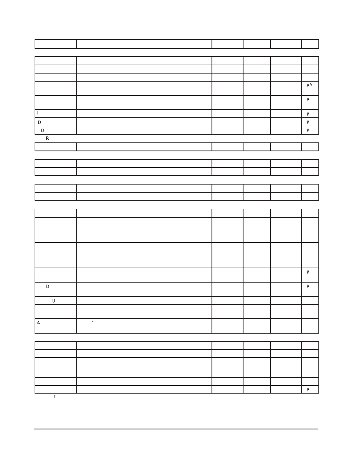
DC ELECTRICAL CHARACTERISTICS (VDD = 3.3 V, –55°C ≤ TA ≤ 125°C, unless otherwise noted.)
Symbol
Power Supply
V
DD
V
UV–LOCK
V
POR
I
DD
I
DD
I
DD–STANDBY
I
DD–STANDBY
I
ADD–BIAS
ALERT Output
V
OL
ADD[1:0] Inputs
V
IL
V
IH
STBY Input
V
IL
V
IH
Temp–to–Bits Converter
T
RES
T
IERR
T
EERR
I
DIODE–HIGH
I
DIODE–LOW
V
D–SOURCE
t
CONV
D
CR
2–Wire SMBus Interface
V
IH
V
IL
V
OL
C
IN
I
LEAK
1. Operating current is an average value (including external diode injection pulse current) integrated over multiple conversion cycles. Transient
current may exceed this specification.
2. For true recurring conversion time see Conversion Rate register description.
3. Output current should be minimized for best temperature accuracy. Power dissipation within the MAX1617 will cause self–heating and
temperature drift error.
Power Supply Voltage 3.0 — 5.5 V
VDD Undervoltage Lockout Threshold 2.4 2.80 2.95 V
Power–On Reset Threshold (VDD Falling Edge) 1.0 1.7 2.3 V
Operating Current
0.25 Conv./Sec Rate SMBus Inactive
Operating Current
2 Conv./Sec Rate SMBus Inactive
Standby Supply Current (SMBus Active) — — 100
Standby Supply Current (SMBus Inactive) — — 10
ADD[1:0] Bias Current (Power–Up Only) — 160 —
Output Low Voltage (IOL = 1.0 mA)
Logic Input Low — — VDD x 0.3 V
Logic Input High VDD x 0.7 — — V
Logic Input Low — — VDD x 0.3 V
Logic Input High VDD x 0.7 — — V
Basic Temperature Resolution — 1.0 — °C
Internal Diode Temperature
+60°C ≤ TA ≤ +100°C
0°C ≤ TA ≤ +125°C
–55°C ≤ TA ≤ 0°C
External Diode Temperature
+60°C ≤ TA ≤ +100°C
0°C ≤ TA ≤ +125°C
–55°C ≤ TA ≤ 0°C
External Diode High Source Current
(D+) – (D–) ~ 0.65 V
External Diode Low Source Current
(D+) – (D–) ~ 0.65 V
Source Voltage — 0.7 — V
Conversion Time
From CHIP STOP to Conv. Complete
Conversion Rate Accuracy
(See Conversion Rate Register Desc.)
Logic Input High 2.2 — — V
Logic Input Low — — 0.8 V
SDA Output Low
IOL = 2 mA
IOL = 4 mA
Input Capacitance SDA, SCL — 5.0 — pF
I/O Leakage –1.0 0.1 1.0
(3)
(3)
Characteristic Min Typ Max Unit
m
m
m
m
m
°C
°C
m
m
m
A
A
A
A
A
A
A
V
A
(3)
(1)
(1)
(2)
— — 70
— — 180
— — 0.4 V
–2
–3
—
–3
–5
—
— 100 —
— 10 —
54 83 112 msec
–35 — +35 %
—
—
—
—
±3
—
—
±5
—
—
+2
+3
—
+3
+5
—
0.4
0.6
http://onsemi.com
4
 Loading...