

Motorola MAC321-4, MAC321-8, MAC321-6, MAC321-10 Datasheet
1
Motorola Thyristor Device Data
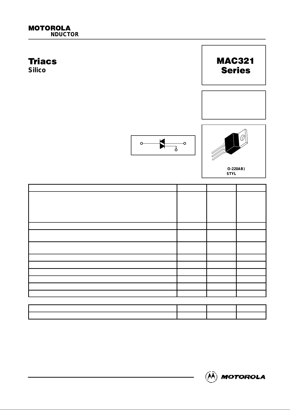
Triacs
Silicon Bidirectional Thyristors
. . . designed for full-wave ac control applications primarily in industrial environments
needing noise immunity.
• Guaranteed High Commutation Voltage
dv/dt — 500 V/µs Min @ TC = 25°C
• High Blocking Voltage — V
DRM
to 800 V
• Photo Glass Passivated Junction for Improved Power Cycling Capability and
Reliability
MAXIMUM RATINGS
(TC = 25°C unless otherwise noted.)
Rating
Symbol Value Unit
Peak Repetitive Off-State Voltage
(1)
(TJ = –40 to +125°C,
1/2 Sine Wave 50 to 60 Hz, Open Gate)
MAC321-4
MAC321-6
MAC321-8
MAC321-10
V
DRM
200
400
600
800
Volts
Peak Gate Voltage V
GM
10 Volts
On-State Current RMS (TC = +75°C
Full Cycle Sine Wave 50 to 60 Hz)
I
T(RMS)
20 Amp
Peak Surge Current (One Full Cycle, 60 Hz, TC = +75°C
preceded and followed by Rated Current)
I
TSM
150 Amp
Circuit Fusing Considerations (t = 8.3 ms) I2t 93 A2s
Peak Gate Power (TC = +75°C, Pulse Width = 2.0 µs) P
GM
20 Watts
Average Gate Power (TC = +75°C, t = 8.3 ms) P
G(AV)
0.5 Watt
Peak Gate Current I
GM
2.0 Amp
Operating Junction Temperature Range T
J
–40 to +125 °C
Storage Temperature Range T
stg
–40 to +150 °C
THERMAL CHARACTERISTICS
Characteristic Symbol Max Unit
Thermal Resistance, Junction to Case R
θJC
1.8 °C/W
1. V
DRM
for all types can be applied on a continuous basis. Blocking voltages shall not be tested with a constant current source such that the
voltage ratings of the devices are exceeded.
Order this document
by MAC321/D
MOTOROLA
SEMICONDUCTOR TECHNICAL DATA
Motorola, Inc. 1995
MAC321
Series
CASE 221A-04
(TO-220AB)
STYLE 4
TRIACs
20 AMPERES RMS
200 thru 800 VOLTS
MT1
G
MT2
2 Motorola Thyristor Device Data
ELECTRICAL CHARACTERISTICS
(TC = 25°C unless otherwise noted.)
Characteristic
Symbol Min Typ Max Unit
Peak Blocking Current
(VD = Rated V
DRM
, Gate Open)
TJ = 25°C
TJ = +125°C
I
DRM
—
—
—
—
10
2.0
µA
mA
Peak On-State Voltage (Either Direction)
(ITM = 28 A Peak; Pulse Width p 2.0 ms, Duty Cycle p 2.0%)
V
TM
— 1.4 1.7 Volts
Gate Trigger Current (Continuous dc)
(Main Terminal Voltage = 12 Vdc, RL = 100 Ohms)
MT2(+), G(+)
MT2(+), G(–)
MT2(–), G(–)
I
GT
—
—
—
—
—
—
100
100
100
mA
Gate Trigger Voltage (Continuous dc)
(Main Terminal Voltage = 12 Vdc, RL = 100 Ohms)
MT2(+), G(+)
MT2(+), G(–)
MT2(–), G(–)
(Main Terminal Voltage = Rated V
DRM
, RL = 10 kΩ, TJ = +125°C)
MT2(+), G(+); MT2(–), G(–); MT2(+), G(–)
V
GT
—
—
—
0.2
—
—
—
—
2.0
2.0
2.0
—
Volts
Holding Current (Either Direction)
(Main Terminal Voltage = 12 Vdc, Gate Open,
Initiating Current = 200 mA)
I
H
— — 100 mA
Turn-On Time
(VD = Rated V
DRM
, ITM = 28 A, IGT = 120 mA,
Rise Time = 0.1 µs, Pulse Width = 2.0 µs)
t
gt
— 1.5 — µs
Critical Rate of Rise of Off-State Voltage
(VD = Rated V
DRM
, Exponential Voltage Rise, Gate Open)
TJ = 25°C
TJ = +125°C
dv/dt(s)
500
200
—
—
—
—
V/µs
110
120
130
2 4 6 8 10 12
60
70
80
90
100
14 16
dc
0
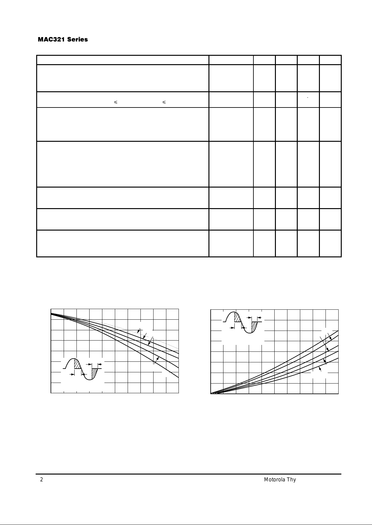
Figure 1. RMS Current Derating
5
40
35
30
25
20
15
10
2018
Figure 2. On-State Power Dissipation
I
T(RMS)
, RMS ON-STATE CURRENT (AMP)
50
0
2 4 6 8 10 12 14 160 2018
I
T(RMS)
, RMS ON-STATE CURRENT (AMP)
α
= 30
°
60
°
90
°
180
°
α
= CONDUCTION
ANGLE
α
α
α
= CONDUCTION
ANGLE
α
α
P
D(AV)
, AVERAGE POWER (WATT)
T
C
, MAXIMUM ALLOWABLE CASE TEMPERATURE ( C)
°
180
°
dc
90
°
60
°
α
= 30
°
TYPICAL CHARACTERISTICS
 Loading...