

MOTOROLA
查询MAC223A6FP/D供应商
SEMICONDUCTOR TECHNICAL DATA
Triacs
Silicon Bidirectional Triode Thyristors
. . . designed primarily for full-wave ac control applications, such as lighting systems,
heater controls, motor controls and power supplies; or wherever full–wave silicon–
gate–controlled devices are needed.
• Off–State Voltages to 800 Volts
• All Diffused and Glass Passivated Junctions for Parameter Uniformity and Stability
• Small, Rugged Thermowatt Construction for Thermal Resistance and High Heat
Dissipation
• Gate Triggering Guaranteed in Four Modes
Order this document
by MAC223A6FP/D
MAC223AFP
Series
ISOLATED TRIACs
THYRISTORS
25 AMPERES RMS
400 thru 800 VOL TS
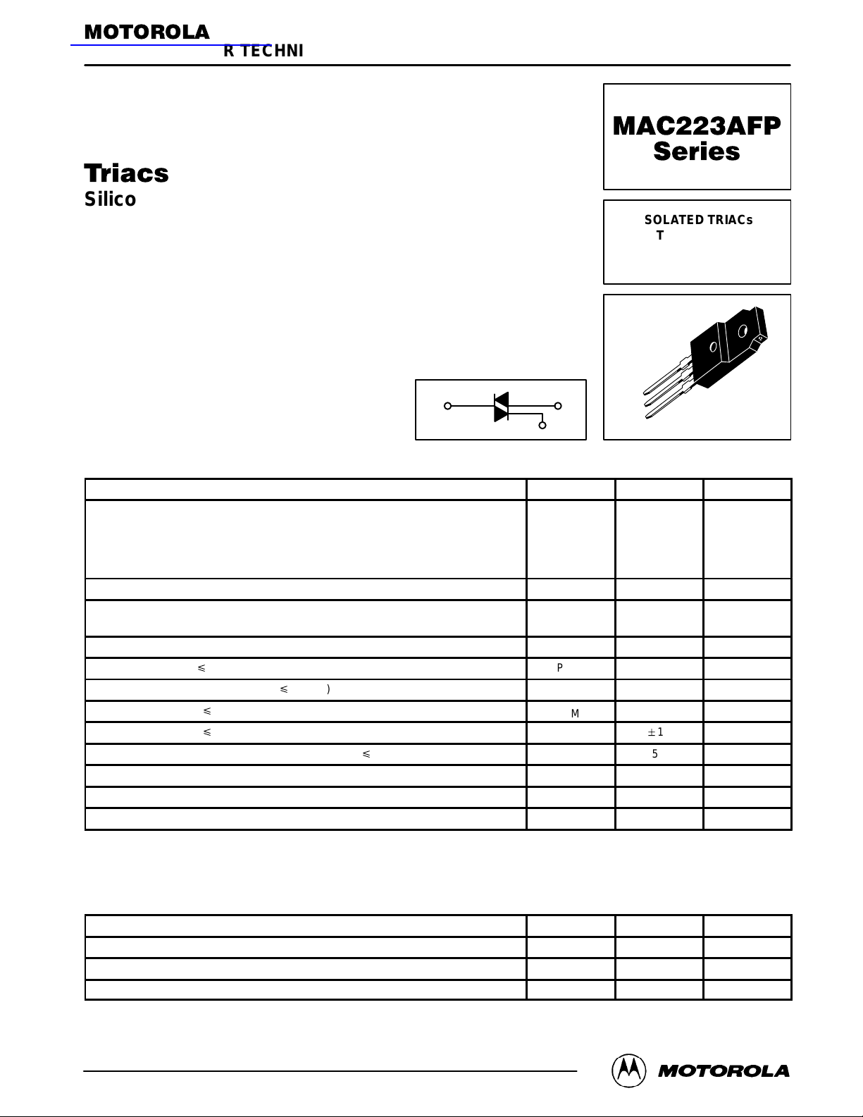
MT2
MAXIMUM RATINGS
Peak Repetitive Off-State Voltage
1/2 Sine Wave 50 to 60 Hz, Gate Open)
On-State RMS Current (TC = +80°C) Full Cycle Sine Wave 50 to 60 Hz
Peak Nonrepetitive Surge Current (One Full Cycle, 60 Hz, TC = 80°C,
preceded and followed by rated current)
Circuit Fusing (t = 8.3 ms) I2t 260 A2s
Peak Gate Power (t p 2 µs) P
Average Gate Power (TC = +80°C, t p 8.3 ms) P
Peak Gate Current (t p 2 µs) I
Peak Gate Voltage (t p 2 µs) V
RMS Isolation Voltage (TA = 25°C, Relative Humidity p 20%) V
Operating Junction Temperature T
Storage Temperature Range T
Mounting Torque — 8 in. lb.
1. V
2. The case temperature reference point for all TC measurements is a point on the center lead of the package as close as possible to the plastic
for all types can be applied on a continuous basis. Blocking voltages shall not be tested with a constant current source such that the
DRM
voltage ratings of the devices are exceeded.
body.
(TJ = 25°C unless otherwise noted.)
Rating
(1)
(TJ = –40 to +125°C,
MAC223A6FP
MAC223A8FP
MAC223A10FP
(2)
MT1
G
Symbol Value Unit
V
DRM
I
T(RMS
I
TSM
GM
G(AV)
GM
GM
(ISO
J
stg
MT1
MT2
G
400
600
800
25 Amps
250 Amps
20 Watts
0.5 Watt
2 Amps
"
1500 Volts
–40 to +125 °C
–40 to +150 °C
CASE 221C-02
STYLE 3
10 Volts
Volts
THERMAL CHARACTERISTICS
Characteristic Symbol Max Unit
Thermal Resistance, Junction to Case R
Thermal Resistance, Case to Sink R
Thermal Resistance, Junction to Ambient R
θJC
θCS
θJA
1.2 °C/W
2.2 °C/W
60 °C/W
Motorola Thyristor Device Data
Motorola, Inc. 1999
1
ELECTRICAL CHARACTERISTICS
Characteristic
Peak Blocking Current(1) TJ = 25°C
(VD = Rated V
Peak On-State Voltage
(ITM = 35 A Peak, Pulse Width p 2 ms, Duty Cycle p 2%)
Gate Trigger Current (Continuous dc)
(VD = 12 V, RL = 100 Ω)
MT2(+), G(+); MT2(–), G(–); MT2(+), G(–)
MT2(–), G(+)
Gate Trigger Voltage (Continuous dc)
(VD = 12 V, RL = 100 Ω)
MT2(+), G(+); MT2(–), G(–); MT2(+), G(–)
MT2(–), G(+)
(VD = Rated V
MT(+), G(+); MT2(–), G(–); MT2(+), G(–)
MT2(–), G(+)
Holding Current
(VD = 12 V, ITM = 200 mA, Gate Open)
Gate Controlled Turn–On Time
(VD = Rated V
Critical Rate of Rise of Off–State V oltage
(VD = Rated V
Critical Rate of Rise of Commutation Voltage
(VD = Rated V
di/dt = 12.6 A/ms, Gate Unenergized, TC = 80°C)
1. Ratings apply for open gate conditions. Devices shall not be tested with a constant current source for blocking voltage such that the voltage
applied exceeds the rated blocking voltage.
, Gate Open) TJ = 125°C
DRM
, TJ = 125°C, RL = 10 k)
DRM
, ITM = 35 A Peak, IG = 200 mA)
DRM
, Exponential Waveform, TC = 125°C)
DRM
, ITM = 35 A Peak, Commutating
DRM
(TC = 25°C and either polarity of MT2 to MT1 voltage unless otherwise noted.)
Symbol Min Typ Max Unit
I
DRM
V
TM
I
GT
V
GT
I
H
t
gt
dv/dt — 40 — V/µs
dv/dt(c) — 5 — V/µs
—
—
— 1.4 1.85 Volts
—
—
—
—
0.2
0.2
— 10 50 mA
— 1.5 — µs
—
—
20
30
1.1
1.3
0.4
0.4
10
50
75
2.5
—
—
2
2
µA
mA
mA
Volts
°
125
115
105
95
85
75
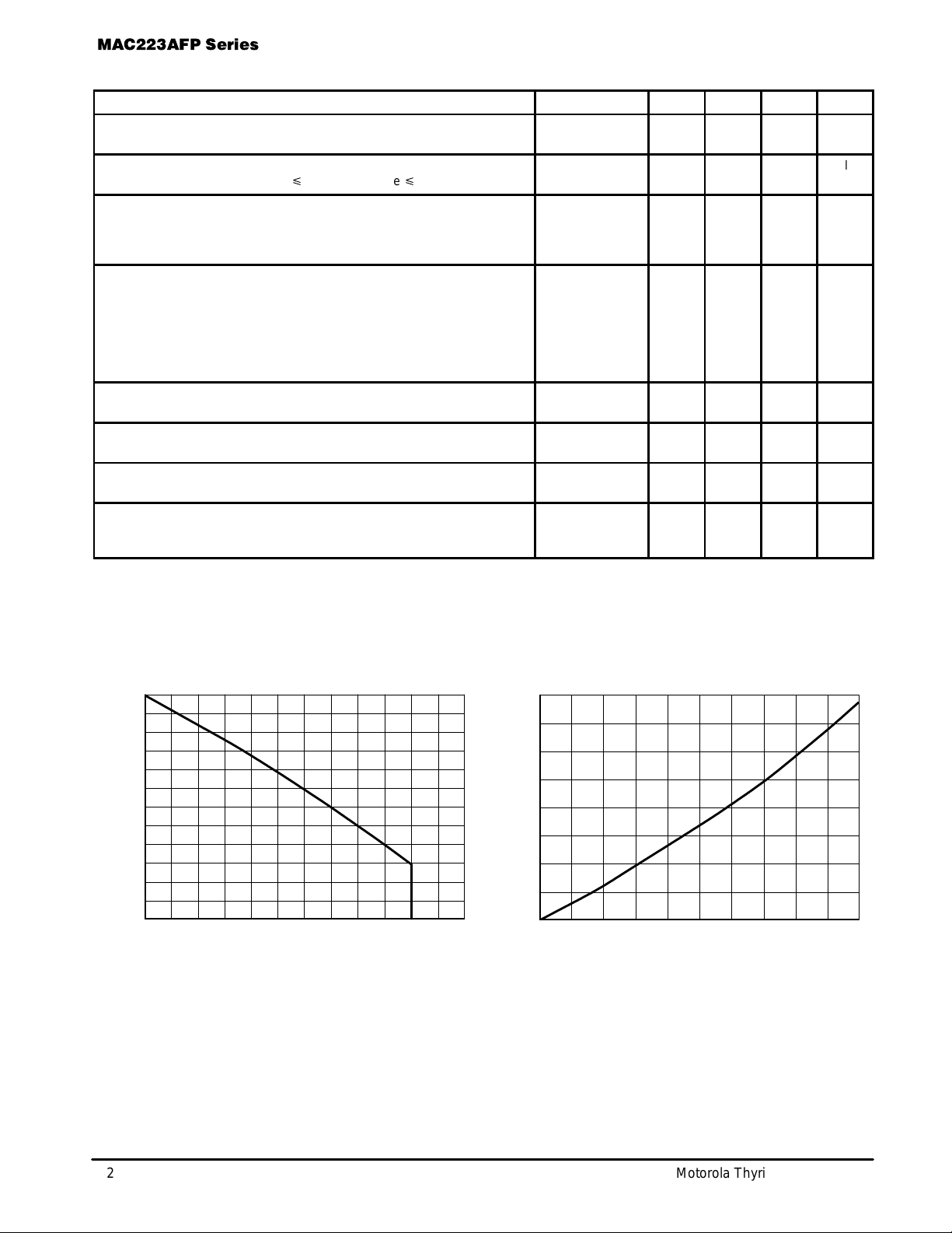
, MAXIMUM ALLOWABLE CASE TEMPERATURE ( C)
C
T
40
30
20
10
, AVERAGE POWER DISSIPATION (WATTS)
D(AV)
0
1005
I
, RMS ON–STATE CURRENT (AMPS)
T(RMS)
15
2520
P
510
I
, RMS ON–STATE CURRENT (AMPS)
T(RMS)
150
20 25
Figure 1. RMS Current Derating Figure 2. On–State Power Dissipation
2 Motorola Thyristor Device Data

TYPICAL CHARACTERISTICS
3
2
1
0.5
0.3
NORMALIZED GATE CURRENT
0.2
0.1
T
, JUNCTION TEMPERATURE (
J
Figure 3. Gate Trigger Current Figure 4. Gate Trigger Voltage
2
1
0.5
0.3
NORMALIZED HOLD CURRENT
0.2
VD = 12 V
RL = 100
W
60–60
40–40 –20 0 20
ITM = 200 mA
GATE OPEN
3
2
1
0.5
0.3
NORMALIZED GATE VOLT AGE
0.2
12010080 140
°
C)
0.1
TJ, JUNCTION TEMPERATURE (°C)
200
100
50
10
5
1
0.5
VD = 12 V
RL = 100
40–40 –20 0 20
TJ = 25°C
W
60–60
12010080 140
0.1
, INSTANTANEOUS ON–STA TE CURRENT (AMPS)
0.1
60–60
40–40 –20 0 20
TJ, JUNCTION TEMPERATURE (°C)
12010080 140
TM
i
0
1234
vTM, INSTANTANEOUS ON–STATE VOLTAGE (VOLTS)
Figure 5. Hold Current Figure 6. Typical On–State Characteristics
Motorola Thyristor Device Data
3

P ACKAGE DIMENSIONS
–Y–
SEATING
–T–
–B–
P
F
C
N
PLANE
S
E
Q
H
123
A
STYLE 3:
PIN 1. MT 1
2. MT 2
3. GATE
K
Z
L
G
3 PL
D
0.25 (0.010)
J
R
M
M
B
Y
NOTES:
1. DIMENSIONING AND TOLERANCING PER ANSI
Y14.5M, 1982.
2. CONTROLLING DIMENSION: INCH.
3. LEAD DIMENSIONS UNCONTROLLED WITHIN
DIMENSION Z.
DIM MIN MAX MIN MAX
A 0.680 0.700 17.28 17.78
B 0.388 0.408 9.86 10.36
C 0.175 0.195 4.45 4.95
D 0.025 0.040 0.64 1.01
E 0.340 0.355 8.64 9.01
F 0.140 0.150 3.56 3.81
G 0.100 BSC 2.54 BSC
H 0.110 0.155 2.80 3.93
J 0.018 0.028 0.46 0.71
K 0.500 0.550 12.70 13.97
L 0.045 0.070 1.15 1.77
N 0.049 ––– 1.25 –––
P 0.270 0.290 6.86 7.36
Q 0.480 0.500 12.20 12.70
R 0.090 0.120 2.29 3.04
S 0.105 0.115 2.67 2.92
Z 0.070 0.090 1.78 2.28
MILLIMETERSINCHES
CASE 221C-02
ISSUE B
Motorola reserves the right to make changes without further notice to any products herein. Motorola makes no warranty , representation or guarantee regarding
the suitability of its products for any particular purpose, nor does Motorola assume any liability arising out of the application or use of any product or circuit, and
specifically disclaims any and all liability, including without limitation consequential or incidental damages. “T ypical” parameters which may be provided in Motorola
data sheets and/or specifications can and do vary in different applications and actual performance may vary over time. All operating parameters, including “Typicals”
must be validated for each customer application by customer’s technical experts. Motorola does not convey any license under its patent rights nor the rights of
others. Motorola products are not designed, intended, or authorized for use as components in systems intended for surgical implant into the body, or other
applications intended to support or sustain life, or for any other application in which the failure of the Motorola product could create a situation where personal injury
or death may occur. Should Buyer purchase or use Motorola products for any such unintended or unauthorized application, Buyer shall indemnify and hold Motorola
and its officers, employees, subsidiaries, affiliates, and distributors harmless against all claims, costs, damages, and expenses, and reasonable attorney fees
arising out of, directly or indirectly, any claim of personal injury or death associated with such unintended or unauthorized use, even if such claim alleges that
Motorola was negligent regarding the design or manufacture of the part. Motorola and are registered trademarks of Motorola, Inc. Motorola, Inc. is an Equal
Opportunity/Affirmative Action Employer.
How to reach us:
USA/EUROPE /Locations Not Listed: Motorola Literature Distribution; JAPAN: Motorola Japan Ltd.; SPD, Strategic Planning Office, 141,
P.O. Box 5405, Denver, Colorado 80217. 1–303–675–2140 or 1–800–441–2447 4–32–1 Nishi–Gotanda, Shinagawa–ku, Tokyo, Japan. 81–3–5487–8488
Customer Focus Center: 1–800–521–6274
Mfax: RMFAX0@email.sps.mot.com – TOUCHTONE 1–602–244–6609 ASIA/PACIFIC: Motorola Semiconductors H.K. Ltd.; Silicon Harbour Centre,
Motorola Fax Back System – US & Canada ONLY 1–800–774–1848 2, Dai King Street, Tai Po Industrial Estate, Tai Po, N.T., Hong Kong.
HOME PAGE: http://motorola.com/sps/
4 Motorola Thyristor Device Data
– http://sps.motorola.com/mfax/ 852–26629298
◊
Mfax is a trademark of Motorola, Inc.
MAC223A6FP/D
 Loading...