

MOTOROLA MAC23A Technical data
MOTOROLA
查询MAC223A/D供应商
SEMICONDUCTOR TECHNICAL DATA
Triacs
Silicon Bidirectional Thyristors
Order this document
by MAC223A/D
MAC223A
Series
Motorola preferred devices
. . . designed primarily for full-wave ac control applications such as lighting systems,
heater controls, motor controls and power supplies; or wherever full–wave silicon–
gate–controlled devices are needed.
• Off–State Voltages to 800 Volts
TRIACs
25 AMPERES RMS
400 thru 800 VOL TS
• All Diffused and Glass Passivated Junctions for Parameter Uniformity and Stability
• Small, Rugged, Thermowatt Construction for Thermal Resistance and High Heat
Dissipation
• Gate Triggering Guaranteed in Four Modes
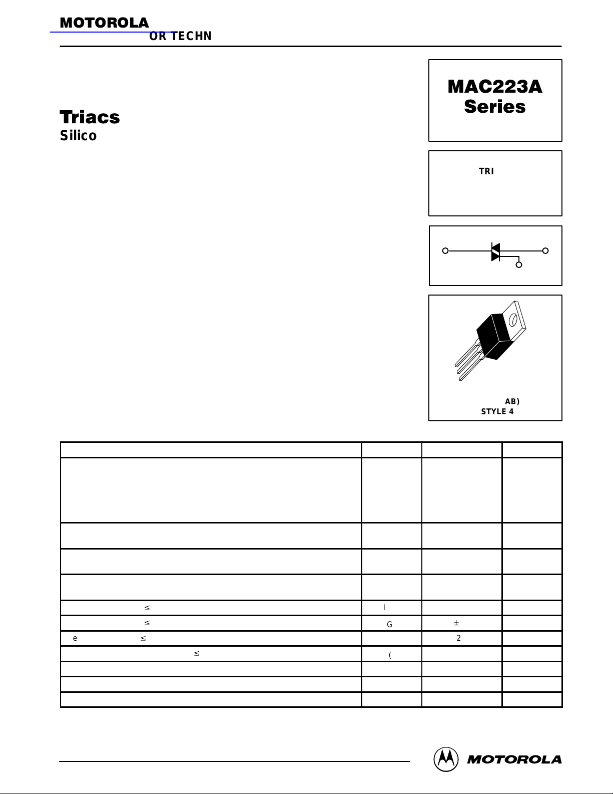
MT2
CASE 221A-07
(TO-220AB)
STYLE 4
MAXIMUM RATINGS
Peak Repetitive Off-State Voltage
(TJ = –40 to 125°C)
(1/2 Sine Wave 50 to 60 Hz, Gate Open)
On-State RMS Current (TC = 80°C)
(Full Cycle Sine Wave 50 to 60 Hz)
Peak Non-repetitive Surge Current
(One Full Cycle, 60 Hz, TC = 80°C, preceded and followed by rated current)
Circuit Fusing
(t = 8.3 ms)
Peak Gate Current (t v 2 µs) I
Peak Gate Voltage (t v 2 µs) V
Peak Gate Power (t v 2 µs) P
Average Gate Power (TC = 80°C, t v 8.3 ms) P
Operating Junction Temperature Range T
Storage Temperature Range T
Mounting Torque — 8 in. lb.
1. V
for all types can be applied on a continuous basis. Blocking voltages shall not be tested with a constant current source such that the
DRM
voltage ratings of the devices are exceeded.
(TJ = 25°C unless otherwise noted.)
Rating
(1)
MAC223A6
MAC223A8
MAC223A10
Symbol Value Unit
V
DRM
400
600
800
I
T(RMS)
I
TSM
I2t 260 A2s
GM
GM
GM
G(AV)
J
stg
25 Amps
250 Amps
2 Amps
"
10 Volts
20 Watts
0.5 Watts
–40 to 125 °C
–40 to 150 °C
G
Volts
MT1
Motorola Thyristor Device Data
Motorola, Inc. 1998
1
(
)
)
THERMAL CHARACTERISTICS
Characteristic Symbol Max Unit
Thermal Resistance, Junction to Case R
Thermal Resistance, Junction to Ambient R
ELECTRICAL CHARACTERISTICS (T
Characteristic
Peak Blocking Current
(VD = Rated V
Peak On-State Voltage
(ITM = 35 A Peak, Pulse Width v2 ms, Duty Cycle v2%)
Gate Trigger Current (Continuous dc)
(VD = 12 V, RL = 100 Ω)
MT2(+), G(+); MT2(–), G(–); MT(+), G(–)
MT2(–), G(+) “A” SUFFIX ONLY
Gate Trigger Voltage (Continuous dc)
(VD = 12 V, RL = 100 Ω)
MT2(+), G(+); MT2(–), G(–); MT(+), G(–)
MT2(–), G(+) “A” SUFFIX ONLY
(VD = Rated V
MT(+), G(+); MT2(–), G(–); MT2(+), G(–)
MT2(–), G(+) “A” SUFFIX ONLY
Holding Current
(VD = 12 V, ITM = 200 mA, Gate Open)
Gate Controlled Turn–On Time
(VD = Rated V
Critical Rate of Rise of Off-State V oltage
(VD = Rated V
Critical Rate of Rise of Commutation Voltage
(VD = Rated V
di/dt = 12.6 A/ms, Gate Unenergized, TC = 80°C)
1. Ratings apply for open gate conditions. Devices shall not be tested with a constant current source for blocking voltage such that the voltage
applied exceeds the rated blocking voltage.
(1)
)T
DRM
, TJ = 125°C, RL = 10 k)
DRM
, ITM = 35 A Peak, IG = 200 mA)
DRM
, Exponential Waveform, TC = 125°C)
DRM
, ITM = 35 A Peak, Commutating
DRM
J
TJ = 125°C
= 25°C and either polarity of MT2 to MT1 voltage unless otherwise noted.)
C
= 25°C
θJC
θJA
Symbol Min Typ Max Unit
I
DRM
V
TM
I
GT
V
GT
0.2
0.2
I
H
t
gt
dv/dt — 40 — V/µs
dv/dt(c) — 5 — V/µs
1.2 °C/W
60 °C/W
—
—
— 1.4 1.85 Volts
—
—
—
—
— 10 50 mA
— 1.5 — µs
—
—
20
30
1.1
1.3
0.4
0.4
10
50
75
2.5
—
—
2
2
µA
mA
mA
Volts
°
125
115
105
C
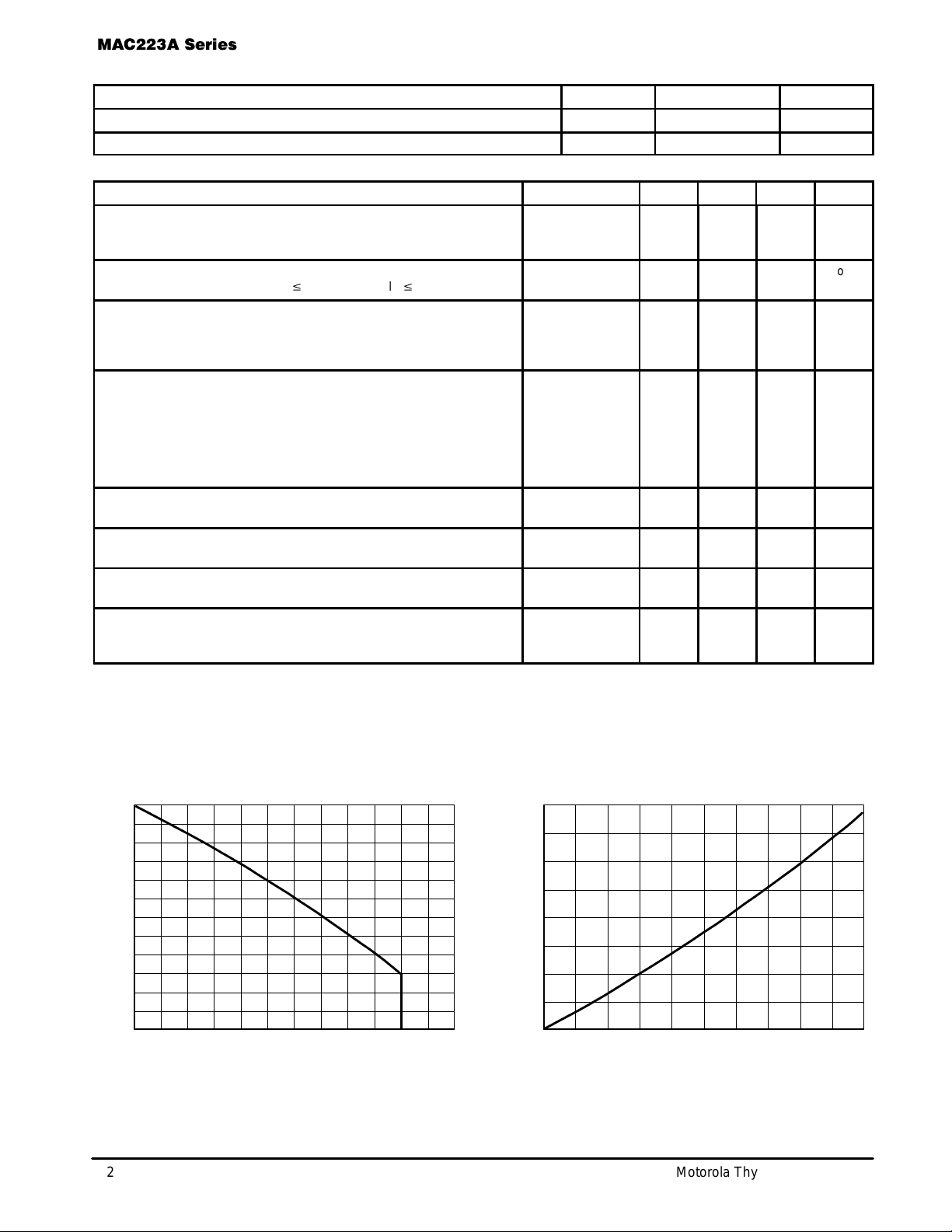
T , MAXIMUM ALLOWABLE CASE TEMPERATURE ( C)
FIGURE 1 – RMS CURRENT DERATING
95
85
75
0 5.0 10 15 20 25
, RMS ON–STATE CURRENT (AMPS)
I
RMS
T
FIGURE 2 – ON-STATE POWER DISSIPATION
40
30
20
10
, AVERAGE POWER DISSIP ATION (WATTS)
D
P
0
0 5.0 10 15 20 25
I
, RMS ON–STATE CURRENT (AMPS)
T(RMS
2 Motorola Thyristor Device Data
 Loading...