

The LM323,A are monolithic integrated circuits which supply a fixed
positive 5.0 V output with a load driving capability in excess of 3.0 A. These
three–terminal regulators employ internal current limiting, thermal shutdown,
and safe–area compensation. The A–suffix is an improved device with
superior electrical characteristics and a 2% output voltage tolerance. These
regulators are offered with a 0° to +125°C temperature range in a low cost
plastic power package.
Although designed primarily as a fixed voltage regulator, these devices
can be used with external components to obtain adjustable voltages and
currents. These devices can be used with a series pass transistor to supply
up to 15 A at 5.0 V.
• Output Current in Excess of 3.0 A
• Available with 2% Output Voltage Tolerance
• No External Components Required
• Internal Thermal Overload Protection
• Internal Short Circuit Current Limiting
• Output Transistor Safe–Area Compensation
• Thermal Regulation and Ripple Rejection Have Specified Limits
Order this document by LM323/D
3–AMPERE, 5 VOLT
POSITIVE
VOLTAGE REGULATORS
SEMICONDUCTOR
TECHNICAL DATA
T SUFFIX
PLASTIC PACKAGE
CASE 221A
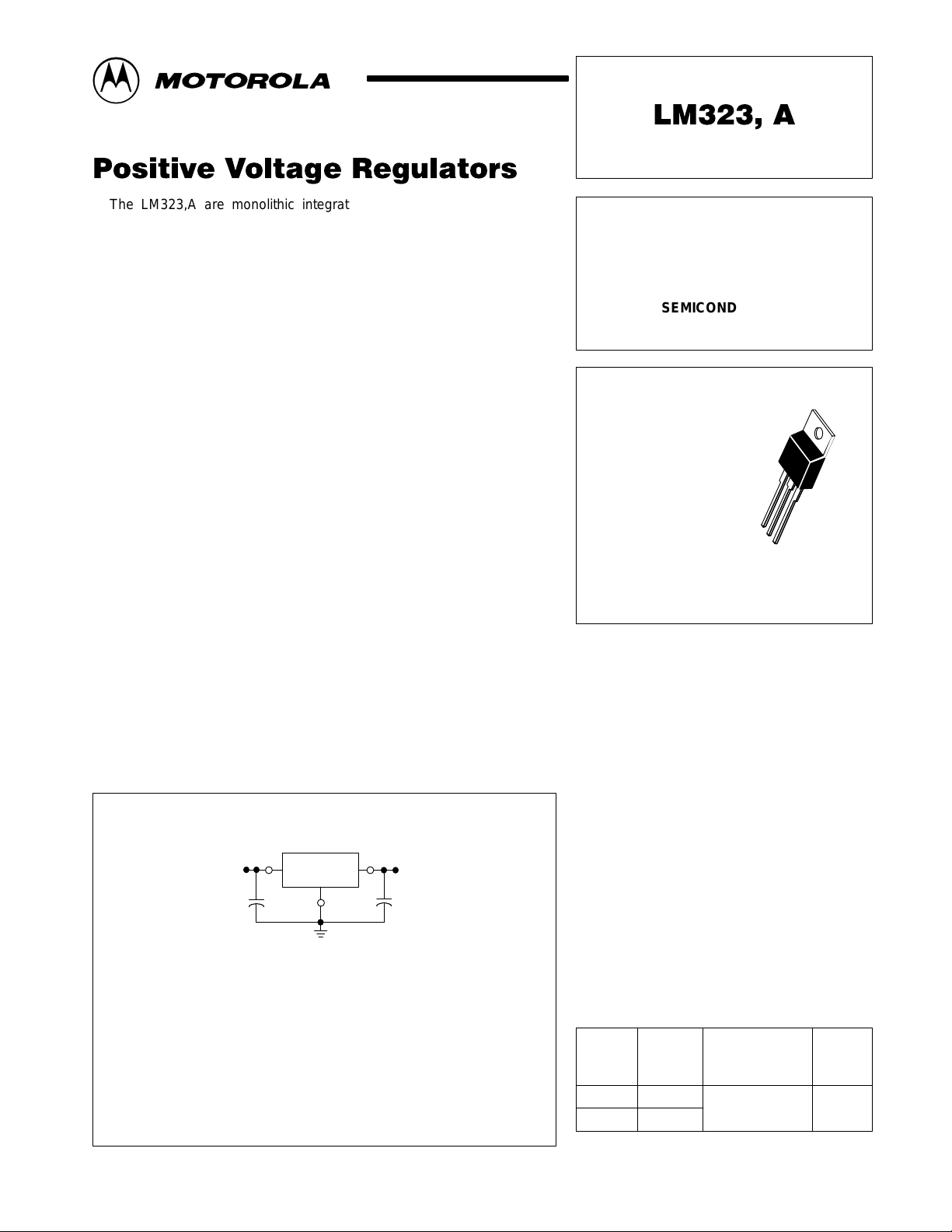
Pin 1. Input
2. Ground
3. Output
1
2
3
Simplified Application
Input
Cin*
0.33
µ
F
A common ground is required between the input and the output voltages. The input
voltage must remain typically 2.5 V above the output voltage even during the low point
on the input ripple voltage.
LM323, A
Output
CO**
Heatsink surface is connected to Pin 2.
ORDERING INFORMATION
*Cin is required if regulator is located an appreciable
*distance from power supply filter. (See Applications
*Information for details.)
**CO is not needed for stability; however, it does
**improve transient response.
MOTOROLA ANALOG IC DEVICE DATA
Output
Voltage
Device
LM323T
LM323A T
Motorola, Inc. 1996 Rev 0
Tolerance
4%
2%
Operating
Temperature
Range
TJ = 0° to +125°C
Package
Plastic
Power
1
MAXIMUM RATINGS
Rating Symbol Value Unit
Input Voltage V
Power Dissipation P
Operating Junction Temperature Range T
Storage Temperature Range T
Lead Temperature (Soldering, 10 s) T
in
D
J
stg
solder
LM323, A
20 Vdc
Internally Limited W
0 to +125 °C
–65 to +150 °C
300 °C
ELECTRICAL CHARACTERISTICS (T
J
= T
low
to T
[Note 1], unless otherwise noted.)
high
LM323A LM323
Characteristics Symbol Min Typ Max Min Typ Max Unit
Output Voltage
(Vin = 7.5 V, 0 ≤ I
≤ 3.0 A, TJ = 25°C)
out
Output Voltage
(7.5 V ≤ Vin ≤ 15 V, 0 ≤ I
P ≤ P
max
) (Note 2)
≤ 3.0 A,
out
Line Regulation
(7.5 V ≤ Vin ≤ 15 V, TJ = 25°C) (Note 3)
Load Regulation
(Vin = 7.5 V, 0 ≤ I
(Note 3)
≤ 3.0 A, TJ = 25°C)
out
Thermal Regulation
(Pulse = 10 ms, P = 20 W, TA = 25°C)
Quiescent Current
(7.5 V ≤ Vin ≤ 15 V, 0 ≤ I
out
≤ 3.0 A)
Output Noise Voltage
(10 Hz ≤ f ≤ 100 kHz, TJ = 25°C)
Ripple Rejection
(8.0 V ≤ Vin ≤ 18 V, I
f = 120 Hz, TJ = 25°C)
out
= 2.0A,
Short Circuit Current Limit
(Vin = 15 V, TJ = 25°C)
(Vin = 7.5 V, TJ = 25°C)
Reg
Reg
Reg
V
O
V
O
line
load
therm
I
B
V
N
4.9 5.0 5.1 4.8 5.0 5.2 V
4.8 5.0 5.2 4.75 5.0 5.25 V
– 1.0 15 – 1.0 25 mV
– 10 50 – 10 100 mV
– 0.001 0.01 – 0.002 0.03 %VO/W
– 3.5 10 – 3.5 20 mA
– 40 – – 40 – µV
RR 66 75 – 62 75 – dB
I
SC
–
–
4.5
5.5
–
–
–
–
4.5
5.5
–
–
Long Term Stability S – – 35 – – 35 mV
Thermal Resistance, Junction–to–Case (Note 4) R
NOTES: 1.T
to T
low
2.Although power dissipation is internally limited, specifications apply only for P ≤ P
3.Load and line regulation are specified at constant junction temperature. Pulse testing is required with a pulse width ≤ 1.0 ms and a duty cycle ≤ 5%.
4.Without a heatsink, the thermal resistance (R
2.0°C/W, depending on the ef ficiency of the heatsink.
= 0° to +125°C
high
θJA
ΘJC
is 65°C/W). With a heatsink, the effective thermal resistance can approach the specified values of
– 2.0 – – 2.0 – °C/W
= 25 W.
max
rms
A
2
MOTOROLA ANALOG IC DEVICE DATA
LM323, A
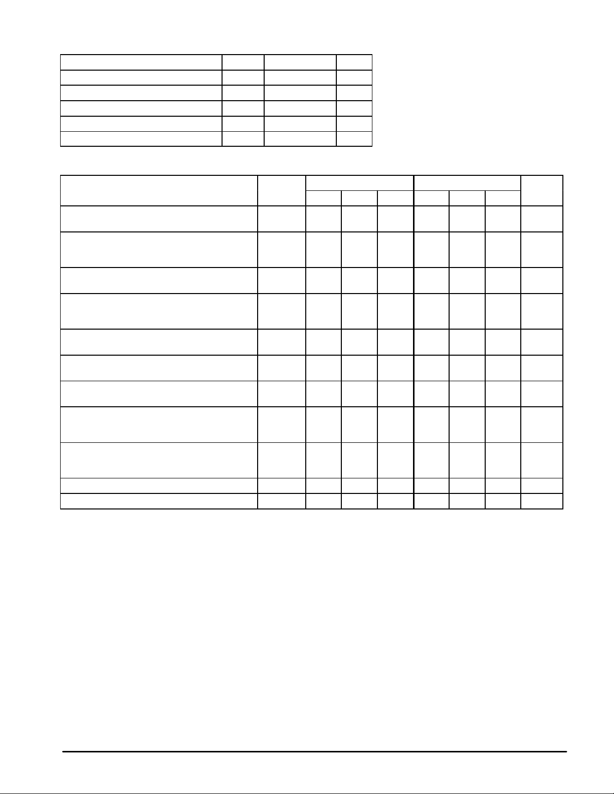
Representative Schematic Diagram
Q1
Q4
Q5
Q6 Q7
1.0k
300
Q3 10k
Q12
Q11
6.0k
Q8
2.0k
Q13
Q14
Q2
Q10
1.0k
2.6k
3.9k
Q9
6.0k
3.0k
5.6k
40pF
Q17 Q18
Q15
2.8k
VOLTAGE REGULATOR PERFORMANCE
The performance of a voltage regulator is specified by its
immunity to changes in load, input voltage, power dissipation,
and temperature. Line and load regulation are tested with a
pulse of short duration (< 100 µs) and are strictly a function of
electrical gain. However, pulse widths of longer duration
(> 1.0 ms) are sufficient to affect temperature gradients
across the die. These temperature gradients can cause a
change in the output voltage, in addition to changes by line
and load regulation. Longer pulse widths and thermal
gradients make it desirable to specify thermal regulation.
Thermal regulation is defined as the change in output
voltage caused by a change in dissipated power for a
specified time, and is expressed as a percentage output
voltage change per watt. The change in dissipated power can
2
210
Q24
Q21
100
200
Q25
Q26
13
200
Q20
Q16
Q19
1.0k
10pF
Q23
7.2k
Q22
6.7V
50520
16k
300
be caused by a change in either input voltage or the load
current. Thermal regulation is a function of IC layout and die
attach techniques, and usually occurs within 10 ms of a
change in power dissipation. After 10 ms, additional changes
in the output voltage are due to the temperature coefficient of
the device.
Figure 1 shows the line and thermal regulation response of
a typical LM323A to a 20 W input pulse. The variation of the
output voltage due to line regulation is labeled À and the
thermal regulation component is labeled Á. Figure 2 shows
the load and thermal regulation response of a typical LM323A
to a 20 W load pulse. The output voltage variation due to load
regulation is labeled À and the thermal regulation component
is labeled Á.
Input
Q27
0.12
Output
840
1.7k
Gnd
Figure 1. Line and Thermal Regulation Figure 2. Load and Thermal Regulation
2
, OUTPUT
out
V
∆
VOLTAGE DEVIATION (V)
, INPUT
in
V
(2.0 mV/DIV)
18 V
8.0 V
VOLTAGE (V)
V
= 5.0 V
out
Vin = 8.0 V
I
= 2.0 A
out
→
18 V → 8.0 V
1
t, TIME (2.0 ms/DIV)
1
= Reg
2
MOTOROLA ANALOG IC DEVICE DATA
= 2.4 mV
line
= 0.0015% VO/W
therm
2
, OUTPUT
out
V
∆
(2.0 mV/DIV)
, OUTPUT
out
I
CURRENT (A) VOLTAGE DEVIA TION (V)
2
2.0
0
V
= 5.0 V
out
Vin = 15 V
I
= 0 A
out
→
2.0 A → 0 A
2
1
t, TIME (2.0 ms/DIV)
= Reg
1
line
= Reg
2
therm
= 5.4 mV
= 0.0015% VO/W= Reg
3
5.1
5.0
LM323, A
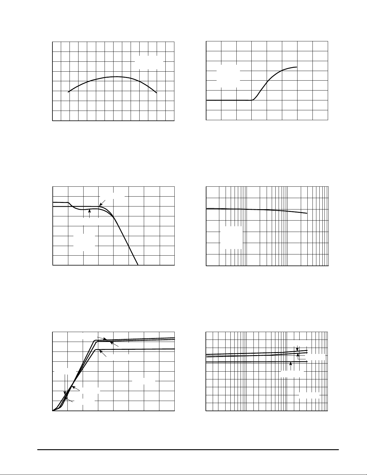
Figure 3. T emperature Stability Figure 4. Output Impedance
10
Ω
Vin = 10 V
I
= 100 mA
out
10
10
–1
–2
Vin = 7.5 V
I
= 1.0 A
out
CO = 0
°
C
TJ = 25
, OUTPUT VOL TAGE (Vdc)
out
V
4.9
–90 –50 –10 30 70 110 150
TJ, JUNCTION TEMPERATURE (
°
190
C)
–3
, OUTPUT IMPEDANCE ( )
10
O
Z
–4
10
1.0 10 100 1.0 k 10 k 100 k 1.0 M 10 M 100 M
f, FREQUENCY (Hz)
Figure 5. Ripple Rejection versus Frequency Figure 6. Ripple Rejection versus Output Current
100
I
= 50 mA
out
80
I
= 3.0 A
60
40
RR, RIPPLE REJECTION (dB)
20
1.0 10 100 1.0 k 10 k 100 k 1.0 M 10 M 100 M
out
Vin = 10 V
CO = 0
°
C
TJ = 25
f, FREQUENCY (Hz)
100
80
60
RR, RIPPLE REJECTION (dB)
40
30
0.01 0.1 1.0 10
Vin = 10 V
CO = 0
f = 120 Hz
°
C
TJ = 25
I
, OUTPUT CURRENT (A)
out
Figure 7. Quiescent Current versus
Input Voltage
4.0
3.0
2.0
TJ = 150
1.0
, QUIESCENT CURRENT (mA)
B
I
0
0 5.0 10 15 20
°
C
TJ = 25
TJ = 55°C
TJ = 150
TJ = 55°C
°
C
Vin, INPUT VOLTAGE (Vdc)
TJ = 25
°
C
°
I
C
out
= 2.0 A
4
Figure 8. Quiescent Current versus
Output Current
5.0
4.0
3.0
2.0
, QUIESCENT CURRENT (mA)
1.0
B
I
0
0.01 0.1 1.0 10
I
, OUTPUT CURRENT (A)
out
TJ = –55°C
TJ = 150
TJ = 25
°
C
Vin = 10 V
MOTOROLA ANALOG IC DEVICE DATA
°
C
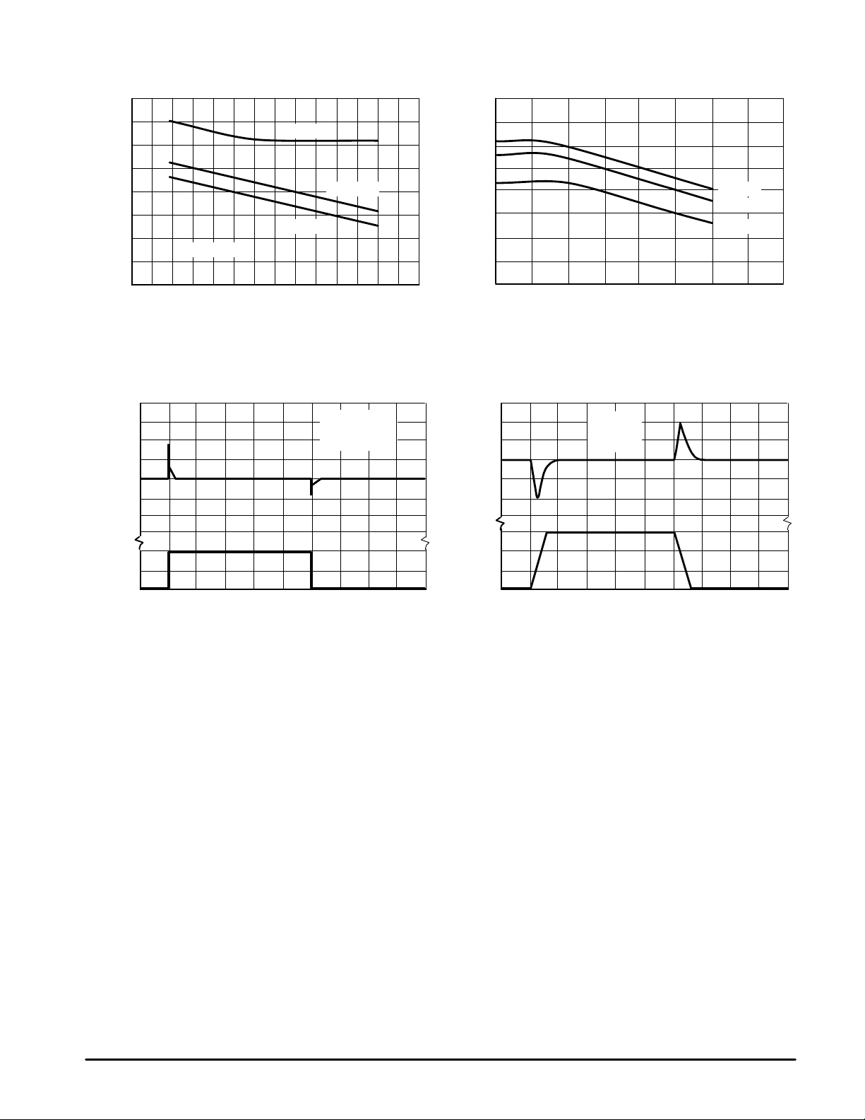
Figure 9. Dropout Voltage Figure 10. Short Circuit Current
2.5
I
= 3.0 A
I
out
out
= 0.5 A
I
out
°
C)
= 1.0 A
2.0
1.5
, INPUT TO OUTPUT
out
–V
1.0
in
V
VOLTAGE DIFFERENTIAL (Vdc)
0.5
–90 –50 –10 30 70 110 150 190
∆
V
= 50 mV
out
TJ, JUNCTION TEMPERATURE (
Figure 11. Line Transient Response Figure 12. Load Transient Response
0.8
I
= 150 mA
0.6
0.4
0.2
, OUTPUT VOL TAGE
DEVIATION (V)
0
out
V
–0.2
∆
–0.4
–0.6
1.0
0.5
0
CHANGE (V)
, INPUT VOLTAGE
in
V
∆
010203040
t, TIME (
out
CO = 0
°
TJ = 25
µ
s)
C
LM323, A
SC
I , SHORT CIRCUIT CURRENT AT
, OUTPUT VOL TAGE
out
V
∆
, OUTPUT
out
I
8.0
6.0
4.0
ZERO VOLTS (A)
2.0
0
5.0 10 15 20 25
Vin, INPUT VOLTAGE (Vdc)
0.3
0.2
0.1
0
–0.1
DEVIATION (V)
–0.2
–0.3
1.5
1.0
0.5
CURRENT (A)
0
010203040
Vin = 10 V
CO = 0
°
C
TJ = 25
t, TIME (
µ
s)
TJ = 0°C
TJ = 25
TJ = 125
°
C
°
C
APPLICATIONS INFORMATION
Design Considerations
The LM323,A series of fixed voltage regulators are
designed with Thermal Overload Protection that shuts down
the circuit when subjected to an excessive power overload
condition, Internal Short Circuit Protection that limits the
maximum current the circuit will pass, and Output Transistor
Safe–Area Compensation that reduces the output short
circuit current as the voltage across the pass transistor is
increased.
In many low current applications, compensation
capacitors are not required. However, it is recommended that
the regulator input be bypassed with a capacitor if the
MOTOROLA ANALOG IC DEVICE DATA
regulator is connected to the power supply filter with long wire
lengths, or if the output load capacitance is large. An input
bypass capacitor should be selected to provide good
high–frequency characteristics to insure stable operation
under all load conditions. A 0.33 µF or larger tantalum, mylar,
or other capacitor having low internal impedance at high
frequencies should be chosen. The bypass capacitor should
be mounted with the shortest possible leads directly across
the regulator’s input terminals. Normally good construction
techniques should be used to minimize ground loops and
lead resistance drops since the regulator has no external
sense lead.
5
LM323, A
Figure 13. Current Regulator Figure 14. Adjustable Output Regulator
Input
0.33
µ
F
The LM323,A regulator can also be used as a current source when
connected as above. Resistor R determines the current as follows:
∆
IB ^ 0.7 mA over line, load and temperature changes
^
3.5 mA
IB
For example, a 2.0 A current source would require R to be a 2.5
15 W resistor and the output voltage compliance would be the input
voltage less 7.5 V.
LM323, A
5.0 V
IO =
R
Constant
Current to
Grounded Load
I
O
+ I
B
R
Ω
,
Figure 15. Current Boost Regulator
2N4398 or Equiv
Input
The addition of an operational amplifier allows adjustment to higher or
intermediate values while retaining regulation characteristics. The
minimum voltage obtainable with this arrangement is 3.0 V greater
than the regulator voltage.
LM323, A
0.33µF
1.0k
VO, 8.0 V to 20 V
7
6
MC1741
4
Vin – VO ≥ 2.5 V
2
–
3
+
Output
10k
Figure 16. Current Boost with
Short Circuit Protection
2N4398
Input R
sc
or Equiv.
0.1µF
R
1.0µF
The LM323, A series can be current boosted with a PNP transistor. The
2N4398 provides current to 15 A. Resistor R in conjuction with the V
the PNP determines when the pass transistor begins conducting; this
circuit is not short circuit proof. Input–output differential voltage
minimum is increased by the VBE of the pass transistor.
LM323, A
0.1
Output
µ
F
BE
of
MJ2955
or Equiv.
R
µ
F
1.0
The circuit of Figure 16 can be modified to provide supply protection
against short circuits by adding a short circuit sense resistor, RSC, and
an additional PNP transistor. The current sensing PNP must be able to
handle the short circuit current of the three–terminal regulator.
Therefore, an 8.0 A power transistor is specified.
LM323, A
Output
6
MOTOROLA ANALOG IC DEVICE DATA
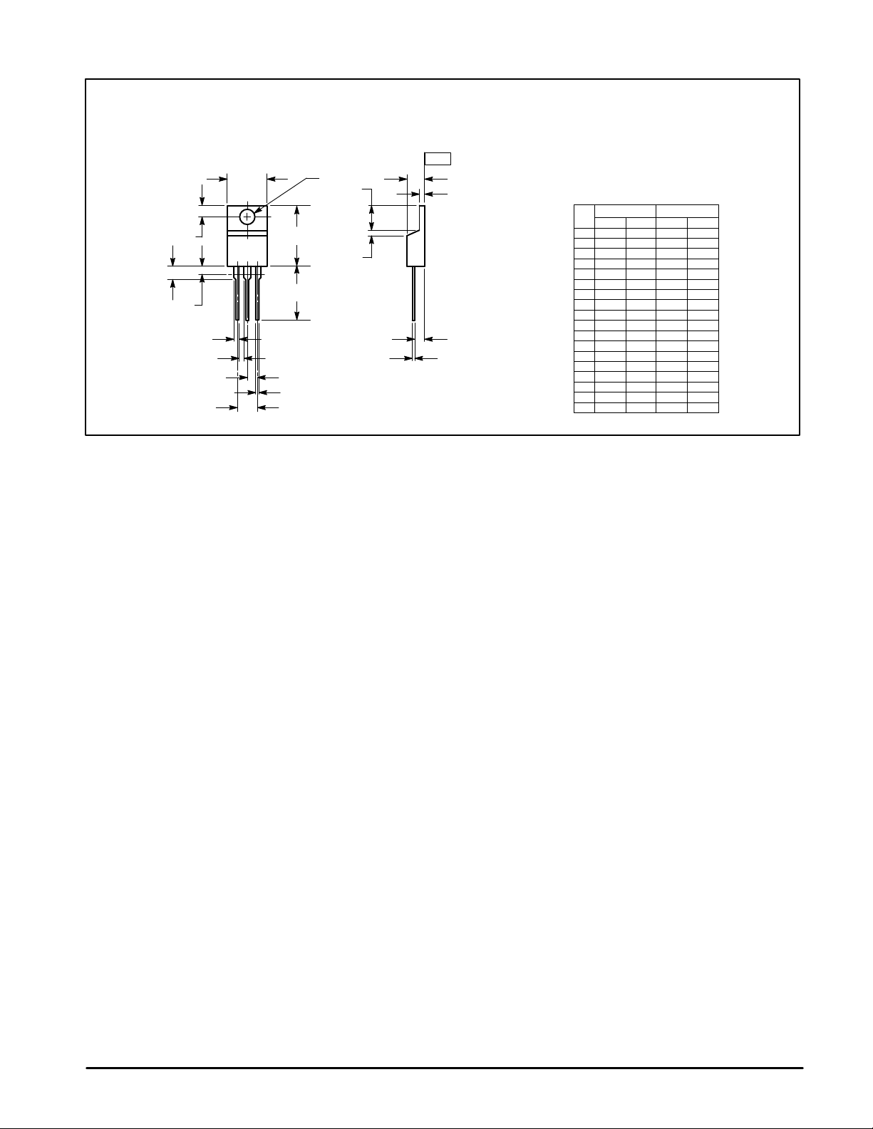
LM323, A
OUTLINE DIMENSIONS
T SUFFIX
PLASTIC PACKAGE
CASE 221A–06
ISSUE Y
SEATING
–T–
PLANE
B
4
Q
123
F
T
A
U
C
S
H
K
Z
L
V
R
J
G
D
N
NOTES:
1. DIMENSIONING AND TOLERANCING PER ANSI
Y14.5M, 1982.
2. CONTROLLING DIMENSION: INCH.
3. DIMENSION Z DEFINES A ZONE WHERE ALL
BODY AND LEAD IRREGULARITIES ARE
ALLOWED.
DIM MIN MAX MIN MAX
A 0.570 0.620 14.48 15.75
B 0.380 0.405 9.66 10.28
C 0.160 0.190 4.07 4.82
D 0.025 0.035 0.64 0.88
F 0.142 0.147 3.61 3.73
G 0.095 0.105 2.42 2.66
H 0.110 0.155 2.80 3.93
J 0.018 0.025 0.46 0.64
K 0.500 0.562 12.70 14.27
L 0.045 0.060 1.15 1.52
N 0.190 0.210 4.83 5.33
Q 0.100 0.120 2.54 3.04
R 0.080 0.110 2.04 2.79
S 0.045 0.055 1.15 1.39
T 0.235 0.255 5.97 6.47
U 0.000 0.050 0.00 1.27
V 0.045 ––– 1.15 –––
Z ––– 0.080 ––– 2.04
MILLIMETERSINCHES
MOTOROLA ANALOG IC DEVICE DATA
7

LM323, A
Motorola reserves the right to make changes without further notice to any products herein. Motorola makes no warranty , representation or guarantee regarding
the suitability of its products for any particular purpose, nor does Motorola assume any liability arising out of the application or use of any product or circuit, and
specifically disclaims any and all liability, including without limitation consequential or incidental damages. “T ypical” parameters which may be provided in Motorola
data sheets and/or specifications can and do vary in different applications and actual performance may vary over time. All operating parameters, including “Typicals”
must be validated for each customer application by customer’s technical experts. Motorola does not convey any license under its patent rights nor the rights of
others. Motorola products are not designed, intended, or authorized for use as components in systems intended for surgical implant into the body, or other
applications intended to support or sustain life, or for any other application in which the failure of the Motorola product could create a situation where personal injury
or death may occur. Should Buyer purchase or use Motorola products for any such unintended or unauthorized application, Buyer shall indemnify and hold Motorola
and its officers, employees, subsidiaries, affiliates, and distributors harmless against all claims, costs, damages, and expenses, and reasonable attorney fees
arising out of, directly or indirectly, any claim of personal injury or death associated with such unintended or unauthorized use, even if such claim alleges that Motorola
was negligent regarding the design or manufacture of the part. Motorola and are registered trademarks of Motorola, Inc. Motorola, Inc. is an Equal
Opportunity/Affirmative Action Employer.
How to reach us:
USA/EUROPE/Locations Not Listed: Motorola Literature Distribution; JAPAN: Nippon Motorola Ltd.; Tatsumi–SPD–JLDC, 6F Seibu–Butsuryu–Center,
P.O. Box 20912; Phoenix, Arizona 85036. 1–800–441–2447 or 602–303–5454 3–14–2 Tatsumi Koto–Ku, Tokyo 135, Japan. 03–81–3521–8315
MFAX: RMF AX0@email.sps.mot.com – TOUCHT ONE 602–244–6609 ASIA/PACIFIC: Motorola Semiconductors H.K. Ltd.; 8B Tai Ping Industrial Park,
INTERNET: http://Design–NET.com 51 Ting Ko k Road, Tai Po, N.T ., Hong Kong. 852–26629298
8
◊
MOTOROLA ANALOG IC DEVICE DATA
LM323/D
*LM323/D*
 Loading...