

Order this document by LM317L/D
Order this document by LM317L/D
The LM317L is an adjustable 3–terminal positive voltage regulator
capable of supplying in excess of 100 mA over an output voltage range of
1.2 V to 37 V. This voltage regulator is exceptionally easy to use and
requires only two external resistors to set the output voltage. Further, it
employs internal current limiting, thermal shutdown and safe area
compensation, making them essentially blow–out proof.
The LM317L serves a wide variety of applications including local, on card
regulation. This device can also be used to make a programmable output
regulator, or by connecting a fixed resistor between the adjustment and
output, the LM317L can be used as a precision current regulator.
• Output Current in Excess of 100 mA
• Output Adjustable Between 1.2 V and 37 V
• Internal Thermal Overload Protection
• Internal Short Circuit Current Limiting
• Output Transistor Safe–Area Compensation
• Floating Operation for High Voltage Applications
• Standard 3–Lead Transistor Package
• Eliminates Stocking Many Fixed Voltages
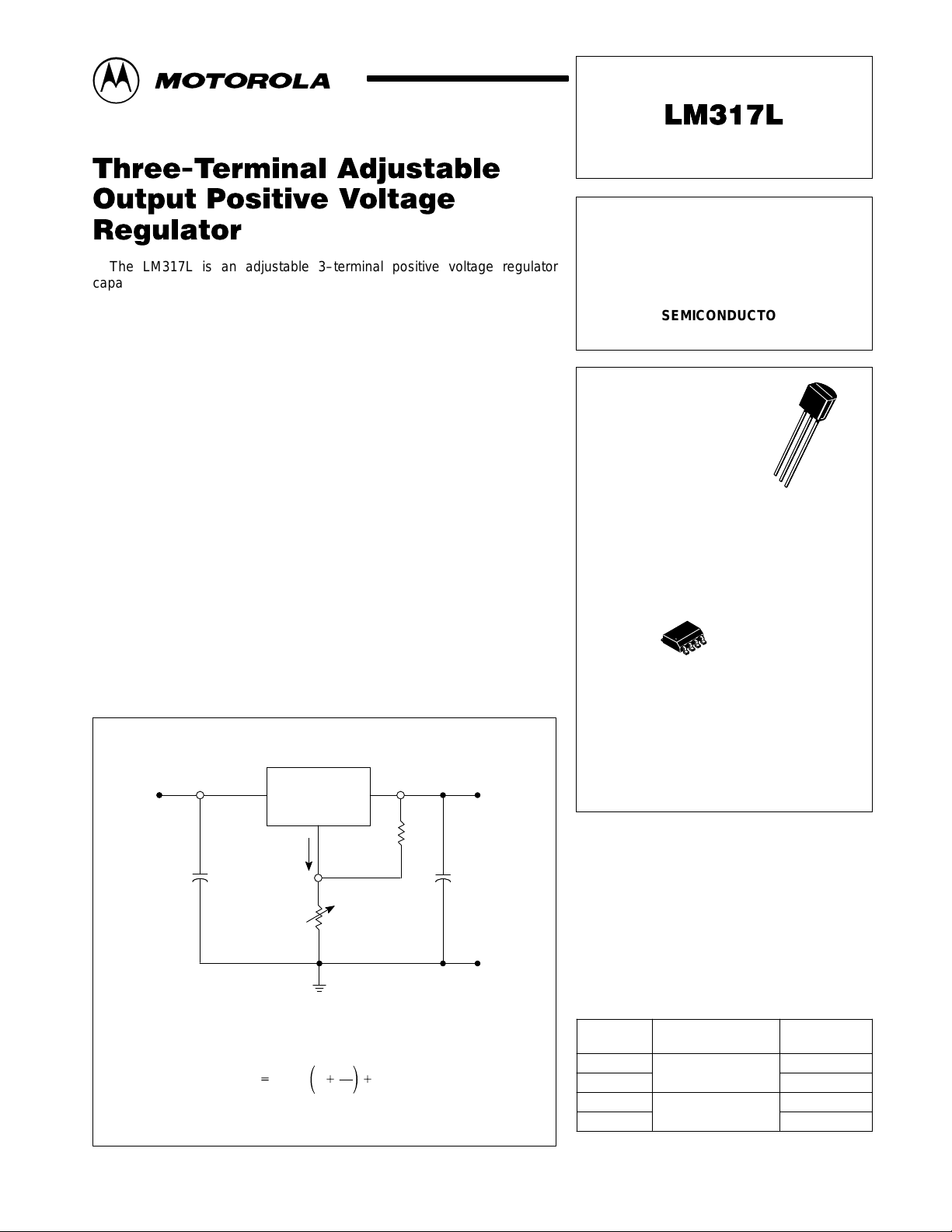
Simplified Application
V
in
LM317L
V
out
LOW CURRENT
LOW CURRENT
THREE–TERMINAL
THREE–TERMINAL
ADJUSTABLE POSITIVE
ADJUSTABLE POSITIVE
VOLTAGE REGULATOR
VOLTAGE REGULATOR
SEMICONDUCTOR
SEMICONDUCTOR
TECHNICAL DATA
TECHNICAL DATA
Z SUFFIX
Z SUFFIX
PLASTIC PACKAGE
PLASTIC PACKAGE
CASE 29
CASE 29
Pin 1. Adjust
Pin 1. Adjust
2. V
2. V
out
out
3. V
3. V
in
in
D SUFFIX
D SUFFIX
PLASTIC PACKAGE
PLASTIC PACKAGE
CASE 751
CASE 751
(SOP–8*)
(SOP–8*)
8
8
1
1
* SOP–8 is an internally modified SO–8 pack-
* SOP–8 is an internally modified SO–8 pack-
age. Pins 2, 3, 6 and 7 are electrically common
age. Pins 2, 3, 6 and 7 are electrically common
to the die attach flag. This internal lead frame
to the die attach flag. This internal lead frame
modification decreases package thermal resis-
modification decreases package thermal resistance and increases power dissipation capabili-
tance and increases power dissipation capability when appropriately mounted on a printed cir-
ty when appropriately mounted on a printed circuit board. SOP–8 conforms to all external di-
cuit board. SOP–8 conforms to all external dimensions of the standard SO–8 package.
mensions of the standard SO–8 package.
1
1
2
2
3
3
Pin 1. V
Pin 1. V
2. V
2. V
3. V
3. V
4. Adjust
4. Adjust
5. N.C.
5. N.C.
6. V
6. V
7. V
7. V
8. N.C.
8. N.C.
in
in
out
out
out
out
out
out
out
out
I
Adj
Cin*
0.1
µ
F
* Cin is required if regulator is located an appreciable
** distance from power supply filter.
** CO is not needed for stability, however,
** it does improve transient response.
V
+
1.25 Vǒ1
out
Since I
is controlled to less than 100
Adj
associated with this term is negligible in most applications.
Adjust
R
2
R
)
R
2
1
MOTOROLA ANALOG IC DEVICE DATA
Ǔ
)
I
AdjR2
R
1
240
µ
A, the error
+
CO**
1.0
µ
F
ORDERING INFORMATION
ORDERING INFORMATION
Operating
Operating
Temperature Range
Device Package
Device Package
LM317LD
LM317LD
LM317LZ
LM317LZ
LM317LBD SOP–8
LM317LBD SOP–8
LM317LBZ
LM317LBZ
Motorola, Inc. 1996 Rev 1
Temperature Range
TJ = 0° to +125°C
TJ = 0° to +125°C
TJ = –40° to +125°C
TJ = –40° to +125°C
SOP–8
SOP–8
Plastic
Plastic
Plastic
Plastic
1
MAXIMUM RATINGS
Rating Symbol Value Unit
Input–Output V oltage Differential VI–V
Power Dissipation P
Operating Junction Temperature Range T
Storage Temperature Range T
D
J
stg
O
LM317L
40 Vdc
Internally Limited W
–40 to +125 °C
–65 to +150 °C
ELECTRICAL CHARACTERISTICS (V
= 5.0 V; IO = 40 mA; TJ = T
I–VO
low
to T
high
[Note 1]; I
max
and P
max
[Note 2];
unless otherwise noted.)
LM317L, LB
Characteristics Figure Symbol Min Typ Max Unit
Line Regulation (Note 3)
TA = 25°C, 3.0 V ≤ VI – VO ≤ 40 V
Load Regulation (Note 3), TA = 25°C
10 mA ≤ IO ≤ I
VO ≤ 5.0 V
max
– LM317L
VO ≥ 5.0 V
Adjustment Pin Current 3 I
Adjustment Pin Current Change
2.5 V ≤ VI – VO ≤ 40 V, PD ≤ P
10 mA ≤ IO ≤ I
max
– LM317L
max
Reference Voltage
3.0 V ≤ VI – VO ≤ 40 V, PD ≤ P
10 mA ≤ IO ≤ I
max
– LM317L
max
Line Regulation (Note 3)
3.0 V ≤ VI – VO ≤ 40 V
Load Regulation (Note 3)
10 mA ≤ IO ≤ I
VO ≤ 5.0 V
max
– LM317L
VO ≥ 5.0 V
Temperature Stability (T
low
≤ TJ ≤ T
) 3 T
high
Minimum Load Current to Maintain Regulation (VI – VO = 40 V) 3 I
Maximum Output Current
VI – VO ≤ 6.25 V, PD ≤ P
VI – VO ≤ 40 V, PD ≤ P
RMS Noise, % of V
TA = 25°C, 10 Hz ≤ f ≤ 10 kHz
O
, Z Package
max
, TA = 25°C, Z Package
max
Ripple Rejection (Note 4)
VO = 1.2 V, f = 120 Hz
C
= 10 µF, VO = 10.0 V
Adj
Long Term Stability, TJ = T
TA = 25°C for Endpoint Measurements
high
(Note 5)
Thermal Resistance, Junction–to–Case
Z Package
Thermal Resistance, Junction–to–Air
Z Package
NOTES: 1. T
to T
low
2.I
max
3.Load and line regulation are specified at constant junction temperature. Changes in VO due to heating effects must be taken into account separately.
Pulse testing with low duty cycle is used.
4.C
Adj
5.Since Long–T erm Stability cannot be measured on each device before shipment, this specification is an engineering estimate of average stability
from lot to lot.
= 0° to +125°C for LM317L –40° to +125°C for LM317LB
high
= 100 mA P
, when used, is connected between the adjustment pin and ground.
= 625 mW
max
1 Reg
2 Reg
1, 2 ∆I
3 V
1 Reg
2 Reg
3 I
line
load
Adj
Adj
ref
line
load
S
Lmin
max
– 0.01 0.04 %/V
–
–
5.0
0.1
– 50 100 µA
– 0.2 5.0 µA
1.20 1.25 1.30 V
– 0.02 0.07 %/V
–
–
20
0.3
– 0.7 – % V
– 3.5 10 mA
100
–
200
20
N – 0.003 – % V
4 RR
60
–
80
80
3 S – 0.3 1.0 %/1.0 k
R
R
θJC
θJA
– 83 – °C/W
– 160 – °C/W
25
0.5mV% V
70
1.5mV% V
mA
–
–
dB
–
–
Hrs.
O
O
O
O
2
MOTOROLA ANALOG IC DEVICE DATA
LM317L
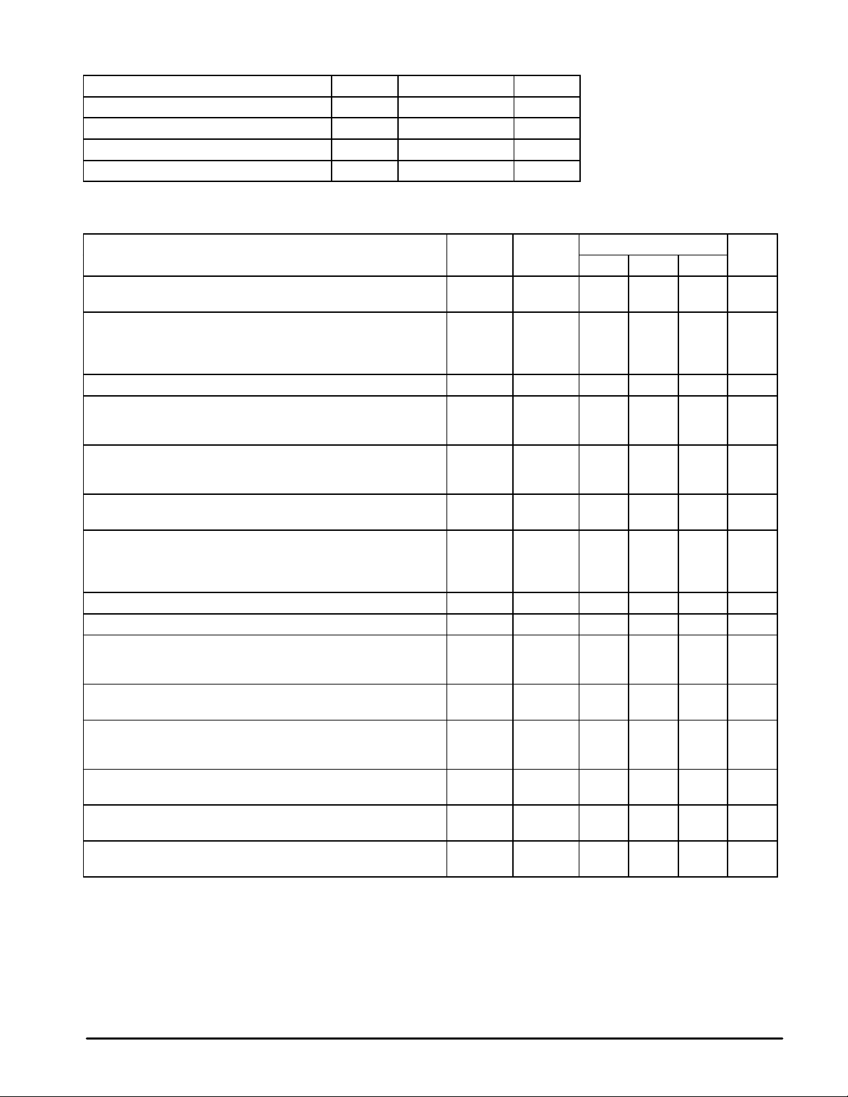
Representative Schematic Diagram
V
in
300 300 300 3.0k 30
0
350
70
6.8V
6.8V
18k
200
6.3V
*
8.67k
130
5.1k
k
180 180
V
CC
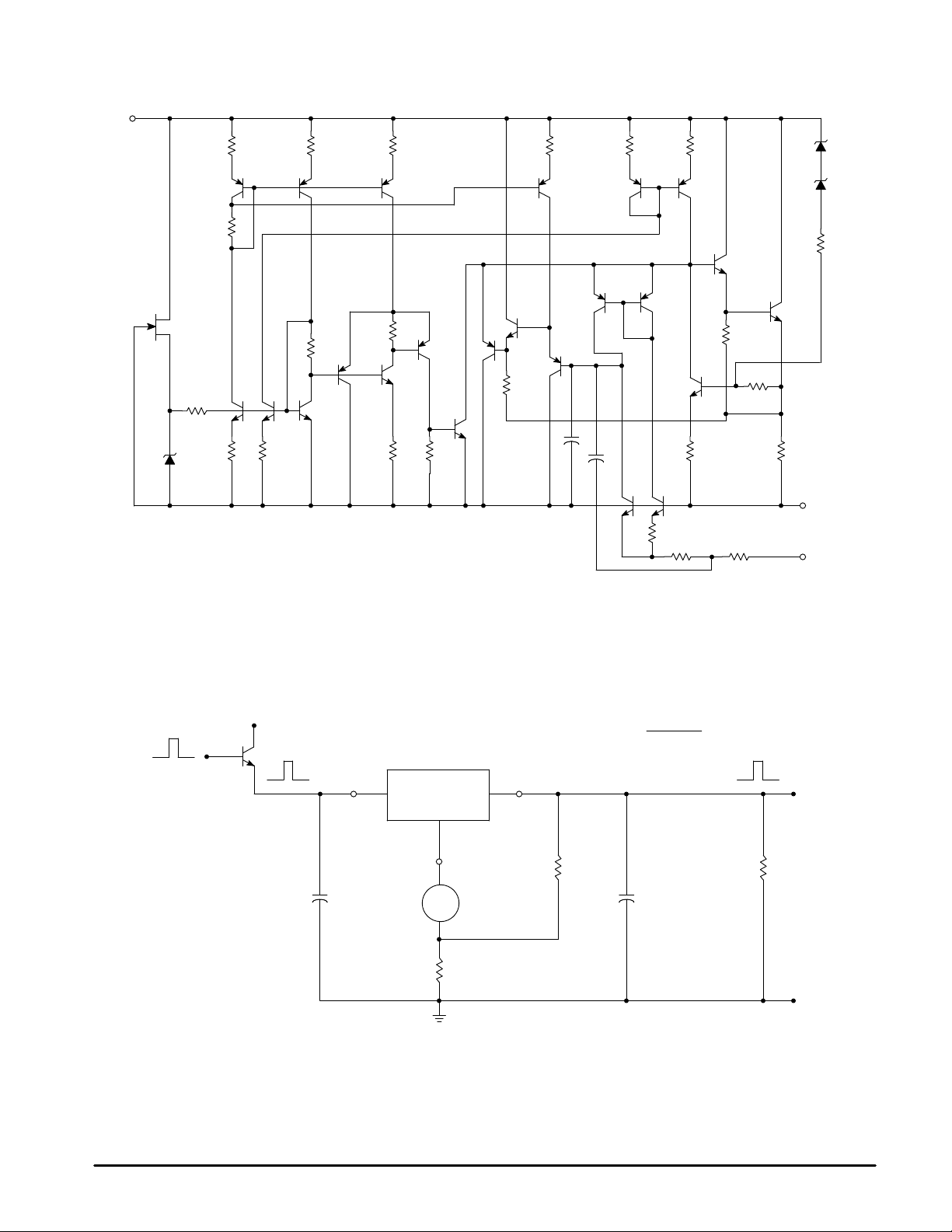
Figure 1. Line Regulation and ∆I
V
IH
VILV
2.0k 6.0k
in
LM317L
10
pF
10
pF
/Line T est Circuit
Adj
Line Regulation (%/V) =
V
out
2.4k
12.8k
VOH – V
V
OL
OL
x 100
500
5
0
40
0
2.560
V
out
Adjust
V
OH
V
OL
C
0.1µF
in
* Pulse Testing Required:
1% Duty Cycle is suggested.
MOTOROLA ANALOG IC DEVICE DATA
I
Adj
Adjust
R2
1
%
240
R
1
1%
+
1
µ
O
FC
R
L
3
LM317L
Vin*V
C
in
* Pulse Testing Required:
1% Duty Cycle is suggested.
0.1
in
µ
F
V
in
Figure 2. Load Regulation and ∆I
Load Regulation (mV) = VO (min Load) –VO (max Load)
VO (min Load) – VO (max Load)
I
L
240
1%
CO1.0
LM317L
Adjust
I
Adj
R
1%
Load Regulation (% VO) =
V
out
R
2
1
Figure 3. Standard T est Circuit
V
LM317L
out
/Load Test Circuit
Adj
VO (min Load)
+
µ
F
I
X
100
R
L
(max Load)
*
L
VO (min Load)
VO (max Load)
R
L
(min Load)
V
Pulse Testing Required:
1% Duty Cycle is suggested.
14.30V
4.30V
f = 120 Hz
C
I
in
Cin0.1
0.1
Adjust
I
µ
F
Adj
I
SET
R
1%
2
To Calculate R2:
V
= I
out
Assume I
R
1
SET R2
SET
240
1%
+ 1.250 V
= 5.25 mA
V
ref
+
1
µ
O
FC
R
L
V
O
Figure 4. Ripple Rejection T est Circuit
V
in
µ
F
LM317L
Adjust
V
out
240
R
1
1%
D1 *
1N4002
C
+
1µF
O
V
= 1.25 V
out
R
L
V
O
*D1 Discharges C
4
if Output is Shorted to Ground.
Adj
1.65K
R
2
1%
+
µ
F
10
**
**C
provides an AC ground to the adjust pin.
Adj
MOTOROLA ANALOG IC DEVICE DATA

LM317L
Figure 5. Load Regulation Figure 6. Ripple Rejection
0.4
0.2
0
–0.2
–0.4
–0.6
, OUTPUT VOLTAGE CHANGE (%)
out
–0.8
V
∆
–1.0
–50 –25 0 25 50 75 100 125 150
TJ, JUNCTION TEMPERATURE (°C)
Vin = 45 V
V
= 5.0 V
out
IL = 5.0 mA to 40 mA
Vin = 10 V
V
= 5.0 V
out
IL = 5.0 mA to 100 mA
Figure 7. Current Limit Figure 8. Dropout Voltage
0.50
TJ = 25°C
0.40
0.30
0.20
, OUTPUT CURRENT (A)
O
I
0.10
0
0 1020304050
TJ = 150
°
C
V
, INPUT–OUTPUT VOLTAGE DIFFERENTIAL (V)
in–Vout
80
70
IL = 40 mA
f = 120 Hz
V
= 10 V
60
RR, RIPPLE REJECTION (dB)
50
2.5
2.0
1.5
, INPUT–OUTPUT VOLTAGE
DIFFERENTIAL (V)
1.0
out
–V
in
V
0.5
out
Vin = 14 V to 24 V
–50 –25 0 25 50 75 100 125 150
TJ, JUNCTION TEMPERATURE (
–50 –25 0 25 50 75 100 125 150
TJ, JUNCTION TEMPERATURE (
IL = 100 mA
IL = 5.0 mA
°
C)
°
C)
Figure 9. Minimum Operating Current Figure 10. Ripple Rejection versus Frequency
5.0
4.5
TJ = 55°C
4.0
3.5
3.0
2.5
2.0
1.5
, QUIESCENT CURRENT (mA)
1.0
B
I
0.5
010203040
°
C
TJ = 25
°
C
TJ = 150
V
in–Vout
, INPUT–OUTPUT VOLTAGE DIFFERENTIAL (V)
MOTOROLA ANALOG IC DEVICE DATA
100
90
80
70
60
50
40
30
20
RR, RIPPLE REJECTION (dB)
10
10
100 1.0 k 10 k 100 k 1.0 M
f, FREQUENCY (Hz)
IL = 40 mA
Vin = 5.0 V
V
= 1.25 V
out
±
1.0 V
PP
5

1.260
1.250
1.240
1.230
ref
V , REFERENCE VOL TAGE (V)
1.220
LM317L
Figure 11. Temperature Stability Figure 12. Adjustment Pin Current
80
µ
70
65
60
55
, ADJUSTMENT PIN CURRENT ( A)
I
Adj
50
45
40
35
Vin = 4.2 V
V
= V
out
ref
IL = 5.0 mA
–50 –25 0 25 50 75 100 125 150
TJ, JUNCTION TEMPERATURE (
°
C)
Figure 13. Line Regulation Figure 14. Output Noise
Vin = 6.25 V
V
= V
out
ref
IL = 10 mA
IL = 100 mA
–50 –25 0 25 50 75 100 125 150
TJ, JUNCTION TEMPERATURE (
°
C)
0.4
0.2
0
–0.2
–0.4
–0.6
, OUTPUT VOLTAGE CHANGE (%)
out
V
–0.8
∆
–1.0
, OUTPUT VOL TAGE
DEVIATION (V)
out
V
∆
–0.5
–1.0
–1.5
CHANGE (V)
, INPUT VOLTAGE
in
V
∆
–50 –25 0 25 50 75 100 125 150
1.5
1.0
0.5
0
1.0
0.5
0
0 10203040
Vin = 4.25 V to 41.25 V
V
= V
out
ref
IL = 5 mA
TJ, JUNCTION TEMPERATURE (
10
µ
8.0
NOISE VOLTAGE ( V)
6.0
4.0
°
C)
Bandwidth 100 Hz to 10 kHz
–50 –25 0 25 50 75 100 125 150
TJ, JUNCTION TEMPERATURE (
°
C)
Figure 15. Line Transient Response Figure 16. Load Transient Response
0.3
0.2
V
= 1.25 V
out
IL = 20 mA
°
C
TJ = 25
t, TIME (
CL = 1 µF
µ
s)
CL = 0
V
in
, OUTPUT VOL TAGE
DEVIATION (V)
out
V
–0.1
∆
–0.2
–0.3
100
, LOAD
L
I
CURRENT (mA)
0.1
0
50
0
CL = 1 µF; C
010203040
= 10 µF
Adj
CL = 0.3 µF; C
= 10 µF
Adj
t, TIME (
Vin = 15 V
V
= 10 V
out
INL = 50 mA
TJ = 25
I
L
µ
s)
°
C
6
MOTOROLA ANALOG IC DEVICE DATA

LM317L
APPLICATIONS INFORMATION
Basic Circuit Operation
The LM317L is a 3–terminal floating regulator. In
operation, the LM317L develops and maintains a nominal
1.25 V reference (V
) between its output and adjustment
ref
terminals. This reference voltage is converted to a
programming current (I
) by R1 (see Figure 13), and this
PROG
constant current flows through R2 to ground. The regulated
output voltage is given by:
R
V
= V
out
ref
Since the current from the adjustment terminal (I
2
(1 + ) + I
R
1
Adj R2
Adj
represents an error term in the equation, the LM317L was
designed to control I
to less than 100 µA and keep it
Adj
constant. To do this, all quiescent operating current is
returned to the output terminal. This imposes the requirement
for a minimum load current. If the load current is less than this
minimum, the output voltage will rise.
Since the LM317L is a floating regulator, it is only the
voltage differential across the circuit which is important to
performance, and operation at high voltages with respect to
ground is possible.
Figure 17. Basic Circuit Configuration
V
in
LM317L
Adjust
I
Adj
V
out
+
R
V
ref
1
I
PROG
R
2
V
out
External Capacitors
A 0.1 µF disc or 1.0 µF tantalum input bypass capacitor
(Cin) is recommended to reduce the sensitivity to input line
impedance.
The adjustment terminal may be bypassed to ground to
improve ripple rejection. This capacitor (C
) prevents ripple
Adj
from being amplified as the output voltage is increased. A
10 µF capacitor should improve ripple rejection about 15 dB
at 120 Hz in a 10 V application.
Although the LM317L is stable with no output capacitance,
like any feedback circuit, certain values of external
capacitance can cause excessive ringing. An output
)
capacitance (CO) in the form of a 1.0 µF tantalum or 25 µF
aluminum electrolytic capacitor on the output swamps this
effect and insures stability.
Protection Diodes
When external capacitors are used with any IC regulator it
is sometimes necessary to add protection diodes to prevent
the capacitors from discharging through low current points
into the regulator.
Figure 14 shows the LM317L with the recommended
protection diodes for output voltages in excess of 25 V or high
capacitance values (CO > 10 µF, C
> 5.0 µF). Diode D
Adj
prevents CO from discharging thru the IC during an input
short circuit. Diode D2 protects against capacitor C
discharging through the IC during an output short circuit. The
combination of diodes D1 and D2 prevents C
discharging through the IC during an input short circuit.
Figure 18. V oltage Regulator with
Protection Diodes
D
1
Adj
1
Adj
from
V
= 1.25 V Typical
ref
Load Regulation
The LM317L is capable of providing extremely good load
regulation, but a few precautions are needed to obtain
maximum performance. For best performance, the
programming resistor (R1) should be connected as close to
the regulator as possible to minimize line drops which
effectively appear in series with the reference, thereby
degrading regulation. The ground end of R2 can be returned
near the load ground to provide remote ground sensing and
improve load regulation.
1N4002
V
in
C
in
LM317L
Adjust
R
V
out
R
1
2
D
C
Adj
+
2
1N4002
C
O
MOTOROLA ANALOG IC DEVICE DATA
7

LM317L
Figure 19. Adjustable Current Limiter Figure 20. 5 V Electronic Shutdown Regulator
SS
V
out
1.25k
O
P
+25V
V
* To provide current limiting of I
to the system ground, the source of
the current limiting diode must be tied to
a negative voltage below – 7.25 V.
≥
R2
I
R1 =
VO < POV + 1.25 V + V
I
– IP < IO < 100 mA – I
Lmin
As shown O < IO < 95 mA
in
V
ref
DSS
I
Omax
Adjust
V
ref
+ I
LM317L
DSS
Figure 21. Slow Turn–On Regulator Figure 22. Current Regulator
V
in
LM317L
V
out
240
LM317L
720
LM317L
D
1
1N4002
V
out
120
MPS2222
Minimum V
R1R
V
out
1.0k
+
1.0
µ
= 1.25 V
out
2
F
TTL
Control
I
out
V
R
1
R
500
O
2
1N5314
VSS*
1N4002
D1
1N914
D2
1N914
I
O
V
in
Adjust
D1 protects the device during an input short circuit.
V
in
Adjust
R
V
ref
R
1
V
ref
R1 + R
5.0 mA < I
I
Adj
+ I
2
< 100 mA
out
Adj
+ I
^
Adj
1.25 V
R
^
1
1.25 V
R1 + R
2
50k
2
MPS2907
+
10
µ
F
Adjust
I
outmax
I
outmax
=
=
8
MOTOROLA ANALOG IC DEVICE DATA

SEATING
PLANE
LM317L
OUTLINE
DIMENSIONS
Z SUFFIX
PLASTIC PACKAGE
CASE 29–04
ISSUE AD
NOTES:
A
B
R
P
L
XX
V
1
F
G
H
K
D
J
C
SECTION X–X
N
N
1. DIMENSIONING AND TOLERANCING PER ANSI
Y14.5M, 1982.
2. CONTROLLING DIMENSION: INCH.
3. CONTOUR OF PACKAGE BEYOND DIMENSION R
IS UNCONTROLLED.
4. DIMENSION F APPLIES BETWEEN P AND L.
DIMENSION D AND J APPLY BETWEEN L AND K
MINIMUM. LEAD DIMENSION IS UNCONTROLLED
IN P AND BEYOND DIMENSION K MINIMUM.
DIM MIN MAX MIN MAX
A 0.175 0.205 4.45 5.20
B 0.170 0.210 4.32 5.33
C 0.125 0.165 3.18 4.19
D 0.016 0.022 0.41 0.55
F 0.016 0.019 0.41 0.48
G 0.045 0.055 1.15 1.39
H 0.095 0.105 2.42 2.66
J 0.015 0.020 0.39 0.50
K 0.500 ––– 12.70 –––
L 0.250 ––– 6.35 –––
N 0.080 0.105 2.04 2.66
P ––– 0.100 ––– 2.54
R 0.115 ––– 2.93 –––
V 0.135 ––– 3.43 –––
MILLIMETERSINCHES
C
A
E
B
A1
D SUFFIX
PLASTIC PACKAGE
CASE 751–05
(SOP–8)
ISSUE R
D
58
0.25MB
1
H
4
e
M
h
X 45
_
q
C
A
SEATING
PLANE
0.10
L
B
SS
A0.25MCB
NOTES:
1. DIMENSIONING AND TOLERANCING PER ASME
Y14.5M, 1994.
2. DIMENSIONS ARE IN MILLIMETERS.
3. DIMENSION D AND E DO NOT INCLUDE MOLD
PROTRUSION.
4. MAXIMUM MOLD PROTRUSION 0.15 PER SIDE.
5. DIMENSION B DOES NOT INCLUDE MOLD
PROTRUSION. ALLOWABLE DAMBAR
PROTRUSION SHALL BE 0.127 TOTAL IN EXCESS
OF THE B DIMENSION AT MAXIMUM MATERIAL
CONDITION.
MILLIMETERS
DIM MIN MAX
A 1.35 1.75
A1 0.10 0.25
B 0.35 0.49
C 0.18 0.25
D 4.80 5.00
E
3.80 4.00
1.27 BSCe
H 5.80 6.20
h
0.25 0.50
L 0.40 1.25
0 7
q
__
MOTOROLA ANALOG IC DEVICE DATA
9

LM317L
NOTES
10
MOTOROLA ANALOG IC DEVICE DATA

LM317L
NOTES
MOTOROLA ANALOG IC DEVICE DATA
11

LM317L
Motorola reserves the right to make changes without further notice to any products herein. Motorola makes no warranty , representation or guarantee regarding
the suitability of its products for any particular purpose, nor does Motorola assume any liability arising out of the application or use of any product or circuit, and
specifically disclaims any and all liability, including without limitation consequential or incidental damages. “T ypical” parameters which may be provided in Motorola
data sheets and/or specifications can and do vary in different applications and actual performance may vary over time. All operating parameters, including “Typicals”
must be validated for each customer application by customer’s technical experts. Motorola does not convey any license under its patent rights nor the rights of
others. Motorola products are not designed, intended, or authorized for use as components in systems intended for surgical implant into the body, or other
applications intended to support or sustain life, or for any other application in which the failure of the Motorola product could create a situation where personal injury
or death may occur. Should Buyer purchase or use Motorola products for any such unintended or unauthorized application, Buyer shall indemnify and hold Motorola
and its officers, employees, subsidiaries, affiliates, and distributors harmless against all claims, costs, damages, and expenses, and reasonable attorney fees
arising out of, directly or indirectly, any claim of personal injury or death associated with such unintended or unauthorized use, even if such claim alleges that
Motorola was negligent regarding the design or manufacture of the part. Motorola and are registered trademarks of Motorola, Inc. Motorola, Inc. is an Equal
Opportunity/Affirmative Action Employer.
How to reach us:
USA/EUROPE/ Locations Not Listed: Motorola Literature Distribution; JAPAN: Nippon Motorola Ltd.; Tatsumi–SPD–JLDC, 6F Seibu–Butsuryu–Center,
P.O. Box 20912; Phoenix, Arizona 85036. 1–800–441–2447 or 602–303–5454 3–14–2 Tatsumi Koto–Ku, Tokyo 135, Japan. 03–81–3521–8315
MFAX: RMF AX0@email.sps.mot.com – TOUCHT ONE 602–244–6609 ASIA/P ACIFIC: Motorola Semiconductors H.K. Ltd.; 8B Tai Ping Industrial Park,
INTERNET: http://Design–NET.com 51 Ting Kok Road, Tai Po, N.T., Hong Kong. 852–26629298
12
◊
MOTOROLA ANALOG IC DEVICE DATA
LM317L/D
*LM317L/D*
 Loading...