Motorola LM308AD, LM308AN Datasheet

Order this document by LM308A/D
The LM308A operational amplifier provides high input impedance, low
input offset and temperature drift, and low noise. These characteristics are
made possible by use of a special Super Beta processing technology. This
amplifier is particularly useful for applications where high accuracy and low
drift performance are essential. In addition high speed performance may be
improved by employing feedforward compensation techniques to maximize
slew rate without compromising other performance criteria.
The LM308A offers extremely low input offset voltage and drift
specifications allowing usage in even the most critical applications without
external offset nulling.
• Operation from a Wide Range of Power Supply Voltages
• Low Input Bias and Offset Currents
• Low Input Offset Voltage and Guaranteed Offset Voltage Drift
Performance
• High Input Impedance
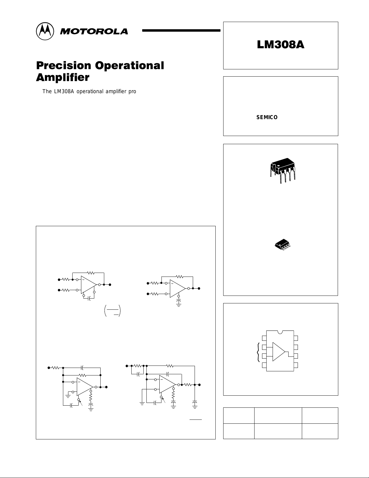
Frequency Compensation
Standard Compensation
Input
Input
R1
R3
Compen A
Inverting
Noninverting
+
R2
C
f
Cf
Compen B
≥
30
1 +
Output
1
R2
R1
Modified Compensation
Inverting
Noninverting
R1
Input
R3
Input
+
100 pF
R2
Output
Compen B
SUPER GAIN
OPERATIONAL AMPLIFIER
SEMICONDUCTOR
TECHNICAL DATA
8
1
N SUFFIX
PLASTIC PACKAGE
CASE 626
8
1
D SUFFIX
PLASTIC PACKAGE
CASE 751
(SO–8)
PIN CONNECTIONS
Standard Feedforward
Compensation
10 k
Input
500 pF
Compen A
5.0 pF
10
k
+
Compen B
3.0 k
10 pF
Output
Feedforward Compensations for
Decoupling Load Capacitance
RS > 10 k
Input
0.01
MOTOROLA ANALOG IC DEVICE DATA
Compen A Compen B
Inputs
100 k
10 pFC2*
µ
F
+
3.0 k
500 pF
Compen A
500
Compen B
10 pF
*C2 >
5 x 10
R2
Output
C
L
75 pF to
0.01
µ
F
5
pF
Device
LM308AN
LM308AD
Motorola, Inc. 1996 Rev 0
1
–
2
+
3
4
V
EE
(Top View)
ORDERING INFORMATION
Operating
Temperature Range
TA = 0° to +70°C
8
7
6
5
V
Output
NC
CC
Package
Plastic DIP
SO–8
1

LM308A
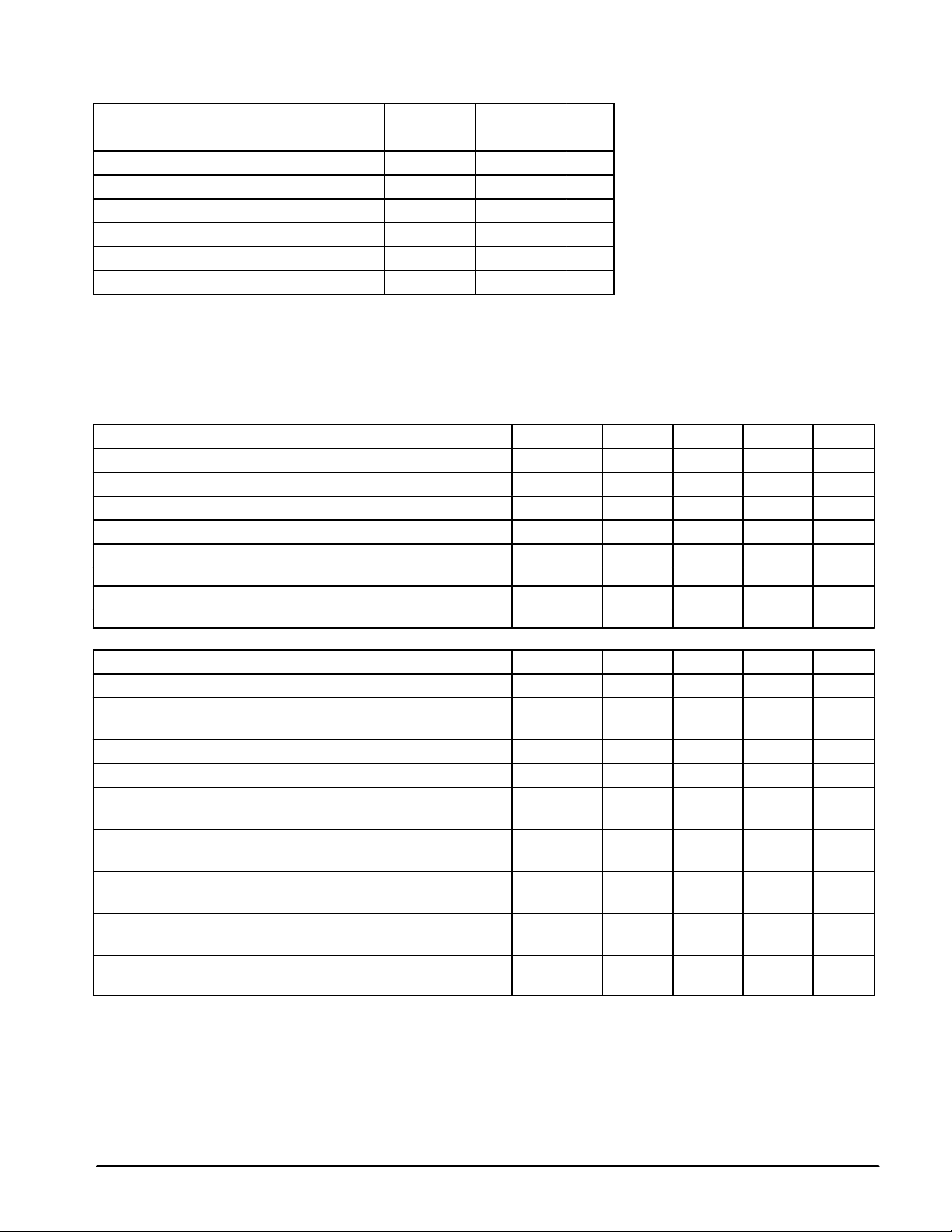
MAXIMUM RATINGS (T
Power Supply Voltage V
Input Voltage (See Note 1) V
Input Differential Current ( See Note 2) I
Output Short Circuit Duration t
Operating Ambient Temperature Range T
Storage Temperature Range T
Junction Temperature T
NOTES: 1. For supply voltages less than ±15 V , the maximum input voltage is equal to the supply
voltage.
2.The inputs are shunted with back–to–back diodes for overvoltage protection. Therefore,
excessive current will flow if a differential input voltage in excess of 1.0 V is applied
between the inputs, unless some limiting resistance is used.
ELECTRICAL CHARACTERISTICS (Unless otherwise noted these specifications apply for supply voltages of +5.0 V ≤ V
and –5.0 V ≥ VEE ≥ –15 V, TA = +25°C.)
Input Offset Voltage V
Input Offset Current I
Input Bias Current I
Input Resistance r
Power Supply Currents ICC, I
(VCC = +15 V, VEE = –15 V)
Large Signal Voltage Gain A
(VCC = +15 V, VEE = –15 V, VO = ±10 V, RL ≥ 10 kΩ)
The following specifications apply over the operating temperature range.
Input Offset Voltage V
Input Offset Current I
Average Temperature Coefficient of Input Offset Voltage ∆VIO/∆T – 1.0 5.0 µV/°C
TA (min) ≤ TA ≤ TA (max)
Average Temperature Coefficient of Input Offset Current ∆IIO/∆T – 2.0 10 pA/°C
Input Bias Current I
Large Signal Voltage Gain A
(VCC +15 V, VEE= –15 V, VO = ±10 V, RL ≥ 10 kΩ)
Input Voltage Range V
(VCC = +15 V, VEE= –15 V)
Common Mode Rejection CMR 96 110 – dB
(RS ≤ 50 kΩ)
Supply Voltage Rejection PSR 96 110 – dB
(RS ≤ 50 kΩ)
Output Voltage Range
(VCC = +15 V, VEE= –15 V, RL = 10 kΩ)
= +25°C, unless otherwise noted.)
A
Rating Symbol Value Unit
CC, VEE
I
ID
SC
A
stg
J
Characteristic
±18 Vdc
±15 V
±10 mA
Indefinite
0 to +70 °C
–65 to +150
+150 °C
Symbol Min Typ Max Unit
IO
IO
IB
i
VOL
IO
IO
IB
VOL
ICR
V
OR
°C
EE
≤ +15 V
CC
– 0.3 0.5 mV
– 0.2 1.0 nA
– 1.5 7.0 nA
10 40 – MΩ
– ±0.3 ±0.8 mA
80 300 – V/mV
– – 0.73 mV
– – 1.5 nA
– – 10 nA
60 – – V/mV
±14 – – V
±13 ±14 – V
2
MOTOROLA ANALOG IC DEVICE DATA

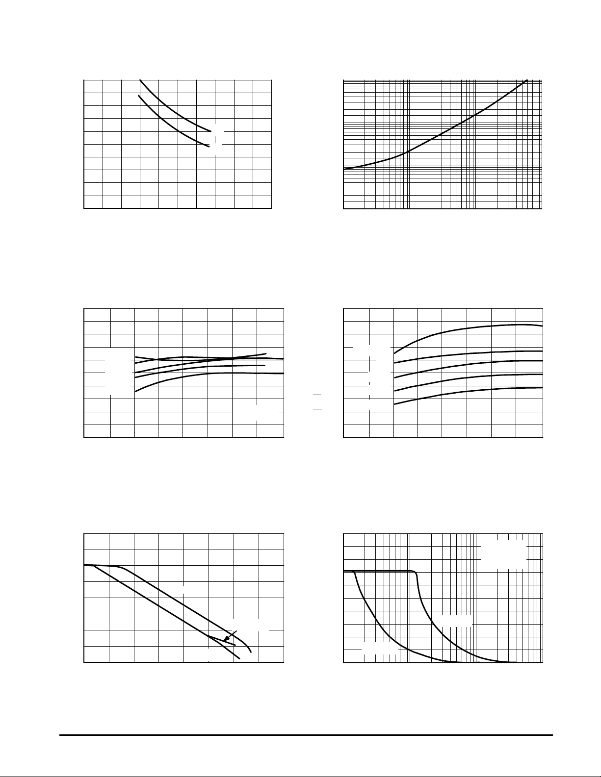
Figure 1. Input Bias and Input Offset Currents
2.0
1.8
1.6
1.4
1.2
1.0
0.8
, INPUT BIAS CURRENT (nA)
0.6
IB
I
0.4
0.2
0
–60 –40 –20 0 20 40 60 80 100 120 140
T, TEMPERATURE (°C) ri, INPUT RESISTANCE (Ω)
I
IO
I
IB
Figure 3. V oltage Gain versus Supply Voltages
130
120
TA = 0°C
110
100
, VOLTAGE GAIN (dB)
VOL
A
90
80
+25°C
–55°C
+70°C
+125°C
CF = 0
f = 100 Hz
0 5.0 10 15 20
VCC = VEE
, SUPPLY VOLTAGES (V)
LM308A
0.25
0.20
0.15
0.10
, INPUT OFFSET CURRENT (nA)
0.05
IO
I
0
Figure 2. Maximum Equivalent Input Offset
V oltage Error versus Input Resistance
100
10
1.0
0.1
EQUIVALENT INPUT OFFSET VOLTAGE (mV)
100 k 1.0 M 10 M 100 M
Figure 4. Power Supply Currents versus
Power Supply Voltages
500
µ
400
TA = –55°C
300
200
, SUPPLY CURRENTS ( A)
EE
I
100
=
CC
I
0
0 5.0 10
0°C
+25°C
+70°C
+125°C
VCC =
VEE
, SUPPLY VOLTAGES (V)
15 20
Figure 5. Open Loop Frequency Response Figure 6. Large Signal Frequency Response
140
120
100
80
60
40
, VOLTAGE GAIN (dB)
20
VOL
A
0
–20
1.0 10 100 1.0 k 10 k 100 k 1.0 M 10 M 100 M
CF = 3.0 pF
CF = 30 pF
CF = 100 pF
f, FREQUENCY (Hz) f, FREQUENCY (Hz)
MOTOROLA ANALOG IC DEVICE DATA
20
)
p–p
16
±
12
8.0
4.0
, OUTPUT VOL TAGE RANGE ( V
OR
V
CF = 30 pF
0
1.0 k 10 k 100 k 1.0 M
CF = 3.0 pF
VCC = +15 V
VEE = –15 V
°
C
TA = +25
3
 Loading...