Motorola CA2818C Datasheet

1
CA2818CMOTOROLA RF DEVICE DATA
The RF Line
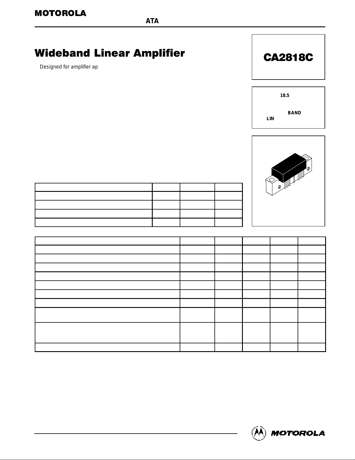
Designed for amplifier applications in 50 to 100 ohm systems requiring wide
bandwidth, low noise and low distortion. This hybrid provides excellent gain
stability with temperature and linear amplification as a result of the push–pull
circuit design.
• Specified Characteristics at VCC = 24 V, TC = 25°C:
Frequency Range — 0.35 to 400 MHz
Output Power — 1000 mW Typ @ 1 dB Compression, f = 200 MHz
Power Gain — 18.5 dB Typ @ f = 50 MHz
PEP — 1000 mW Typ @ –32 dB IMD, f = 200 MHz
Noise Figure — 5 dB Typ @ f = 200 MHz
ITO — 47 dBm Typ @ f = 150 MHz
• All Gold Metallization for Improved Reliability
• Unconditional Stability Under All Load Conditions
MAXIMUM RATINGS
Rating Symbol Value Unit
Supply Voltage V
CC
28 Vdc
RF Power Input P
in
+14 dBm
Operating Case Temperature Range T
C
–20 to +100 °C
Storage Temperature Range T
stg
–40 to +100 °C
ELECTRICAL CHARACTERISTICS (T
C
= 25°C, VCC = 24 V, 50 Ω system unless otherwise noted)
Characteristic
Symbol Min Typ Max Unit
Frequency Range BW 0.35 — 400 MHz
Gain Flatness (f = 0.35–400 MHz) F
L
— ±0.5 ±1 dB
Power Gain (f = 50 MHz) P
G
17.75 18.5 19.25 dB
Noise Figure, Broadband (f = 200 MHz) NF — 5 6 dB
Power Output — 1 dB Compression (f = 200 MHz) Po
1dB
800 1000 — mW
Third Order Intercept (See Figure 10, f1 = 200 MHz) ITO 43 45 — dBm
Input/Output VSWR (f = 0.35–400 MHz) VSWR — 1.7:1 2:1 —
Second Harmonic Distortion (Po = 100 mW) f2H = 0.35–200 MHz
f2H = 200–400 MHz
d
so
—
—
–65
—
–60
–50
dB
Peak Envelope Power (Two Tone Distortion Test — See Figure 10)
f = 0.35–200 MHz @ –32 dB IMD
f = 200–400 MHz @ –32 dB IMD
PEP 600 800 — mW
Supply Current I
CC
190 205 220 mA
Order this document
by CA2818C/D
SEMICONDUCTOR TECHNICAL DATA
18.5 dB
0.35–400 MHz
1000 mWATT
WIDEBAND
LINEAR AMPLIFIER
CASE 714F–03, STYLE 1
[CA (POS. SUPPLY)]
Motorola, Inc. 1995
REV 1

CA2818C
2
MOTOROLA RF DEVICE DATA
TYPICAL CHARACTERISTICS
f, FREQUENCY (MHz)
100 7006005004003002000
20
19
18
17
16
15
14
13
PG, POWER GAIN (dB)
TC = 25°C
15 V
24 V
28 V
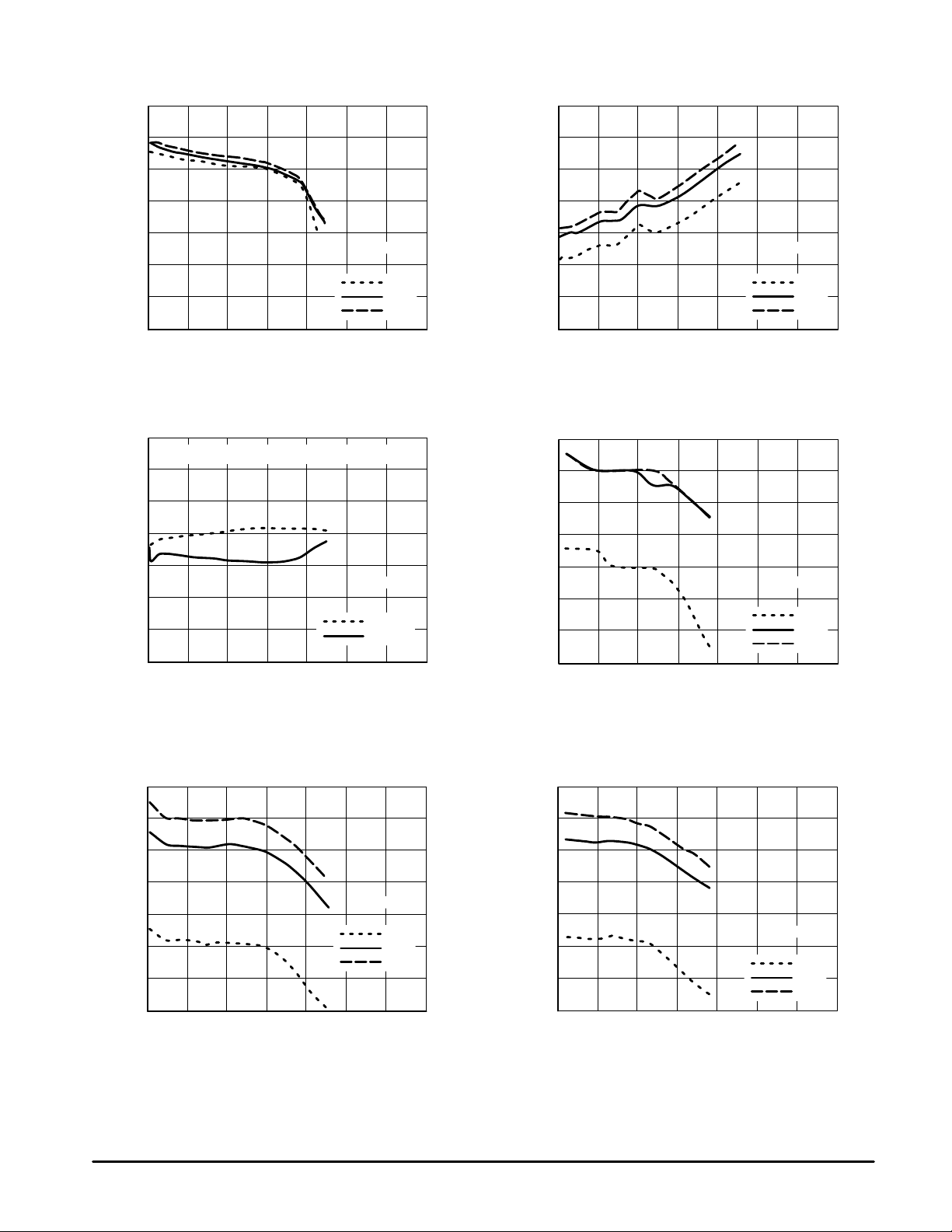
Figure 1. Power Gain versus Voltage
VCC = 24 V
f, FREQUENCY (MHz)
100 7006005004003002000
1.5
GAIN (dB)
∆
1.0
0.5
0.0
– 0.5
– 1.0
– 1.5
– 2.0
– 40°C
+ 100
°
C
(RELATIVE TO FREQUENCY RESPONSE AT 25°C)
Figure 2. Relative Power Gain
versus Temperature
f, FREQUENCY (MHz)
100 7006005004003002000
TC = 25°C
34
32
30
28
26
24
22
20
Po1dB, POWER OUTPUT (dBm)
15 V
24 V
28 V
Figure 3. 1 dB Compression versus Voltage
TC = 25°C
f, FREQUENCY (MHz)
100 7006005004003002000
8
7
6
5
4
3
2
1
NF, NOISE FIGURE (dB)
15 V
24 V
28 V
Figure 4. Noise Figure versus Voltage
TC = 25°C
f, FREQUENCY (MHz)
100 7006005004003002000
47
45
43
41
39
37
35
33
ITO, 3RD ORDER INTERCEPT POINT (dBm)
15 V
24 V
28 V
Figure 5. Third Order Intercept
versus Voltage
f, FREQUENCY (MHz)
100 7006005004003002000
TC = 25°C
34
32
30
28
26
24
22
20
PEP, POWER (dBm)
15 V
24 V
28 V
Figure 6. Peak Envelope Power
versus Voltage
 Loading...