

Page 1
V1.0
C168
Level 3
Debug Guide
10/31/05
Page 2

INDEX
1. Debug guide.............................................................................................................................3
1.1 Baseband circuit Debug guide...................................................................................... 3
1.1.1 Phone is Dead ....................................................................................................... 3
1.1.2 SIM Card Detection Error .................................................................................... 4
1.1.3 Audio Fail............................................................................................................. 5
1.1.3.1 Headset Fail..................................................................................................... 5
1.1.3.2 Speaker Fail..................................................................................................... 6
1.1.3.3 Handset Microphone Fail............................................................................... 7
1.1.3.4 Earphone Speaker Fail...................................................................................8
1.1.4 LCM Fail .............................................................................................................. 8
1.1.5 Charger Fail .......................................................................................................... 9
1.1.6 Vibrator Fail........................................................................................................ 10
1.1.7 FM function Fail................................................................................................. 10
1.2 Radio Frequency circuit troubleshooting................................................................... 11
1.2.1 26MHz System clock fail ................................................................................... 11
1.2.2 RF signal diagram in GSM900 Tx mode............................................................ 12
1.2.3 RF signal diagram in DCS1800 TX mode.......................................................... 13
1.2.4 RF signal diagram in GSM900 Rx mode ........................................................... 14
1.2.5 RF signal diagram in DCS1800 RX mode..........................................................15
2
Page 3
1. Debug guide
1.1 Baseband circuit Debug guide
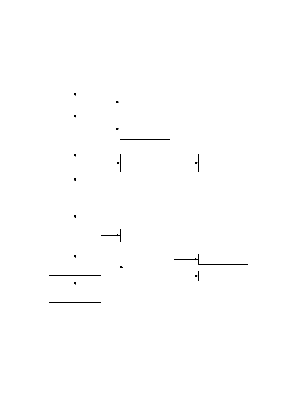
1.1.1 Phone is Dead
The phone is dead
Voltage at C620 =3.6V
Yes
Voltage at
C210=3.6V
C215=1.5V(VRRTC)
TP211=1.5V(RESPWON)
Yes
Clock at TP210
=~ 32.768KHz
Yes
Press PWON and then we
can detect falling edge at
TP207
Voltage at
C213=1.8V(VRRAM)
C212=1.8V(VRMEM)
C217=1.5V(VRDBB)
C211=2.8V(VRIO)
C216=2.8V(VRABB)
NO
NO
NO
NO
Contact problem
Defective IOTA (U202) or
PCB
Check R205 whether
32768Hz is available
Defective IOTA (U202 ) or PCB
Defective Calypso (U201),
X201 or PCB
Yes
Clock at C201
= 26M Hz
Yes
See section
"Download Failed"
NO
Check status of Pin3 of
U601 is high (TCXOEN).
NO
Yes
Defective CALYPSO
(U201) or PCB
Please refer to RF part
Faulting Finding Chart of “Phone is Dead”
3
Page 4
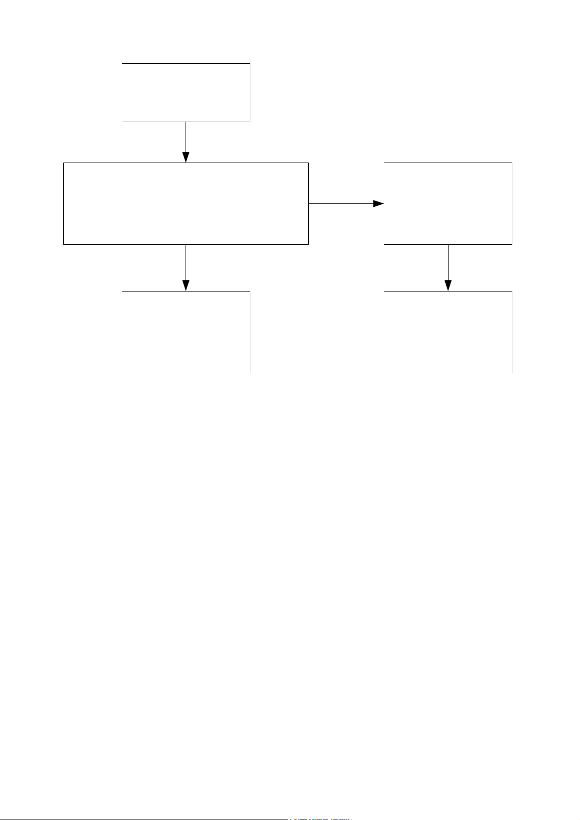
1.1.2 SIM Card Detection Error
SIM Card
Detection Error
Check if signal level at
VRSIM=1.8 / 3.0V , SIMRST,
SIMCLK(=3.25MHz), SIMIO
Are correct
YES
Check SIM Card
Type or SIM Card
if well inserted
Fault Finding Chart of “SIM Card Error”
NO
Check SIM socket
Soldering well
YES
Defective IOTA
U202
4
Page 5

1.1.3 Audio Fail
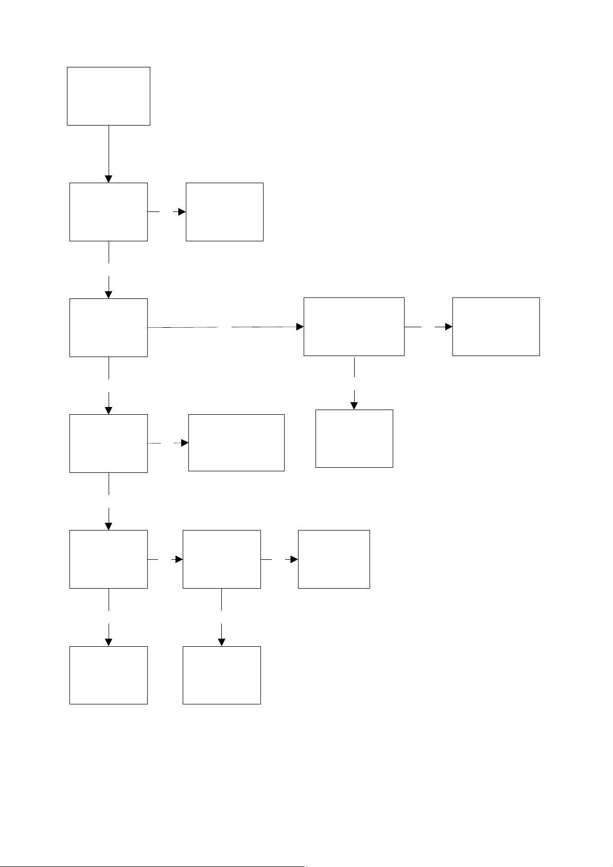
1.1.3.1 Headset Fail
Earphone doesn't work
Defective J102
YES
Insert Earphone and
check if handset mode
is detected
YES
Measure AC Signal of
L101 ( R ) & L106 ( L )
YES
NO
NO
Check R112 if any level
change
Check U102_PIN6 if
any level change
Check AC signal at
U102 Pin 4?
Check AC signal at
U105 Pin10, 11 (input)
& Pin 14, 15 (output)
Check U104 Pin 4 & 8
if any level change
Check AC signal at U104
Pin3(COM1), 2(NO), 5(NC)
Pin9(COM2), 10(NO), 7(NC)
YES
U105 is OK
YES
Defective J102 or , R112
NO
NO
NO
NO
and R117,R118 are not
well mounted
Defective CALYPSO
NO
NO
U201
Defective U102
Defective U105
Defective U201
Defective U104
Measure Signal
(Microphone) of L102
YES
Measure Signal
(EP_status) of R112
YES
Defective U201
If Pin 5 is abnormal, then Defective U202
If Pin 2 is abnormal, then Defective U702
NO
NO
Check J102 are well
mounted
YES
Check if Earpiece is
plugged in well
Check J102_PIN4 if any
level change
Yes
Defective U201,U202
NO
Defective J102 and L104
Fault Finding Chart of “Headset fail”
Defective J102
are not well mounted
5
Page 6

1.1.3.2 Speaker Fail
Speaker doesn't work
Check if speaker is
well contacted
YES
Check CN401 Pin12,
14, 16 and 18
YES
Measure speaker
signal on L31, C308,
C309
YES
NO
NO
NO
Defective Speaker
Defective CN401 B2B
connector
Defective U101, U201,
L31
Check mechanical
fabrication
Faulting Finding Chart of “Speaker fail”
6
Page 7

1.1.3.3 Handset Microphone Fail
Microphone doesn't work
Measure L105, C111 and
C112 any AC signal
Yes
Check if CN401 contact well
Yes
Check if MIC FPC pad TP1,
TP2 solder well
Yes
No
No
No
Defective U202
Defective CN401
Check MIC FPC
Solder process
Defective MIC
Faulting Finding Chart of “Microphone fail”
7
Page 8

1.1.3.4 Earphone Speaker Fail
Earphone doesn't
work
any AC signal change
Check L32 If any AC signal
1.1.4 LCM Fail
Check R315, R316 If
YES
change
YES
Check Earphone
Impendence is
32 Ohm
Faulting Finding Chart of “Receiver fail”
NO
NO
Check R315, R316
solderring
Defective L32
Defective Earphone
YES
LCD does not work
Check if CN301 is well
mounted
YES
Measure Signal of
CON301 Pin 4, 14 is 1.8V ?
NO
NO
Defective connector
CON301
Defective U202
YES
Measure Signal of
CON301 Pin5 ~ Pin12 any
Defective U201
signal wave ?
Faulting Finding Chart of “LCD fail”
8
Page 9

1.1.5 Charger Fail
Charger does not work
Measure CON303
Pin 3 have voltage
> 4.0V ?
YES
Measure U304 Pin 1 & 3
is 0V ?
YES
Measure U308 Pin 7, 8 have
voltage > 4.0V ?
YES
Measure
U310 Pin 2 and Pin 3 > 4.0V
& U306 Pin 3, Pin 4, Pin 5 > 4.0V
& U302 in/out put > 4.0V
NO
NO
NO
NO
Defective CON303
Defective U304
Defective U308
Defective U310
or U306 or U302
YES
Measure U308 Pin 5, 6 have
voltage > 4.0V ?
YES
YES
Faulting Finding Chart of “Charger fail”
NO
Defective U308
NO
Maybe R303 bad solderMeasure R303 voltage > 4.0 V
NO
Defective U301Measure U301 Pin 2 = 0V
9
Page 10

1.1.6 Vibrator Fail
Vibrator does not work
Measure the signal
of Vibrator_on at R406
Defective U41
1.1.7 FM function Fail
FM function Failed
Check C703, C707, R708
is well mounted
NO
> 2.8V
YES
Defective U202
Faulting Finding Chart of “Vibrator failed”
NO
Defective solder
C706, C707, R703
YES
Check I2C Signal at
R705, R706
NO
Defective U201
YES
Check U702 Pin 15 AFR
& Pin 16 AFL
NO
Defective U702
Is AC Signal
YES
Check Audio path
Faulting Finding Chart of “FM function faults”
10
Page 11

1.2 Radio Frequency circuit troubleshooting
1.2.1 26MHz System clock fail
No 26MHz clock
Check if U601 Pin 5 is
2.8V
Yes
Check U606 Pin 1
or U606 Pin 3 If
26MHz Sine wave
exists
Yes
Check U604 Pin 8 If
26MHz Sine wave
exists
No
Defective U606No
No Replace U604
Check if U601 Pin 1
> 3.2V
Yes
Check if U601 Pin 3
> 2.8V
Yes
Defective U602
(voltage regulator)
Fault Finding chart of 26MHz clock part
No
No
Check Battery Cell is
empty ?
Defective U201 or
U202
11
Page 12

1.2.2 RF signal diagram in GSM900 Tx mode
GSM900 Tx fail
(BB lives)
Check if R603, C611
has modulaed RF signal
Yes
Check if C613 has
amplified RF signal
Yes
Check if C617 has
amplified RF signal
Yes
Defective CON601
Check if U607 Pin
NO
10 > 2.8V & U607
Defective U607
No
Check if
TP614 has
ramp signal
Yes
Defective
U605 (PA)
No
Defective
U202 or
Pin 2 = 0V
Yes
(T/R switch)
No
Defective U608
No
or U201
Fault Finding chart of GSM900 Tx part
U201
Check if
TP605~608
have Sine wave
Yes
Defective U604
No
Defective U201
or U202
12
Page 13

1.2.3 RF signal diagram in DCS1800 TX mode
DCS1800 Tx fail
(BB lives)
Check if R602, C6 12
has modulated RF
signal
Yes
Check if C623 has
amplified RF signal
Yes
Check if C617 has
amplified RF signal
Yes
Defective CON601
Check if U607 Pin
NO
10 = 0V & U607 Pin
2 > 2.8V
Defective U607
No
Yes
No
TP614 has
ramp signal
U605 (PA)
No
Defective U608
or U201
Check if
Yes
Defective
No
Defective
U202
Check if
TP605~608
have TxIQ sin
wave
Yes
Defective U604
No
Defective U201
or U202
Fault Finding chart of DCS1800 Tx part
13
Page 14

1.2.4 RF signal diagram in GSM900 Rx mode
GSM900 Rx fail
(BB Lives)
Check if C617
has input RF
signal
Yes
Check if L606
has input RF
signal
Yes
Check if C609,
C610 has input
RF signal
No
No
Defective
CON601
No
Defective
U602 or L606
Check if
U607 Pin 10 = 0V
& U607 Pin 2 = 0V
Yes
Defective U607
No
Defective U608
or U201
Yes
Check
TP605~608 if
RxIQ waveform
is correct
Yes
Defective U202
Check if U604
Pin 1, Pin2 and
No
Pin3 has correct
Defective U604
No
waveform
Yes
Defective
U201
Fault Finding chart of GSM900 Rx part
14
Page 15
1.2.5 RF signal diagram in DCS1800 RX mode
DCS1800 Rx fail
(BB Lives)
Check if C617
has input RF
signal
Yes
Check if L607
has input RF
signal
Yes
Check if C607,
C608 has input
RF signal
No
No
Defective
CON601
No
Defective U603 or
L607
Check if U607 Pin
10 = 0V& U607 Pin
2 = 0V
Yes
Defective U607
No
Defective U608 or
U201
Yes
Check
TP605~608 if
RxIQ waveform
is correct
Yes
Defective U202
Check if U604
No
Pin 1, Pin2 and
Pin3 has correct
Defective U604
No
waveform
Yes
Defective
U201
Fault Finding chart of DCS1800 Rx part
15
 Loading...