

Mitsubishi M5M4V4S40CTP-15, M5M4V4S40CTP-12 Datasheet

SDRAM (Rev. 0.3)
MITSUBISHI LSIs
Feb ‘97 Preliminary
M5M4V4S40CTP-12, -15
4M (2-BANK x 131072-WORD x 16-BIT) Synchronous DRAM
PRELIMINARY
Some of contents are described for general products
and are subject to change without notice.
DESCRIPTION
The M5M4V4S40CTP is a 2-bank x 131,072-word x 16-bit
Synchronous DRAM, with LVTTL interface. All inputs and
outputs are referenced to the rising edge of CLK. The
M5M4V4S40CTP achieves very high speed data rates up to
83MHz, and is suitable for main memory or graphic memory
in comp uter systems.
FEATURES
- Single 3.3v±0.3v power supply
- Clock frequency 83MHz / 67MHz
- Fully synchronous operation referenced to clock rising edge
- Dual bank operation controlled by BA(Bank Address)
- /CAS latency- 1/2/3 (programmable)
- Burst length- 1/2/4/8/FP (programmable)
- Sequential and interleave burst (programmable)
- Byte control by DQMU and DQML
- Random column access
- Auto precharge / All bank precharge controlled by A8
- Auto and self refresh
- 1024 refresh cycles /16.4ms
- LVTTL Inter fac e
- 400-mil, 50-pin Thin Small Outline Package
(TSOP II) with 0.8mm lead pitch
Max.
Frequency
M5M4V4S40CTP-12 83MHz 8ns
CLK Access
Time
Vdd
DQ0
DQ1 DQ14
VssQ
DQ2
DQ3
VddQ
DQ4
DQ5 DQ10
VssQ VssQ
DQ6 DQ9
DQ7 DQ8
VddQ VddQ
DQML
/WE
/CAS
/RAS
/CS
BA
A8
A0
A1
A2
A3
Vdd
CLK : Master Clock
CKE : Clock Enable
/CS : Chip Select
/RAS : Row Address Strobe
/CAS : Column Address Strobe
/WE : Write Enable
DQ0-15 : Data I/O
DQMU : Upper Output Disable/ Write Mask
DQML : Lower Output Disable/ Write Mask
A0-8 : Address Input
BA : Bank Address
Vdd : Power Supply
VddQ : Power Supply for Output
Vss : Ground
VssQ : Ground for Output
PIN CONFIGURATION
(TOP VIEW)
1
2
3
4
5
6
7
8
9
10
11
12
13
14
15
16
17
18
19
20
21
22
23
24
25
400mil 50pin TSOP(II)
50
49
48
47
46
45
44
43
42
41
40
39
38
37
36
35
34
33
32
31
30
29
28
27
26
Vss
DQ15
VssQ
DQ13
DQ12
VddQ
DQ11
NC
DQMU
CLK
CKE
NC
NC
NC
A7
A6
A5
A4
Vss
M5M4V4S40CTP-15 67MHz 9ns
MITSUBISHI ELECTRIC
1

SDRAM (Rev. 0.3)
MITSUBISHI LSIs
Feb ‘97 Preliminary
4M (2-BANK x 131072-WORD x 16-BIT) Synchronous DRAM
BLOCK DIAGRAM
Mode
Register
Memory Array
Bank #0
M5M4V4S40CTP-12, -15
DQ0-15
I/O Buffer
Memory Array
Bank #1
Address Buffer
A0-8 BA
Clock Buffer
CLK CKE
Type Designation Code
M 5M 4 V 4 S 4 0 C TP - 12
Control Circuitry
Control Signal Buffer
/CS /RAS /CAS /WE DQML
These rules are only applied to the Synchronous DRAM family.
Cycle Time (min.) 12: 12ns, 15: 15ns
Package Type TP: TSOP(II)
Process Generation
Function 0: Random Column, 1: 2N-rule
Organization 2n 4: x16
Synchronous DRAM
Density 4:4M bits
Interface V:LVTTL
Memory Style (DRAM)
Use, Recommended Operati ng Conditions, etc
Mitsubishi Mai n Designation
DQMU
MITSUBISHI ELECTRIC
2

SDRAM (Rev. 0.3)
MITSUBISHI LSIs
Feb ‘97 Preliminary
M5M4V4S40CTP-12, -15
4M (2-BANK x 131072-WORD x 16-BIT) Synchronous DRAM
PIN FUNCTION
CLK Input Master Clock: All other input s ar e refer enc ed to the rising edge of CLK.
Clock Enable: CKE controls the int er nal clock. When CKE is low, the
CKE Input
/CS Input Chip Select: When /CS is high, all commands are inhibited.
/RAS, /CAS, /WE In put /RAS, /CAS , and /WE are used to def ine bas ic co mmands.
A0-8 Input
internal clock for the following cycle is disabled. CKE is also used to select
auto and self refresh. After self- r efresh mode is started, CKE acts as an
asynchronous input to maintain and exit the mode.
A0-8 specify the Row and Column addresses within the selected bank.
The Row Address is set by A0-8 and the Column Address is s et by A0-7.
A8 is also used to indicate the precharge option. When A8 is high during
read or write command, an auto prechar ge is per form ed. When A8 is
high during a precharge command, both banks are precharged.
Bank Address: BA is not simply A9. BA specifies the bank to which a
BA Input
DQ0-15 Input / Output Data In and data out are referenced to t he r is ing edge of CLK.
DQML Input
DQMU Input
Vdd, Vss Power Supply Power Supply for the memory array and per ipheral circuitr y.
VddQ, VssQ Power Supply Power Supply for the outp ut buf fers only .
command is applied. BA must be set during the ACT, PRE, READ,
and WRITE commands.
Lower Din(0-7) Mask; Lower Dout(0-7) Disable; When DQML is high
during burst write Din( 0- 7) for the cur r ent cycle is masked. When DQML
is high during burst read Dout(0-7) is disabled two cycles later.
Upper Din(8-15) Mask; Uppe r Dout( 8- 15) Dis able; When DQMU is high
during burst write Din( 8- 15) for the cur r ent cy c le is masked. When DQMU
is high during burst read Dout(8-15) is disabled two cycles later.
MITSUBISHI ELECTRIC
3
SDRAM (Rev. 0.3)
MITSUBISHI LSIs
Feb ‘97 Preliminary
M5M4V4S40CTP-12, -15
4M (2-BANK x 131072-WORD x 16-BIT) Synchronous DRAM
BASIC FUNCTIONS
The M5M4V4S40CTP has the following basic functions, bank (row) activate, burst read/write, bank
(row) precharge, and auto/self refresh. Each command is defined by the control signals (/RAS, /CAS and
/WE) at the rising edge of CLK. The inputs /CS ,CKE and A8 are used for chip select, refresh options, and
precharge options, respectively.
Please see the command truth table for detailed definitions.
CLK
/CS
/RAS
/CAS
/WE
CKE
A8
Chip Select : L=select, H=deselect
Command
Command
Command
Refresh Option @refresh command
Precharge Option @precharge or read/write command
define basic commands
Activate (ACT) [/RAS =L, /CAS =/WE =H]
The ACT command activates a row in an idle bank. The bank address, BA, is used to select which of
the two banks wi ll be ac tiva ted.
Read (READ) [/RAS =H, /CAS =L, /WE =H]
The READ command starts burst read from the active bank indicated by BA. The first output data
appears afte r /CA S latency. If A8 =H whe n R EA D is i ssu ed the bank is au tom a tic ally prech a rge d af te r
the last burst read (READA). Note: READA is no t valid for FP b urs t operat io ns.
Write (WRITE) [/RAS =H, /CAS =/WE =L]
The WRITE command starts burst write to the active bank indicat ed by BA. Total data length t o be
written is set by burst length. If A8 =H when WRITE is issued the bank is automatically precharged
after the last burst write (WRITEA). No te : WRI TEA is not valid fo r FP bur st op eratio ns .
Precharge (PRE) [/RAS =L, /CAS =H, /WE =L]
The PRE command deactivates the active bank indicated by BA. This command also terminates burst
read and write operations. If A8 =H when PRE is issued both banks are automatically precharged (PREA).
Auto-Refresh (REFA) [/RAS =/CAS =L, /WE =CKE =H]
The REFA command starts an auto-refresh cycle. The refresh address, including the bank address, is
generated internally. After this command, the banks are precharged automatically.
MITSUBISHI ELECTRIC
4

SDRAM (Rev. 0.3)
MITSUBISHI LSIs
Feb ‘97 Preliminary
M5M4V4S40CTP-12, -15
4M (2-BANK x 131072-WORD x 16-BIT) Synchronous DRAM
COMMAND TRUTH TABLE
COMMAND MNEMONIC
Deselect DESEL H X H X X X X X X
No Operation NOP H X L H H H X X X
Row Address Entry &
Bank Activate
Single Bank Precharge PRE H X L L H L V L X
Precharge All Banks PREA H X L L H L X H X
Column Address Entry
& Write
Column Address Entry
& Write with Auto Precharge
ACT H X L L H H V V V
WRITE H X L H L L V L V
WRITEA H X L H L L V H V
CKE
n-1
CKE
n
/CS /RAS /CAS /WE BA A8 A0-7
Column Address Entry
& Read
Column Address Entry
& Read with Auto Precharge
Auto-Refresh REFA H H L L L H X X X
Self-Refresh Entry REFS H L L L L H X X X
Self-Refresh Exit REFSX
Burst Terminate TBST H X L H H L X X X
Mode Register Set MRS H X L L L L V L V*1
H=High Level, L=Low Level, V=Valid, X=Don’t Care, n=CLK cycle number
NOTE:
1. A7 =0, A0-A6 =Mode Address
READ HXLHLHVLV
READA H X L H L H V H V
LHHXXXXXX
LHLHHHXXX
MITSUBISHI ELECTRIC
5

SDRAM (Rev. 0.3)
MITSUBISHI LSIs
Feb ‘97 Preliminary
M5M4V4S40CTP-12, -15
4M (2-BANK x 131072-WORD x 16-BIT) Synchronous DRAM
FUNCTION TRUTH TABLE
Current State /CS /RAS /CAS /WE Address Command Action
IDLE H X X X X DESEL NOP
LHHHX NOP NOP
L H H L X TBST ILLEGAL*2
L H L X BA, CA, A8 READ / WRITE ILLEGAL*2
L L H H B A , RA ACT Bank Active, Latch RA
L L H L BA, A8 PRE / PREA NOP*4
L L L H X REFA Auto-Refresh*5
LLLL
ROW ACTIVE H X X X X DESEL NOP
LHHHX NOP NOP
LHHLX TBST NOP
Op-Code,
Mode-Add
MRS Mode Register Set*5
L H L H BA , CA, A8 READ / READA
L H L L BA, CA, A8
L L H H BA, RA ACT Bank Active / ILLEGAL*2
L L H L BA, A8 PRE / PREA Precharge / Precharge All
L L L H X REFA ILLEGAL
LLLL
READ H X X X X DESEL NOP (Continue Burst to END)
L H H H X NOP NOP (Continue Burst to END)
L H H L X TBST Terminate Burst
L H L H BA , CA, A8 READ / READA
L H L L BA, CA, A8
Op-Code,
Mode-Add
WRITE /
WRITEA
MRS ILLEGAL
WRITE /
WRITEA
Begin Read, Latch CA,
Determine Auto-Prechar ge
Begin Write, Latch CA,
Determine Auto-Prechar ge
Terminate Burst, Latch CA,
Begin New Read, Determine
Auto-Precharge*3
Terminate Burst, Latch CA,
Begin Write, Determine AutoPrecharge*3
L L H H BA, RA ACT Bank Active / ILLEGAL*2
L L H L BA, A8 PRE / PREA Terminate Burst, Precharge
L L L H X REFA ILLEGAL
LLLL
Op-Code,
Mode-Add
MRS ILLEGAL
MITSUBISHI ELECTRIC
6

SDRAM (Rev. 0.3)
MITSUBISHI LSIs
Feb ‘97 Preliminary
M5M4V4S40CTP-12, -15
4M (2-BANK x 131072-WORD x 16-BIT) Synchronous DRAM
FUNCTION TRUTH TABLE (continued)
Current State /CS /RAS /CAS /WE Address Command Action
WRITE H X X X X DESEL NOP (Continue Burst to END)
L H H H X NOP NOP (Continue Burst to END)
L H H L X TBST Terminate Burst
Terminate Burst, Latch CA,
L H L H BA , CA, A8 READ / READA
L H L L BA, CA, A8
L L H H BA, RA ACT Bank Active / ILLEGAL*2
L L H L BA, A8 PRE / PREA Terminate Burst, Precharge
L L L H X REFA ILLEGAL
LLLL
Op-Code,
Mode-Add
WRITE /
WRITEA
MRS ILLEGAL
Begin Read, Determine AutoPrecharge*3
Terminate Burst, Latch CA,
Begin Write, Determine AutoPrecharge*3
READ with
AUTO
PRECHARGE
WRITE with
AUTO
PRECHARGE
H X X X X DE SEL NOP (Continue Burst to END)
L H H H X NOP NOP (Continue Burst to END)
L H H L X TBST ILLEGAL
L H L H BA, CA, A8 READ / READA ILLEGAL
L H L L BA, CA, A8
L L H H BA, RA ACT Bank Active / ILLEGAL*2
L L H L BA, A8 PRE / PREA ILLEGAL*2
L L L H X REFA ILLEGAL
LLLL
H X X X X DE SEL NOP (Continue Burst to END)
L H H H X NOP NOP (Continue Burst to END)
L H H L X TBST ILLEGAL
L H L H BA, CA, A8 READ / READA ILLEGAL
L H L L BA, CA, A8
Op-Code,
Mode-Add
WRITE /
WRITEA
MRS ILLEGAL
WRITE /
WRITEA
ILLEGAL
ILLEGAL
L L H H BA, RA ACT Bank Active / ILLEGAL*2
L L H L BA, A8 PRE / PREA ILLEGAL*2
L L L H X REFA ILLEGAL
LLLL
Op-Code,
Mode-Add
MRS ILLEGAL
MITSUBISHI ELECTRIC
7

SDRAM (Rev. 0.3)
MITSUBISHI LSIs
Feb ‘97 Preliminary
M5M4V4S40CTP-12, -15
4M (2-BANK x 131072-WORD x 16-BIT) Synchronous DRAM
FUNCTION TRUTH TABLE (continued)
Current State /CS /RAS /CAS /WE Address Command Action
PRE CHARGING
ROW
ACTIVATING
H X X X X DESEL NOP (Idle after tRP)
L H H H X NOP NOP (Idle after tRP)
L H H L X TBST ILLEGAL*2
L H L X BA, CA, A8 READ / WRITE ILLEGAL*2
L L H H BA, RA ACT ILLEGAL*2
L L H L BA, A8 P RE / PREA NOP*4 (Idle after tRP)
L L L H X REFA ILLEGAL
LLLL
H X X X X DESEL NOP (Row Active after tRC D)
L H H H X NOP NOP (Row Active after tRCD)
L H H L X TBST ILLEGAL*2
Op-Code,
Mode-Add
MRS ILLEGAL
WRITE RECOVERING
L H L X BA, CA, A8 READ / WRITE ILLEGAL*2
L L H H BA, RA ACT ILLEGAL*2
L L H L BA, A8 PRE / PREA ILLEGAL*2
L L L H X REFA ILLEGAL
LLLL
H X X X X DESEL NOP
LHHHX NOP NOP
L H H L X TBST ILLEGAL*2
L H L X BA, CA, A8 READ / WRITE ILLEGAL*2
L L H H BA, RA ACT ILLEGAL*2
L L H L BA, A8 PRE / PREA ILLEGAL*2
L L L H X REFA ILLEGAL
LLLL
Op-Code,
Mode-Add
Op-Code,
Mode-Add
MRS ILLEGAL
MRS ILLEGAL
MITSUBISHI ELECTRIC
8
SDRAM (Rev. 0.3)
MITSUBISHI LSIs
Feb ‘97 Preliminary
M5M4V4S40CTP-12, -15
4M (2-BANK x 131072-WORD x 16-BIT) Synchronous DRAM
FUNCTION TRUTH TABLE (continued)
Current State /CS /RAS /CAS /WE Address Command Action
REFRESHING
MODE
REGISTER
SETTING
H X X X X DESEL NOP (Idle after tRC)
L H H H X NOP NOP (Idle after tRC)
L H H L X TBST ILLEGAL
L H L X BA, CA, A8 READ / WRITE ILLEGAL
L L H H BA, RA ACT ILLEGAL
L L H L BA, A8 PRE / PREA ILLEGAL
L L L H X REFA ILLEGAL
LLLL
H X X X X DESEL NOP (Idle after tRSC)
L H H H X NOP NOP (Idle after tRSC)
L H H L X TBST ILLEGAL
Op-Code,
Mode-Add
MRS ILLEGAL
L H L X BA, CA, A8 READ / WRITE ILLEGAL
L L H H BA, RA ACT ILLEGAL
L L H L BA, A8 PRE / PREA ILLEGAL
L L L H X REFA ILLEGAL
LLLL
ABBREVIATIONS:
H=High Level, L=Low Level, X=Don’t Care
BA=Bank Address, RA=Row Address, CA=Column Address, NOP=No Operation
NOTES:
1. All entries assume that CKE was High during the preceding clock cycle and the current clock cycle.
2. ILLEGAL to bank in specified state; function may be legal in the bank indicated by BA, depending on the state of
that bank.
3. Must satisfy bus contention, bus turn around, write reco very r equir em ents.
4. NOP to bank precharging or in idle state. May precharge bank indicated by BA.
5. ILLEGAL if any bank is not idle.
ILLEGAL = Device operation and/or data-integrity are not guaranteed.
Op-Code,
Mode-Add
MRS ILLEGAL
MITSUBISHI ELECTRIC
9

SDRAM (Rev. 0.3)
MITSUBISHI LSIs
Feb ‘97 Preliminary
M5M4V4S40CTP-12, -15
4M (2-BANK x 131072-WORD x 16-BIT) Synchronous DRAM
FUNCTION TRUTH TABLE for CKE
Current State
SELFREFRESH*1
POWER
DOWN
ALL BANKS
IDLE*2
CKE
CKE
n-1
HXXXXXXINVALID
L H H X X X X Exit Self - Refresh (Idle after tRC)
L H L H H H X Exit Self - Refresh (Idle after tRC)
LHLHHLXILLEGAL
LHLHLXXILLEGAL
L H L L X X X ILLEGAL
L L X X X X X NOP (Maintain Self -Re fres h)
HXXXXXXINVALID
L H X X X X X Exit Power Down to Idle
L L X X X X X NOP (Maintain Self -Re fres h)
H H X X X X X Refer to Function Truth Table
H L L L L H X Enter Self-Refr es h
/CS /RAS /CAS /WE Add Action
n
H L H X X X X Enter Power Down
H L L H H H X Enter Power Down
H L L H H L X ILLEGAL
H L L H L X X ILLEGAL
H L L L X X X ILLEGAL
L X X X X X X Refer to Current State =Power Down
ANY STATE
other than
listed above
ABBREVIATIONS:
H=High Level, L=Low Level, X=Don’t Care
NOTES:
1. CKE Low to High transition wil l re-enable CLK and other inputs asynchron ous ly . A minimum setup time must be
satisfied before any command other than EXIT.
2. Power-Down and Self-Refresh can be entered only from the All Banks Idle State.
3. Must be legal command.
H H X X X X X Refer to Function Truth Table
H L X X X X X Begin CLK Suspend at Next Cycle*3
L H X X X X X Exit CLK Suspend at Next Cycle*3
L L X X X X X Maintain CLK Suspend
MITSUBISHI ELECTRIC
10

SDRAM (Rev. 0.3)
MITSUBISHI LSIs
Feb ‘97 Preliminary
4M (2-BANK x 131072-WORD x 16-BIT) Synchronous DRAM
SIMPLIFIED STATE DIAGRAM
MODE
REGISTER
SET
CLK
SUSPEND
MRS
M5M4V4S40CTP-12, -15
SELF
REFRESH
REFS
REFSX
REFA
IDLE
CKEL
CKEH
ACT
CKEL
AUTO
REFRESH
POWER
DOWN
WRITE
SUSPEND
WRITEA
SUSPEND
POWER
APPLIED
CKEH
ROW
ACTIVE
WRITE
CKEL
WRITE
CKEH
WRITEA READA
CKEL
WRITEA
CKEH
POWER
ON
WRITEA
WRITE
WRITEA
PRE PRE
PRE
READA
READ
READA
PRE
PRE
CHARGE
TBST(for Full Page)TBST(for Full Page)
READ
READ
READA
CKEL
CKEH
CKEL
CKEH
READ
SUSPEND
READA
SUSPEND
MITSUBISHI ELECTRIC
Automatic Sequence
Command Sequence
11

SDRAM (Rev. 0.3)
MITSUBISHI LSIs
Feb ‘97 Preliminary
M5M4V4S40CTP-12, -15
4M (2-BANK x 131072-WORD x 16-BIT) Synchronous DRAM
POWER ON SEQUENCE
Before starting normal operations, the fol l o wing power on sequence is necessary to prevent the SDRAM
from damage and malfunctions.
1. Apply power and start the clock, CLK. Attempt to maintain CKE high, DQMU/DQML high and NOP
conditions on the inputs.
2. Maintain stable power, stable clock, and NOP input conditions for a minimum of 500µs.
3. Issue precharge commands for all banks (PRE or PREA).
4. After all banks reach an idl e state and after the row the precharg e time (t RP) issue 8 or more auto-refresh
commands.
5. Finally, issu e a mode re gist er set (MRS) comm and to in itializ e the mo de re gis te r.
After tRSC fro m the MRS c o mm a nd , the SDR A M w ill be in an idle state and re ady for nor m al ope ratio ns .
MODE REGISTER
Burst Length, Burst Type, and /CAS Latency can be programmed by setting the mode register (MRS). The
mode register stores this data until the next MRS command. An MRS command can only be issued when
both banks are idle. After tRSC from an MRS operation, the SDRAM is ready for new commands.
OPCODE
OPCODE
LATENCY
MODE
OP
0 0
0 1
1 0
1 1
BA A8 A7 A6 A5 A4 A3 A2 A1 A0
0
LTMODE BT BL
CL
0 0 0
0 0 1
0 1 0
0 1 1
1 X X
Burst read / Burst write
Burst read / Single write
/CAS LATENCY
R
1
2
3
R
R
R
BURST
TYPE
BURST
LENGTH
0
1
CLK
/CS
/RAS
/CAS
/WE
BA, A8 -A0
BT= 0 BT= 1
BL
0 0 0
0 0 1
0 1 0
0 1 1
1 0 0
1 0 1
1 1 0
1 1 1
SEQUENTIAL
INTERLEAVED
1
2
4
8
R
R
R
F.P.
V
1
2
4
8
R
R
R
R
MITSUBISHI ELECTRIC
R is Reserved for Future Use
F.P. = Full Page (256)
12

SDRAM (Rev. 0.3)
MITSUBISHI LSIs
Feb ‘97 Preliminary
M5M4V4S40CTP-12, -15
4M (2-BANK x 131072-WORD x 16-BIT) Synchronous DRAM
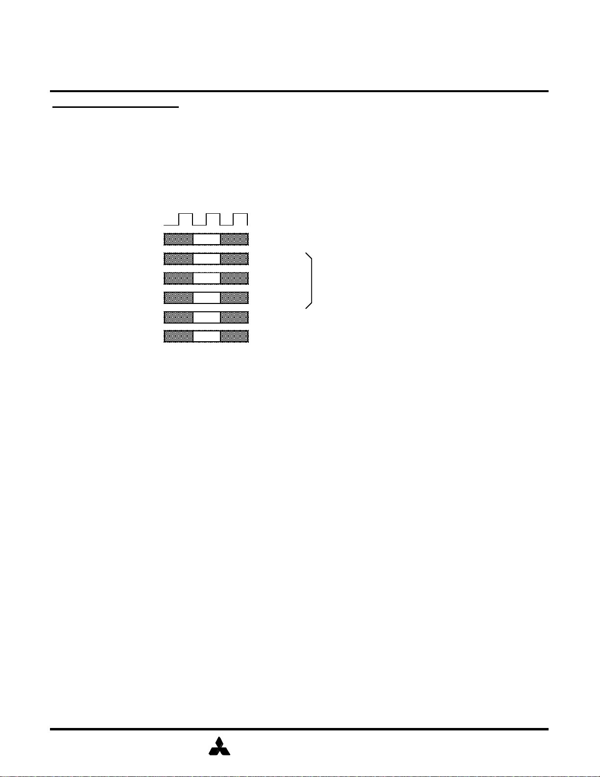
[ CAS LATENCY ]
/CAS latency, CL, is used to synchronize the first output data with the CLK frequency, i.e., the speed of
CLK determines which CL should be used. The DRAM column access, tCAC, determines the CL timing
requirements.
/CAS Latency Timing (BL=4)
CLK
Command
Address
DQ Q0 Q1 Q2 Q3
DQ Q0 Q1 Q2 Q3
DQ Q0 Q1 Q2 Q3
ACT
X
READ
tRCD
Y
CL=1
CL=2
CL=3
[ BURST LENGTH ]
The burst length, BL, determines the number of consecutive writes or reads that will be automatically
performed after the initial write or read command. For BL=1,2,4,8 the output data is tristated (Hi-Z) after
the last read. For BL=FP (Full Page) the TBST (Burst Terminate) command must be used to stop the output
of data.
tRCD
CLK
Command
Address
DQ
DQ
DQ
DQ Q0 Q1 Q2 Q3
DQ Q0 Q1 Q2 Q3
ACT
X
READ
Y
Q0
Q0 Q1
Q0 Q1 Q2 Q3
Burst Lengt h Timing (CL=2)
Q4 Q5 Q6 Q7
Q4 Q5 Q6 Q7 Q8 Q255 Q0 Q1
BL=1
BL=2
BL=4
BL=8
BL=FP
Full Page counter rolls over and continues to count.
MITSUBISHI ELECTRIC
13

SDRAM (Rev. 0.3)
MITSUBISHI LSIs
Feb ‘97 Preliminary
4M (2-BANK x 131072-WORD x 16-BIT) Synchronous DRAM
[ BURST ADDRESS SEQUENCE ]
CLK
Command
Address
DQ
CL= 3
BL= 4
Initial Address BL
A2 A1 A0
Read
Y
/CAS Latency Burst Length Burst Length
M5M4V4S40CTP-12, -15
Write
Y
Q0 Q1 Q2 Q3
Internal addresses ar e determ ined by B ur st Type.
Column Addressing / Burst Type
Sequential Interleaved
D0 D1 D2 D3
000
001
010
011
100
101
110
111
-00
-01
-10
-11
--0
--1
0123456701234567
1234567010325476
2345670123016745
3456701232107654
8
4567012345670123
5670123454761032
6701234567452301
7012
0123
1230
4
2301
30
01
2
10
3456 3210
12
7654
0123
1032
2301
32
01
10
10
Note: For FP Burst the Burst Type must be set to sequential.
MITSUBISHI ELECTRIC
14
 Loading...