

Mitsubishi M5M4V16G50DFP-8, M5M4V16G50DFP-12, M5M4V16G50DFP-10 Datasheet
M5M4V16G50DFP -8, -10, -12
Jan'97 Preliminary
MITSUBISHI LSIs
16M (2-BANK x 262144-WORD x 32-BIT) Synchronous Graphics RAM
MITSUBISHI ELECTRIC
SGRAM (Rev. 0.0)
DESCRIPTION
The M5M4V16G50DFP is a 2-bank x 262,144-word x 32-bit Synchronous GRAM,
with LVTTL interface. All inputs and outputs are referenced to the rising edge of
CLK. The M5M4V16G50DFP can operate at frequencies of 100+ MHz. The
BLOCK WRITE and WRITE-PER-BIT functions provide improved performance
in graphic memory systems.
FEATURES
- Single 3.3v±0.3v power supply
- Clock frequencies of 125 MHz
- Fully synchronous operation referenced to clock rising edge
- Dual bank operation controlled by A10(Bank Address)
- Internal pipelined operation: column address can be changed every clock cycle
- Programmable /CAS Latency (LVTTL: 2 and 3)
- Programmable Burst Length (1/2/4/8 and Full Page)
- Programmable Burst Type (Sequential / Interleave)
- Byte control using DQM0 - DQM3 signals in both read and write cycles
- Persistent Write-Per-Bit (WPB) function
- 8 Column Block Write (BW) function
- Auto Precharge / All bank precharge controlled by A9
- Auto Refresh and Self Refresh Capability
- 2048 refresh cycles /32ms
- LVTTL Interface
- 100 pin QFP package with 0.65mm lead pitch
Max.
Frequency
CLK Access
Time
M5M4V16G50DFP - 8 125MHz 7ns
M5M4V16G50DFP- 10 100MHz 8ns
PRELIMINARY
Some of contents are described for general products
and are subject to change without notice.
M5M4V16G50DFP- 12 83MHz 10ns
M5M4V16G50DFP -8, -10, -12
Jan'97 Preliminary
MITSUBISHI LSIs
16M (2-BANK x 262144-WORD x 32-BIT) Synchronous Graphics RAM
MITSUBISHI ELECTRIC
SGRAM (Rev. 0.0)
CLK : Master Clock
CKE : Clock Enable
/CS : Chip Select
/RAS : Row Address Strobe
/CAS : Column Address Strobe
/WE : Write Enable
DSF : Special Function Enable
A0-10 : Address Input
A0-9 : Row Address inputs
A0-7 : Column Address inputs
A10 : Bank Address
DQ0-31 : Data I/O
DQM0-3 : Output Disable/ Write Mask
Vdd : Power Supply
VddQ : Power Supply for Output
Vss : Ground
VssQ : Ground for Output
DQ29
VSSQ
DQ30
DQ31
VSS
NC
NC
NC
NC
NC
NC
NC
NC
NC
NC
VDD
DQ0
DQ1
VSSQ
DQ2
81
82
83
84
85
86
87
88
89
90
91
92
93
94
95
96
97
98
99
100
DQ28
VDDQ
807978
1
2
DQ27
4
3
DQ26
VSSQ
DQ25
777675
5
6
DQ24
VDDQ
747372
7891011
DQ15
DQ14
71
VSSQ
DQ13
70
696867
12
DQ12
VDDQ
VDD
VSS
DQ11
DQ10
65
64
66
636261605958575655
100 Pin QFP
14.0 x 20.0 mm2
0.65 mm pitch
14
13
15
16
17
18
VSSQ
VDDQ
DQ9
DQ8
19
202122232425262728
NC
DQM3
DQM1
CLK
DSFNCA9
CKE
29
51
50
49
48
47
46
45
44
43
42
41
40
39
38
37
36
35
34
33
32
31
30
545352
A7
A6
A5
A4
VSS
NC
NC
NC
NC
NC
NC
NC
NC
NC
NC
VDD
A3
A2
A1
A0
DQ3
VDDQ
DQ4
DQ5
VSSQ
DQ6
DQ7
VDDQ
DQ16
VSSQ
DQ17
DQ18
DQ19
VDDQ
VDD
VSS
DQ20
DQ21
VSSQ
DQ22
DQ23
VDDQ
DQM0
DQM2
/WE
/CAS
/RAS
/CS
A10
A8
M5M4V16G50DFP -8, -10, -12
Jan'97 Preliminary
MITSUBISHI LSIs
16M (2-BANK x 262144-WORD x 32-BIT) Synchronous Graphics RAM
MITSUBISHI ELECTRIC
SGRAM (Rev. 0.0)
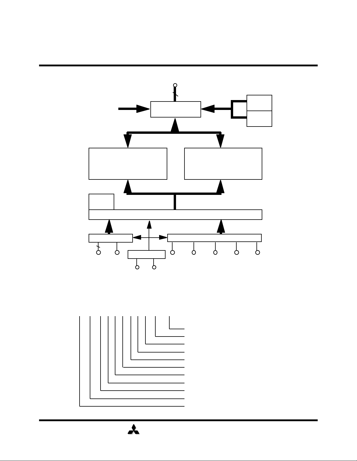
BLOCK DIAGRAM
DQM0-3
Memory Array
Bank #0
Mode
Register
Address Buffer
DQ0-31
I/O Buffer
Control Circuitry
Control Signal Buffer
Color
Register
Mask
Register
Memory Array
Bank #1
A0-9 A10
Clock Buffer
CLK CKE
Type Designation Code
M 5M 4 V 16 G 5 0 D FP - 8
/CS /RAS /CAS /WE DSF
This rule is applied only to Synchronous DRAM family.
Cycle Time (min.) 8: 8ns, 10: 10ns, 12: 12ns
Package Type FP: QFP
Process Generation
Function 0: Random Column, 1: 2N-rule
Organization 2n 5: x32
Synchronous Graphics RAM
Density 16:16M bits
Interface V:LVTTL
Memory Style (DRAM)
Use, Recommended Operating Conditions, etc
Mitsubishi Main Designation

M5M4V16G50DFP -8, -10, -12
Jan'97 Preliminary
MITSUBISHI LSIs
16M (2-BANK x 262144-WORD x 32-BIT) Synchronous Graphics RAM
MITSUBISHI ELECTRIC
SGRAM (Rev. 0.0)
PIN FUNCTION
CLK Input Master Clock: All other inputs are referenced to the rising edge of CLK.
CKE Input
Clock Enable: CKE controls internal clock. When CKE is low, internal clock
for the following cycle is stopped. CKE is also used to select auto / self
refresh. After self refresh mode is started, CKE becomes asynchronous
input. Self refresh is maintained as long as CKE is low.
/CS Input Chip Select: When /CS is high, any command means No Operation.
/RAS, /CAS, /
WE, and DSF
Input Combination of /RAS, /CAS, /WE, and DSF defines basic commands.
A0-9 Input
A0-9 specify the Row / Column Address in conjunction with BA. The Row
Address is specified by A0-9. The Column Address is specified by A0-7.
A9 is also used to indicate precharge option. When A9 is high at a read /
write command, an auto precharge is performed. When A9 is high at a
precharge command, both banks are precharged.
A10 Input
Bank Address: A10 (BA) specifies the bank to which a
command is applied. A10 (BA) must be set with ACT, PRE, READ,
WRITE commands.
DQ0-31 Input / Output
Data In/Data out are referenced to the rising edge of CLK. These pins
are used for input mask pins for Write-Per-Bit and column/byte mask
inputs for Block Writes.
DQM0 DQM3
Input
Input/Output Byte Mask: When DQM0-3 are high during a write, data for
the current cycle is masked. When DQM0-3 are high during a read,
output data is disabled at the next cycle.
DQM0 controls byte 0 (DQ7-0), DQM1 controls byte 1 (DQ15-8), DQM2
controls byte 2 (DQ23-16), and DQM3 controls byte 3 (DQ31-24).
VREF Input
Reference voltage for all inputs.
Vdd, Vss Power Supply Power Supply for the memory array and peripheral circuitry.
VddQ, VssQ Power Supply VddQ and VssQ are supplied to the Output Buffers only.
M5M4V16G50DFP -8, -10, -12
Jan'97 Preliminary
MITSUBISHI LSIs
16M (2-BANK x 262144-WORD x 32-BIT) Synchronous Graphics RAM
MITSUBISHI ELECTRIC
SGRAM (Rev. 0.0)
BASIC FUNCTIONS
The M5M4V16G50DFP provides basic functions, bank (row) activate, burst read / write, bank (row)
precharge, and auto / self refresh.
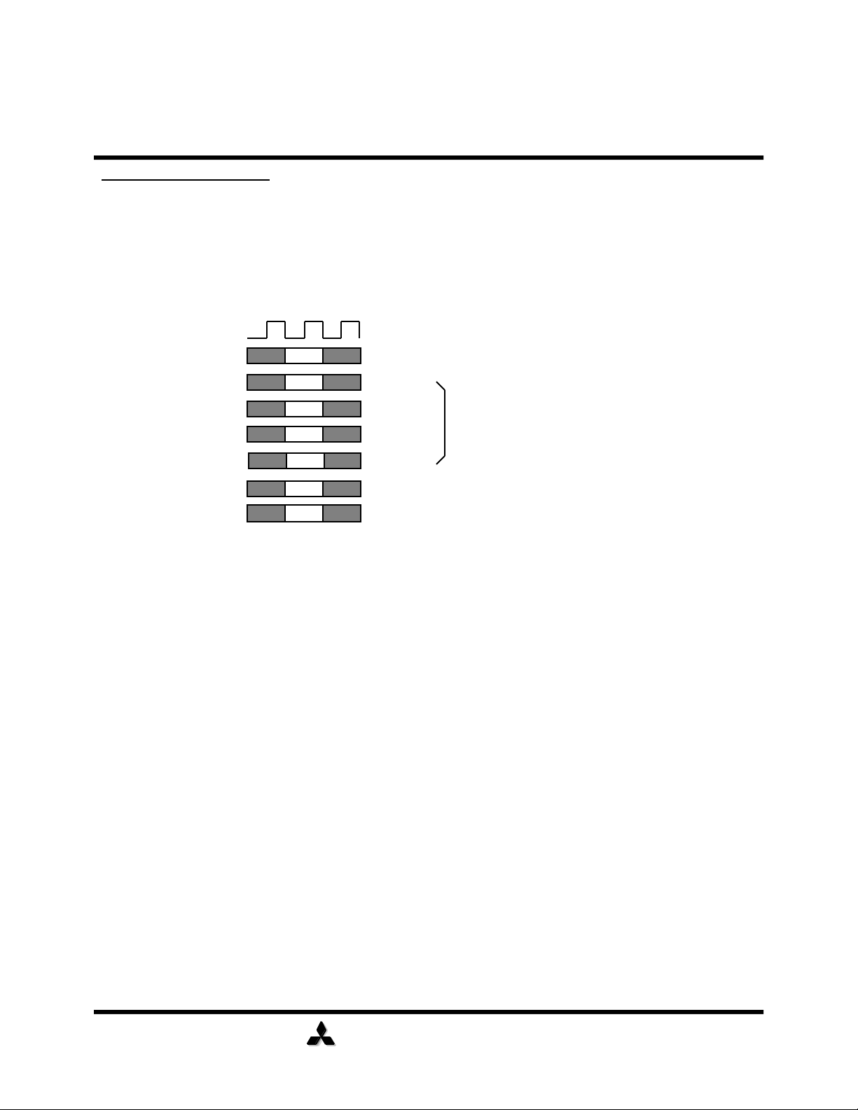
Each command is defined by control signals of /RAS, /CAS, /WE, and DSF at CLK rising edge. In
addition to 3 signals, /CS ,CKE and A9 are used as chip select, refresh option, and precharge option,
respectively.
For a more detailed definition of commands, please see the command truth table.
Activate (ACT) [/CS, /RAS, DSF = L, /CAS, /WE = H]
ACT command activates a row in an idle bank indicated by A10 (BA) and row address
selected by A0 - A9.
Activate with WPB enable (ACTWPB) [/CS, /RAS = L, /CAS, /WE, DSF = H]
This command is the same as Activate except that Write-Per-Bit (WPB) is enabled. The Mask
Register’s contents are used as the WPB data.
Read (READ) [/CS, /CAS, DSF = L, /RAS, /WE = H]
READ command starts burst read from the active bank indicated by A10 (BA). First output data
appears after /CAS latency. When A9 = H at this command, the bank is deactivated after the burst read
(auto-precharge, READA).
Write (WRITE) [/CS, /CAS, /WE, DSF = L, /RAS = H]
WRITE command starts burst write to the active bank indicated by A10 (BA). Total data length to be
written is set by burst length. When A9 = H at this command, the bank is deactivated after the burst
write (auto-precharge, WRITEA).
Precharge (PRE) [/CS, /RAS, /WE, DSF = L, /CAS = H]
PRE command deactivates the active bank indicated by A10 (BA). This command also terminates
burst read /write operation. When A9 = H at this command, both banks are deactivated
(precharge all, PREA).
/CS
Chip Select : L=select, H=deselect
/RAS
Command
/CAS
Command
/WE
Command
CKE
Refresh Option @refresh command
A9
Precharge Option @precharge or read/write command
CLK
define basic commands
DSF
Command

M5M4V16G50DFP -8, -10, -12
Jan'97 Preliminary
MITSUBISHI LSIs
16M (2-BANK x 262144-WORD x 32-BIT) Synchronous Graphics RAM
MITSUBISHI ELECTRIC
SGRAM (Rev. 0.0)
Auto-Refresh (REFA) [/CS, /RAS, /CAS, DSF = L, /WE, CKE = H]
REFA command starts auto-refresh cycle. Refresh address including bank address are generated internally. After this command, the banks are precharged automatically. Both banks must be precharged
before this command can begin.
Self-Refresh (REFS) [/CS, /RAS, /CAS, DSF, CKE = L, /WE = H]
REFS command starts self-refresh cycle. The self-refresh cycle will continue while CKE remains low.
When CKE goes high, self-refresh is exited. Refresh address including bank address are generated internally. After this command, the banks are precharged automatically. Both banks must be precharged
before this command can begin.
Burst Terminate (TERM) [/CS, /WE, DSF = L, /RAS, /CAS = H]
TERM command stops the current burst operation. During read cycles, burst data stops after CAS
latency is met.
No Operation (NOP) [/CS, DSF = L, /RAS, /CAS, /WE = H]
NOP command does not perform any operation on the SGRAM.
Mode Register Set (MRS) [/CS, /WE, /RAS, /CAS, DSF = L]
MRS command loads the mode register that defines how the device operates. The address pins, A0 A10, are used as input pins for the mode register data. This command must be issued after power-on to
initialize the SGRAM. The mode register can only be set when both banks are idle. During the two
cycles following this command, the SGRAM cannot accept any other commands.
Special Register Set (SRS) [/CS, /WE, /RAS, /CAS = L, DSF = H]
SRS command sets the color and mask registers. During the two cycles following this command, the
SGRAM cannot accept any other commands.
Masked Block Write (BW) [/CS, /CAS, /WE = L, /RAS, DSF = H]
BW command starts the 8 column Block Write function. Burst Length = 1 is assumed. Write data
comes from the color register and column address mask data is applied on the DQs. When A9 = H at
this command, the bank is deactivated after the burst write (auto-precharge, BWA).
BASIC FUNCTIONS (continued)
M5M4V16G50DFP -8, -10, -12
Jan'97 Preliminary
MITSUBISHI LSIs
16M (2-BANK x 262144-WORD x 32-BIT) Synchronous Graphics RAM
MITSUBISHI ELECTRIC
SGRAM (Rev. 0.0)
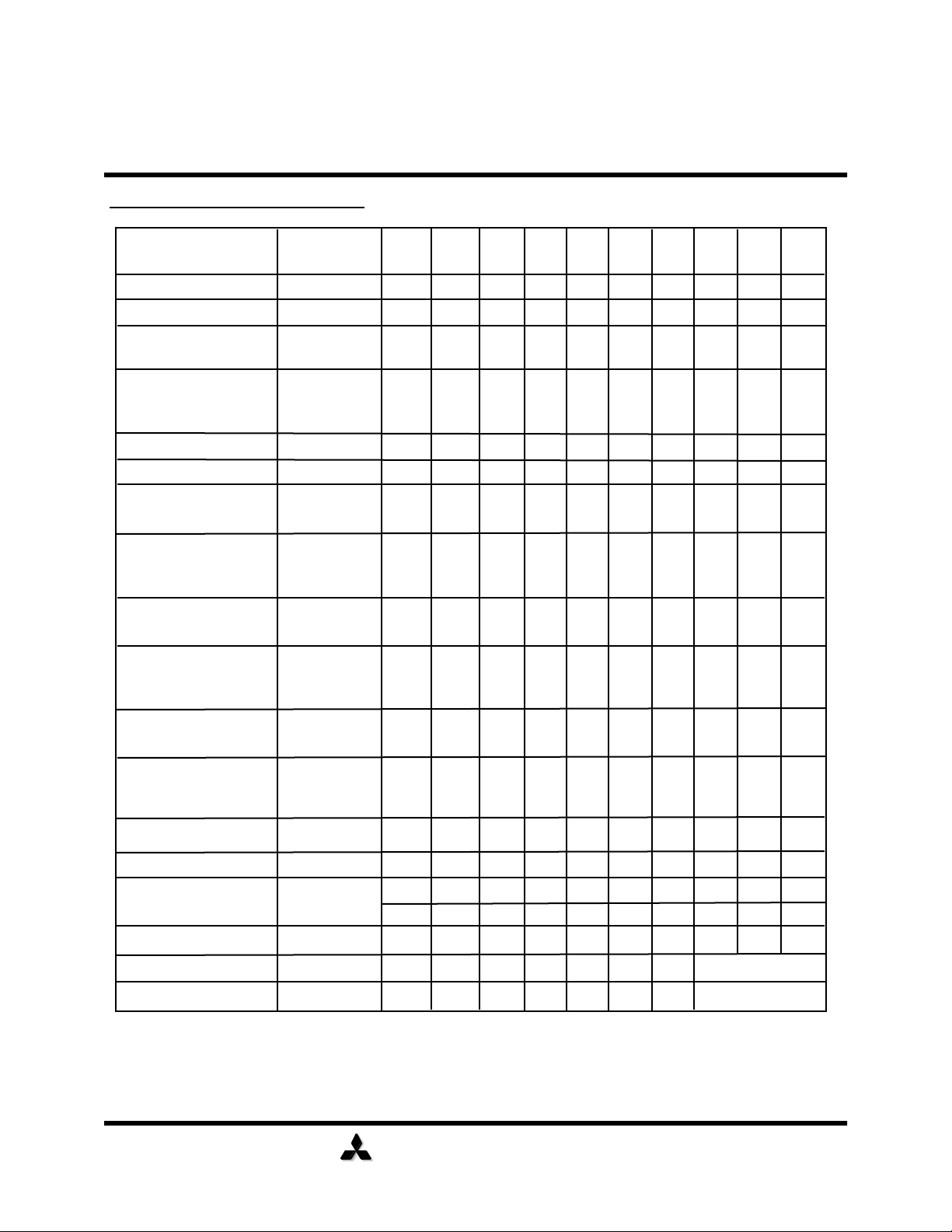
COMMAND TRUTH TABLE
H=High Level, L=Low Level, BA=Bank Address, Col.=Column Address (A0-A7)
Row Add.=Row Address (A0-A9), X=Don't Care, n=CLK cycle number
COMMAND MNEMONIC
CKE
n-1
CKE
n
/CS /RAS /CAS /WE A10 A9 A0-8
Deselect DESEL H X H X X X X X X
No Operation NOP H X L H H H X X X
Row Address Entry &
Bank Activate
ACT H X L L H H BA Row Add.
Single Bank Precharge PRE H X L L H L BA L X
Precharge All Banks PREA H X L L H L X H X
Column Address Entry
& Write
WRITE H X L H L L BA L Col.
Column Address Entry
& Write with Auto Precharge
WRITEA H X L H L L BA H Col.
Column Address Entry
& Read
READ H X L H L H BA L Col.
Column Address Entry
& Read with Auto Precharge
READA H X L H L H BA H Col.
Auto-Refresh REFA H H L L L H X X X
Self-Refresh Entry REFS H L L L L H X X X
Self-Refresh Exit REFSX
L H H X X X X X X
L H L H H H X X X
Burst Terminate TERM H X L H H L X X X
Mode Register Set MRS H X L L L L OPCODE
DSF
X
L
L
L
L
L
L
L
L
L
L
X
L
L
L
Special Register Set SRS H X L L L L
H
Row Address Entry &
Bank Activate
ACTWPB
H X L L H H BA Row Add.
H
Column Address Entry
& Masked Block Write
BW H X L H L L BA L Col.
Masked Block Write
with Auto-Precharge
BWA
H X L H L L BA H Col.
H
H
OPCODE
M5M4V16G50DFP -8, -10, -12
Jan'97 Preliminary
MITSUBISHI LSIs
16M (2-BANK x 262144-WORD x 32-BIT) Synchronous Graphics RAM
MITSUBISHI ELECTRIC
SGRAM (Rev. 0.0)
FUNCTION TRUTH TABLE
Current State
/CS /RAS /CAS /WE
Address Command Action
IDLE
H X X X
X DESEL NOP
L H H H
X NOP NOP
L H H L
X TERM ILLEGAL*2
L H L H
BA, CA, A9 READ / READA ILLEGAL*2
L L H H
BA, RA ACT Bank Active; Latch RA; No Mask
L L L H
X Undefined ILLEGAL
L L L H
X REFA Auto-Refresh*5
L L L L
Op-Code,
Mode-Add
SRS Special Register Set*5
ROW ACTIVE
H X X X
X DESEL NOP
L H H H
X NOP NOP
L H H L
BA TERM NOP
L H L H
BA, CA, A9 READ / READA
Begin Read; Latch CA;
Determine Auto-Precharge
L H L L
BA, CA, A9
WRITE /
WRITEA
Begin Write; Latch CA;
Determine Auto-Precharge
L L H H
BA, RA ACT Bank Active / ILLEGAL*2
L L H L
BA, A9 PRE / PREA Precharge / Precharge All
L L L H
X REFA ILLEGAL
L L L L
Op-Code,
Mode-Add
SRS Special RegisteSet *5
DSF
X
L
L
L
L
H
L
H
X
L
L
L
L
L
L
L
H
L H H L
X Undefined ILLEGAL
H
L H L H
X Undefined ILLEGAL
H
L H L L
BA, CA, A9 WRITE / WRITEA ILLEGAL*2
L
L H L L
BA, CA, A9 BW / BWA ILLEGAL*2
H
L L H H
BA, RA ACTWPB Bank Active; Latch RA; Use Mask
H
L L H L
X Undefined ILLEGAL
H
L L H L
BA, A9 PRE / PREA NOP*4
L
L L L L
Op-Code,
Mode-Add
MRS Mode Register Set*5
L
L L L L
Op-Code,
Mode-Add
MRS ILLEGAL
L
L L H H
BA, RA ACTWPB Bank Active / ILLEGAL*2
H
L H L L
BA, CA, A9
BW / BWA
Block Write; Latch CA;
Determine Auto-Precharge
H
M5M4V16G50DFP -8, -10, -12
Jan'97 Preliminary
MITSUBISHI LSIs
16M (2-BANK x 262144-WORD x 32-BIT) Synchronous Graphics RAM
MITSUBISHI ELECTRIC
SGRAM (Rev. 0.0)
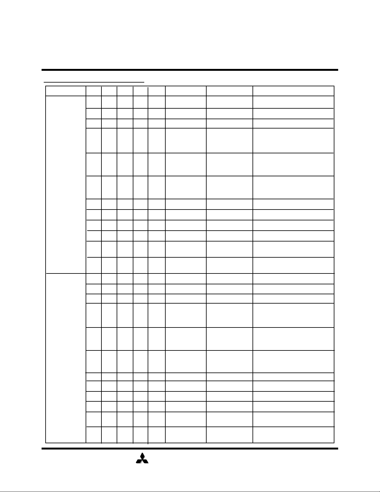
FUNCTION TRUTH TABLE
(continued)
Current State
/CS /RAS /CAS /WE
Address Command Action
READ
H X X X
X DESEL NOP (Continue Burst to END)
L H H H
X NOP NOP (Continue Burst to END)
L H H L
BA TERM Terminate Burst
L H L H
BA, CA, A9 READ / READA
Terminate Burst, Latch CA,
Begin New Read, Determine
Auto-Precharge*3
L H L L
BA, CA, A9
WRITE /
WRITEA
Terminate Burst, Latch CA,
Begin Write, Determine AutoPrecharge*3
L L H H
BA, RA ACT Bank Active / ILLEGAL*2
L L H L
BA, A9 PRE / PREA Terminate Burst, Precharge
L L L H
X REFA ILLEGAL
L L L L
Op-Code,
Mode-Add
SRS ILLEGAL
DSF
X
L
L
L
L
L
L
L
H
L H L L
BA, CA, A9
BW / BWA
Terminate Burst, Latch CA,
Block Write, Determine AutoPrecharge*3
H
L L H H
BA, RA
ACTWPB
Bank Active / ILLEGAL*2
L
L L L L
Op-Code,
Mode-Add
MRS ILLEGAL
L
WRITE
H X X X X DESEL NOP (Continue Burst to END)
L H H H X NOP NOP (Continue Burst to END)
L H H L BA TERM Terminate Burst
L H L H BA, CA, A9 READ / READA
Terminate Burst, Latch CA,
Begin Read, Determine AutoPrecharge*3
L H L L BA, CA, A89
WRITE /
WRITEA
Terminate Burst, Latch CA,
Begin Write, Determine AutoPrecharge*3
L L H H BA, RA ACT Bank Active / ILLEGAL*2
L L H L BA, A9 PRE / PREA Terminate Burst, Precharge
L L L H X REFA ILLEGAL
L L L L
SRS ILLEGAL
X
L
L
L
L
L
L
L
H
Op-Code,
Mode-Add
L L L L
MRS ILLEGAL
L
Op-Code,
Mode-Add
L H L L BA, CA, A9
BW / BWA
Terminate Burst, Latch CA,
Block Write, Determine AutoPrecharge*3
L
L L H H BA, RA ACTWPB Bank Active / ILLEGAL*2
L
M5M4V16G50DFP -8, -10, -12
Jan'97 Preliminary
MITSUBISHI LSIs
16M (2-BANK x 262144-WORD x 32-BIT) Synchronous Graphics RAM
MITSUBISHI ELECTRIC
SGRAM (Rev. 0.0)
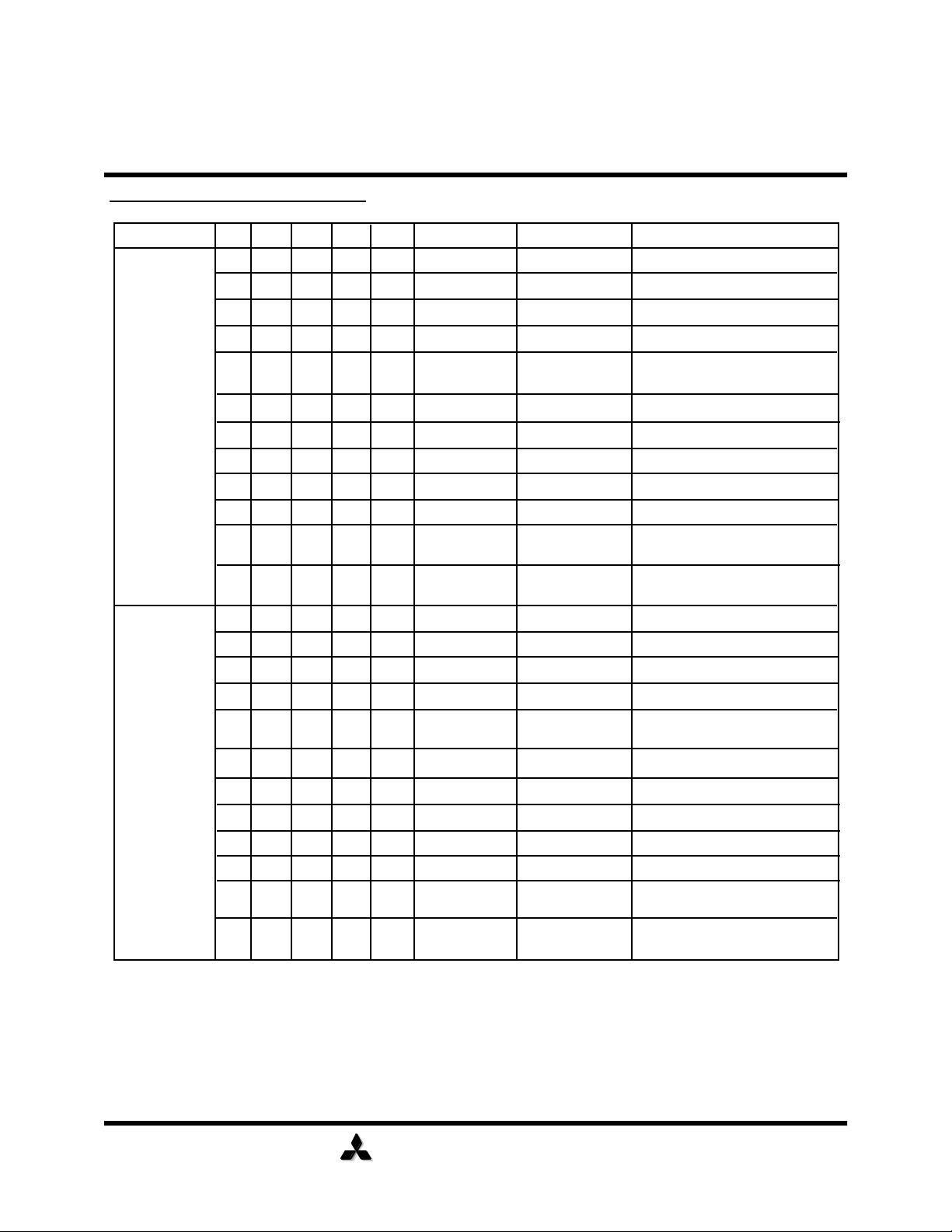
FUNCTION TRUTH TABLE
(continued)
Current State /CS /RAS /CAS /WE Address Command Action
READ with
AUTO
PRECHARGE
H X X X X DESEL NOP (Continue Burst to END)
L H H H X NOP NOP (Continue Burst to END)
L H H L BA TERM ILLEGAL
L H L H BA, CA, A9 READ / READA ILLEGAL
L H L L BA, CA, A9
WRITE /
WRITEA
ILLEGAL
L L H H BA, RA ACTWPB Bank Active / ILLEGAL*2
L L H L BA, A9 PRE / PREA ILLEGAL*2
L L L H X REFA ILLEGAL
L L L L
Op-Code,
Mode-Add
SRS ILLEGAL
WRITE with
AUTO
PRECHARGE
H X X X X DESEL NOP (Continue Burst to END)
L H H H X NOP NOP (Continue Burst to END)
L H H L BA TERM ILLEGAL
L H L H BA, CA, A9 READ / READA ILLEGAL
L H L L BA, CA, A9
WRITE /
WRITEA
ILLEGAL
L L H H BA, RA ACTWPB Bank Active / ILLEGAL*2
L L H L BA, A9 PRE / PREA ILLEGAL*2
L L L H X REFA ILLEGAL
L L L L
Op-Code,
Mode-Add
SRS ILLEGAL
DSF
X
L
L
L
L
H
L
L
H
X
L
L
L
L
H
L
L
H
L H L L BA, CA, A9
BW / BWA
ILLEGAL
H
L L H H BA, RA ACT Bank Active / ILLEGAL*2
L
L L L L
Op-Code,
Mode-Add
MRS ILLEGAL
L
L L L L
Op-Code,
Mode-Add
MRS ILLEGAL
L
L H L L BA, CA, A9
BW / BWA
ILLEGAL
H
L L H H BA, RA ACT Bank Active / ILLEGAL*2
L
 Loading...