

Mitsubishi M5M29FT800FP-12, M5M29FT800FP-10, M5M29FT800FP, M5M29FB800VP-80, M5M29FB800VP-12 Datasheet
...
MITSUBISHI LSIs
M5M29FB/T800FP,VP,RV-80,-10,-12
May 1997 , Rev.6.1
8,388,608-BIT (1048,576-WORD BY 8-BIT / 524,288-WORD BY16-BIT)
CMOS 3.3V-ONLY, BLOCK ERASE FLASH MEMORY
1
MITSUBISHI LSIs
DESCRIPTION
The MITSUBISHI M5M29FB/T800FP, VP, RV are 3.3V-only high speed 8,388,608-bit CMOS boot block Flash Memories suitable for
mobile and personal computing, and communication products. The M5M29FB/T800FP, VP, RV are fabricated by CMOS technology for
the peripheral circuits and DINOR(Divided bit line NOR) architecture for the memory cells, and are available in 44pin SOP or 48pin
TSOP(I).
FEATURES
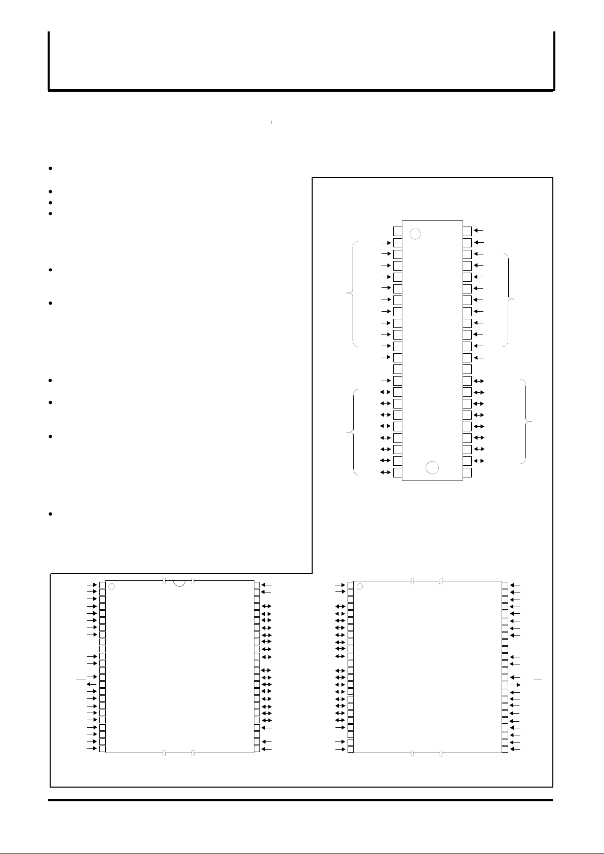
PIN CONFIGURATION (TOP VIEW)
Organization 524,288 word x 16bit
1,048,576 word x 8 bit
Supply voltage ................................ VCC = 3.3V±0.3V
Access time 80/100/120ns (Max)
Power Dissipation
Read 108 mW (Max.)
Program/Erase 144 mW (Max.)
Standby 0.72 mW (Max.)
Deep power down mode 3.3µW (typ.)
Auto program
Program Time 7.5ms (typ.)
Program Unit 128word
Auto Erase
Erase time 50 ms (typ.)
Erase Unit
Boot Block 8Kword / 16Kbyte x 1
Parameter Block 4Kword / 8Kbyte x 2
Main Block 16Kword / 32Kbyte x 1
32Kword / 64Kbyte x 15
Program/Erase cycles 100Kcycles
Boot Block
M5M29FB800 Bottom Boot
M5M29FT800 Top Boot
Other Functions
Software Command Control
Selective Block Lock
Erase Suspend/Resume
Program Suspend/Resume
Status Register Read
Sleep
Package
48-Lead, 12mmx 20mm TSOP (type-I)
44-Lead SOP
8,388,608-BIT (1048,576-WORD BY 8-BIT / 524,288-WORD BY16-BIT)
CMOS 3.3V-ONLY, BLOCK ERASE FLASH MEMORY
M5M29FB/T800FP,VP,RV-80,-10,-12
1
NC : NO CONNECTION
RV(Reverse bend): 48P3R-COutline 48pin TSOP type-I (12 X 20mm)
VP(Normal bend): 48P3R-B
This product is compatible with HN29WB/T800 by Hitachi Ltd.
1
2
3
4
5
6
7
8
9
10
44
43
42
41
40
38
37
35
11
12
34
33
39
36
13 32
14
31
15 30
16 29
M5M29FB/T800FP
17 28
18 27
19 26
20 25
Outline 600mil 44-pin SOP
(FP: 44P2A-A)
21 24
22
23
.................................
..............................
.......................
.......................
.......................
.................................
.................................
........................
.............................
.................................
...........................
.................................
.......................
.......................
.......................
A15
A12
A10
DQ5
DQ12
A8
A13
A14
DQ4
/WE
A9
VCC
GND
A16
/RP
DQ13
A11
DQ6
DQ7
DQ14
DQ15/A-1
/BYTE/CE
A7
A5
A4
DQ0
DQ1
DQ2
DQ3
A3
A2
A1
A17
A18
DQ11
DQ10
DQ9
DQ8
/OE
GND
A0
A6
ADDRESS
INPUTS
ADDRESS
INPUTS
CHIP ENABLE
INPUT
BYTE ENABLE
INPUT
RESET/
POWER DOWN
INPUT
WRITE ENABLE
INPUT
DATA
INPUTS/
OUTPUTS
DATA
INPUTS/
OUTPUTS
OUTPUT ENABLE
INPUT
1
2
3
4
5
6
7
8
9
10
11
12
13
14
15
16
44
43
42
41
40
39
38
37
36
35
34
33
32
31
30
29
A18
A17
A16
RY/BY
NC
A11
A10
M5M29FB/T800VP
A15
/CE
17
18
19
20
28
27
26
25
DQ0
A0
21
22
23
24
48
47
46
45
A13
A12
A14
GND
/OE
A9
A8
NC
NC
/RP
A7
A6
A5
A4
A1
A2
A3
/WE
/BYTE
DQ8
DQ1
DQ9
DQ2
VCC
GND
DQ10
DQ3
DQ11
DQ4
DQ12
DQ5
DQ13
DQ6
DQ14
DQ7
DQ15/A-1
/WP
APPLICATION
Code Storage PC BIOS
Digital Cellular Phone/Telecommunication
1
2
3
4
5
6
7
8
9
10
11
12
13
14
15
16
44
43
42
41
40
39
38
37
36
35
34
33
32
31
30
29
RY/BY
M5M29FB/T800RV
A15
17
18
19
20
28
27
26
25
21
22
23
24
48
47
46
45
A14
GND
A18
A17
A7
A6
A5
A4
A1
A2
A3
NC
/RP
A11
A10
A9
A8
NC
NC
A13
A12
/WE
/CE
DQ0
A0
/OE
DQ8
DQ1
DQ9
DQ2
/WP
VCC
GND
DQ10
DQ3
DQ11
DQ4
DQ12
DQ5
DQ13
DQ6
DQ14
DQ7
DQ15/A-1
A16
/BYTE
NC
...........................
...........................
.......................................
MITSUBISHI LSIs
M5M29FB/T800FP,VP,RV-80,-10,-12
May 1997 , Rev.6.1
8,388,608-BIT (1048,576-WORD BY 8-BIT / 524,288-WORD BY16-BIT)
CMOS 3.3V-ONLY, BLOCK ERASE FLASH MEMORY
2
FUNCTION
BLOCK DIAGRAM
Deep Power-Down
When /RP is at VIL, the device is in the deep powerdown
mode and its power consumption is substantially low. During
read modes, the memory is deselected and the data
input/output are in a high-impedance(High-Z) state. After
return from powerdown, the CUI is reset to Read Array , and
the Status Register is cleared to value 80H.
During block erase or program modes, /RP low will abort
either operation. Memory array data of the block being altered
become invalid.
X-DECODER
Y-DECODER
Y-GATE / SENSE AMP.
INPUT/OUTPUT
BUFFERS
/CE
/OE
/WE
VCC (3.3V)
GND (0V)
DATA INPUTS/OUTPUTS
The M5M29FB/T800FP,VP,RV includes on-chip program/erase
control circuitry. The Write State Machine (WSM) controls block
erase and page program operations. Operational modes are
selected by the commands written to the Command User Interface
(CUI). The Status Register indicates the status of the WSM and
when the WSM successfully completes the desired program or
block erase operation.
A Deep Powerdown mode is enabled when the /RP pin is at GND,
minimizing power consumption.
Read
The M5M29FB/T800FP,VP,RV has three read modes, which
accesses to the memory array, the Device Identifier and the Status
Register. The appropriate read command are required to be
written to the CUI. Upon initial device powerup or after exit from
deep powerdown, the M5M29FB/T800 automatically resets to read
array mode. In the read array mode, low level input to /CE and
/OE, high level input to /WE and /RP, and address signals to the
address inputs (A0-A18) output the data of the addressed location
to the data input/output(D0-15).
Write
Writes to the CUI enables reading of memory array data, device
identifiers and reading and clearing of the Status Register. They
also enable block erase and program. The CUI is written by
bringing /WE to low level, while /CE is at low level and /OE is at
high level. Address and data are latched on the earlier rising edge
of /WE and /CE. Standard micro-processor write timings are used.
D15/A-1D14D13D12
D2 D1
D0
D3
/WP
/RP
MULTIPLEXER
CUI WSM
STATUS / ID REGISTER
128 WORD PAGE BUFFER
Main Block 32KW
Standby
When /CE is at VIH, the device is in the standby mode and its
power consumption is reduced. Data input/output are in a
high-impedance(High-Z) state. If the memory is deselected during
block erase or program, the internal control circuits remain active
and the device consume normal active power until the operation
completes.
RY/BY
READY/BUSY OUTPUT
A18
A17
A16
A15
A14
A13
A12
A11
A10
A9
A8
A7
A6
A5
A4
A3
A2
A1
A0
Main Block 32KW
Main Block 16KW
Parameter Block2 4KW
Parameter Block1 4KW
Boot Block 8KW
ADDRESS
INPUTS
/BYTE
CHIP ENABLE INPUT
OUTPUT ENABLE INPUT
WRITE ENABLE INPUT
WRITE PROTECT INPUT
RESET/POWER DOWN INPUT
BYTE ENABLE INPUT
Output Disable
When /OE is at VIH, output from the devices is disabled.
Data input/output are in a high-impedance(High-Z) state.

MITSUBISHI LSIs
M5M29FB/T800FP,VP,RV-80,-10,-12
May 1997 , Rev.6.1
8,388,608-BIT (1048,576-WORD BY 8-BIT / 524,288-WORD BY16-BIT)
CMOS 3.3V-ONLY, BLOCK ERASE FLASH MEMORY
3
SOFTWARE COMMAND DEFINITIONS
The device operations are selected by writing specific software
command into the Command User Interface.
Read Array Command (FFH)
The device is in Read Array mode on initial device powerup and
after exit from deep powerdown, or by writing FFH to the
Command User Interface. The device remains in Read Array
mode until the other commands are written.
Read Device Identifier Command (90H)
Though PROM programmers can normally read device identifier
codes by raising A9 to VID, multiplexing high voltage onto address
lines is not desired for micro-processor system. It is an other
means to read device identifier codes that Read Device Identifier
Code Command(90H) is written to the command latch. Following
the command write, the manufacturer code and the device code
can be read from address 0000H and 0001H, respectively.
Read Status Register Command (70H)
The Status Register is read after writing the Read Status Register
command of 70H to the Command User Interface.
The contents of Status Register are latched on the later falling
edge of /OE or /CE. So /CE or /OE must be toggled every status
read.
Clear Status Register Command (50H)
The Erase Status and Program Status bits are set to "1"s by the
Write State Machine and can only be reset by the Clear Status
Register command of 50H. These bits indicates various failure
conditions.
DATA PROTECTION
The M5M29FB/T800 provides selectable block locking of memory
blocks. Each block has an associated nonvolatile lock-bit which
determines the lock status of the block. In addition, the
M5M29FB/T800 has a master Write Protect pin (WP) which
prevents any modifications to memory blocks whose lock-bits are
set to "0", when /WP is low. When /WP is high or /RP is VHH, all
blocks can be programmed or erased regardless of the state of
the lock-bits, and the lock-bits are cleared to "1" by erase.
Power Supply Voltage
When the power supply voltage (Vcc) is less than 2.2V, the device
is set to the Read-only mode.
A delay time of 2 us is required before any device operation is
initiated. The delay time is measured from the time Vcc reaches
Vccmin (3.0V).
During power up, /RP=GND is recommended. Falling in Busy
status is not recommended for possibility of damaging the device.
Block Erase / Confirm Command (20H/D0H)
Automated block erase is initiated by writing the Block Erase
command of 20H followed by the Confirm command of D0H. An
address within the block to be erased is required. The WSM
executes iterative erase pulse application and erase verify
operation.
Page Program Commands(41H)
Page Program allows fast programming of 128words of data.
Writing of 41H initiates the page program operation. From 2nd
cycle to 129th cycle write data must be serially inputted. Address
A6-0 have to be incremented from 00H to 7FH. After completion
of data loading, the WSM controls the program pulse application
and verify operation.
Basically re-program must not be done on a page which has
already programmed.
Suspend/Resume Command (B0H/D0H)
Writing the Suspend command of B0H during block erase
operation interrupts the block erase operation and allows read out
from another block of memory. Writing the Suspend command of
B0H during program operation interrupts the program operation
and allows read out from another block of memory. The device
continues to output Status Register data when read, after the
Suspend command is written to it. Polling the WSM Status and
Suspend Status bits will determine when the erase operation or
program operation has been suspended. At this point, writing of
the Read Array command to the CUI enables reading data from
blocks other than that which is suspended. When the Resume
command of D0H is written to the CUI, the WSM will continue with
the erase or program processes.
MITSUBISHI LSIs
M5M29FB/T800FP,VP,RV-80,-10,-12
May 1997 , Rev.6.1
8,388,608-BIT (1048,576-WORD BY 8-BIT / 524,288-WORD BY16-BIT)
CMOS 3.3V-ONLY, BLOCK ERASE FLASH MEMORY
4
1) X at RY/BY is VOL or VOH(Hi-Z).
*The RY/BY is an open drain output pin and indicates status of the internal WSM. When low,it indicates that the WSM is Busy performing an operation.
A pull-up resistor of 10K-100K Ohms is required to allow the RY/BY signal to transition high indicating a Ready WSM condition.
2) X can be VIH or VIL for control pins.
BUS OPERATIONS
32Kword MAIN BLOCK
32Kword MAIN BLOCK
32Kword MAIN BLOCK
32Kword MAIN BLOCK
32Kword MAIN BLOCK
32Kword MAIN BLOCK
32Kword MAIN BLOCK
32Kword MAIN BLOCK
32Kword MAIN BLOCK
32Kword MAIN BLOCK
32Kword MAIN BLOCK
32Kword MAIN BLOCK
32Kword MAIN BLOCK
32Kword MAIN BLOCK
32Kword MAIN BLOCK
16Kword MAIN BLOCK
4Kword PARAMETER BLOCK
4Kword PARAMETER BLOCK
8Kword BOOT BLOCK
M5M29FB800 Memory Map
8Kword BOOT BLOCK
32Kword MAIN BLOCK
32Kword MAIN BLOCK
32Kword MAIN BLOCK
32Kword MAIN BLOCK
32Kword MAIN BLOCK
32Kword MAIN BLOCK
32Kword MAIN BLOCK
32Kword MAIN BLOCK
32Kword MAIN BLOCK
32Kword MAIN BLOCK
32Kword MAIN BLOCK
32Kword MAIN BLOCK
32Kword MAIN BLOCK
32Kword MAIN BLOCK
16Kword MAIN BLOCK
4Kword PARAMETER BLOCK
4Kword PARAMETER BLOCK
32Kword MAIN BLOCK
M5M29FT800 Memory Map
78000H-7FFFFH
70000H-77FFFH
68000H-6FFFFH
60000H-67FFFH
58000H-5FFFFH
50000H-57FFFH
48000H-4FFFFH
40000H-47FFFH
38000H-3FFFFH
30000H-37FFFH
28000H-2FFFFH
20000H-27FFFH
18000H-1FFFFH
10000H-17FFFH
08000H-0FFFFH
04000H-07FFFH
03000H-03FFFH
02000H-02FFFH
00000H-01FFFH
F0000H-FFFFFH
E0000H-EFFFFH
D0000H-DFFFFH
C0000H-CFFFFH
B0000H-BFFFFH
A0000H-AFFFFH
90000H-9FFFFH
80000H-8FFFFH
70000H-7FFFFH
60000H-6FFFFH
50000H-5FFFFH
40000H-4FFFFH
30000H-3FFFFH
20000H-2FFFFH
10000H-1FFFFH
08000H-0FFFFH
06000H-07FFFH
04000H-05FFFH
00000H-03FFFH
A-1-A18(Bytemode)A0-A18(Wordmode)
7E000H-7FFFFH
7D000H-7DFFFH
7C000H-7CFFFH
78000H-7BFFFH
70000H-77FFFH
68000H-6FFFFH
60000H-67FFFH
58000H-5FFFFH
50000H-57FFFH
48000H-4FFFFH
40000H-47FFFH
38000H-3FFFFH
30000H-37FFFH
28000H-2FFFFH
20000H-27FFFH
18000H-1FFFFH
10000H-17FFFH
08000H-0FFFFH
00000H-07FFFH
FC000H-FFFFFH
FA000H-FBFFFH
F8000H-F9FFFH
F0000H-F7FFFH
E0000H-EFFFFH
D0000H-DFFFFH
C0000H-CFFFFH
B0000H-BFFFFH
A0000H-AFFFFH
90000H-9FFFFH
80000H-8FFFFH
70000H-7FFFFH
60000H-6FFFFH
50000H-5FFFFH
40000H-4FFFFH
30000H-3FFFFH
20000H-2FFFFH
10000H-1FFFFH
00000H-0FFFFH
A-1-A18(Bytemode)A0-A18(Wordmode)
x8 ( Bytemode) x16 ( Wordmode) x8 ( Bytemode) x16 ( Wordmode)
1)
Mode
Array
Status Register
Identifier Code
Stand by
Program
Erase
Write
Read
Pins
/CE /OE /WE
VIL
VIL
VIL
VIL
VIH
VIL
VIL
VIL
VIL
VIL
VIH
X
VIH
VIH
VIH
VIH
VIH
VIH
X
VIL
VIL
Data out
Status Register Data
Identifier Code
Hi-Z
Hi-Z
Command/Data in
Command
Output disable
Deep Power Down
Others
/RP
VIH
VIH
VIH
VIH
VIH
VIH
VIH
RY/BY
VOH (Hi-Z)
X
X
X
X
X
X
VIL VIH
X
VIL
X Hi-Z
VIH
VIL
XCommand
Bus Operations for Word-Wide Mode (/BYTE=VIH)
DQ0-15
2)
VIH
Lock Bit Status VIL VIL
VIH
Lock Bit Data (DQ6) X
VOH (Hi-Z)
VOH (Hi-Z)
1)
Mode
Array
Status Register
Identifier Code
Stand by
Program
Erase
Write
Read
Pins
/CE /OE /WE
DQ0-7
VIL
VIL
VIL
VIL
VIH
VIL
VIL
VIL
VIL
VIL
VIH
X
VIH
VIH
VIH
VIH
VIH
VIH
X
VIL
VIL
Data out
Status Register Data
Identifier Code
Hi-Z
Hi-Z
Command/Data in
Command
Output disable
Deep Power Down
Others
/RP
VIH
VIH
VIH
VIH
VIH
VIH
VIH
RY/BY
X
X
X
X
X
X
VIL
VIH
X
VIL
X Hi-Z
VIH
VIL
X
Command
Bus Operations for Byte-Wide Mode (BYTE=VIL)
2)
Lock Bit Status
VIL VIL
VIH
VIH
Lock Bit Data (DQ6)
X
VOH (Hi-Z)
VOH (Hi-Z)
VOH (Hi-Z)
MITSUBISHI LSIs
M5M29FB/T800FP,VP,RV-80,-10,-12
May 1997 , Rev.6.1
8,388,608-BIT (1048,576-WORD BY 8-BIT / 524,288-WORD BY16-BIT)
CMOS 3.3V-ONLY, BLOCK ERASE FLASH MEMORY
5
BLOCK LOCKING
D6 provides Lock Status of each block after writing the Read Lock Status command (71H).
In case of TSOP package, /WP pin must not be switched during performing Read / Write operations or WSM Busy (WSMS = 0).
/RP
/WP Lock Bit(Internally)
VIL
VHH
VIH
VIH
VIH
X
X
VIL
VIL
VIH
X
X
X
0
1
Write Protection Provided
All Blocks Locked (Deep Power Down Mode)
Blocks Locked (Depend on Lock Bit Data)
All Blocks UnLocked
Blocks Unlocked (Depend on Lock Bit Data)
All Blocks Unlocked
STATUS REGISTER
Status
Erase Status
Program Status
Definition
Symbol
(D5)
(D4)
Write State Machine Status
(D7)
(D6)
Reserved
(D1)
(D0)
(D3)
Reserved(D2)
"1" "0"
Ready Busy
Suspended Operation in Progress / Completed
Error Successful
Error Successful
- -
- -
SR.5
SR.4
SR.7
SR.6
SR.1
SR.0
SR.3
SR.2
Block Status after Program
Device Sleep Status
Device in Sleep
Suspend Status
DEVICE IDENTIFIER CODE
Code
Manufacturer Code
Pins
Hex. Data
1CH
D0
0
A0
VIL
D1
0
D2
1
D3
1
D4
1
D5
0
D6
0
D7
0
Device Code (-T)
5DH0VIH
1
1 1
1
0
1
0
Device Code (-B)
5EH
0VIH 11
1
10
1
0
In the word-wide mode, the same data as D7-0 is read out from D15-8.
A9 = VHH Mode : A9 = 11.5V~13.0V Set A9 to VHH min.200ns before falling edge of /CE in ready status. Min.200ns after return to VIH ,device can't be accessed.
A1~A8, A10~A18, /CE,/OE = VIL, /WE = VIH
D15/A-1 = VIL (/BYTE = L)
*The RY/BY is an open drain output pin and indicates status of the internal WSM. When low,it indicates that the WSM is Busy performing an operation.
A pull-up resistor of 10K-100K Ohms is required to allow the RY/BY signal to transition high indicating a Ready WSM condition.
Error Successful
Device Not in Sleep
*D3 indicates the block status after the page programming. When D3 is "1", the page has the over-programed cell . If over-program occures, the device is block
fail. However if D3 is "1", please try the block erase to the block. The block may revive.
SOFTWARE COMMAND DEFINITION
Command List
Read Array
FFHXWrite
3rd bus cycle1st bus cycle 2nd bus cycle
Command
AddressMode Data AddressMode Data AddressMode Data
Device Identifier
90H
XWrite
ID
IARead
Read Status Register
70HXWrite SRDXRead
Clear Status Register
50H
XWrite
Page Program XWrite
WD0
Write41H
XWrite
WA0
Write
WD1WA1Write
Block Erase / Confirm
20H
XWrite
D0H
BA
Write
Suspend
B0H
XWrite
Resume
71H
XWrite
2)
3)
5)
6)
4)
Read Lock Bit Status
Lock Bit Program / Confirm
Erase All Unlocked Blocks
Write
Write
X
X A7H
77H
D0H
Write
Read
BA
BA
X D0H
D0H
DQ6
2)
(D7-0)(D7-0)(D7-0)
1) In the word-wide mode, upper byte data (D8-D15) is ignored.
2) IA=ID Code Address : A0=VIL (Manufacturer's Code) : A0=VIH (Device Code), ID=ID Code,
/BYTE =VIL : A-1, A1-A18 = VIL, /BYTE =VIH : A1-A18 = VIL
3) SRD = Status Register Data
4) WA=Write Address, WD=Write Data.
/BYTE =VIL : Write Address and Write Data must be provided sequentially from 00H to FFH for A-1-A6.
Page size is 256Byte (256byte x 8bit), /BYTE =VIH : Write Address and Write Data must be provided
sequentially from 00H to 7FH for A0-A6. Page size is 128word (128word x 16bit).
5) BA = Block Address ( Addresses except Block Address mest be VIH.)
6) DQ6 provides Block Lock Status, DQ6 = 1 : Block Unlock, DQ6 = 0 : Block Locked.
7) Sleep command (F0H) put the device into the sleep mode after completing the current operation. The active current is reduced to deep power -down levels.
The Read Array command (FFH) must be written to get the device out of sleep mode.
4)
4)
Sleep
Write
X F0H
7)
/RP
VIL
VHH
VIH
VIH
Lock Bit(Internally)
X
X
0
1
SOP Package
TSOP Package

MITSUBISHI LSIs
M5M29FB/T800FP,VP,RV-80,-10,-12
May 1997 , Rev.6.1
8,388,608-BIT (1048,576-WORD BY 8-BIT / 524,288-WORD BY16-BIT)
CMOS 3.3V-ONLY, BLOCK ERASE FLASH MEMORY
6
CAPACITANCE
Symbol
Parameter
Test conditions
pF
pF
Unit
Max
8
12
Typ
Min
Limits
Ta = 25°C, f = 1MHz, Vin = Vout = 0V
Input capacitance (Address, Control Pins)
Output capacitance
CIN
COUT
Conditions
ABSOLUTE MAXIMUM RATINGS
Parameter
With respect to Ground
Symbol
Vcc
All input or output voltage except Vcc,A9,/RP
VI1
Vcc voltage
1)
Unit
V
V
Min Max
4.6-0.2
-0.6
14.0
Ambient temperature
Temperature under bias
Ta
Tbs
Storage temperature
Tstg
°C
°C
°C
0 70
-10 80
-65 125
Output short circuit currentI OUT mA
100
VI2 A9,RP supply voltage
-0.6 4.6
V
1) Minimum DC voltage is -0.5V on input/output pins. During transitions, this level may undershoot to -2.0V for periods <20ns. Maximum DC voltage
on input/output pins is VCC+0.5V which, during transitions, may overshoot to VCC+1.5V for periods <20ns.
DC ELECTRICAL CHARACTERISTICS (Ta = 0 ~ 70°C, Vcc = 3.3V±0.3V, unless otherwise noted)
Symbol Parameter
MaxTyp1)
Limits
Min
Test conditions Unit
VCC standby current
ILO
±10
Output leakage current µA
0V≤VOUT≤VCC
ILI Input leakage current µA
0V≤VIN≤VCC ±1.0
VCC deep powerdown current
Output high voltage
V
VOL Output low voltage VIOL = 5.8mA 0.45
Vcc+0.5
VIH Input high voltage V2.0
0.8VIL Input low voltage – 0.5
VOH1 IOH = –2.5mA 0.85Vcc V
VOH2 IOH = –100µA
Vcc–0.4
V
All currents are in RMS unless otherwise noted.
1) Typical values at Vcc=3.3V, Ta=25°C
2) To protect against initiation of write cycle during Vcc power-up/ down, a write cycle is locked out for Vcc less than VLKO.
If Vcc is less than VLKO, Write State Machine is reset to read mode. When the Write State Machine is in Busy state, if Vcc is less than VLKO, the alteration of memory contents
may occur.
ICC3 VCC program current mA40VCC = 3.6V, VIN=VIL/VIH, /CE = /RP =/WP = VIH
ICC4 VCC erase current mA40VCC = 3.6V, VIN=VIL/VIH, /CE = /RP =/WP = VIH
VID A9 intelligent identifier voltage 11.4 12.6 V12.0
VIHH 11.4 12.6 V/RP
unlock voltage
12.0
VLKO Low VCC Lock-Out voltage 2) 1.5 2.5 V
I
RP
/RP
all block unlock current /RP = VHH max 100 µA
IID A9 intelligent identifier current A9 = VID max 100 µA
ICC5 VCC suspend current 200VCC = 3.6V, VIN=VIL/VIH, /CE = /RP =/WP = VIH µA
ISB2 5
VCC = 3.6V, VIN=GND or VCC,
/CE = /RP = /WP= VCC±0.3V
µA1
25 mAICC1 VCC read current for Word or Byte
VCC = 3.6V, VIN=VIL/VIH, /CE = VIL,
/RP=OE=VIH, f = 10MHz, IOUT = 0mA
7
ISB1 VCC = 3.6V, VIN=VIL/VIH, /CE = /RP =/WP = VIH µA20050
ICC2 30 mAVCC Write current for Word or Byte
VCC = 3.6V,VIN=VIL/VIH, /CE =/WE= VIL,
/RP=/OE=VIH
VCC = 3.6V, VIN=VIL/VIH, /RP = VIL µA155ISB3
µA1ISB4
VCC = 3.6V, VIN=GND or VCC, /RP =GND±0.3V
5

MITSUBISHI LSIs
M5M29FB/T800FP,VP,RV-80,-10,-12
May 1997 , Rev.6.1
8,388,608-BIT (1048,576-WORD BY 8-BIT / 524,288-WORD BY16-BIT)
CMOS 3.3V-ONLY, BLOCK ERASE FLASH MEMORY
7
Read-Only Mode
AC ELECTRICAL CHARACTERISTICS (Ta = 0 ~70°C, Vcc = 3.3±0.3V)
Write Mode (/WE control)
AC ELECTRICAL CHARACTERISTICS (Ta = 0 ~ 70°C, Vcc = 3.3V±0.3V)
Symbol
Parameter
Unit
MaxMinMaxMin
Limits
M5M29FB/T800-10 M5M29FB/T800-12
Timing measurements are made under AC waveforms for read operations.
TypTyp
Read timing parameters during command write operations mode are the same as during read-only operations mode.
Typical values at Vcc=3.3V, Ta=25°C
MaxMin
M5M29FB/T800-80
ta (AD) Address access time ns100 120tAVQV 80
tCLZ Chip enable to output in low-Z ns0 0tELQX 0
ta (CE) Chip enable access time ns100 120tELQV 80
ta (OE) Output enable access time ns50 60tGLQV 40
tDF(CE) Chip enable high to output in high Z ns25 30tEHQZ 25
tRC Read cycle time ns100 120tAVAV 80
/BYTE low to output high-Z ns3025tBHZ tFLQZ 25
Typ
tWHGL /OE hold from /WE high
tOEH
/CE low to /BYTE high or lowtBCD ns5 5tELFL/H 5
ns100 12080
ns0 00tOH Output hold from /CE, /OE, addressestOH
/BYTE access time ns120100ta(BYTE) 80tFL/HQV
tOLZ ns0 0tGLQX 0Output enable to output in low-Z
tDF(OE) nstGHQZ Output enable high to output in high Z 25 3025
tPHZ /RP low to output high-Z nstPLQZ 150 300150
tBAD nsAddress to /BYTE high or lowtAVFL/H 5 55
/RP recovery to /CE low ns
tPS
tPHEL 500500500
Symbol
Parameter
Unit
MaxMinMaxMin
Limits
M5M29FB/T800-10 M5M29FB/T800-12
Typ TypMaxMin
M5M29FB/T800-80
tWC tAVAV Write cycle time ns100 12080
tDH tWHDX Data hold time ns
tDS tDVWH Data set-up time ns50 5050
tAH tWHAX Address hold time ns
10
tAS tAVWH Address set-up time ns50 5050
tWP tWLWH Write pulse width ns60 6060
tCH tWHEH Chip enable hold time ns
tCS tELWL Chip enable set-up time ns0 00
tWPH tWHWL Write pulse width high ns20 2020
tPS tPHWL /RP high recovery to write enable low ns500 500500
tBLS
tBLH
Block Lockhold from valid SRD ns0 0tQVPH 0
tWHRL tWHRL Write enable high to RY/BY low ns100 12080
tDAP tWHRH1 Duration of auto-program operation ms7.5 120 1207.57.5 120
tDAE tWHRH2 Duration of auto-block erase operation 50 600 50 600 ms50 600
Typ
Block Lock set-up to write enable high ns100 120tPHHWH 80
tWPH
tBS tFL/HWH Byte enable high or low set-up time ns50 5050
tBH tWHFL/H Byte enable high or low hold time ns100 12080
tWPS
10
10 10
10 10
0 0 0

MITSUBISHI LSIs
M5M29FB/T800FP,VP,RV-80,-10,-12
May 1997 , Rev.6.1
8,388,608-BIT (1048,576-WORD BY 8-BIT / 524,288-WORD BY16-BIT)
CMOS 3.3V-ONLY, BLOCK ERASE FLASH MEMORY
8
Write Mode (/CE control)
AC ELECTRICAL CHARACTERISTICS (Ta = 0 ~ 70°C, Vcc = 3.3V±0.3V)
Read timing parameters during command write operations mode are the same as during read-only operations mode.
Typical values at Vcc=3.3V, Ta=25°C
Erase and Program Performance
Block Erase Time
Main Block Write Time (Page Mode)
Page Write Time
Parameter
ms
sec
ms
UnitTyp
7.5
1.9
50
Max
120
3.8
600
Min
Vcc Power Up / Down Timing
Symbol UnitTyp
2
MaxMin
tVCS
Parameter
/RP =VIH set-up time from Vccmin µs
During power up/down, by the noise pulses on control pins, the device has possibility of accidental erasure or programming.
The device must be protected against initiation of write cycle for memory contens during power up/down.
The delay time of min.2µsec is always required before read operation or write operation is initiated from the time Vcc reaches
Vccmin during power up/down. By holding /RP VIL, the contens of memory is protected during Vcc power up/down.
During power up, /RP must be held VIL for min.2µs from the time Vcc reaches Vccmin.
During power down, /RP must be held VIL until Vcc reaches GND.
/RP doesn't have latch mode ,so /RP must be held VIH during read operation or erase/program operation.
Symbol Parameter
Unit
MaxMinMaxMin
Limits
M5M29FB/T800-10 M5M29FB/T800-12
Typ TypMaxMin
M5M29FB/T800-80
tWC tAVAV Write cycle time ns100 12080
tDH tEHDX Data hold time ns
tDS tDVEH Data set-up time ns50 5050
tAH tEHAX Address hold time ns
tAS tAVEH Address set-up time ns50 5050
tCEP tELEH /CE pulse width ns60 6060
tWH tEHWH Write enable hold time ns0 00
tWS tWLEL Write enable set-up time ns0 00
tCEPH tEHEL /CE pulse width high ns20 2020
tPS tPHEL /RP high recovery to write enable low ns500 500500
tBLS
tBLH
Block Lockhold from valid SRD ns0 0tQVPH 0
tEHRL tEHRL
/CE enable high to RY/BY low
ns100 12080
tDAP tEHRH1 Duration of auto-program operation ms7.5 120 1207.57.5 120
tDAE tEHRH2 Duration of auto-block erase operation 50 600 50 600 ms50 600
Typ
Block Lock set-up to write enable high ns100 120tPHHEH 80
tWPH
tBS tFL/HEH Byte enable high or low set-up time ns50 5050
tBH tEHFL/H Byte enable high or low hold time ns100 12080
tWPS
10
10
10
10
10
10

MITSUBISHI LSIs
M5M29FB/T800FP,VP,RV-80,-10,-12
May 1997 , Rev.6.1
8,388,608-BIT (1048,576-WORD BY 8-BIT / 524,288-WORD BY16-BIT)
CMOS 3.3V-ONLY, BLOCK ERASE FLASH MEMORY
9
TEST CONDITIONS
FOR AC CHARACTERISTICS
Input voltage : VIL = 0V, VIH = 3.0V
Input rise and fall times : ≤5ns (80ns)
≤10ns (100/120ns)
Reference voltage
at timing measurement : 1.5V
Output load : 1TTL gate +
CL(100pF for 100/120ns)
CL(30pF for 80ns)
or
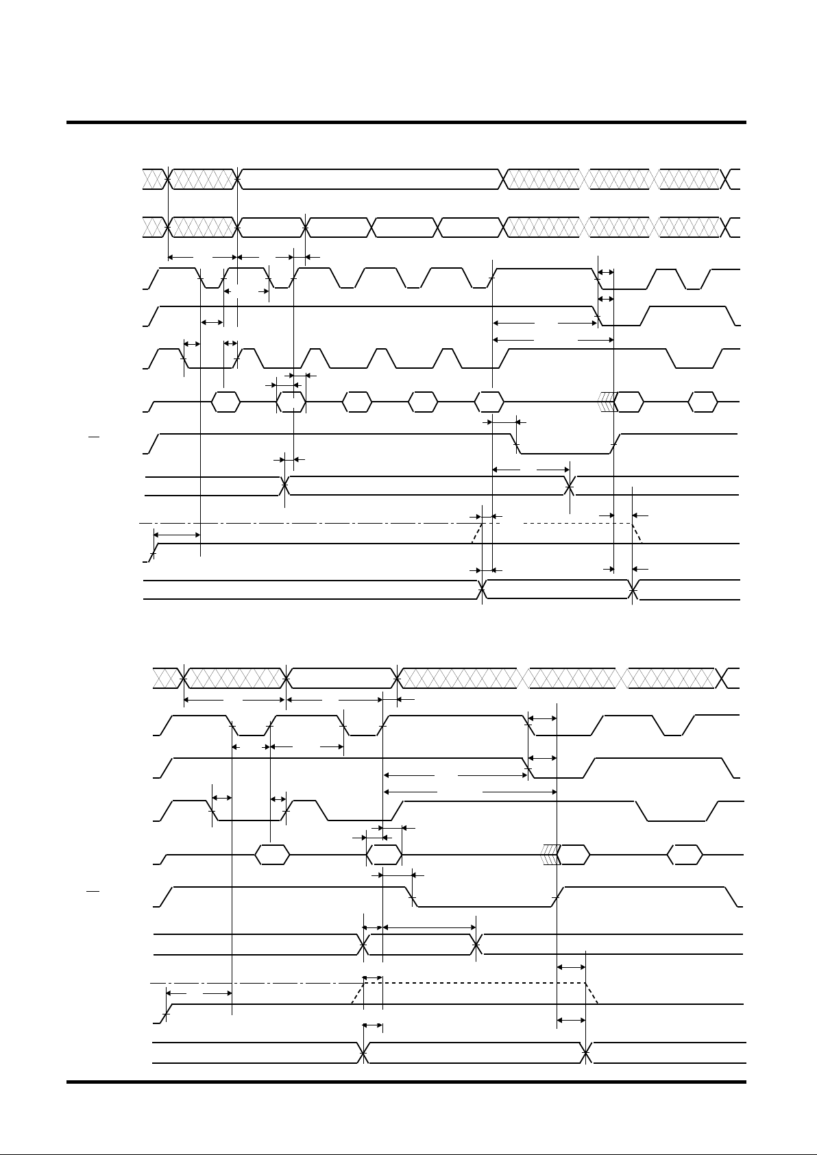
AC WAVEFORMS FOR READ OPERATION AND TEST CONDITIONS
OUTPUT VALID
HIGH-Z
tDF(OE)
tRC
VIH
VIL
VIH
VIL
VIH
VIL
VIH
VIL
VOH
VOL
ADDRESSES
/CE
/OE
/WE
DATA
ADDRESS VALID
3.3V
GND
VCC
tOH
tOLZ
ta (CE)
tOEH
tCLZ
ta (AD)
ta (OE)
HIGH-Z
DUT
3.3kΩ
1N914
1.3V
CL =30/100pF
VIH
VIL
/RP
tPS
VIH
VIL
VIH
VIL
VIH
VIL
VIH
VIL
ADDRESSES
(A0 - A18)
ADDRESS VALID
/CE
/BYTE
DATA
(D0 - D7)
BYTE AC WAVEFORMS FOR READ OPERATION
ta(AD)
HIGH-Z
VIH
VIL
DATA
(D8 - D14)
HIGH-Z
VIH
VIL
D15 / A-1
ta(BYTE)
tBHZ
VALID
VALID
OUTPUT VALID
VALID
A-1D15
A-1
VIH
VIL
/OE
When /BYTE=VIH, /CE=/OE=VIL , D15/A-1 is output status. At this time, input signal must not be applied.
ADDRESS VALID
ta(AD)
ta(CE)
ta(OE)
ta(BYTE)
tBCD
tBAD
tCLZ
tOLZ
tBAD
tOH
tDF(OE)
tDF(CE)
tDF(CE)
tPHZ
Vcc POWER UP / DOWN TIMING
VIH
VIL
/RP
Read /Write Inhibit
tVCS
VIH
VIL
/CE
VIH
VIL
/WE
tPS
tPS
Read /Write Inhibit
Read /Write Inhibit

MITSUBISHI LSIs
M5M29FB/T800FP,VP,RV-80,-10,-12
May 1997 , Rev.6.1
8,388,608-BIT (1048,576-WORD BY 8-BIT / 524,288-WORD BY16-BIT)
CMOS 3.3V-ONLY, BLOCK ERASE FLASH MEMORY
10
AC WAVEFORMS FOR ERASE OPERATIONS (/WE control)
41H DIN
tWPH
tWP
tDS
tDH
tCS tCH
tWC
VIH
VIL
VIH
VIL
VIH
VIL
VIH
VIL
A7~A18
ADDRESS VALID
/CE
/OE
/WE
DATA
RY/BY
tAH
VIH
/BYTE
VOH
VOL
VIL
/BYTE=VIL
(A-1~A6)
00H
01H FFH
02H~FEH
tAS
DIN DIN
SRD
DIN
VIH
VIL
tOEH
tDAE,tDAP
tWHRL
PROGRAM
READ STATUS
REGISTER
WRITE READ
ARRAY COMMAND
AC WAVEFORMS FOR PAGE PROGRAM OPERATION (/WE control)
FFH
tPS
VIH
VIL
/RP
VIH
VIL
/WP
tWPH
tWPS
VHH
20H D0H
tWPH
tWP
tDS
tDH
tCS tCH
tWC
VIH
VIL
VIH
VIL
VIH
VIL
VIH
VIL
RY/BY
tAH
VIH
VOH
VOL
VIL
ADDRESSES
tAS
FFHSRD
tOEH
tDAP,tDAE
tWHRL
ADDRESS VALID
ERASE
READ STATUS
REGISTER
WRITE READ
ARRAY COMMAND
VIL
VIH
VIL
tPS
VIH
/BYTE
/CE
/OE
/WE
DATA
/RP
/WP
tBLS
tBLH
VHH
/BYTE=VIH
(A0 ~A6)
7FH
02H~7EH
01H
00H
ta(CE)
ta(OE)
tBLH
tBLS
VIH
VIL
tBS
tBH
ta(OE)
ta(CE)
tWPS
tWPH
VIH
VIL
tBS
tBH
MITSUBISHI LSIs
M5M29FB/T800FP,VP,RV-80,-10,-12
May 1997 , Rev.6.1
8,388,608-BIT (1048,576-WORD BY 8-BIT / 524,288-WORD BY16-BIT)
CMOS 3.3V-ONLY, BLOCK ERASE FLASH MEMORY
AC WAVEFORMS FOR ERASE OPERATIONS (/CE control)
AC WAVEFORMS FOR PAGE PROGRAM OPERATION (/CE control)
11
41H DIN
tCEPH
tCEP
tDS
tDH
tWS tWH
tWC
VIH
VIL
VIH
VIL
VIH
VIL
VIH
VIL
A7~A18
ADDRESS VALID
/CE
/OE
/WE
DATA
RY/BY
tAH
VIH
/BYTE
VOH
VOL
VIL
/BYTE=VIL
(A-1~A6)
00H
01H FFH
02H~FEH
tAS
DIN DIN SRDDIN
VIH
VIL
tOEH
tDAE,tDAP
tEHRL
PROGRAM
READ STATUS
REGISTER
WRITE READ
ARRAY COMMAND
FFH
tPS
VIH
VIL
/RP
VIH
VIL
/WP
tWPH
tWPS
VHH
/BYTE=VIH
(A0 ~A6)
7FH
02H~7EH
01H
00H
ta(CE)
ta(OE)
tBLH
tBLS
VIH
VIL
tBS
tBH
20H D0H
tCEPH
tCEP
tDS
tDH
tWS
tWH
tWC
VIH
VIL
VIH
VIL
VIH
VIL
VIH
VIL
RY/BY
tAH
VIH
VOH
VOL
VIL
ADDRESSES
tAS
FFHSRD
tOEH
tDAP,tDAE
tEHRL
ADDRESS VALID
ERASE
READ STATUS
REGISTER
WRITE READ
ARRAY COMMAND
VIL
VIH
VIL
tPS
VIH
/BYTE
/CE
/OE
/WE
DATA
/RP
/WP
tBLS
tBLH
VHH
ta(OE)
ta(CE)
tWPS
tWPH
VIH
VIL
tBS
tBH
MITSUBISHI LSIs
M5M29FB/T800FP,VP,RV-80,-10,-12
May 1997 , Rev.6.1
8,388,608-BIT (1048,576-WORD BY 8-BIT / 524,288-WORD BY16-BIT)
CMOS 3.3V-ONLY, BLOCK ERASE FLASH MEMORY
12
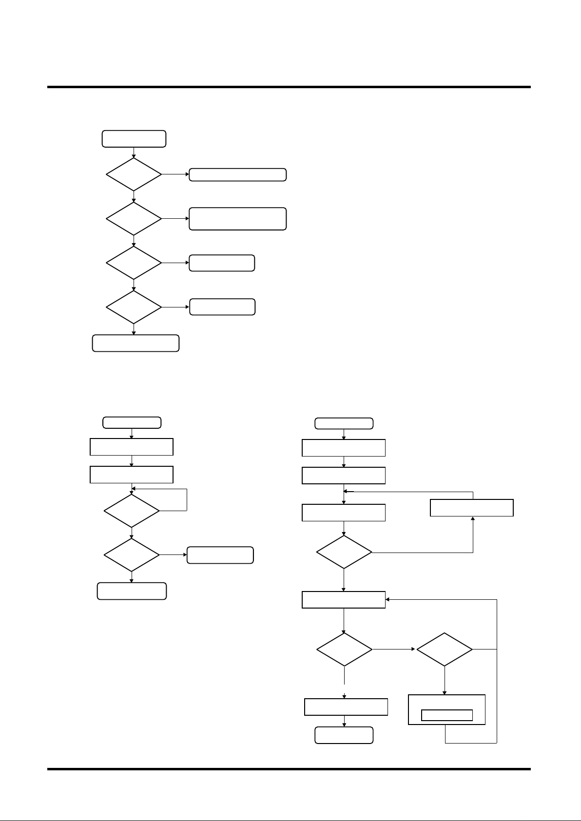
FULL STATUS CHECK PROCEDURE
SR.5 = 0 ?
SR.4 = 0 ?
SR.4 =1
and
SR.5 =1
?
SUCCESSFUL
(BLOCK ERASE, PROGRAM)
YES
YES
YES
NO
STATUS REGISTER
READ
COMMAND SEQUENCE ERROR
NO
BLOCK ERASE ERROR
NO
PROGRAM ERROR
(BLOCK)
WRITE 77H
WRITE D0H
BLOCK ADDRESS
LOCK BIT PROGRAM FLOW CHART
SR.4 = 0 ?
LOCK BIT PROGRAM
SUCCESSFUL
YES
YES
NO
NO
START
LOCK BIT PROGRAM
FAILED
SR.7 = 1 ?
SR.3 = 0 ?
YES
NO
PROGRAM ERROR
(PAGE, LOCK BIT)
PAGE PROGRAM FLOW CHART
START
WRITE 41H
FULL STATUS CHECK
IF DESIRED
PAGE PROGRAM
COMPLETED
YES
n = 0
n = n+1
WRITE
ADDRESS n, DATA n
YES
SR.7 = 1 ?
n = FFH ?
or
n = 7FH ?
NO
WRITE B0H ?
YES
NO
SUSPEND LOOP
WRITE D0H
YES
NO
STATUS REGISTER
READ

MITSUBISHI LSIs
M5M29FB/T800FP,VP,RV-80,-10,-12
May 1997 , Rev.6.1
8,388,608-BIT (1048,576-WORD BY 8-BIT / 524,288-WORD BY16-BIT)
CMOS 3.3V-ONLY, BLOCK ERASE FLASH MEMORY
13
SUSPEND / RESUME FLOW CHART
START
WRITE B0H
OPERATION
RESUMED
SR.6 =1?
YES
NO
WRITE FFH
READ ARRAY DATA
DONE
READING ?
NO
YES
WRITE D0H
SUSPEND
RESUME
BLOCK ERASE FLOW CHART
START
WRITE 20H
WRITE D0H
BLOCK ADDRESS
FULL STATUS CHECK
IF DESIRED
YES
SR.7 = 1 ?
WRITE B0H ?
YES
NO
SUSPEND LOOP
WRITE D0H
YES
NO
STATUS REGISTER
READ
BLOCK ERASE
COMPLETED
STATUS REGISTER
READ
SR.7 = 1?
YES
NO
PROGRAM / ERASE
COMPLETED

MITSUBISHI LSIs
M5M29FB/T800FP,VP,RV-80,-10,-12
May 1997 , Rev.6.1
8,388,608-BIT (1048,576-WORD BY 8-BIT / 524,288-WORD BY16-BIT)
CMOS 3.3V-ONLY, BLOCK ERASE FLASH MEMORY
14
OPERATION STATUS and EFFECTIVE COMMAND
Page Program
Setup
Lock Bit Program
Setup
Block Erase
Setup
F0H
Setup State
Internal State
Sleep State
Read/Standby State
[Sleep]
OTHER
Erase &
Verify
Read
Status Register
request
Sleep
F0H
return
B0H
D0H
B0H D0H
READY
IS REQUEST SLEEP?
Y
N
50H
41H
77H
20H
A7H
Suspend State
Read Array
Read
Status Register
Read
Device Identifier
Read
Lock Status
FFH
70H
90H
70H
90H
FFH
FFH
71H
70H
90H 71H
90H
invalid data
Read
Status Register
Read
Device Identifier
Read
Lock Status
FFH
70H
90H
70H
90H
FFH
FFH
71H
70H
71H
90H
Read Array
Read
Status Register
70H
90H
FFH
[Wake Up / Read Array]
OTHER OTHER
D0HD0H
D0H
WDi
i=0-255
Read
Device Identifier
Erase All Unlocked
Blocks Setup
Program &
Verify
Read
Status Register
request
Sleep
F0H
return
71H
71H
50H
FFH
FFH
FFH
Clear
Status Register
Read
Lock Status
71H
71H
70H
90H
 Loading...