

Page 1

Diamond View LCD Monitor
DV172 / DV172B (B=Black Cosmetic)
Service Guide
February 2003
Distributed by
Mitsubishi Electric Australia Pty. Ltd.
A.B.N. 58 001 215 792
348 Victoria Road
RYDALMERE NSW 2116
Australia
Telephone 1300 605 808
Page 2

Copyright
Copyright ã 1996 by the Company. All rights reserved. No part of this publication may be
reproduced, transmitted, transcribed, stored in a retrieval system, or translated into any language or
computer language, in any form or by any means, electronic, mechanical, magnetic, optical,
chemical, manual or otherwise, without the prior written permission of the Company.
Disclaimer
The Company makes no representations or warranties, either expressed or implied, with respect to
the contents hereof and specifically disclaims any warranties, merchantability or fitness for any
particular purpose. Further, the Company reserves the right to reserve this publication and to make
changes from time to time in the contents hereof without obligation of the Company to notify any
person of such revision or changes.
ii
Page 3

Section
Diamond View LCD Monitor
DV172 / DV172B
(B = Black Cosmetic’s)
Manual Contents
1. Engineering Specifications
2. Circuit Operation Theory
3. Alignment procedure
4. Trouble Shooting
5. Parts Lists (DV172 & DV172B)
6. Schematic Diagrams
7. Assembly
iii
Page 4

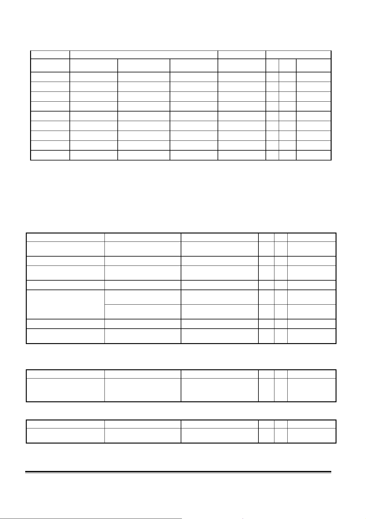
DV172 LCD Monitor Service Guide
Engineering Specification
Table of Contents
1. INTRODUCTION ...................................................................................................................................2
2. ELECTRICAL CHARACTERISTICS.................................................................................................3
OWER SUPPLY
2.1 P
IGNAL INTERFACE
2.2 S
IDEO PERFORMANCE
2.3 V
2.4 SCAN RANGE.........................................................................................................................................5
2.5 PLUG & PLAY DDC2B SUPPORT ..........................................................................................................5
UPPORT TIMINGS
2.6 S
3. OPERATIONAL & FUNCTIONAL SPECIFICATION.....................................................................6
3.1 VIDEO PERFORMANCE...........................................................................................................................6
3.2 BRIGHTNESS ADJUSTABLE RANGE........................................................................................................6
3.3 ACOUSTICAL NOISE ..............................................................................................................................6
3.4 AUDIO PERFORMANCE ..........................................................................................................................7
4. LCD CHARACTERISTICS...................................................................................................................7
......................................................................................................................................3
...............................................................................................................................3
...........................................................................................................................5
.................................................................................................................................5
4.1 THE PHYSICAL DEFINITION & TECHNOLOGY SUMMARY OF LCD PAN EL ...............................................7
5. USER CONTROLS.................................................................................................................................8
5.1 USER’S HARDWARE CONTROL DEFINITION: ...........................................................................................8
5.2 OSD CONTROL FUNCTION DEFINITION..................................................................................................8
6. MECHANICAL CHARACTERISTICS...............................................................................................9
6.1 DIMENSION ...........................................................................................................................................9
EIGHT
6.2 W
................................................................................................................................................9
6.3 PLASTIC ................................................................................................................................................9
6.4 CARTON ................................................................................................................................................9
7. CERTIFICATION...................................................................................................................................9
APPENDIX: PHYSICAL DIMENSION FRONT VIEW AND SIDE VIEW......................................11
1
Page 5
DV172 LCD Monitor Service Guide
Engineering Specification
1. Introduction
This specification describes DV172, a 17.0” dual interface color TFT LCD monitor with speakers
supported. The display supports up to 1280x1024/75Hz resolution & refresh rate and 262144 colors with
dithering. The features summary is as below,
Feature items Specifications Remark
Panel supplier & Panel type of supplier AUO M170EN05 TN with Film type
Actual Size Diagonal display 17.0" Panel display size
Actual Resolution display SXGA(1280x1024) Panel display resolution
+/- 70 degrees Horizontal (typ.)
+/- 70 degrees Vertical (typ.)
+/- 60 degrees Horizontal (min.)
Viewing Angle (at Contrast Ratio ≧ 10)
Analog interface with Scaling supported
DVI interface with Scaling supported
Video interface with Scaling supported No N.A.
Max resolution mode supported 1280 x 1024 at 75Hz
Number of Display Colors supported 262144 (with dithering) Panel driver is 6 bit
Contrast Ratio 250:1 (min.), 500:1 (typ.)
Luminance
AC power input
DC power input(with AC power adapter) No N.A.
DPMS supported
LED indicator for power status showed
OSD for control & information supported
Multi-language supported for OSD
Buttons control supported
Flywheel control supported No N.A.
Scaling function supported
Auto adjustment function supported
DDC function supported(EDID ver. 1.3)
Audio speakers supported
Audio Jack(input connector) supported
Earphone Jack(input connector) supported No N.A.
Microphone function supported No N.A.
Mechanical Tilt base design
VESA wall mounting design
Mechanical Rotate design No N.A.
Mechanical Lift base design No N.A.
+/- 60 degrees Vertical (min.) Panel spec
Yes
Yes
200 cd/m2 (min.),
260 cd/m2 (typ.)
Yes
Yes
Yes
Yes
Yes
Yes
Yes
Yes
Yes
Yes
Yes
Yes
Yes
With 15 pin D-sub connector
With 24 pin DVI connector.
At R,G,B saturated condition
(Default “User” color setting)
90-264 Volts, 47-63 Hz.
< 3 watts
Green/Amber/Non
6 languages
6 buttons including 1 monitor
power on/off control button.
Genesis gm5120
“Auto” key function
DDC2B only
From 0 to +20 degree
2
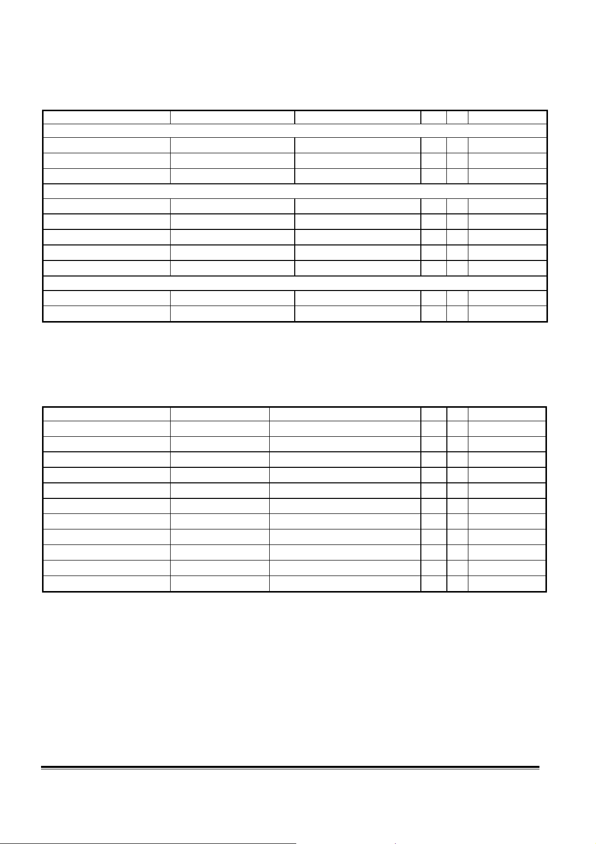
Page 6
DV172 LCD Monitor Service Guide
2. Electrical Characteristics
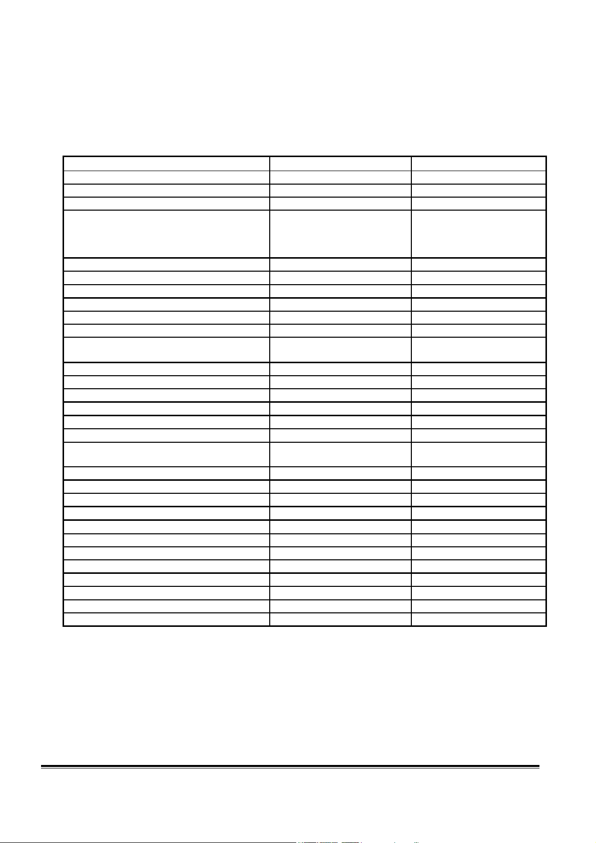
2.1 Power supply
Item Condition Spec OK N.A Remark
Input Voltage range
Input Current range
Power Consumption
DPMS
Inrush Current
Earth Leakage Current
Hi-Pot
Power Line Transient
CCFL operation range
CCFL Frequency
Power cord
2.2 Signal interface
Item Condition Spec OK N.A Remark
Signal Cable
Pin assignment
Video input
Sync input
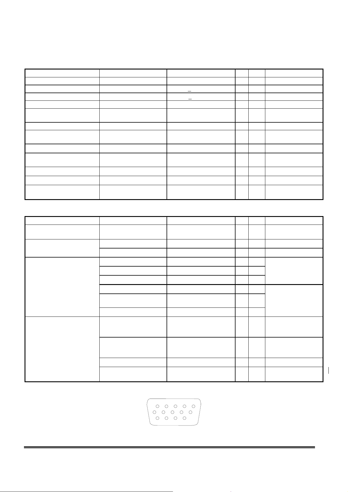
Note-1: The pin assignment of 15 pin D-sub connector:
Universal input full range 90~264VAC /47~63Hz
90 ~ 264VAC < 2.0 Arms
Normal “On” operation < 50 Watts
DPMS “Off” state < 3 Watts
110 VAC
220 VAC
264 VAC/50Hz < 3.5 mA
1. 1500VAC, 1 sec
2. Ground test: 30A, 1sec
IEC1000-4-4 1KV
IEC1000-4-5 (Surge) Common: 2KV,
90 ~ 264VAC 6mA ~ 15mA
90 ~ 264VAC 40KHz ~ 80KHz
Color: White or Black
15 pin D-Sub
15 pin D-sub connector See Note-1
24 pin DVI connector See Note-2
Signal type-1
Level
(R,G,B signals)
Impedance
Single-ended input swing
voltage (V-swing)
Impedance
Sync Pulse Width (SPW)
(R,G,B signals)
Signal type-2 TMDS signals
(TMDS signals)
Signal type Separate H/V-sync
Level Logic High: 2.4V ~ 5.5V
Impedance
Engineering Specification
< 30 A (peak)
< 60 A (peak)
Without damage
< 0.1 ohm
Differential: 1KV
Length: 1800 +/-
Color: White or Black
Length: 1600
Separate analog R,G,B signals
700 mV (peak to peak)
75 Ohms +/- 1.5 Ohms
200mV≤V-swing≤780mV
100 Ohms +/- 10 Ohms
Composite H/V-sync
(Positive/Negative)
Logic Low: 0V ~ 0.5V
Minimum 2.2K
0.7μs < H-SPW
1H < V-SPW
5
10
15
+/-
(TTL level)
Ω(pull down)
1
6
11
20 mm
20 mm
√
√
LED: Green
√
LED: Amber
√
Cold-start
√
√
(on-line test)
√
(in-lab test)
√
√
Each connector
√
√
Depends on shipping
√
requirement (99 level)
Depends on shipping
√
√
√
√
√
√
√
√
√
√
√
√
√
requirement (99 level)
For 15 pin D-sub
For 24 pin DVI
For 15 pin D-sub
For 24 pin DVI
For 15 pin D-sub
Refer to VESA VSIS
Standard V1R1
10KΩ for application
3
Page 7
DV172 LCD Monitor Service Guide
Pin Signal Assignment Pin Signal Assignment
1 Red video 9 PC5V (+5 volt power)
2 Green video 10 Sync Ground
3 Blue video 11 Ground
4 Ground 12 SDA
5 Ground 13 H-Sync (or H+V)
6 Red Ground 14 V-sync
7 Green Ground 15 SCL
8 Blue Ground
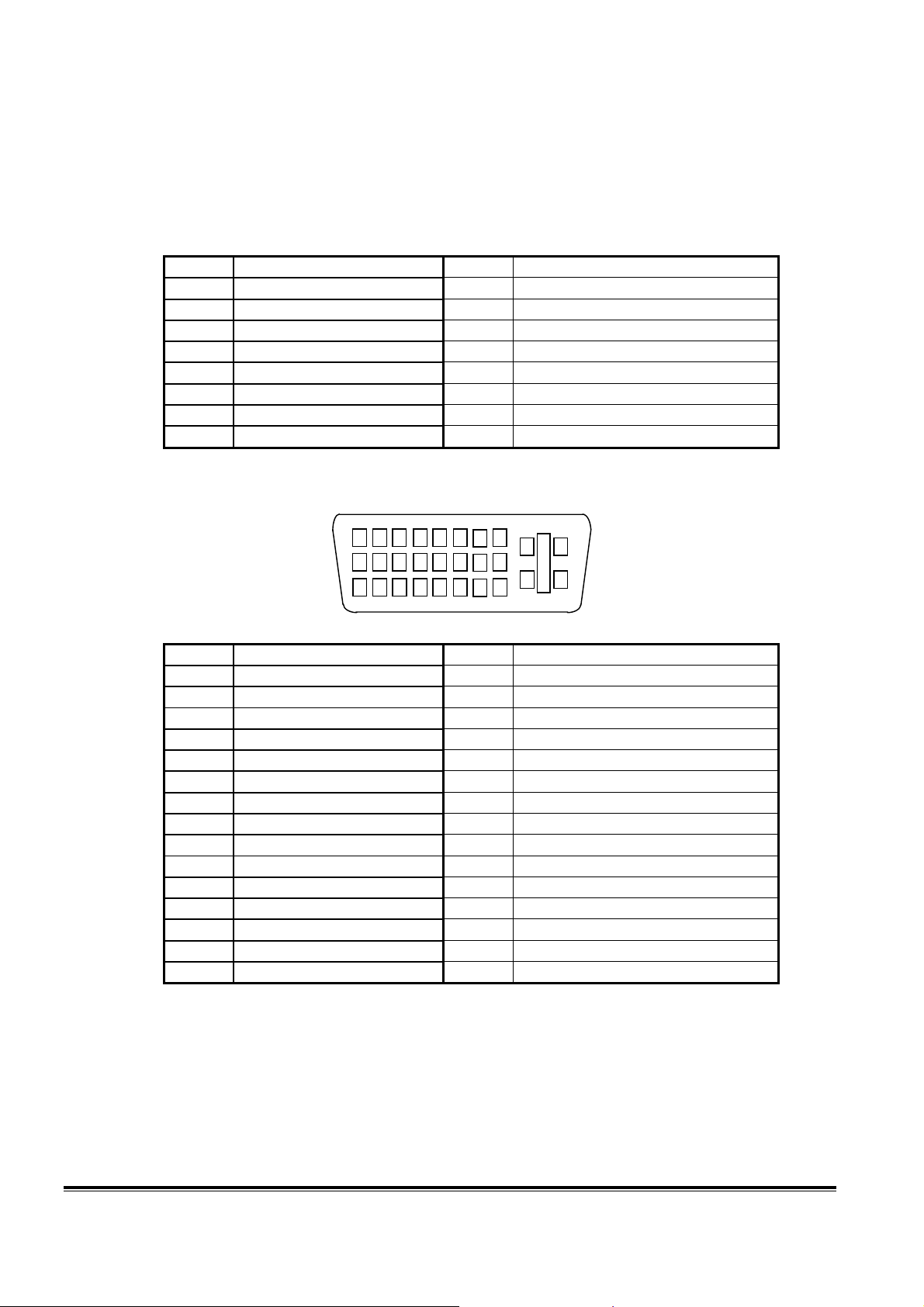
Note-2: The pin assignment of 24 pins DVI connector: (C1 ~ C5 are NC)
2345
1
9
10 11
171819
Engineering Specification
8
7
6
12
13
14
21
20
22
C1 C2
16
15
23
C5
C3
24
C4
Pin Signal Assignment Pin Signal Assignment
1 TMDS RX2- 16 Hot Plug Detect
2 TMDS RX2+ 17 TMDS RX03 TMDS Ground 18 TMDS RX0+
4 Floating 19 TMDS Ground
5 Floating 20 Floating
6 DDC Clock 21 Floating
7 DDC Data 22 TMDS Ground
8 Floating 23 TMDS Clock+
9 TMDS RX1- 24 TMDS Clock10 TMDS RX1+ C1 Floating (NC)
11 TMDS Ground C2 Floating (NC)
12 Floating C3 Floating (NC)
13 Floating C4 Floating (NC)
14 +5V Power C5 Floating (NC)
15 Ground
4
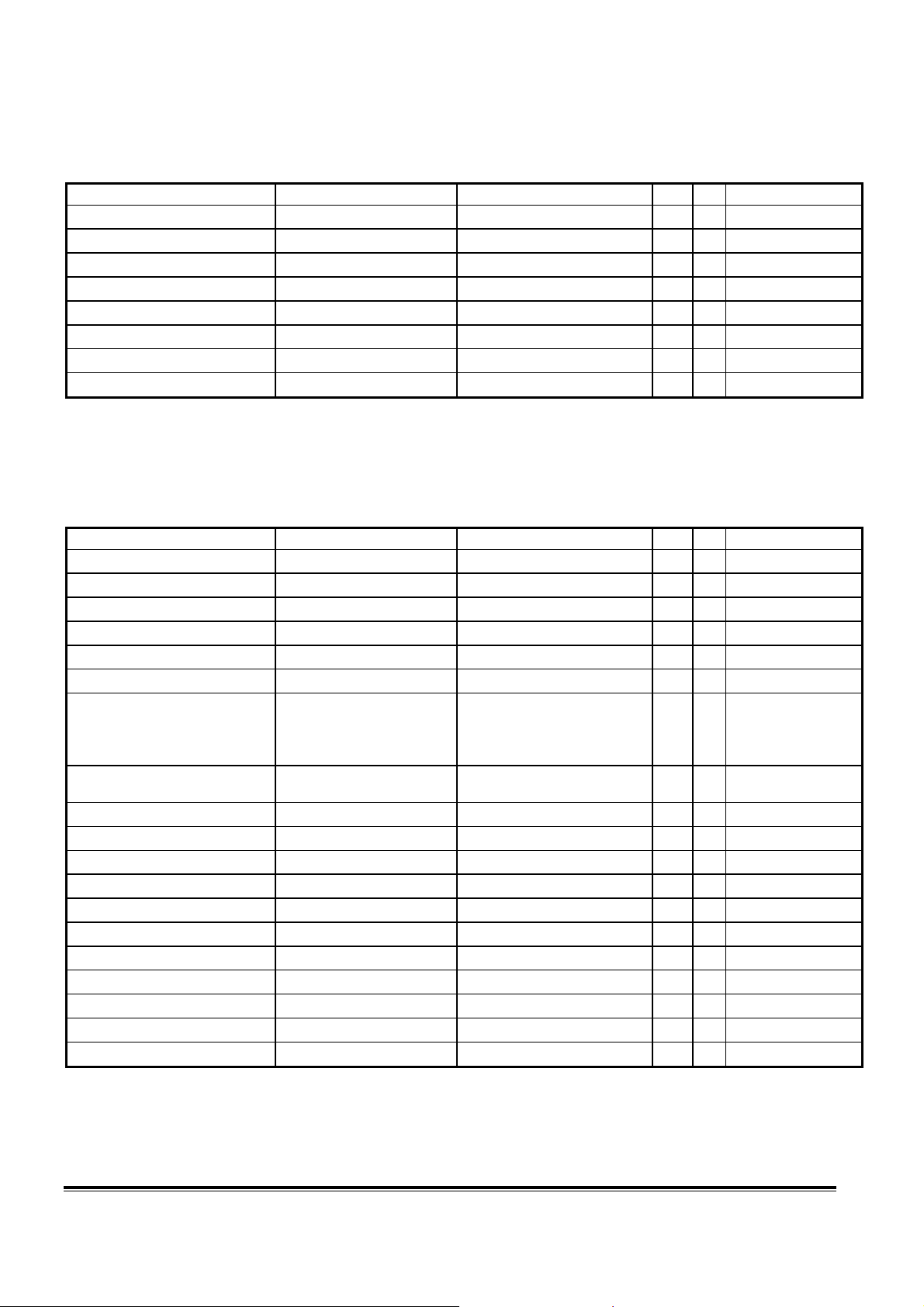
Page 8
DV172 LCD Monitor Service Guide
Engineering Specification
2.3 Video performance
Item Condition Spec OK N.A Remark
Max. support Pixel rate
Max. Resolution
Rise time + Fall time
Settling Time after
overshoot /undershoot
Overshoot/Undershoot
2.4 Scan range
Item Condition Spec OK N.A Remark
Horizontal
Vertical
2.5 Plug & Play DDC2B Support
Item Condition Spec OK N.A Remark
DDC channel type DDC2B
EDID Version 1.3
2.6 Support Timings
Input Timing
Resolution
640x350 31.47(P) 70.08(N) 25.17 1280x943
720x400 31.47(N) 70.08(P) 28.32 1280x1024
640x480 31.47(N) 60.00(N) 25.18 1280x1024
640x480 35.00(N) 67.00(N) 30.24 1280x1024
640x480 37.86(N) 72.80(N) 31.5 1280x1024
640x480 37.50(N) 75.00(N) 31.5 1280x1024
800x600 37.88(P) 60.32(P) 40.00 1280x1024
800x600 48.08(P) 72.19(P) 50.00 1280x1024
800x600 46.86(P) 75.00(P) 49.50 1280x1024
832X624 49.72(N) 74.55(N) 57.29 1280x1024
1024x768 48.36(N) 60.00(N) 65.00 1280x1024
1024x768 56.48(N) 70.10(N) 75.00 1280x1024
1024x768 60.02(P) 75.00(P) 78.75 1280x1024
Horizontal
Frequency (KHz)
135 MHz
1280 x 1024
< 3.7 ns
(50% of minimum pixel
clock period)
< 5% final full-scale value
< 12% of step function
voltage level over the full
voltage range
31 ~ 81KHz
56 ~ 75 Hz
Actual Output
Vertical
Frequency (Hz)
Dot Clock
Frequency (MHz)
Actual display
Resolution
√
√
1280x1024 @ 75Hz
√
√
√
√
√
√
√
(max. support timing)
Refer to VESA VSIS
Standard V1R1
Refer to VESA VSIS
Standard V1R1
Without Frame buffer
Refer to FP767-MEA
DV172 C212 S/W spec
document to see the
detailed EDID data
definition..
Remark
DOS
DOS
DOS
Macintosh
VESA
VESA
VESA
VESA
VESA
Macintosh
VESA
VESA
VESA
OK N.A
√
√
√
√
√
√
√
√
√
√
√
√
√
5
Page 9
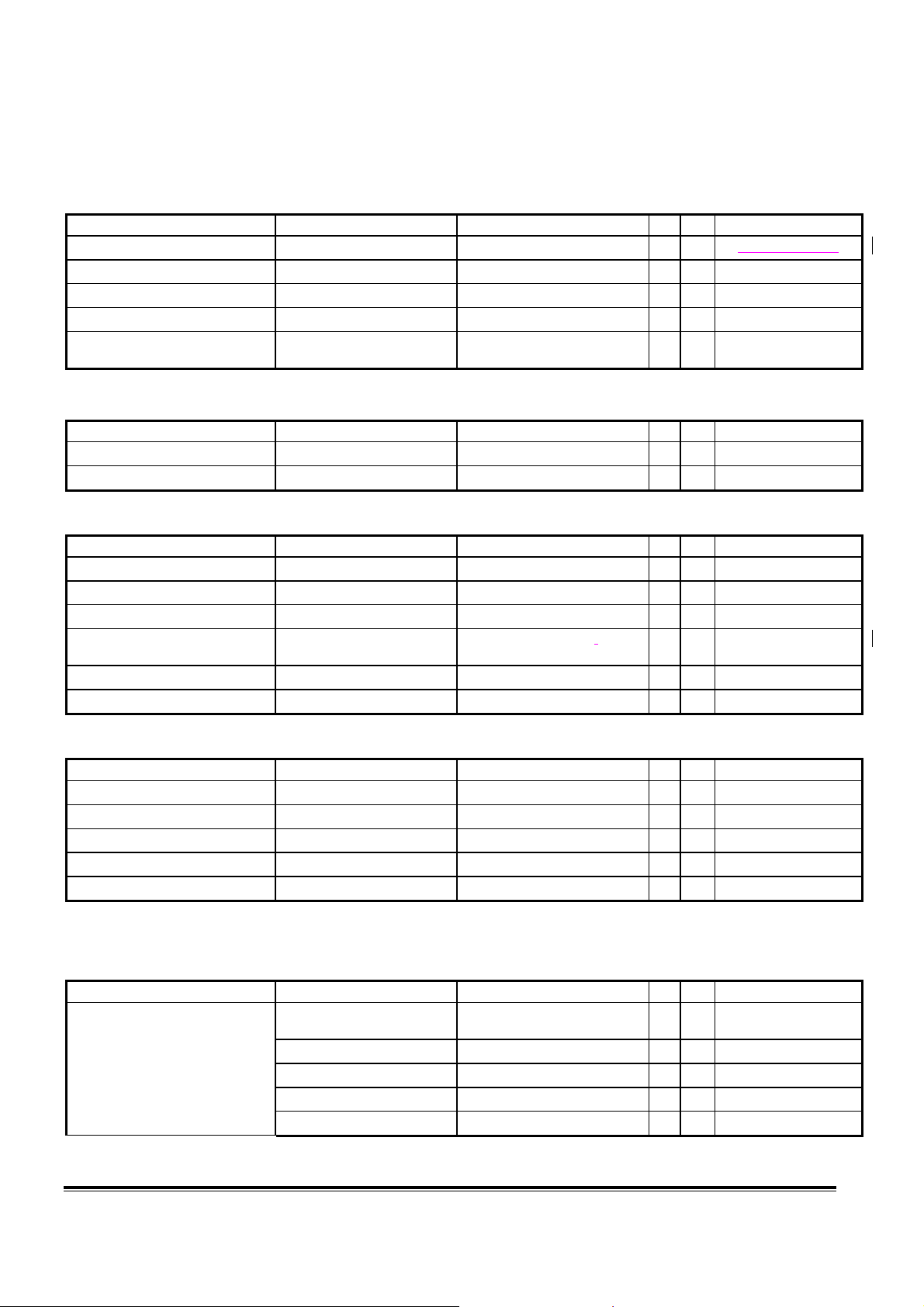
DV172 LCD Monitor Service Guide
Engineering Specification
Input Timing
Resolution
1024X768 60.24(N) 74.93(N) 80.00 1280x1024
1152x864 67.50(P) 75.00(P) 108.00 1280x1024
1152x870 68.68(N) 75.06(N) 100.00 1280x1024
1152x900 61.80(N) 66.00(N) 94.50 1280x1024
1152x900 71.81(N) 76.14(N) 108.00 1280x1024
1280x1024 64.00(P) 60.00(P) 108.00 1280x1024
1280x1024 75.83(N) 71.53(N) 128.00 1280x1024
1280x1024 80.00(P) 75.00(P) 135.00 1280x1024
1280x1024 81.18(N) 76.16(N) 135.09 1280x1024
Horizontal
Frequency (KHz)
Vertical
Frequency (Hz)
Dot Clock
Frequency (MHz)
Note-2: “P”, “N” stands for “Positive”, “Negative” polarity of incoming H-sync/V-sync (input timing)
Actual Output
Actual display
Resolution
OK N.A
√
√
√
√
√
√
√
√
√
Remark
Macintosh
VESA
Macintosh
SUN 66
SUN
VESA
IBM1
VESA
SPARC2
3. Operational & Functional Specification
3.1 Video performance
Item Condition Spec OK N.A Remark
Resolution
Contrast ratio
Brightness
Response time
Viewing angle
CIE coordinate of White
Display colors
3.2 Brightness Adjustable Range
Item Condition Spec OK N.A Remark
Brightness adjustable range
3.3 Acoustical Noise
Item Condition Spec OK N.A Remark
Acoustical Noise
Any input resolution modes
which are under 1280x1024
At R,G,B saturated condition
(Default “User” color setting)
Rising + Falling time 16 ms(typ.), 25ms(max.)
At Contrast ratio ≧ 10
At Contrast ratio ≧ 10
At Max. Contrast level &
Full-white color pattern
At 1 meter distance
& “Audio” function disabled
(0.31, 0.33) +/- (0.03, 0.03)
262144 color with dithering
1280 x1024
250:1(min.), 500:1 (typ.)
200 cd/m2(min.)
260 cd/m2(typ.)
R/L: 60 degrees (min.)
70 degrees (typ.)
U/D: 60 degrees (min.)
70 degrees (typ.)
(
Max. brightness value –
Min. brightness value)
≧ 40 cd/㎡
≦ 40 dB/A
√
√
√
√
√
√
√
18 bits with
√
√
√
dithering
6
Page 10
DV172 LCD Monitor Service Guide
3.4 Audio performance
Item Condition Spec OK N.A Remark
Preamp + Power amp
(1)Output power
(2)THD (@ 1W)
(3)S/N ratio
Speaker Driver
(1)Nominal impedance
(2)Maximum input power
(3)Frequency response
(4)Mean sound pressure level
(5)Size
Audio Control
(1)Volume range
(2)Mute
Engineering Specification
1 Wrms/CH @ 1KHz
<10%
40dB
8 ohm
2W/CH
12KHz
83 ± 3 dB
28x 40 mm
0 ~100 levels
On/Off
√
√
√
√
√
√
√
√
√
√
Real output
4. LCD Characteristics
4.1 The Physical definition & Technology summary of LCD panel
Item Condition Spec OK N.A Remark
LCD Supplier
Panel type of Supplier
Screen Diagonal
Display area
Physical Size
Weight
Technology
Pixel pitch
Pixel arrangement
Display mode
Support color
Unit=mm 337.920(H) x 270.336(V)
Unit=mm 358.5(W) x 296.5(H) x 19.0(V)
Unit=gram 1900 (typ.)
TN with Film
Unit=mm 0.264 x 0.264
AUO
M170EN05
432mm(17.0”)
R,G,B vertical stripe
Normally white
262K colors(R,G, B 6-bit data)
√
√
√
√
√
√
√
√
√
√
√
Per one triad
7
Page 11
DV172 LCD Monitor Service Guide
Engineering Specification
5. User Controls
5.1 User’s hardware control definition:
Item Condition Spec OK N.A Remark
Monitor Power button
Enter button
▲/Inc. button
▼/Dec. button
Exit button
Auto button
Mute button
Input source select button
5.2 OSD control function definition
Item Condition Spec OK N.A Remark
Contrast
Brightness
Horizontal Position
Vertical Position
Pixel Clock
Phase
Color Temperature
User
OSD Position
Language
OSD Time
Vo l u m e
Hot key for Contrast
Hot key for Brightness
Hot key for Volume
Auto adjustment
Information
Mute
Input Source select
Recall
OSD Horizontal position
C1: 9300
C2: 6500
C3: 5800
: Separate R,G,B adjustment
OSD Vertical position
6 languages
From 5 sec to 60 sec
Auto-Geometry/Color
For input timing
√
√
√
√
√
√
√
√
See Table 3
√
√
√
√
√
√
√
√
√
√
√
√
√
√
√
√
√
√
√
* The detailed Firmware functions’ specification, please refer to C212, S/W spec document.
8
Page 12
DV172 LCD Monitor Service Guide
Engineering Specification
6. Mechanical Characteristics
6.1 Dimension
Item Condition Spec OK N.A Remark
Bezel opening
Monitor without Stand
Monitor with Stand
Carton Box (outside)
Tilt and Swivel range
L x W x H mm 382.7x118x402.85 mm
L x W x H mm 382.7x200x404.3 mm
L x W x H mm 495x450x158 mm
Tilt : 0/20 degree
6.2 Weight
Item Condition Spec OK N.A Remark
Monitor (Net)
Monitor with packing
(Gross)
6.3 Plastic
Item Condition Spec OK N.A Remark
Flammability
Heat deflection To
UV stability
Resin
Texture
Color
6.4 Carton
Item Condition Spec OK N.A Remark
Color
Material
Compression strength
Burst Strength
Stacked quantity
340x272.4 mm
Swivel:0 degrees
4.7Kg
6.5Kg
94HB
ABS
ABS Delta E < 8.0
MPR2 : ABS
(VW55/VE0856/D350)
MT-11030
Pearl White
65 ℃
Kraft
B Flute
530 KGF
16 KGF/cm2
13 Layers
Refer to Table 6
√
√
√
√
√
√
√
√
√
MPR2/TCO
√
√
√
√
√
√
√
√
√
7. Certification
Item Condition Spec OK N.A Remark
Environment Green design API Doc. 715-C49
Blue Angel German Standard
E-2000 Switzerland
EPA USA Standard
EN61000-3-2 Harmonics
9
√
√
ISO14000
Requirement
√
√
√
Page 13
DV172 LCD Monitor Service Guide
Engineering Specification
TCO92/95
TCO99
PC-Monitor Microsoft Windows PC98/99
DPMS VESA
DDC 2B Version 1.3
USB External
Safety UL (USA) UL 1950 3rd edition
CSA (Canada) C22.2 No. 950-M95
FIMKO EN60950
IEC950
EN60950
73/23/EEC
CB
TUV/GS EN60950
CCIB (China)
EIAJ/JEIDA (Japan)
Item Condition Spec OK N.A Remark
NOM (Mexico)
JEON (Korea)
EZU
PSB
EMC CE Mark 89/336/EEC
FCC (USA) Class B
EN55022 Class B
CISPR 22 Class B
VCCI (Japan) Class B
BSMI (Taiwan)
C-Tick (Australia) AS3548
RRL (Korean)
X- Ray Requirement DHHS (21 CFR) USA X- Ray Standard
DNHW
PTB German X- Ray standard
MPRII
MPRIII
Ergonomics ZH1/618 German ergonomic
ISO 9241-3 -7 & 8
√
√
√
√
√
√
√
√
√
√
√
√
√
√
√
√
√
√
√
√
√
√
√
√
√
√
√
√
√
√
√
√
√
√
√
10
Page 14
DV172 LCD Monitor Service Guide
Engineering Specification
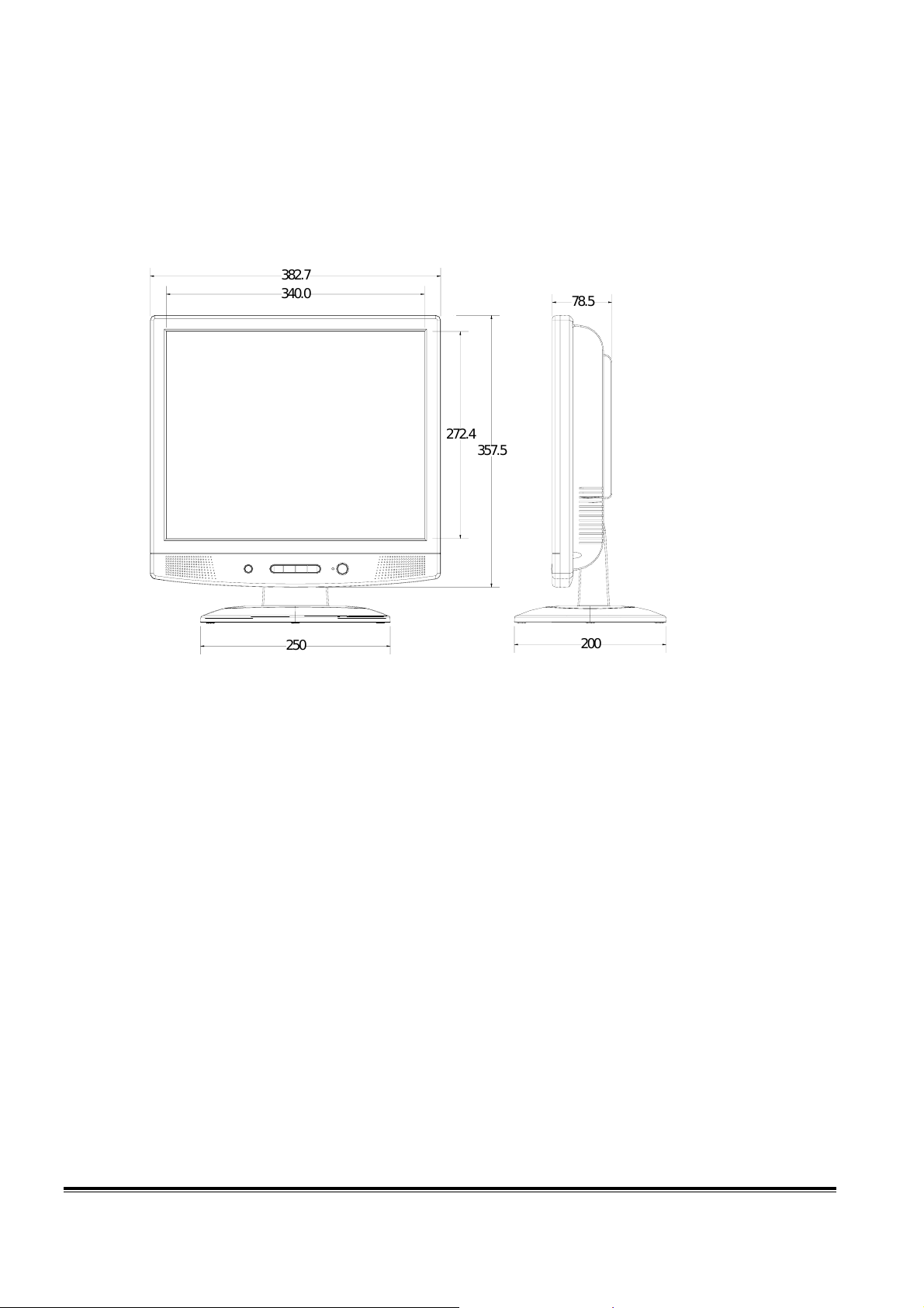
Appendix: Physical Dimension Front View and Side view
382.7
340.0
272.4
357.5
78.
5
250
200
11
Page 15

DV172 LCD Monitor Service Guide
Circuit Operation Theory
I. Introduction:
DV172 model is a 17” SXGA (1280x1024) 18 bits color TFT LCD monitor with multi-media function.
The features of DV172 are as below,
(a)Dual signal input supported for a 15pins D-sub and a DVI-D input connectors.
(b)It’s compliant with VESA DPMS spec to offer a smart power management and power saving function.
(c)OSD menu supported for users to control the adjustable items and get some information about this monitor.
(d)”Auto” button function supported to offer users an easy method to set all adjustable & controlled items well
by just pressing one button, “Auto”.
(e)VESA DDC2B function supported.
(f)Audio function supported with 2 speakers.
II. Block diagram
DV172 consists of a head and a stand (base). The head consists of a LCD module with 4 lamps, a power
board (include AC-DC, inverter power & audio circuit), a control board and an interface board. The block
diagram is shown as below.
To
backlight
Speaker
TFT-LCD module with 4 CCFL(backlight)
Interface board
Inverter
+
AC-DC board
+
Audio circuit
Audio
AC
socket
AC input
IN
Power sequence
circuit
Scaler Power
Control board
Analog RGB signals
Flash
ROM
EEPROM
DDC
IC
LVDS xtmr
Scaler
(Genesis
gm5120)
D-sub
connector
ADC
TMDS rcvr
DDC
IC
Speaker
DVI-D(TMDS) signals
DVI-D
connector
III. Circuit operation theory for electrical circuits in HEAD of DV172:
A.) Interface board diagram:
1
Page 16
DV172 LCD Monitor Service Guide
Circuit Operation Theory
Interface Board
RX0
RX1
RX2
RXC
Red
Green
Blue
Vsync
Hsync
(H+V)
SCL
SDA
DSCL
DSDA
A/D
TMDS
MCU
Scaling
OSD
Gm5120
FLASH-
ROM
DDC DDC
EEPROM
To
LCD
module
(a) Circuit operation theory: (The scaling IC used in DV172 is Genesis gm5120)
A basic operation theory for this interface board in Analog input signals processing, the scaling IC
inside A/D converter will convert analog input signals of Red, Green and Blue to 8 bits digital signals of
Red, Green and Blue, and for interface board in DVI-D(TMDS) digital input signals processing, the scaling
IC inside TMDS receiver will convert TMDS signals to 8 bits digital signals of Red, Green and Blue. Then
no matter input signals Analog or DVI-D(TMDS) format are, they have been converted to 8 bits digital Red,
Green and Blue signals, and the scaling IC inside MCU and scaling control circuit will start to do timing
signal detecting and calculating to output the proper LCD panel signals to LCD panel circuit.
The timing signal detecting function in the scaling IC is to detect whether input H-sync, V-sync or
digital pixel clock signals’ status have been changed by host PC system, then it will do short-time picture
blanking, signal processing and converting again if input signals have been changed.
The scaling IC inside OSD circuit will be programmed to an OSD menu which can be showed on the
screen to offer adjustable functions to end-users to control and adjust some picture settings by themselves.
After the scaling IC internal signal processing is done, it will output the digital RGB data, the H-sync,
V-sync, pixel clock and DE(data enable) signal to LVDS transmitter and then to LCD panel driver circuit.
There are two kinds of EEPROM used in interface board, one is 24C02 which is used to store DDC
2
Page 17

DV172 LCD Monitor Service Guide
data, we also call it, DDC IC, and another is to store OSD common data and those picture controlled and
data.
Flash-Rom is to store the source code which will be accessed by the scaling IC inside MCU to run
program.
(b) IC introduction:
1.) DDC (Display Data Channel) function: We use DDC IC to support DDC/2B function. DDC data is
stored in 24C02(EEPROM). Those data related to LCD monitor specification. PC can read them by
“SDA” and “SCL”(“DSDA” & “DSCL” for DVI-D input port) serial communication for I2C
communication for DDC2B.
2.) Gm5120 IC: There are A/DC, TMDS receiver, Scaling, OSD, MCU in the gm5120 IC. Scaling IC is
revolutionary scaling engine, capable of expanding any source resolution to a highly uniform and sharp
image or down scaling from UXGA, combined with the critically proven integrated 8 bit triple-ADC
and patented Rapid-lock digital clock recovery system. It also support detect mode and DPMS control.
Circuit Operation Theory
MCU control unit, it controls all the functions of this interface board, just like the OSD display setting,
the adjustable items, adjusted data storage, the external IIC communication, support DDC2B.
3.) EEPROM: All the adjustable data and user settings are stored in EEPROM (24C16).
4.) FLASH ROM: To store source code which will be accessed by Scaling IC inside MCU to run program.
B.) Power board diagram:
EMI Filter Rectifier and
filter
Isolation power
transformer
Rectifier and filter Audio Amp and
Pre-Amp
Inverter circuit
PWM controller Switching element
Feedback Isolation
3
Rectifier and filter
LDO regulator
Page 18

DV172 LCD Monitor Service Guide
(a) EMI Filter
This circuit (fig. 2) is designed to inhibit electrical and magnetic interference for meeting FCC, VDE,
VCCI standard requirements.
Circuit Operation Theory
Fig. 2
(b) Rectifier and filter
AC Voltage (90-264V) is rectified and filtered by BD601, C605 (See Fig 3) and the DC Output
voltage is 1.4*(AC input). (See Fig.3)
Fig. 3
(c) Switching element and Isolation power transformer
When the Q601 turns on, energy is stored in the transformer. During Q601 turn-off period, the stored
energy is delivered to the secondary of transformer. R607, C607 and D601 is a snubber circuit. R615 is
current sense resistor to control output power. (See Fig.4)
4
Page 19

DV172 LCD Monitor Service Guide
Circuit Operation Theory
Fig. 4
(d) Rectifier and filter
D701 and C703 are to produce DC output. L701 and C704 are to suppress high Frequency switching
spikes. (See Fig.5)
Fig. 5
(e) PWM Controller
The current mode control IC UC3842B is used to control PWM. When the VCC terminal of it gets
16V, IC601 turns on. +5V will be set up at Pin8 through soft start circuit, which includes R617, C611,
D606 and D605. R616 and C610 generate a fixed frequency saw-tooth wave at Pin4.
5
Page 20

DV172 LCD Monitor Service Guide
Circuit Operation Theory
Fig. 6
(f) Feedback circuit
PC123 is a photo-coupler and TL431 is a shunt regulation. They are used to detect the output voltage
change and be the primary and secondary isolation. When output voltage changes, the feedback voltage
will be compared and duty cycle will be decided to control the correct output voltage. (See Fig.7)
Fig. 7
6
Page 21

DV172 LCD Monitor Service Guide
(g) Audio circuit:
Connect with
PC Audio output
Circuit Operation Theory
Connect with
8 ohm/2W
Speaker
DC POWER
INPUT
POWER IC
TDA7496
AUDIO
INPUT
The Audio circuit is in Power board. The Audio Speaker has DC Volume control, use
28mmX40mm Speaker (2W per channel), power supply from AC-DC board and Audio input from
PC Audio output (Line Out).
1.)Power IC: Use ST POWER IC TDA7496.The IC are stereo Class AB output amplifiers with DC
Volume control. The devices are designed for use in TV and monitor, but are also suitable
for battery-Fed portable recorders and radios. Use +15V from AC-DC Board and connect
speaker to offer 1W per channel.
2.)DC Power Input: To supply +15V to be VCC source Voltage for TDA7496 and built-in AC-DC board.
3.)Audio Input: connect with PC Audio output in 3.5mm to 3.5mm signal line.
4.)Speaker: Use 8 ohm and 28mmX40mm speaker (2W/per channel)
5.)DC Volume Control: The voltage range is 1 – 5 V (From MC)
7
Page 22

DV172 LCD Monitor Service Guide
Circuit Operation Theory
8
Page 23

DV172 LCD Monitor Service Guide
Circuit Operation Theory
(h) Inverter circuit:
1.) Block Diagram:
15Vin
ON/OFF
BRT_ADJ
2.) General Specification
Input Voltage: 15V
Input Current: 2A max.
ON/OFF Voltage: 3.3V
PWM Duty: 3.3V/47KHz
ON/OFF
switching
PWM CONTROLLER
TL1451 CIRCUIT
OSCILATOR
CIRCUIT
TRANSFORMER CCFL
PROTECTION
AND DETECT
Output Requirement:
Max. Output Current: 15mA
Min. Output Current: 6mA
Lamp Working Voltage: 600Vrms
Open Lamp Voltage: 1800Vrms
Frequency: 55KHz
9
Page 24

DV172 LCD Monitor Service Guide
3.)Circuit Operation Theorem
3.1) ON/OFF SWITCH
Circuit Operation Theory
The turn-on voltage was controlled by R756 and R757.The inverter was turned on or off by the
switching transistors Q761 and Q757, Also regulator IC751 is control by Q761 and Q757 decide
supply 15V to inverter part or instead.
10
Page 25

DV172 LCD Monitor Service Guide
3.2) PWM Control circuit
Circuit Operation Theory
TL1451 is a dual PWM controller.C765 and R765 decide the working frequency.BLT_ADJ
signal is from control board, control pulse width then decide how much energy delivery to CCFL also
decide CCFL brightness. Q741 and Q742 be the buffer to rise the drive capability and the totem poles
circuit can improve a capable of driving for Q743.C770 decide the striking time delay.
11
Page 26

DV172 LCD Monitor Service Guide
3.3) Oscillator Circuit
Circuit Operation Theory
Royer circuit uses the characteristic of transformer saturation to oscillate. When the DC power inject,
Q759 or Q760 will turns on, and the current Ic increases. After a period, the transistor will leave the
saturation status and Vce increase. The result causes the voltage of primary coil get lower. Finally the
transistor turn off, and another transistor turn on. These statuses are repeated and the pin7 and pin8 of
T751 will get a Sin Wave to turn on CCFL.
C.) Control board introduction:
The main parts of the control board are a push button, and a led.
(a) Push button:
It’s a simple switch function, pressing it for “ON” to do the auto adjustment
function, releasing it for “OFF” to do nothing.
(b) Led:
It indicates the DPMS status of this LCD monitor; green light means DPMS on (Normal
operating condition). Amber light means DPMS off (Power off condition).
12
Page 27

DV172 LCD Monitor Service Guide
Table of Contents
1. Alignment procedure (for function adjustment)..............................................................................2
A. Preparation: ......................................................................................................................2
B. Timing adjustment: (Analog only, it’s no need for DVI-D input source)........................2
C. Auto color balance adjustment: (Analog only, it’s no need for DVI-D input source) .....2
D. Color adjustment: (Analog only)......................................................................................2
E. Writing EDID file: (Analog and DVI-D both) .................................................................3
F. Command definition for Auto Alignment:........................................................................3
2. Wire Dressing..................................................................................................................................4
3. Add Glue.........................................................................................................................................7
4.Touch Up..........................................................................................................................................8
Alignment procedure
1
Page 28

DV172 LCD Monitor Service Guide
Alignment procedure
1. Alignment procedure (for function adjustment)
The list of necessary alignment for a LCD monitor:
Items Description Remark
1 Timing adjustment Preset timing
2 Auto color balance adjustment SVGA2 60Hz
3 Color temperature adjustment C1, C2 & C3
4 Writing EDID file Analog and Digital
A. Preparation:
1. Setup input timing to any preset modes, any patterns.
2. Enter factory mode (press “EXIT” & “ENTER” at the same time, then press “power” button to turn on monitor).
3. Move blue cursor into “BURN IN MODE” tag and select “YES” to enable burn-in mode.
4. Power off the monitor, then power on again.
5. Setup unit and keep it warm up at least 30 minutes.
B. Timing adjustment: (Analog only, it’s no need for DVI-D input source)
1. Enter factory mode (press “EXIT” & “Enter” at the same time, then press “power” button to turn on monitor).
2. Select timing from figure-1. The timing marked with star sign (*) have to be adjusted with Analog signals from
Chroma video pattern generator..
3. Press AUTO key to run “AUTO adjustment” function.
4. Clear user area in EEPROM.
5. Check the phase of the image; if phase is not perfect adjust it to the best condition.
6. Adjust the settings to following values:
CONTRAST = 55
BRIGHTNESS = 90
OSD TIME = 20
VOLUME = 20
COLOR = USER
7. Press “EXIT” key until the “SAVE” show s on the OSD to save factory parameters and turn off the monitor power.
8. Turn on the power enter user mode.
C. Auto color balance adjustment: (Analog only, it’s no need for DVI-D input source)
1. Setup input timing SVGA2 (800x600@60Hz), pattern 1(crosshatch pattern with white color frame) with Analog
signals from Chroma video pattern generator.
2. Enter factory mode (press “EXIT” & “Enter” at the same time, then press “power” button to turn on monitor).
3. Move blue cursor into “BURN IN MODE” tag and select “YES” to enable burn-in mode.
4. Set color pointer to USER mode
5. Press “ ▼ ” button to do white balance for auto color balance adjustment.
D. Color adjustment: (Analog only)
1. Setup input timing to any preset modes, pattern 41(full white color pattern) with Analog signals from Chroma video
pattern generator.
2
Page 29

DV172 LCD Monitor Service Guide
Alignment procedure
2. Enter factory mode (press “EXIT” & “ENTER” at the same time, then press “power” button to turn on monitor).
3. Confirm auto color balance adjustment had already been done.
4. Measure each color temperature (C1, C2 & C3) by Minolta CA-110 (or equivalent equipment).
5. Two methods can be used to adjust RED, GREEN, BLUE value of each color temperature, C1, C2 & C3 to meet
following spec requirement, the 1
adjustment, and the 2
nd
method is by manually and must be in factory mode.
Color temperature
(C1, 9300K set on OSD)
st
method is by using external PC and IIC alignment protocol to do automatic
X+- 0.283+(-) 0.03
Y+- 0.297+(-) 0.03
X+- 0.313+(-) 0.03 Color temperature
(C2, 6500K set on OSD)
Y+- 0.329+(-) 0.03
X+- 0.326+(-) 0.03 Color temperature
(C3, 5800K set on OSD)
Y+- 0.342+(-) 0.03
6. Turns off the monitor power.
E. Writing EDID file: (Analog and DVI-D both)
1. Setup a PC with DDC card.
2. Connect PC to monitor with a D-sub signal cable.
3. Please refer to the C212 for the correct EDID file.
4. Runs the writing program to write the EDID file into EEPROM for analog input.
5. Read both EEPROM data and confirm if it’s matched with the C212 definition.
Repeat the above step 1 to step 5 with DVI-D signal cable connected.
6.
F. Command definition for Auto Alignment:
1. PC Host will send 0x7C IIC slave address and then following 4 bytes command
I2C Send Command Byte1 Byte2 Byte3 Byte4
Change Color Temperature to C1 CC 1 XX checksum
Change Color Temperature to C2 CC 2 XX checksum
Change Color Temperature to C3 CC 3 XX checksum
Change C/T to User CC 4 XX checksum
User mode to factory mode 1A 5A XX checksum
Auto Color (Offset1, Offset2, Gain) 1B 5A XX checksum
Factory mode to User mode 1E 5A XX checksum
Clear user area data 1F 5A XX checksum
Off burn in mode CE 2 XX checksum
Change language setting 66 0~5 XX checksum
Note A: Byte4(Checksum) = Byte1 + Byte2 + Byte3
Note B: Data = The value write to MCU
Note C: XX = don't care, any value(<=0xFF).
Note D: The Byte-2 definition of “Change Language Setting” is as below,
0=DE, 1=EN, 2=ES, 3=FR, 4=IT, 5=JA
2. When PC Host sends 0x7D command to MCU, MCU must return as following (2 bytes)
Return Code R-Byte1 R-Byte2
Checksum error code FC AA
Normal return code the above Byte3 (/data) FC
If normal return code is exact FCh FC CF
3
Page 30

DV172 LCD Monitor Service Guide
Alignment procedure
3. The Table is for alignment machine to read data from EEPROM to check if the alignment process and write data are
correct.
I2C Send Command Byte1 Byte2 Byte3 Byte4
Read EEPROM Contrast A3 92 XX checksum
Read EEPROM Brightness A3 93 XX checksum
Read EEPROM C/T Point A3 94 XX checksum
Read EEPROM OSD-Hpos A3 95 XX checksum
Read EEPROM OSD-Vpos A3 96 XX checksum
Read EEPROM Language A3 97 XX checksum
Read EEPROM OSD Timer A3 98 XX checksum
Read EEPROM Volume A3 99 XX Checksum
Figure-1: Preset Timing modes list
Resolution
640x350 31.47(P) 70.08(N) 25.17 DOS 1280x943
720x400 31.47(N) 70.08(P) 28.32 DOS
640x480 31.47(N) 60.00(N) 25.18 DOS
640x480 35.00(N) 67.00(N) 30.24 Macintosh
640x480 37.86(N) 72.80(N) 31.5 VESA
640x480 37.50(N) 75.00(N) 31.5 VESA
800x600 37.88(P) 60.32(P) 40.00 VESA
800x600 48.08(P) 72.19(P) 50.00 VESA
800x600 46.86(P) 75.00(P) 49.50 VESA
832X624 49.72(N) 74.55(N) 57.29 Macintosh
1024x768 48.36(N) 60.00(N) 65.00 VESA
1024x768 56.48(N) 70.10(N) 75.00 VESA
1024x768 60.02(P) 75.00(P) 78.75 VESA
1024X768 60.24(N) 74.93(N) 80.00 Macintosh
1152x864 67.50(P) 75.00(P) 108.00 VESA
1152x870 68.68(N) 75.06(N) 100.00 Macintosh
1152x900 61.80(N) 66.00(N) 94.50 SUN 66
1152x900 71.81(N) 76.14(N) 108.00 SUN
1280x1024 64.00(P) 60.00(P) 108.00 VESA
1280x1024 75.83(N) 71.53(N) 128.00 IBM1
1280x1024 80.00(P) 75.00(P) 135.00 VESA
1280x1024 81.18(N) 76.16(N) 135.09 SPARC2
Horizontal
Frequency (KHz)
Vertical
Frequency (Hz)
Dot Clock
Frequency (MHz)
Remark
Actual display
resolution
Full screen
1280x1024
2. Wire Dressing
A point for attention is marked in yellow circle and wire allocation are shown as below:
a.) Internal structure of LCD monitor
4
Page 31

DV172 LCD Monitor Service Guide
b.) Speaker wire
Alignment procedure
5
Page 32

DV172 LCD Monitor Service Guide
c.) LVDS wire
d.) Power grounding
Alignment procedure
6
Page 33

DV172 LCD Monitor Service Guide
e.) Control wire
3. Add Glue
Alignment procedure
The below attached figure shows the location of added glue component.
a.)The location of add glue component have L602, L603, C605, C603, C604, C615, C703, C704, and C707.
b.) CN601, C605, Q601, T601, D701, D7021 and IC701.
7
Page 34

DV172 LCD Monitor Service Guide
Alignment procedure
4.Touch Up
Remark: The manufacturing site should base on their experience and pass the necessary testing to add or reduce
some touchup points.
8
Page 35

DV172 LCD Monitor Service Guide
1. No Display or display is unstable:
1.1 Interface Board:
Y
N
Y N
No picture or picture
unstable
Power off?
Does Cable plug in
connector?
Is power stable?
N
Turn On Power
Plug all wire then turn on
power again
Check J5 connector or
power BD
Trouble Shooting
Cables used in DV172:
(1) Internal:
(a)LVDS wire to panel:J6 & J7
(b)Wire to control BD: J4
(2) External:
Signal cable: J1 and J2
Y
N
Is LED light green?
Y N
Does 7414 (U2) work
well?
Y
Is DVI signal well?
Y
N
N
Does crystal work
correctly?
Check control BD
Check 7414 related circuit or replace it
Check (U3) DDC data of digital
input
Check crystal (Y1) CKT or replace it
Y
Check Panel or replace it
2. BUTTON function:
1
Page 36

DV172 LCD Monitor Service Guide
2.1 Control Board
OSD is not working
Yes
Is control BD connecting? No Plug control BD then retry
Yes
Is bottom switch normally? Yes Replace control BD then retry
No
Replace Control BD
Is OSD working??
Trouble Shooting
No
Check Interface BD
2
Page 37

DV172 LCD Monitor Service Guide
3. OSD function:
OSD doesn’t work
Is control BD working? No Replace control BD
Check interface BD
Trouble Shooting
3
Page 38

DV172 LCD Monitor Service Guide
4.Power Board
Backlight didn't shine
Trouble Shooting
Plug CN701 again or
checking I/F BD
Plug CN701 again or
checking I/F BD
Insert them ag ain
Y
IC751 PIN 9 IS 15V?Replace Q761
N
N
Turn on level existed?
N
Check CN752, CN 753
was pluged properly?
Replace IC751,Q751
N
PWM existed?
(BLT_ADJ)
Y
(BLT_ON)
Y
Y
Y
LED shined?
N
Y
3.3V existed? IS I/F board connected?
Y
Replace new fuse
N
Y
Check IC701 OK ?
N
Checking F601
Broke?
N
Check IC601 Vcc
existed?
Y
Y
Replace IC701
Replace new fuse
Replace
IC601,Q602,Q603
R602
N
Replace new fuse
N
Replace IC602,
IC702,D701 or check
I/F BD
4
Page 39

Model: DV172
No. PART NO. DESCRIPTION LOCATION
1 55.L5301.021 PCBA I/F BD MAXDATA
2 09.10612.01B CAPACITOR EL 10U 25V M RF2.5 C69 C72 C79 C85
3 09.22612.01B CAP EL 22U 25V M RF2.5 C14 C17 C23 C28 C33 C40 C41
3 09.22612.01B CAP EL 22U 25V M RF2.5 C88 C90 C97 C99
4 09.47612.01V CAP EL 47U 25V M RT2.5 C83
5 20.22003.024 CONN RECE DVI-A 24+6P RT MOLE J2
6 20.24012.A15 CONN D FML 3R15P RT BLU S WO/ J1
7 20.60089.108 HEAD BLK 1R 8P D2 3S H6 J7
8 20.60091.109 HEAD BLK 1R9P RT D2 3S H4.8 J4
9 20.72060.207 HEAD FML 2R14P D2.54 H8.4 J5
10 45.10101.071 LABEL(B)SERIAL ART 12*5 ALL
11 47.L5305.001 GASKET 6X10X2T
12 55.L5301.M21 PCBA I/F BD MAXDATA M/I
13 71.05120.00E IC LCD CTRL GM5120 PQFP 208P U4
14 71.06383.00I IC LVDS 24B THC63LVDM83A TSSO IC1 IC2
15 72.02402.C01 IC EEPROM AT24C02N-10SI-1.8SO U1 U3
16 72.02416.N01 IC EEPROM AT24C16N-10SI-1.8SO U7
17 73.07414.061 IC CMOS 74LVC14A SO-N 14P U2
18 74.01206.07C IC LDO IRU1206-25CY SOT-223 3 U5
19 74.06300.C3B IC RESET V6300C LO-2.8V SOT23 U9
20 72.39010.V33 IC FLASH SST39VF010-70 PLCC32 U6
21 55.L5302.021 PCBA SPS BD FR-1
22 04.01451.070 IC PWM CTRL TL1451ACN DIP 16P IC751
23 04.03842.044 IC VR UC3842BN DIP 8P IC601
24 04.07496.010 IC AMP TDA7496 SIP 15P IC501
25 05.00123.010 IC OPTO PC123F1 DIP 4P IC602
26 06.05707.010 XTOR SW 2SC5707 NPN TP 3P Q740 Q760 Q739 Q759
27 06.09024.020 FET MOS IRFU9024 PC TO-251AA Q743 Q751
28 06.2R060.151 DIODE BRI 2KBP06ML-530 600V 2 BD601
29 06.3R006.110 DIODE S.B. SB360 60V 3A DO-20 D751 D761
30 08.2703M.34D CAP DISC 27P3KV J SL 125 RF7. C736 C737 C756 C757
31 08.33216.354 CAP DISC Y1 3300P 250V RF10 D C603 C604
32 08.47216.354 CAP DISC Y1 4700P 250V RF10 D C615
33 09.1071M.L84 CAP EL 100U 450V M 105 25*25S C605
34 09.10813.L9C CAP EL 1000U35V RF5 L 13*25EL C703 C707 C704
35 09.1081D.09C CAP EL1000U16V RF5 105C 10*20 C508 C710
36 11.2241N.11E CAP X 0.22U U/V/FI 275V RF15 C602
37 13.10135.07E RES MOFM 100 2W J AF15 MINI R625
38 13.3R335.07E RES MOFM 3.3 J 2W AF15 MINI R513
39 13.68335.07E RES MOFM 68K J 2W AF15 MINI R607 R602
40 13.R2235.07E RES MOFM 0.22 J 2W AF15 MINI R615
41 17.60021.8R0 THERM 8 NTC 11.5D TR601
42 19.20267.001 XFORM PWR 450UH EI-30 T601
43 19.26038.001 XFORM INVERT 9.5UH EE19 T752 T754 T753 T751
44 19.40091.011 CHOKE 180UH T68-26 L602 L603
1
Page 40

45 19.40155.001 CHOK 2.7UH DR6*10 L701 L702
46 19.40179.001 CHOKE 71UH DR10*8 L752 L751
47 19.42008.011 LINE FILTER 30MH EE25 L601
48 20.60091.104 HEAD BLK 1R4P RT D2 3S H4.8 CN502
49 20.63174.104 HEAD ML 1R4P(-1#3) RT D4 4S H CN753 CN752
50 21.62052.207 HEAD ML 2R14P L RT D2.54 L10. CN701
51 22.10165.081 SKT EARJACK RT7P/PT284C BLU JK503
52 25.70029.001 BEAD 3T D6*10 Z580/100M L606 L607
53 26.12001.932 FUSE2A250V CERA ST20 T/LA RF2 F601
54 55.L5302.A21 PCBA SPS BD FR-1
55 60.L4606.001 ASSY HSK+UGF10DCT D701 D7021
56 60.L5308.011 ASSY AC SKT+WIRE+CORE E171FPB CN601
57 60.L5309.001 ASSY HSK+G960T IC701
58 55.L5303.031 PCBA CTRL BD FR-1
59 06.066GY.14X LED D5*8.3 GRN/YEL KTL-66GY-1 LD8601
60 22.40069.431 SW TACT 4.75MM RT TSVR-2
SW8601 SW8602 SW8603 SW8604 SW8605 SW8606
61 45.00091.021 LABEL ART 25*4.5 ALL
62 48.L5303.A00 PCB CTRL BD FR-1
63 50.L5301.011 WIRE 9/10P 1007#26 280MM NO-C CN8601
64 23.4L530.001 SPK*2 8 OHM 2W 470/150MM FP75
65 31.L5308.001 SPG-G SUS301 0.1T
66 33.L5306.001 BKT PNL SECC0.8T
67 34.L3703.001 SPG SUS301 0.1T
68 34.L5302.002 SHD SPTE0.4T
69 38.04121.001 TAPE 15*0.05MM KAPTON YEL
70 40.L3303.171 LBL SPEC LR DIAMOND
71 42.L5321.001 WIRE HLD ABS 002 I
72 42.L5325.001 WIRE-CLIP NYLON66 94V0 E171FP
73 42.L5326.001 MYLAR PET 35X20X0.4T E171FPB
74 47.L5306.001 AL TAPE 35X45 0.08T
75 47.L5307.001 AL TAPE 70X45 0.08T
76 50.L5302.001 WIRE 20+8/30P 1571 #28 120MM
77 56.91L53.001 LCDM 17" M170EN05/AUO
78 60.L5307.013 ASSY UC ABS 002 DVI
79 60.L5310.002 ASSY COLUMN ABSHB 002 B
80 60.L5316.001 ASSY BZL ABS HB 002 MEA
81 60.L5320.001 ASSY BASE W/PACK MEA
82 27.81318.011 CORD SAA #18*3C 10A 250V AUS
83 42.20019.002 BAG PE 250*350 LD
84 42.L0811.002 PE-HD BAG 600*650*0.05T 24LNG
85 44.L4001.131 CTN B DIAMOND(DV172)
86 45.00050.002 LABEL CTN ART 105*82 ALL(KB)
87 46.L0301.001 CARD WARR TFT LCD
88 47.L5301.002 CSN L EPS
89 47.L5302.002 CSN R EPS
90 49.L5303.001 INSTRUCTION MANUAL DV172
91 50.74405.201 CABLE AUDIO 284C/577C 002 140
92 50.L2308.201 SIGNAL/C 15/15P W/C 002/
93 50.L2508.201 SIGNAL/C DUAL DVI-D/DVI-D 200
2
Page 41

94 53.L5304.001 F DISK MEA DV172
3
Page 42

Model: DV172B (B = Black Cosmetic’s)
NO. PART NO. DESCRIPTION LOCATION
=== ============ ============================== =====================================
1 55.L5301.021 PCBA I/F BD MAXDATA
2 09.10612.01B CAPACITOR EL 10U 25V M RF2.5 C69 C72 C79 C85
3 09.22612.01B CAP EL 22U 25V M RF2.5 C14 C17 C23 C28 C33 C40 C41
3 09.22612.01B CAP EL 22U 25V M RF2.5 C88 C90 C97 C99
4 09.47612.01V CAP EL 47U 25V M RT2.5 C83
5 20.22003.024 CONN RECE DVI-A 24+6P RT MOLE J2
6 20.24012.A15 CONN D FML 3R15P RT BLU S WO/ J1
7 20.60089.108 HEAD BLK 1R 8P D2 3S H6 J7
8 20.60091.109 HEAD BLK 1R9P RT D2 3S H4.8 J4
9 20.72060.207 HEAD FML 2R14P D2.54 H8.4 J5
10 45.10101.071 LABEL(B)SERIAL ART 12*5 ALL
11 47.L5305.001 GASKET 6X10X2T
12 55.L5301.M21 PCBA I/F BD MAXDATA M/I
13 71.05120.00E IC LCD CTRL GM5120 PQFP 208P U4
14 71.06383.00I IC LVDS 24B THC63LVDM83A TSSO IC1 IC2
15 72.02402.C01 IC EEPROM AT24C02N-10SI-1.8SO U1 U3
16 72.02416.N01 IC EEPROM AT24C16N-10SI-1.8SO U7
17 73.07414.061 IC CMOS 74LVC14A SO-N 14P U2
18 74.01206.07C IC LDO IRU1206-25CY SOT-223 3 U5
19 74.06300.C3B IC RESET V6300C LO-2.8V SOT23 U9
20 72.39010.V33 IC FLASH SST39VF010-70 PLCC32 U6
21 55.L5302.021 PCBA SPS BD FR-1
22 04.01451.070 IC PWM CTRL TL1451ACN DIP 16P IC751
23 04.03842.044 IC VR UC3842BN DIP 8P IC601
24 04.07496.010 IC AMP TDA7496 SIP 15P IC501
25 05.00123.010 IC OPTO PC123F1 DIP 4P IC602
26 06.05707.010 XTOR SW 2SC5707 NPN TP 3P Q740 Q760 Q739 Q759
27 06.09024.020 FET MOS IRFU9024 PC TO-251AA Q743 Q751
28 06.2R060.151 DIODE BRI 2KBP06ML-530 600V 2 BD601
29 06.3R006.110 DIODE S.B. SB360 60V 3A DO-20 D751 D761
30 08.2703M.34D CAP DISC 27P3KV J SL 125 RF7. C736 C737 C756 C757
31 08.33216.354 CAP DISC Y1 3300P 250V RF10 D C603 C604
32 08.47216.354 CAP DISC Y1 4700P 250V RF10 D C615
33 09.1071M.L84 CAP EL 100U 450V M 105 25*25S C605
34 09.10813.L9C CAP EL 1000U35V RF5 L 13*25EL C703 C707 C704
35 09.1081D.09C CAP EL1000U16V RF5 105C 10*20 C508 C710
36 11.2241N.11E CAP X 0.22U U/V/FI 275V RF15 C602
37 13.10135.07E RES MOFM 100 2W J AF15 MINI R625
38 13.3R335.07E RES MOFM 3.3 J 2W AF15 MINI R513
39 13.68335.07E RES MOFM 68K J 2W AF15 MINI R607 R602
40 13.R2235.07E RES MOFM 0.22 J 2W AF15 MINI R615
41 17.60021.8R0 THERM 8 NTC 11.5D TR601
42 19.20267.001 XFORM PWR 450UH EI-30 T601
1
Page 43

43 19.26038.001 XFORM INVERT 9.5UH EE19 T752 T754 T753 T751
44 19.40091.011 CHOKE 180UH T68-26 L602 L603
45 19.40155.001 CHOK 2.7UH DR6*10 L701 L702
46 19.40179.001 CHOKE 71UH DR10*8 L752 L751
47 19.42008.011 LINE FILTER 30MH EE25 L601
48 20.60091.104 HEAD BLK 1R4P RT D2 3S H4.8 CN502
49 20.63174.104 HEAD ML 1R4P(-1#3) RT D4 4S H CN753 CN752
50 21.62052.207 HEAD ML 2R14P L RT D2.54 L10. CN701
51 22.10165.081 SKT EARJACK RT7P/PT284C BLU JK503
52 25.70029.001 BEAD 3T D6*10 Z580/100M L606 L607
53 26.12001.932 FUSE2A250V CERA ST20 T/LA RF2 F601
54 55.L5302.A21 PCBA SPS BD FR-1
55 60.L4605.001 ASSY HSK+STP7NC70ZFP Q601
56 60.L4606.001 ASSY HSK+UGF10DCT D701 D7021
57 60.L5308.011 ASSY AC SKT+WIRE+CORE E171FPB CN601
58 60.L5309.001 ASSY HSK+G960T IC701
59 55.L5303.031 PCBA CTRL BD FR-1
60 06.066GY.14X LED D5*8.3 GRN/YEL KTL-66GY-1 LD8601
61 22.40069.431 SW TACT 4.75MM RT TSVR-2
SW8601 SW8602 SW8603 SW8604 SW8605 SW8606
62 45.00091.021 LABEL ART 25*4.5 ALL
63 48.L5303.A00 PCB CTRL BD FR-1
64 50.L5301.011 WIRE 9/10P 1007#26 280MM NO-C CN8601
65 23.4L530.001 SPK*2 8 OHM 2W 470/150MM FP75
66 31.L5308.001 SPG-G SUS301 0.1T
67 33.L5306.001 BKT PNL SECC0.8T AU(DVI
68 34.L3703.001 SPG SUS301 0.1T
69 34.L5302.002 SHD SPTE0.4T AUO
70 38.04121.001 TAPE 15*0.05MM KAPTON YEL
71 40.L3303.171 LBL SPEC LR DIAMOND
72 42.L5321.001 WIRE HLD ABS 002
73 42.L5325.001 WIRE-CLIP NYLON66 94V0 E171FP
74 42.L5326.001 MYLAR PET 35X20X0.4T E171FPB
75 47.L5306.001 AL TAPE 35X45 0.08T
76 47.L5307.001 AL TAPE 70X45 0.08T
77 50.L5302.001 WIRE 20+8/30P 1571 #28 120MM
78 56.91L53.001 LCDM 17" M170EN05/AUO
79 60.L5307.023 ASSY UC ABSHB P861 M-DV
80 60.L5310.032 ASSY COLUMN ABSHB P861
81 60.L5316.011 ASSY BZL ABSHB P861 MEA
82 60.L5320.011 ASSY BASE W/P P861 MEA
83 27.01318.081 CORD 3ASL10A250V1800MMAUS W/S
84 42.20019.002 BAG PE 250*350 LD
85 42.L0811.002 PE-HD BAG 600*650*0.05T 24LNG
86 44.L4001.131 CTN B DIAMOND(DV172)
87 45.00050.002 LABEL CTN ART 105*82 ALL(KB)
88 45.75801.021 LBL BLACK 100*50 DIAMOND
89 46.L0301.001 CARD WARR TFT LCD
2
Page 44

90 47.L5301.002 CSN L EPS
91 47.L5302.002 CSN R EPS
92 49.L5303.001 INSTRUCTION MANUAL DV172
93 50.74405.201 CABLE AUDIO 284C/577C 002 140
94 50.L2308.501 SIGNAL/C 15/15P W/C BLK
95 50.L2508.501 SIGNAL/C DUAL DVI-D/DVI-D 200
96 53.L5304.001 F DISK MEA DV172
3
Page 45

Diamond View Monitor
Diamond View Monitor
Page 46

Diamond View Monitor
Page 47

5
Diamond View Monitor
4
3
2
1
+3.3V
DHS_TTL
DVS_TTL
DHS_TTL
DVS_TTL
ER7
ER5
EG0
EG1
EG2
EG6
EG7
EG3
EG4
EG5
EB0
EB6
EB7
EB1
EB2
EB3
EB4
EB5
OR7
OR5
OG0
OG1
OG2
OG6
OG7
OG3
OG4
OG5
OB0
OB6
OB7
OB1
OB2
OB3
OB4
OB5
C82
0.1U
D D
C C
L11
BEAD
B B
A A
BEAD
L14
16V K
+3.3V
C86
0.1U
16V K
+3.3V
R64
OPEN
R65
10K
+3.3V
C91
0.1U
16V K
"L" Falling edge trigger
"H" Rising edge trigger
+3.3V
C94
0.1U
16V K
+3.3V
C95
0.1U
16V K
+3.3V
R66
OPEN
R67
10K
+3.3V
C100
0.1U
16V K
IC1
1
2
3
4
5
6
7
8
9
10
11
12
13
14
15
16
17
18
19
20
21
22
23
24
25
26
27
28
IC2
1
2
3
4
5
6
7
8
9
10
11
12
13
14
15
16
17
18
19
20
21
22
23
24
25
26
27
28
VCC
TXIN5
T.L.
TXIN6
TXIN7
GND
TXIN8
TXIN9
TXIN10
VCC
TXIN11
TXIN12
TXIN13
GND
TXIN14
TXIN15
TXIN16
VCC
TXIN17
TXIN18
TXIN19
GND
TXIN20
TXIN21
TXIN22
TXIN23
VCC
TXIN24
TXIN25
THC63LVDM83A
VCC
TXIN5
T.L.
TXIN6
TXIN7
GND
TXIN8
TXIN9
TXIN10
VCC
TXIN11
TXIN12
TXIN13
GND
TXIN14
TXIN15
TXIN16
VCC
TXIN17
TXIN18
TXIN19
GND
TXIN20
TXIN21
TXIN22
TXIN23
VCC
TXIN24
TXIN25
THC63LVDM83A
TXIN4
TXIN3
TXIN2
TXIN1
TXIN0
TXIN27
LVDS GND
TXOUT0-
TXOUT0+
TXOUT1-
TXOUT1+
LVDS VCC
LVDS GND
TXOUT2-
TXOUT2+
TXCLK OUT-
TXCLK OUT+
TXOUT3-
TXOUT3+
LVDS GND
PLL GND
PLL VCC
PLL GND
PWR DWM
TXCLK IN
TXIN26
TXIN4
TXIN3
TXIN2
TXIN1
TXIN0
TXIN27
LVDS GND
TXOUT0-
TXOUT0+
TXOUT1-
TXOUT1+
LVDS VCC
LVDS GND
TXOUT2-
TXOUT2+
TXCLK OUT-
TXCLK OUT+
TXOUT3-
TXOUT3+
LVDS GND
PLL GND
PLL VCC
PLL GND
PWR DWM
TXCLK IN
TXIN26
56
55
54
53
GND
52
51
50
49
48
47
46
45
44
43
42
41
40
39
38
37
36
35
34
33
32
31
30
29
GND
56
55
54
53
GND
52
51
50
49
48
47
46
45
44
43
42
41
40
39
38
37
36
35
34
33
32
31
30
29
GND
ER4
ER3
ER2
ER1
ER0
ER6
E0E0+
E1E1+
E2E2+
ECLKECLK+
E3E3+
DCLK_TTL
DEN_TTL
LVDS_EN
OR4
OR3
OR2
OR1
OR0
OR6
O0O0+
O1O1+
O2O2+
OCLKOCLK+
O3O3+
DCLK_TTL
DEN_TTL
C87
0.1U
16V K
C89
0.1U
16V K
C96
0.1U
16V K
C98
0.1U
16V K
+3.3V
L7
BEAD
12
C88
+
22U
16V
+3.3V
L8
BEAD
12
C90
+
22U
16V
+3.3V
L12
BEAD
12
C97
+
22U
16V
+3.3V
L13
BEAD
12
C99
+
22U
16V
LCD_ON
R62
20K
12
C85
+
10U
16V
O0+
O1O1+
O2-
O2+
OCLKOCLK+
O3-
O3+
2060089108
1
R63
10K
J6
12
34
56
78
910
1112
1314
1516
1718
1920
20D0017210
J7
8
7
6
5
4
3
2
1
+5V+5V
U8
1
8
S
D
E3+O0E3ECLK+
ECLKE2+
E2E1+
E1E0+
E0-
T.L.
2
7
S
D
3
6
S
D
4
5
G
D
GF4435
12
C83
+
47U
16V
C84
0.1U
16V K
LCD_PW
R61
100K
32
Q1
2N3904
LCD_PW
Dimand View Monitor
DV172
5
4
3
2
Interface Board
1
Page 48

5
Diamond View Monitor
D D
SOFT_SW
KEY_ENTER
KEY_RIGHT
KEY_LEFT
KEY_EXIT
KEY_AUTO
C C
J5
1
2
3
4
5
6
7
8
9
10
11
12
13
14
20.72060.207
B B
C73
0.1U
50V Z
C74
0.1U
50V Z
C75
0.1U
50V Z
LED_ORG
LED_GRN
C76
0.1U
50V Z
4
147
11 10
L19
L20
L21
L22
L23
L24
C77
0.1U
50V Z
OPENOPEN
R55 1K
12
C69
+
10U
16V
C78
0.1U
50V Z
R56 1K
C61
100P
50V J
12
C72
+
10U
16V
3
U2E
74LVC14A
C62
100P
50V J
C81
0.1U
50V Z
R57 1K
147
13 12
U2F
74LVC14A
R58 1K
C63
100P
50V J
BRT_ADJ
BL_ON
LCD_ON
L15
L18
VOLUME
VOL_ON/OFF
2
R53 200
R54 100
R59 1K
C64
100P
50V J
PWM output first, it must be "H" when no work.
+5V
+3.3V
+3.3V
R60 1K
C65
100P
50V J
C70
0.1U K
C66
100P
50V J
1
C67
0.1U
16V K
16V K
U5
IRU1206-25CY
IN
OUT
GND
2
C68
0.1U
3
R23
0
J4
1
2
3
4
5
6
7
8
9
2060091109
C71
0.1U K
1
+2.5V
12
C79
+
10U
16V
A A
Dimand View Monitor
DV172
Interface Board
5
4
3
2
1
Page 49

5
Diamond View Monitor
+3.3V
12
C14
+
22U
16V
+3.3V
D D
+3.3V
R22
1KF
1
C C
R31
3KF
1
2
3
B B
BOOTSTRAP SIGNALS
ADDRESS SET
A A
ROM_ADDR(4:0)
ROM_ADDR5
ROM_ADDR7 If using 6-wire host protocol, program this bit to 1
ROM_ADDR8
ROM_ADDR9
ROM_ADDR(12:10)
ROM_ADDR13
ROM_ADDR14
3 2
U9
NC
VSS
NC
V6300L OPEN
Reset
Circuit
2N3906
Q2
R68
10K
VDD
RES
R69
Reset
Circuit
51K
+3.3V
R70
5
10K
4
+3.3V
R42
R43
10K
10K
USER_BITS(4:0)
Reserved
SCLPOL
HOST_PROTOCOL
HOST_PORT_EN
OCM_START
USER_BITS(7:5)
OSC_SEL
OCM_ROM_CFG(1)
C37
0.1U
16V K
FLASH_WE
BANK
R44
10K
NAME
1N4148
D9
1 2
RMADDR14
RMADDR8
5
VOL_ON/OFF
C101
1U
10V Z
+3.3V
R37
10K
+3.3V
+3.3V +3.3V +3.3V +3.3V
R25
10K
OPEN O PEN
LVDS_EN
LED_GRN
Cable-Detect
LED_ORG
Reset
RMADDR[0..15]
R38
10K
RMADDR15
RMADDR14
RMADDR13
RMADDR11
RMADDR10
RMADDR9
RMADDR8
RMADDR6
RMADDR5
RMADDR4RMADDR9
RMADDR3
RMADDR2
RMADDR1
RMADDR0
R52
10K
x
Available for reading from a status register
x
If using 6-wire host protocol, program this bit to 0
xROM_ADDR6
Determines polarity of HCLK signal
0
GPIO(22:16) is on "Host Port" pins
1
1
1 = OCM becomes active after OCM_CLK is stable
x
Available for reading from a status register
0 = XTAL and TCLK pins are connected
0
1
1 = All 48K of ROM is in external ROM
+3.3V
12
+
+3.3V
12
+
+3.3V
R27
R29
R28
R26
10K
100K
10K
10K
OPEN
R39
10K
U6 SST 39VF010
31
WE
30
NC/A17
2
A16
3
A15
29
A14
28
A13
4
A12
25
A11
23
A10
26
A9
27
A8
5
A7
6
A6
7
A5
8
A4
9
A3
10
A2
11
A1
12
A0
24
OE
22
CE
32-Pin PLCC Socket
FLASH/ Prom-Jet Socket
DESCRIPTION
C23
22U
16V
C28
22U
16V
+3.3V
L4
BEAD
L5
BEAD
R99 4.7K
DQ7
DQ6
DQ5
DQ4
DQ3
DQ2
DQ1
DQ0
VCC
GND
NC
C25
C24
0.1U
0.1U
16V K
16V K
C30
C29
0.1U
0.1U
16V K
16V K
+2.5V
12
C33
+
22U
16V
C35 4.7P J
Y114.318MHZ
C36 4.7P J
OPEN
BL_ON
DSUB_SCL
DSUB_SDA
RED+P.2
RED-P.2
GREEN+P.2
GREEN-P.2
BLUE+P.2
BLUE-P.2
HSP.2
VSP.2
RXCPP.2
RXCMP.2
RX2P
P.2
RX2M
P.2
RX1P
P.2
RX1M
P.2
RX0PP.2
RX0MP.2
3.3V_DVI
RMDATA7
21
RMDATA6
20
19
RMDATA4
18
RMDATA3
17
RMDATA2
15
RMDATA1
14
RMDATA0RMADDR7
13
+3.3V
1
32
C39
16
0.1U
16V K
+2.5V +3.3V
12
BEAD
L1
BEAD
BEAD
4
+3.3V
L2
3.3V_DDDS3.3V_SDDS
BEAD
12
C16
C15
0.1U
0.1U
16V K
L3
3.3V_RGB
C26
C27
0.1U
0.1U
16V K
16V K
3.3V_DVI
C31
C32
0.1U
0.1U
16V K
16V K
L6
2.5V_RXPL
C34
0.1U
16V K
R24
2.7K
R36
RMADDR15
RMADDR14
RMADDR13
RMADDR12
RMADDR11
RMADDR10
RMADDR9
RMADDR8
RMADDR7
RMADDR6
RMDATA[0..7]
RMADDR5
RMADDR4
RMADDR3
RMADDR2RMDATA5RMADDR12
RMADDR1
RMADDR0
RMDATA7
RMDATA6
RMDATA5
RMDATA4
RMDATA3
RMDATA2
RMDATA1
RMDATA0
ROM_OEn
16V K
3.3V_RDDS
16V K
TCLK
XTAL
R32
R33
1KF
+
C20
0.1U
BANK
0
0
C17
22U
16V
160
164
168
172
157
158
161
165
169
173
181
187
193
196
175
178
184
190
197
198
199
149
145
140
113
114
152
151
206
207
208
1
205
204
6
7
5
4
171
170
167
166
163
162
137
136
159
194
195
179
180
185
186
191
192
174
8
9
10
11
12
13
14
15
16
17
18
19
22
23
24
25
28
29
30
31
32
33
34
35
36
16V K
AVDD_ADC
AVDD_BLUE
AVDD_GREEN
AVDD_RED
SGND_ADC
AGND_ADC
AGND_BLUE
AGND_GREEN
AGND_RED
AVDD_IMB
AVDD_RX2
AVDD_RX1
AVDD_RX0
AVDD_RXC
AGND_IMB
AGND_RX2
AGND_RX1
AGND_RX0
AGND_RXC
AGND_RXPLL
VDD_RXPLL_2.5
AVSS_RPLL
AVSS_SDDS
AVSS_DDDS
PPWR
PBIAS
TCLK
XTAL
GPIO20/HDATA3
GPIO19/HDATA2
GPIO18/HDATA1
GPIO17/HDATA0
GPIO16/HFS
GPIO22/HCLK
DDC_SCL
DDC_SDA
RESETn
GPIO21/IRQn
RED+
REDGREEN+
GREENBLUE+
BLUEHSYNC
VSYNC
ADC_TEST
RXC+
RXCRX2+
RX2RX1+
RX1RX0+
RX0-
REXT
ROM_ADDR15
ROM_ADDR14
ROM_ADDR13
ROM_ADDR12
ROM_ADDR11
ROM_ADDR10
ROM_ADDR9
ROM_ADDR8
ROM_ADDR7
ROM_ADDR6
ROM_ADDR5
ROM_ADDR4
ROM_ADDR3
ROM_ADDR2
ROM_ADDR1
ROM_ADDR0
ROM_DATA7
ROM_DATA6
ROM_DATA5
ROM_DATA4
ROM_DATA3
ROM_DATA2
ROM_DATA1
ROM_DATA0
ROM_OEn
C18
C19
0.1U
0.1U
16V K
146
144
150
AVDD_RPLL
AVDD_SDDS
VDD_SDDS_3.3
RVSS3RVSS21RVSS38RVSS54RVSS68RVSS82RVSS98RVSS
+2.5V
155
153
176
182
188
134
203
141
139
CVDD
AVDD_DDDS
VDD_RX2_2.5
VDD_RX1_2.5
VDD_RX0_2.5
VDD1_ADC_2.5
VDD2_ADC_2.5
VDD_DDDS_3.3
U4
GM5120
710212000E
RVSS
CVSS89CVSS
CVSS
CVSS
CVSS
27
112
130
133
202
135
CVDD26CVDD88CVDD
GND1_ADC
GND2_ADC
156
154
177
148
GND_RX2
183
+3.3V
37
RVDD2RVDD20RVDD53RVDD67RVDD81RVDD97RVDD
RVDD
VDD_DPLL_3.3
DCLK/TCON_OCLK
DEN/TCON_ECLK
DVS/TCON_FSYNC
DHS/TCON_LP
PD47/OB7
PD46/OB6
PD45/OB5
PD44/OB4
PD43/OB3
PD42/OB2
PD41/OB1
PD40/OB0
PD39/OG7
PD38/OG6
PD37/OG5
PD36/OG4
PD35/OG3
PD34/OG2
PD33/OG1
PD32/OG0
PD31/OR7
PD30/OR6
PD29/OR5
PD28/OR4
PD27/OR3
PD26/OR2
PD25/OR1
PD24/OR0
PD23/EB7
PD22/EB6
PD21/EB5
PD20/EB4
PD19/EB3
PD18/EB2
PD17/EB1
PD16/EB0
PD15/EG7
PD14/EG6
PD13/EG5
PD12/EG4
PD11/EG3
PD10/EG2
PD9/EG1
PD8/EG0
PD7/ER7
PD6/ER6
PD5/ER5
PD4/ER4
PD3/ER3
PD2/ER2
PD1/ER1
PD0/ER0
TCON_OSP
TCON_OPOL
TCON_OINV
TCON_ESP
TCON_EPOL
TCON_EINV
TCON_RSP2
TCON_RSP3
TCON_RCLK
GPIO10/TCON_ROE3
GPIO9/TCON_ROE2
TCON_ROE
GPIO4/UART_D1
GPIO5/UART_D0
GPIO13
GPIO12
GPIO8/IRQINn
GPIO11
GPIO6/EXTCLK
GPIO3/TIMER1
GPIO2/PWM2
GPIO1/PWM1
GPIO0/PWM0
CLKOUT
Int_Test
Reserved
Reserved
GND_RX1
GND_RX0
VSS_DPLL
VSS_SDDS
VSS_DDDS
189
147
143
138
111
GPIO7
3
129
N/C
N/C
RVDD
2
DCLK
0
R21
C21
47P
OPEN
118
DEN
115
DHS
117
DVS
116
110
109
108
107
106
105
104
103
102
101
100
99
96
95
94
93
92
91
90
87
86
85
84
83
80
79
78
77
76
75
74
73
72
71
70
69
66
65
64
63
62
61
60
59
58
57
56
55
119
120
121
122
R34
123
124
10K
125
OPEN
126
127
49
48
128
RXD
44
TXD
45
SCL
52
SDA
51
39
50
47
46
43
42
41
40
201
200
142
132
131
DCLK_TTL
C22
47P
OPEN
RN1
4
5
DEN_TTL
3
6
DHS_TTL
2
7
DVS_TTL
1
8
100
100
1
2
3
4
RN2
100
1
8
2
7
3
6
4
5
RN4
100
1
8
2
7
3
6
4
5
RN6
100
1
8
2
7
3
6
4
5
RN8
100
1
8
2
7
3
6
4
5
RN10
100
1
8
2
7
3
6
4
5
RN12
+3.3V+3.3V
R35
10K
LCD_ON
KEY_EXIT
R46
R47
R45
10K
R48
10K
10K
10K
817263
54
817263
54
817263
54
817263
CN1
100
RN5
100
RN7
100
RN9
100
RN11
100
RN13
10K
22P OPEN
100
1
8
2
7
3
6
4
5
RN3
8
7
6
5
8
7
6
5
8
7
6
5
8
7
6
5
8
7
6
5
7 2
6 3
5 4
CN7
22P OPEN
FLASH_WE
R50
R51
R49
10K
10K
+3.3V
8
7
6
5
1
2
3
4
1
2
3
4
1
2
3
4
1
2
3
4
1
2
3
4
CN2
22P OPEN
7 2
6 3
5 4
8 1
CN8
22P OPEN
KEY_AUTO
KEY_LEFT
KEY_RIGHT
KEY_ENTER
SOFT_SW
BRT_ADJ
CN3
22P OPEN
8 1
5 4
22P OPEN
6 3
CN9
VOLUME
7 2
CN4
22P OPEN
6 3
5 4
8 1
CN10
22P OPEN
817263
SCL
SDA
5 4
22P OPEN
CN5
22P OPEN
7 2
6 3
CN11
54
5 4
8 1
R40
10K
54
8 1
7 2
817263
22P OPEN
TXD
RXD
CN6
22P OPEN
7 2
6 3
CN12
R41
10K
+3.3V
1
54
OB7
OB6
OB5
OB4
OB3
OB2
OB1
OB0
OG7
OG6
OG5
OG4
OG3
OG2
OG1
OG0
OR7
OR6
OR5
OR4
OR3
OR2
OR1
OR0
EB7
EB6
EB5
EB4
EB3
EB2
EB1
EB0
EG7
EG6
EG5
EG4
EG3
EG2
EG1
EG0
ER7
ER6
ER5
ER4
ER3
ER2
ER1
ER0
8 1
C38
0.1U
16V K
U7
VCC
WP
SCL
SDA
AT24C16 16K
J3
CON_3P_S
RS232
1
NC
2
NC
3
NC
4
GND
3
2
1
8
7
6
5
Close to respective power PinsClose to respective power Pins
12
C50
0.1U
C51
C41
+
0.1U
22U
16V K
16V
3
16V K
C53
C52
0.1U
0.1U
16V K
16V K
C55
C54
0.1U
16V K
C56
0.1U
0.1U
16V K
16V K
C58
C57
0.1U
0.1U
16V K
16V K
2
C60
C59
0.1U
0.1U
16V K
C42
C43
C44
C45
C46
C40
+
0.1U
0.1U
0.1U
22U
16V K
16V
16V K
4
16V K
16V K
0.1U
16V K
C47
0.1U
0.1U
16V K
16V K
C49
C48
0.1U
0.1U
16V K
16V K
Dimand View Monitor
DV172
Interface Board
1
Page 50

5
Diamond View Monitor
4
3
+3.3V
+3.3V
2
1
2
DN100
3
BAV99
OPEN
C11
47P
50V J
1
U1
A0
A1
A2
VSS
AT24C02A
VCC
SCL
SDA
+3.3V
DN4
2
BAV70LT1
3
8
7
WP
6
5
PC5V
1
D1
R5
2.7K
C8
47P
50V J
R6
2.7K
R9 47
C9
47P
50V J
TZMC5V1
1 2
D2
TZMC5V1
1 2
D3
TZMC5V1
1 2
D4
TZMC5V1
1 2
R16
10K
TZMC5V1
1 2
1617
J1
6
D-Sub15
R17
10K
R14
100
R15
100
1
7
2
8
3
9
4
10
5
11
12
13
14
15
D5
D D
C1
0.1U
16V K
1
2
3
4
C C
DSUB_SDA
DSUB_SCL
C12
47P
50V J
2
DN1
BAV99
1
Cable-Detect
147
U2A
1 2
74LVC14A
5 6
2
2
DN2
3
BAV99
1
147
U2C
74LVC14A
1
R2
75
3 4
DN3
3
BAV99
+3.3V
R3
75
147
U2B
74LVC14A
RR+
GG+
BB+
C10
0.1U
16V K
147
U2D
9 8
74LVC14A
R4
R7
R8
R10
R12
R13
56
22
56
22
56
22
C2 0.01U 50V K
C3 0.01U 50V K
C4 0.01U 50V K
C5 0.01U 50V K
C6 0.01U 50V KR11 47
C7 0.01U 50V K
VS
HS
REDRED+
GREENGREEN+
BLUEBLUE+
3
R1
75
31
J2
31
B B
A A
32
32
C5_
1
1
9
9
17
17
2
2
10
10
18
18
3
3
11
11
19
19
4
4
12
12
20
20
5
5
13
13
21
21
6
6
14
14
22
22
7
7
15
15
23
23
8
8
16
16
24
24
25
C1
27
C3
29
C5
30
26
C2
28
C4
DVI
RX2RX1RX0RX2+
RX1+
RX0+
D6
TZMC5V1
1 2
D7
TZMC5V1
1 2
D8
TZMC5V1
1 2
R20
DVISCL
DVISDA
RXC+
10K
RXC-
DVIPC5V
RX0-
RX0+
RX1-
RX1+
RX2-
RX2+
RXC-
RXC+
2
DN5
BAV99
3
1
3
2
1
DN7
BAV99
3
2
1
DN8
BAV99
3
+3.3V
2
1
DN9
BAV99
3
2
1
DN10
BAV99
3
2
1
DN11
BAV99
3
2
1
DN12
BAV99
3
2
1
DN13
BAV99
RX0M
RX0P
RX1M
RX1P
RX2M
RX2P
RXCM
RXCP
C13
0.1U
16V K
1
2
3
4
U3
A0
A1
A2
VSS
AT24C02A
OPEN
VCC
SCL
SDA
+3.3V
DN6
2
1
BAV70LT1
3
R18
8
7
WP
6
4.7K
5
R19
4.7K
DVIPC5V
DVISCL
DVISDA
Dimand View Monitor
DV172
5
4
3
2
Interface Board
1
Page 51

5
Diamond View Monitor
D D
4
3
2
1
Screw Holes
C C
1
5
4
3
2
H1
HOLE-V8
B B
A A
9
8
7
6
5
4
3
2
H2
HOLE-V8
1
9
8
7
6
5
4
3
2
H3
HOLE-V8
1
9
8
7
6
5
4
3
2
H4
HOLE-V8
1
9
8
7
6
Optical Points
OP1
OP
OP8OPOP9
OP
OP2
OP
OP3
OP
OP10
OP
OP4
OP
OP11
OP
OP5
OP6
OP
OP
OP12OPOP13
OP
OP7
OP
OP14
OP
Dimand View Monitor
DV172
5
4
3
2
Interface Board
1
 Loading...