Mitsubishi Electric Corporation Semiconductor Group CR05AS Datasheet

MITSUBISHI SEMICONDUCTOR 〈THYRISTOR〉
CR05AS
LOW POWER USE
NON-INSULATED TYPE, PLANAR PASSIVATION TYPE
CR05AS
T (AV) ........................................................................0.5A
•I
•V
DRM ..............................................................200V/400V
GT .........................................................................100µA
•I
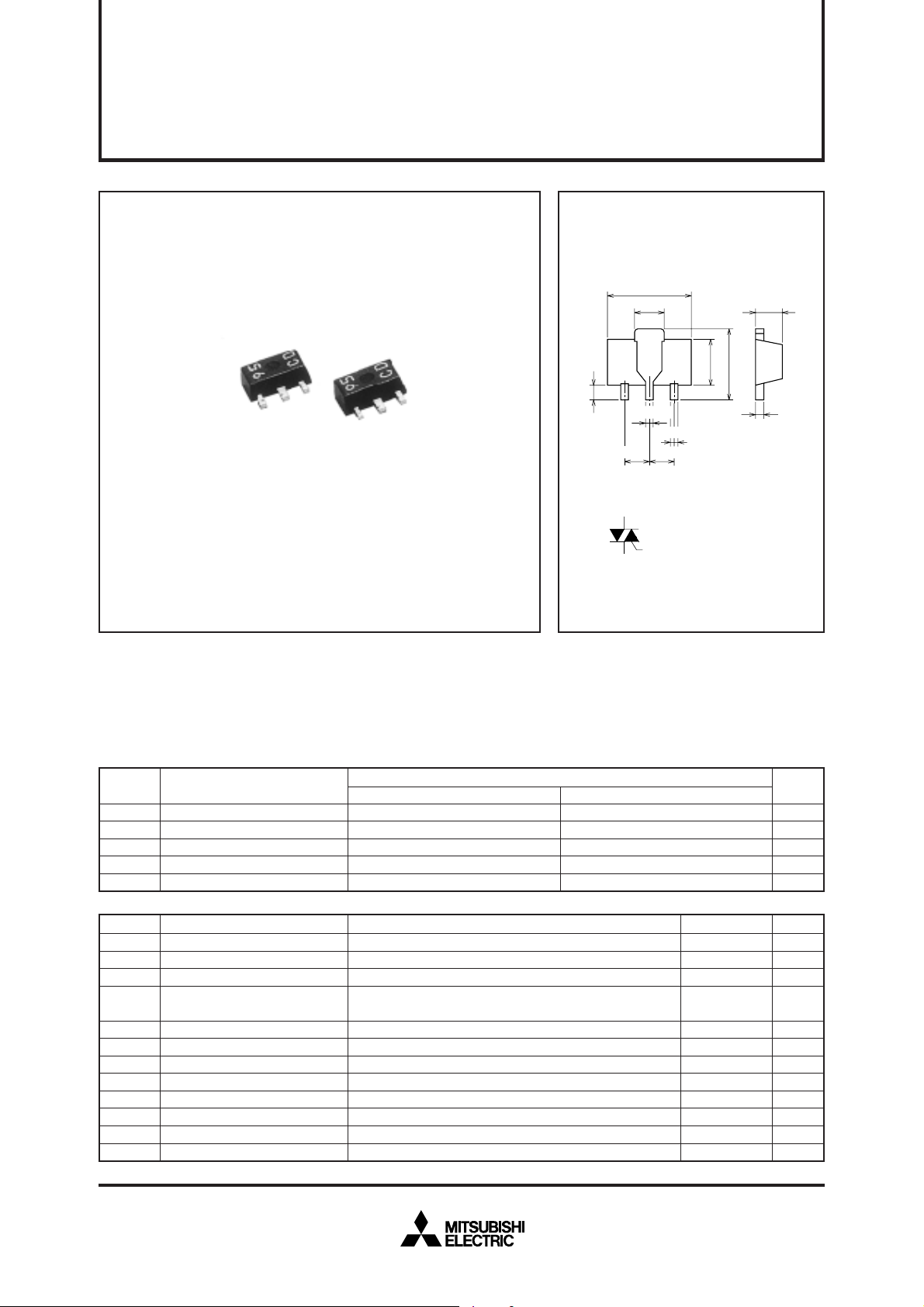
OUTLINE DRAWING
4.4±0.1
1.6±0.2
2
1
0.8 MIN
1.5±0.11.5±0.1
(Back side)
2
1
3
0.5±0.07
0.4±0.07
3
SOT-89
Dimensions
1.5±0.1
2.5±0.1
3.9±0.3
+0.03
0.4
–0.05
T
1
TERMINAL
1
2
TERMINAL
T
2
GATE TERMINAL
3
in mm
APPLICATION
Solid state relay, strobe flasher, ignitor, hybrid IC
MAXIMUM RATINGS
Symbol
RRM
V
VRSM
VR (DC)
VDRM
VD (DC)
Symbol
I
T (RMS)
IT (AV)
ITSM
2
t
I
PGM
PG (AV)
VFGM
VRGM
IFGM
Tj
Tstg
✽1. With Gate-to-cathode resistance RGK=1kΩ
Repetitive peak reverse voltage
Non-repetitive peak reverse voltage
DC reverse voltage
Repetitive peak off-state voltage
DC off-state voltage
RMS on-state current
Average on-state current
Surge on-state current
2
I
t
for fusing
Peak gate power dissipation
Average gate power dissipation
Peak gate forward voltage
Peak gate reverse voltage
Peak gate forward current
Junction temperature
Storage temperature
Weight
—
Parameter
Parameter
4 (marked “CB”)
✽1
✽1
Commercial frequency, sine half wave, 180° conduction, T
60Hz sine half wave 1 full cycle, peak value, non-repetitive
Value corresponding to 1 cycle of half wave 60Hz, surge on-state
current
Typical value
200
300
160
200
160
Conditions
Voltage class
8 (marked “CD”)
400
500
320
400
320
✽2
a=57°C
Ratings
0.79
0.5
10
0.4
0.1
0.01
6
6
0.1
–40 ~ +125
–40 ~ +125
48
Unit
V
V
V
V
V
Unit
A
A
A
2
s
A
W
W
V
V
A
°C
°C
mg
Feb.1999

MITSUBISHI SEMICONDUCTOR 〈THYRISTOR〉
NON-INSULATED TYPE, PLANAR PASSIVATION TYPE
ELECTRICAL CHARACTERISTICS
Symbol
I
RRM
IDRM
VTM
VGT
VGD
IGT
IH
Rth (j-a)
✽2.Soldering with ceramic plate (25mm × 25mm × t0.7).
✽3.If special values of I
The above values do not include the current flowing through the 1kΩ resistance between the gate and cathode.
Repetitive peak reverse current
Repetitive peak off-state current
On-state voltage
Gate trigger voltage
Gate non-trigger voltage
Gate trigger current
Holding current
Thermal resistance
Item
I
GT (µA)
Parameter
j=125°C, VRRM applied
T
T
j=125°C, VDRM applied, RGK=1kΩ
T
a=25°C, ITM=1.5A, instantaneous value
T
a=25°C, VD=6V, IT=0.1A
Tj=125°C, VD=1/2VDRM, RGK=1kΩ
T
j=25°C, VD=6V, IT=0.1A
Tj=25°C, VD=12V, RGK=1kΩ
Junction to ambient
GT are required, choose at least two items from those listed in the table below. (Example: AB, BC)
A
1 ~ 30
B
20 ~ 50
C
40 ~ 100
Test conditions
✽4
✽4
✽2
CR05AS
LOW POWER USE
Limits
Typ.
Min.
—
—
—
—
—
—
—
—
—
0.2
—
1
—
—
—
—
Max.
0.1
0.1
1.9
0.8
—
100
70
Unit
mA
mA
V
V
V
✽3
µA
3
mA
°C/W
GT
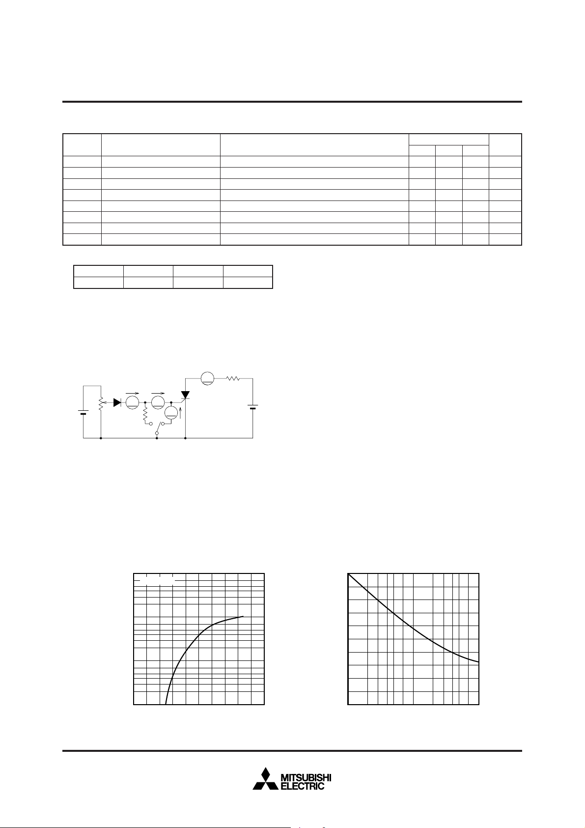
, VGT measurement circuit.
✽4. I
GSIGT
I
3V
DC
A3 A2
GK
R
1kΩ
V1
21
V
GT
SWITCH
SWITCH 1 : IGT measurement
SWITCH 2 : V
GT
measurement
(Inner resistance of voltage meter is about 1kΩ)
PERFORMANCE CURVES
MAXIMUM ON-STATE CHARACTERISTICS
2
10
7
Ta = 25°C
5
3
2
1
10
7
5
3
2
0
10
7
5
ON-STATE CURRENT (A)
3
2
–1
10
TUT
A1
60Ω
6V
DC
RATED SURGE ON-STATE CURRENT
10
9
8
7
6
5
4
3
2
1
SURGE ON-STATE CURRENT (A)
501 423
0
10023 5710
44
1
23 5710
2
ON-STATE VOLTAGE (V)
CONDUCTION TIME
(CYCLES AT 60Hz)
Feb.1999
 Loading...