

Page 1
查询7477 GROUP供应商查询7477 GROUP供应商
DESCRIPTION
The 7477/7478 group is the single-chip microcomputer designed
with CMOS silicon gate technology.
The single-chip microcomputer is useful for business equipment
and other consumer applications.
In addition to its simple instruction set, the ROM, RAM, and I/O
addresses are placed on the same memory map to enable easy
programming.
In addition, built-in PROM type microcomputers with built-in electrically writable PROM, and additional functions equivalent to the
mask ROM version are also available.
7477/7478 group products are shown noted below.
The 7477 and the 7478 differ in the number of I/O ports, package
outline, and clock generating circuit only.
Product
M37477M4-XXXSP/FP
M37477M8-XXXSP/FP
M37477E8SP/FP
M37477E8-XXXSP/FP
M37478M4-XXXSP/FP
M37478M8-XXXSP/FP
M37478E8SP/FP
M37478E8-XXXSP/FP
M37478E8SS
Mask ROM version
One Time PROM version
(Built-in PROM type microcomputers)
Mask ROM version
One Time PROM version
(Built-in PROM type microcomputers)
PROM version
(Built-in PROM type microcomputer)
FEATURES
●Basic machine-language instructions ......................................71
●Memory size
ROM.............................. 8192 bytes (M37477M4, M37478M4)
RAM ................................ 192 bytes (M37477M4, M37478M4)
●The minimum instruction execution time
......................................0.5µs (at 8MHz oscillation frequency)
●Power source voltage
.......... 2.7 to 4.5V (at 2.2VCC – 2.0MHz oscillation frequency)
............................. 4.5 to 5.5V (at 8MHz oscillation frequency)
●Power dissipation in normal mode
.................................... 35mW (at 8MHz oscillation frequency)
●Subroutine nesting
.................................96 levels max. (M37477M4, M37478M4)
●Interrupt ................................................... 13 sources, 11 vectors
●8-bit timers ................................................................................. 4
●Programmable I/O ports
(Ports P0, P1, P4) .......................................... 18 (7477 group)
●Input ports (Ports P2, P3) .................................... 8 (7477 group)
(Ports P2, P3, P5) ............................16 (7478 group)
●8-bit serial I/O ........................... 1 (UART or clock-synchronized)
●8-bit A-D converter ................................ 4 channels (7477 group)
Version
20 (7478 group)
8 channels (7478 group)
MITSUBISHI MICROCOMPUTERS
7477/7478 GROUP
SINGLE-CHIP 8-BIT CMOS MICROCOMPUTER
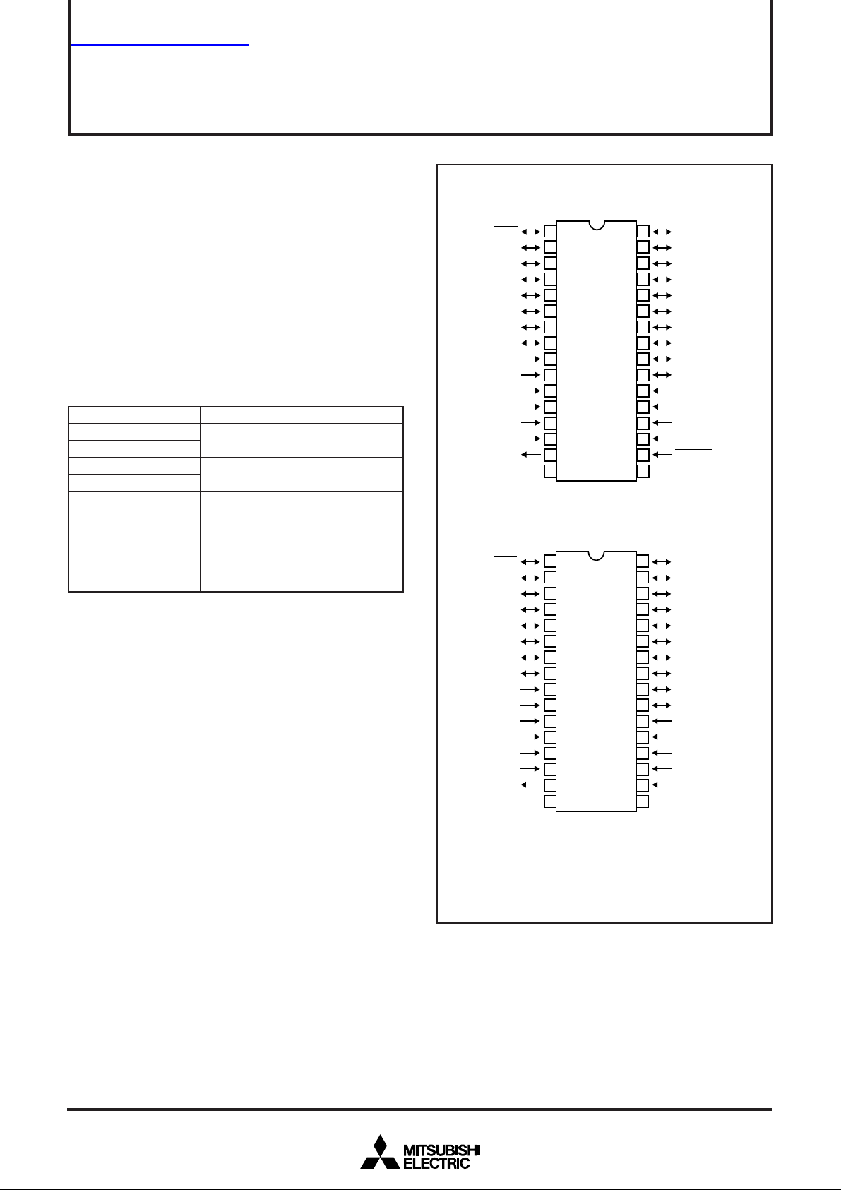
PIN CONFIGURATION (TOP VIEW)
P17/SRDY
P16/SCLK
P15/TXD
P1
4/RXD
P1
3/T1
P12/T0
P11
P10
P23/IN3
P22/IN2
P21/IN1
P20/IN0
VREF
XIN
XOUT
VSS
1
2
3
4
5
M37477E8-XXXSP
6
7
8
9
10
11
12
13
14
15
16
Outline 32P4B
P17/SRDY
P16/SCLK
P15/TXD
P1
4/RXD
P1
3/T1
P12/T0
P11
P10
P23/IN3
P22/IN2
P21/IN1
P20/IN0
VREF
XIN
XOUT
VSS
1
2
3
4
5
M37477E8-XXXFP
6
7
8
9
10
11
12
13
14
15
16 17
Outline 32P2W-A
Note : The only differences between the 32P4B package prod-
uct and the 32P2W-A package product are package
shape and absolute maximum ratings.
APPLICATIONS
Audio-visual equipment, VCR, Tuner,
Office automation equipment
32
P07
31
P06
30
P05
29
P04
28
27
26
25
24
23
22
21
20
19
18
17
32
31
30
29
28
27
26
25
24
23
22
21
20
19
18
P03
P02
P01
P00
P41
P40
P33/CNTR1
P32/CNTR0
P31/INT1
P30/INT0
RESET
CC
V
P07
P06
P05
P04
P03
P02
P01
P00
P41
P40
P33/CNTR1
P32/CNTR0
P31/INT1
P30/INT0
RESET
CC
V
M37477M4-XXXSP
M37477M8-XXXSP
M37477M4-XXXFP
M37477M8-XXXFP
Page 2

PIN CONFIGURATION (TOP VIEW)
P5
3
P17/
S
RDY
P16/S
CLK
P15/TXD
P1
4/RX
D
P1
3/T1
P12/T
0
P1
1
P1
0
P27/IN
7
P26/IN
6
P25/IN
5
P24/IN
4
P23/IN
3
P22/IN
2
P21/IN
1
P20/IN
0
V
REF
X
IN
X
OUT
V
SS
Outline 42P4B
1
2
3
4
5
6
7
M37478E8-XXXSP
M37478E8SS
8
9
10
11
12
13
14
15
16
17
18
19
20
21
42S1B-A (Window)
42
P5
41
P0
40
P0
39
P0
38
P0
37
P0
36
35
34
33
32
31
30
29
28
27
26
25
24
23
22
P0
P0
P0
P4
P4
P4
P4
P33/CNTR
P32/CNTR
P31/INT
P30/INT
RESET
P51/X
P50/X
V
CC
M37478M4-XXXSP
M37478M8-XXXSP
2
7
6
5
4
3
2
1
0
3
2
1
0
COUT
CIN
MITSUBISHI MICROCOMPUTERS
7477/7478 GROUP
SINGLE-CHIP 8-BIT CMOS MICROCOMPUTER
0
1
1
0
/INT
/CNTR
/INT
/CNTR
2
/IN
2
P2
2
P3
32
13
1
/IN
1
P2
1
P3
31
14
0
/IN
0
P2
0
P3
30
15
REF
V
NC
29
16
NC
28
RESET
27
NC
26
P51/X
P50/X
NC
V
CC
V
SS
AV
SS
NC
X
OUT
X
IN
NC
COUT
CIN
25
24
23
22
21
20
19
18
17
3
4
2
P0
P0
NC
P0
43
41
42
44
45
NC
NC
RDY
CLK
NC
46
5
47
6
48
7
49
2
50
51
SS
52
3
53
54
55
56
1
NC
M37478M4-XXXFP
M37478M8-XXXFP
M37478E8-XXXFP
4
3
2
0
1
D
X
/T
/T
2
3
/R
4
P1
P1
P1
P0
P0
P0
P5
V
P5
7
/
S
P1
1
P16/S
0
1
0
P15/TXD
40
5
1
P0
1
P1
0
P0
39
6
0
P1
3
P4
38
7
7
/IN
7
P2
2
P4
37
8
6
/IN
6
P2
36
9
1
P4
5
/IN
5
P2
0P33
P4
NC
35
34
10
11
3
4
/IN
/IN
4
3
P2
P2
33
12
Outline 56P6N-A
Note : The only differences between the 42P4B package product and the 56P6N-A package product are package shape, ab-
solute maximum ratings and the fact that the 56P6N-A package product has an AVSS pin.
2
Page 3
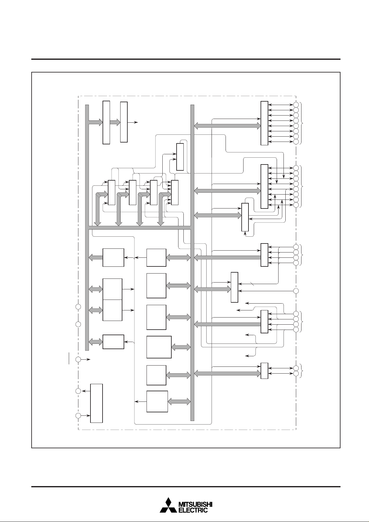
decoder
signal
Control
Instruction
Instruction register(8)
control
MITSUBISHI MICROCOMPUTERS
7477/7478 GROUP
SINGLE-CHIP 8-BIT CMOS MICROCOMPUTER
25
26
27
28
P0
P0(8)
29
I/O port
30
31
32
M37477M4-XXXSP/FP BLOCK DIAGRAM
input
Reset
Clock
output
input
Clock
SS
V
CC
V
RESET
OUT
X
IN
X
Data bus
16
17
18
15
14
(8)
Timer 1
1)
(Note
8192
bytes
(P)ROM
(8)
L
PC
counter
Program
(8)
H
PC
counter
Program
2)
(Note
192
RAM
bytes
circuit
Clock generating
Timer 2(8)
(8)
Timer 3
S(8)
Stack
pointer
Y(8)
Index
register
X(8)
Index
register
status
register
Processor
A(8)
lator
Accumu-
unit
8-bit
Arithmetic
and logical
PS(8)
PWM
(8)
Timer 4
S I/O(8)
4
A-D converter
0
1
INT
INT
0
CNTR
1
CNTR
P1(8)
(4)
P2
P3(4)
(2)
P4
8
7
6
5
P1
4
I/O port
3
2
1
12
11
P2
10
Input port
9
3
REF
1
V
Reference voltage input
19
20
21
P3
22
Input port
23
P4
24
I/O port
2 : 384 bytes for M37477M8/E8-XXXSP/FP
Notes 1 : 16384 bytes for M37477M8/E8-XXXSP/FP
3
Page 4
Control signal
Instruction decoder
Instruction register(8)
MITSUBISHI MICROCOMPUTERS
7477/7478 GROUP
SINGLE-CHIP 8-BIT CMOS MICROCOMPUTER
34
35
36
37
P0(8)
38
39
40
41
I/O port P0
Main clock
M37478M4-XXXSP BLOCK DIAGRAM
SS
V
CC
V
input
Reset
RESET
OUT
X
output
IN
X
input
Main clock
Data bus
21
22
25
20
19
Timer 1(8)
(Note 1)
8192
bytes
(P)ROM
(8)
L
PC
counter
Program
(8)
H
PC
counter
Program
(Note 2)
192
RAM
bytes
COUT
X
Sub-clock
circuit
CIN
Clock generating
X
Sub-clock
output
input
Timer 2(8)
Timer 3(8)
S(8)
Stack
pointer
Y(8)
Index
register
X(8)
Index
register
PS(8)
status
register
Processor
A(8)
lator
Accumu-
unit
8-bit
Arithmetic
and logical
PWM control
Timer 4(8)
S I/O(8)
8
A-D converter
0
INT
1
INT
0
CNTR
1
CNTR
CIN
X
COUT
X
P1(8)
P2(8)
P3(4)
P4(4)
P5(4)
9
8
7
6
5
4
I/O port P1
3
2
17
16
15
14
13
12
Input port P2
11
10
REF
18
V
Reference voltage input
26
27
28
29
Input port P3
30
31
32
33
I/O port P4
23
24
42
1
Input port P5
Notes 1 : 16384 bytes for M37478M8/E8-XXXSP, M37478E8SS
2 : 384 bytes for M37478M8/E8-XXXSP, M37478E8SS
4
Page 5

Control signal
Instruction decoder
Instruction register(8)
MITSUBISHI MICROCOMPUTERS
7477/7478 GROUP
SINGLE-CHIP 8-BIT CMOS MICROCOMPUTER
39
40
41
42
P0(8)
43
46
47
48
I/O port P0
M37478M4-XXXFP BLOCK DIAGRAM
21
AVSS
VSS
22
23
VCC
input
Reset
RESET
OUT
X
output
Main clock
IN
18
X
input
Main clock
Data bus
51
28
19
Timer 1(8)
(Note 1)
8192
bytes
(P)ROM
L(8)
PC
counter
Program
H(8)
PC
counter
Program
(Note 2)
192
RAM
bytes
XCOUT
Sub-clock
circuit
CIN
Clock generating
X
Sub-clock
output
input
Timer 2(8)
Timer 3(8)
S(8)
Stack
pointer
Y(8)
Index
register
X(8)
Index
register
PS(8)
status
register
Processor
A(8)
lator
Accumu-
unit
8-bit
Arithmetic
and logical
PWM control
Timer 4(8)
S I/O(8)
8
A-D converter
INT0
INT1
CNTR0
CNTR1
XCIN
XCOUT
P1(8)
P2(8)
P3(4)
P4(4)
P5(4)
6
5
4
3
2
55
I/O port P1
54
53
14
13
12
11
10
9
Input port P2
8
7
REF
15
V
Reference voltage input
30
31
32
33
Input port P3
35
36
37
38
I/O port P4
25
26
49
52
Input port P5
Notes 1 : 16384 bytes for M37478M8/E8-XXXFP
2 : 384 bytes for M37478M8/E8-XXXFP
5
Page 6
FUNCTIONS OF 7477/7478 GROUP
MITSUBISHI MICROCOMPUTERS
7477/7478 GROUP
SINGLE-CHIP 8-BIT CMOS MICROCOMPUTER
Parameter
Basic machine-language instructions
Instruction execution time
Clock input oscillation frequency
M37477M4
Memory size
Input/Output port
Serial I/O
Timers
A-D converter
Subroutine nesting
Interrupt
Clock generating circuit
Power source circuit
Power dissipation
Input/Output characters
Operating temperature range
Device structure
Package
M37478M4
M37477M8/E8
M37478M8/E8
P0, P1
P2
P3, P5
P4
M37477M4, M37478M4
M37477M8/E8, M37478M8/E8
Input/Output voltage
Output current
M37477M4/M8/E8-XXXSP
M37477M4/M8/E8-XXXFP
M37478M4/M8/E8-XXXSP
M37478M4/M8/E8-XXXFP
M37478E8SS
ROM
RAM
(P)ROM
RAM
I/O
Input
Input
I/O
Functions
71
0.5µs (The minimum instructions, at 8 MHz oscillation frequency)
8 MHz (max.)
8192 bytes
192 bytes
16384 bytes
384 bytes
8-bit ✕ 2
8-bit ✕ 1 (4-bit ✕ 1 for the 7477 group)
4-bit ✕ 2 (Port P5 is not included in the 7477 group)
4-bit ✕ 1 (2-bit ✕ 1 for the 7477 group)
8-bit ✕ 1
8-bit timer ✕ 4
8-bit ✕ 1 (8 channels) (8-bit ✕ 1 (4 channels) for the 7477 group)
96 (max.)
192 (max.)
5 external interrupts, 7 internal interrupts, 1 software interrupt
Built-in circuit with internal feedback resistor (a ceramic or a quartz-
crystal oscillator)
2.7 to 4.5V (at 2.2VCC–2.0MHz oscillation frequency), 4.5 to 5.5V
(at 8MHz oscillation frequency)
35mW (at 8MHz oscillation frequency)
5V
–5 to 10mA (P0, P1, P4 : CMOS tri-states)
–20 to 85°C
CMOS silicon gate
32-pin shrink plastic molded DIP
32-pin plastic molded SOP
42-pin shrink plastic molded DIP
56-pin plastic molded QFP
42-pin ceramic DIP
6
Page 7
PIN DESCRIPTION
MITSUBISHI MICROCOMPUTERS
7477/7478 GROUP
SINGLE-CHIP 8-BIT CMOS MICROCOMPUTER
Pin Name Functions
VCC, VSS
AVSS
(Note 1)
RESET
XIN
XOUT
VREF
P00 – P07
P10 – P17
P20 – P27
(Note 2)
P30 – P33
P40 – P43
(Note 3)
P50 – P53
(Note 4)
Notes 1 : AV
2 : Only P20–P23 (IN0–IN3) 4-bit for the 7477 group.
3 : Only P40 and P41 2-bit for the 7477 group.
4 : This port is not included in the 7477 group.
Power source
Analog power
source
Reset input
Clock input
Clock output
Reference voltage
input
I/O port P0
I/O port P1
Input port P2
Input port P3
I/O port P4
Input port P5
SS for M37478M4/M8/E8-XXXFP.
Input/
Output
Input
Input
Output
Input
I/O
I/O
Input
Input
I/O
Input
Apply voltage of 2.7 to 5.5V to VCC, and 0V to VSS.
Ground level input pin for A-D converter.
Same voltage as VSS is applied.
To enter the reset state, the reset input pin must be kept at “L” for 2µs or more
(under normal VCC conditions).
These are I/O pins of internal clock generating circuit for main clock. To
control generating frequency, an external ceramic or a quartz crystal oscillator
is connected between the X
clock source should be connected the XIN pin and the XOUT pin should be left
open. Feedback resistor is connected between XIN and XOUT.
Reference voltage input pin for A-D converter.
Port P0 is an 8-bit I/O port. The output structure is CMOS output.
When this port is selected for input, pull-up transistor can be connected in
units of 1-bit and a key on wake up function is provided.
Port P1 is an 8-bit I/O port. The output structure is CMOS output.
When this port is selected for input, pull-up transistor can be connected in
units of 4-bit. P1
P14, P15, P16 and P17 are in common with serial I/O pins RXD, TXD, SCLK
____
and SRDY, respectively .
Port P2 is an 8-bit input port.
This port is in common with analog input pins IN0 to IN7.
Port P3 is a 4-bit input port. P30, P31 are in common with external interrupt
input pins INT0, INT1, and P32, P33 are in common with timer input pins
CNTR0, CNTR1.
Port P4 is a 4-bit I/O port. The output structure is CMOS output, When this
port is selected for input, pull-up transistor can be connected in units of 4-bit.
Port P5 is a 4-bit input port and pull-up transistor can be connected in units of
4-bit. P50, P51 are in common with input/output pins of clock for clock function
XCIN, XCOUT. When P50, P51 are used as XCIN, XCOUT, connect a ceramic or a
quartz crystal oscillator between XCIN and XCOUT. If an external clock input is
used, connect the clock input to the XCIN pin and open the XCOUT pin.
Feedback resistor is connected between XCIN and XCOUT pins.
2 and P13 are in common with timer output pins T0 and T1.
IN and XOUT pins. If an external clock is used, the
7
Page 8
MITSUBISHI MICROCOMPUTERS
7477/7478 GROUP
SINGLE-CHIP 8-BIT CMOS MICROCOMPUTER
FUNCTIONAL DESCRIPTION
Central Processing Unit (CPU)
The 7477/7478 group uses the standard 740 family instruction set.
Refer to the table of 740 family addressing modes and machine instructions or the SERIES 740 <Software> User’s Manual for
details on the instruction set.
Machine-resident 740 family instructions are as follows:
The FST and SLW instruction cannot be used.
The MUL, DIV, WIT, and STP instruction can be used.
b7
CPU Mode Register
The CPU mode register is allocated at address 00FB16.
This register contains the stack page selection bit.
b0
CPU mode register (Address 00FB16)
These bits must always be set to “0”.
Stack page selection bit (Note 1)
0 : In page 0 area
1 : In page 1 area
Notes 1 : In the M37477M4-XXXSP/FP, M37478M4-XXXSP/FP, set this bit to “0”.
2 : In the 7477 group, set this bit to “0”.
Fig. 1 Structure of CPU mode register
0
, P51/X
CIN
, X
COUT
P5
0 : P5
1 : X
X
0 : Low
1 : High
Clock (XIN-X
0 : Oscillates
1 : Stops
Internal system clock selection bit (Note 2)
0 : X
1 : X
0
, P5
1
CIN
, X
COUT
COUT
drive capacity selection bit (Note 2)
OUT
IN-XOUT
CIN-XCOUT
selection bit (Note 2)
) stop bit (Note 2)
selected (normal mode)
selected (low-speed mode)
8
Page 9
MITSUBISHI MICROCOMPUTERS
7477/7478 GROUP
SINGLE-CHIP 8-BIT CMOS MICROCOMPUTER
MEMORY
• Special Function Register (SFR) Area
The special function register (SFR) area contains the registers
relating to functions such as I/O ports and timers.
• RAM
RAM is used for data storage as well as a stack area.
• ROM
ROM is used for storing user programs as well as the interrupt
vector area.
RAM (192 bytes)
for
M37477M4
M37477M8/E8
M37478M4
M37478M8/E8
RAM (192 bytes)
for
M37477M8/E8
M37478M8/E8
• Interrupt Vector Area
The interrupt vector area is for storing jump destination addresses used at reset or when an interrupt is generated.
• Zero Page
Zero page addressing mode is useful because it enables access
to this area with fewer instruction cycles.
• Special Page
Special page addressing mode is useful because it enables access to this area with fewer instruction cycles.
16
0000
Zero
page
00BF16
00FF16
010016
01BF16
SFR area
Fig. 2 Memory map
ROM (16K bytes)
for
M37477M8/E8
M37478M8/E8
ROM (8K bytes)
for
M37477M4
M37478M4
C00016
E00016
FF0016
FFE816
FFFF16
Not used
Special
page
Interrupt vector area
9
Page 10
MITSUBISHI MICROCOMPUTERS
7477/7478 GROUP
SINGLE-CHIP 8-BIT CMOS MICROCOMPUTER
00C016
00C116
00C216
00C316
00C416
00C516
00C616
00C716
00C816
00C916
00CA16
00CB16
00CC16
00CD16
00CE16
00CF16
00D016
00D116
00D216
00D316
00D416
00D516
00D616
00D716
00D816
00D916
00DA16
00DB16
00DC16
00DD16
00DE16
00DF16
Port P0
Port P0 direction register
Port P1
Port P1 direction register
Port P2
Port P3
Port P4
Port P4 direction register
Port P5 (Note 1)
P0 pull-up control register
P1–P5 pull-up control register (Note 2)
Edge polarity selection register
Input latch register
A-D control register
A-D conversion register
00E016
00E116
00E216
00E316
00E416
00E516
00E616
00E716
00E816
00E916
00EA16
00EB16
00EC16
00ED16
00EE16
00EF16
00F016
00F116
00F216
00F316
00F416
00F516
00F616
00F716
00F816
00F916
00FA16
00FB16
00FC16
00FD16
00FE16
00FF16
Transmit/receive buffer register
Serial I/O status register
Serial I/O control register
UART control register
Baud rate generator
Timer 1
Timer 2
Timer 3
Timer 4
Timer FF register
Timer 12 mode register
Timer 34 mode register
Timer mode register 2
CPU mode register
Interrupt request register 1
Interrupt request register 2
Interrupt control register 1
Interrupt control register 2
Notes 1 : This address is not used in the 7477 group.
2 : This address is allocated P1–P4 pull-up control register for the 7477 group.
Fig. 3 SFR (Special Function Register) memory map
10
Page 11
MITSUBISHI MICROCOMPUTERS
7477/7478 GROUP
SINGLE-CHIP 8-BIT CMOS MICROCOMPUTER
INTERRUPTS
Interrupts can be caused by 13 different sources consisting of five
external, seven internal, and one software sources.
Interrupts are vectored interrupts with priorities shown in Table 1.
Reset is also included in the table because its operation is similar
to an interrupt.
When an interrupt is accepted, the registers are pushed, interrupt
disable flag I is set, and the program jumps to the address specified in the vector table. The interrupt request bit is cleared
automatically. The reset and BRK instruction interrupt can never
be disabled. Other interrupts are disabled when the interrupt disable flag is set.
All interrupts except the BRK instruction interrupt have an interrupt
request bit and an interrupt enable bit. The interrupt request bits
are in interrupt request registers 1 and 2 and the interrupt enable
bits are in interrupt control registers 1 and 2. External interrupts
INT0 and INT1 can be asserted on either the falling or rising edge
as set in the edge polarity selection register. When “0” is set to this
register, the interrupt is activated on the falling edge; when “1” is
set to the register, the interrupt is activated on the rising edge.
When the device is put into power-down state by the STP instruction or the WIT instruction, if bit 5 in the edge polarity selection
register is “1”, the INT1 interrupt becomes a key on wake up interrupt. When a key on wake up interrupt is valid, an interrupt request
is generated by applying the “L” level to any pin in port P0. In this
case , the port used for interrupt must have been set for the input
mode.
If bit 5 in the edge polarity selection register is “0” when the device
is in power-down state, the INT1 interrupt is selected. Also, if bit 5
in the edge polarity selection register is set to “1” when the device
is not in a power-down state, neither key on wake up interrupt request nor INT1 interrupt request is generated.
The CNTR0/CNTR1 interrupts function in the same as INT0 and
INT1. The interrupt input pin can be specified for either CNTR0 or
CNTR1 pin by setting bit 4 in the edge polarity selection register.
Figure 4 shows the structure of the edge polarity selection register, interrupt request registers 1 and 2, and interrupt control
registers 1 and 2.
Interrupts other than the BRK instruction interrupt and reset are
accepted when the interrupt enable bit is “1”, interrupt request bit
is “1”, and the interrupt disable flag is “0”. The interrupt request bit
can be reset with a program, but not set. The interrupt enable bit
can be set and reset with a program.
Reset is treated as a non-maskable interrupt with the highest priority. Figure 5 shows interrupts control.
Table 1. Interrupt vector address and priority.
______
RESET
INT0 interrupt
INT1 interrupt or key on wake up interrupt
CNTR0 interrupt or CNTR1 interrupt
Timer 1 interrupt
Timer 2 interrupt
Timer 3 interrupt
Timer 4 interrupt
Serial I/O receive interrupt
Serial I/O transmit interrupt
A-D conversion completion interrupt
BRK instruction interrupt
Interrupt source
Priority
1
2
3
4
5
6
7
8
9
10
11
12
Vector addresses
FFFF16, FFFE16
FFFD16, FFFC16
FFFB16, FFFA16
FFF916, FFF816
FFF716, FFF616
FFF516, FFF416
FFF316, FFF216
FFF116, FFF016
FFEF16, FFEE16
FFED16, FFEC16
FFEB16, FFEA16
FFE916, FFE816
Remarks
Non-maskable
External interrupt (polarity programmable)
External interrupt (INT1 is polarity programmable)
External interrupt (polarity programmable)
Non-maskable software interrupt
11
Page 12
MITSUBISHI MICROCOMPUTERS
7477/7478 GROUP
SINGLE-CHIP 8-BIT CMOS MICROCOMPUTER
b7 b0
b7 b0
Edge polarity selection register (EG)
(Address 00D4
INT0 edge selection bit
INT
1 edge selection bit
CNTR
0 edge selection bit
CNTR
1 edge selection bit
0 : Falling edge
1 : Rising edge
CNTR
0/CNTR1 interrupt selection bit
0 : CNTR
1 : CNTR
INT1 source selection bit (at power-down state)
0 : P3
1 : P0
Nothing is allocated (The value is undefined at reading)
Interrupt request register 1
(Address 00FC
Timer 1 interrupt request bit
Timer 2 interrupt request bit
Timer 3 interrupt request bit
Timer 4 interrupt request bit
Nothing is allocated
(The value is undefined at reading)
Serial I/O receive interrupt request bit
Serial I/O transmit interrupt request bit
A-D conversion completion interrupt request bit
16)
0
1
1/INT1
0 – P07 “L” level (for key-on wake-up)
16)
b7 b0
Interrupt request register 2
(Address 00FD
INT0 interrupt request bit
INT
1 interrupt request bit
CNTR0 or CNTR1 interrupt request bit
0 : No interrupt request
1 : Interrupt requested
Nothing is allocated
(The value is undefined at reading)
16)
b7 b0
Interrupt control register 1
(Address 00FE
Timer 1 interrupt enable bit
Timer 2 interrupt enable bit
Timer 3 interrupt enable bit
Timer 4 interrupt enable bit
Nothing is allocated
(The value is undefined at reading)
Serial I/O receive interrupt enable bit
Serial I/O transmit interrupt enable bit
A-D conversion completion interrupt enable bit
Fig. 4 Structure of registers related to interrupt
Interrupt request bit
Interrupt enable bit
Interrupt disable flag I
BRK instruction
Reset
16)
b7
b0
Interrupt control register 2
(Address 00FF
INT0 interrupt enable bit
INT
1 interrupt enable bit
CNTR0 or CNTR1 interrupt enable bit
0 : Interrupt disable
1 : Interrupt enabled
Nothing is allocated
(The value is undefined at reading)
16)
Interrupt request
Fig. 5 Interrupt control
12
Page 13

MITSUBISHI MICROCOMPUTERS
7477/7478 GROUP
SINGLE-CHIP 8-BIT CMOS MICROCOMPUTER
TIMER
The 7477/7478 group has four timers; timer 1, timer 2, timer 3,
and timer 4.
A block diagram of timer 1 through 4 is shown in Figure 6.
Timer 1 can be operated in the timer mode, event count mode, or
pulse output mode. Timer 1 starts counting when bit 0 in the timer
12 mode register (address 00F816) is set to “0”.
The count source can be selected from the f(XIN) divided by 16,
f(XCIN) divided by 16, f(XCIN), or event input from P32/CNTR0 pin.
Do not select f(XCIN) as the count source in the 7477 group. When
bit 1 and bit 2 in the timer 12 mode register are “0”, f(XIN) divided
by 16 or f(XCIN) divided by 16 is selected. Selection between
f(XIN) and f(XCIN) is done by bit 7 in the CPU mode register (address 00FB16). When bit 1 in the timer 12 mode register is “0” and
bit 2 is “1”, f(XCIN) is selected. And, when bit 1 in the timer 12
mode register is “1”, an event input from the CNTR0 pin is selected. Event inputs are selected depending on bit 2 in the edge
polarity selection register (address 00D416). When this bit is “0”,
the inverted value of CNTR0 input is selected; when the bit is “1”,
CNTR0 input is selected.
When bit 3 in the timer 12 mode register is set to “1”, the P12 pin
becomes timer output T0. When the direction register of P12 is set
for the output mode at this time, the timer 1 overflow divided by 2
is output from T0.
Please set the initial output value in the following procedure.
➀ Set “1” to bit 0 of the timer 12 mode register.
(Timer 1 count stop.)
➁ Set “1” to bit 0 of the timer mode register 2.
➂ Set the output value to bit 0 of the timer FF register.
➃ Set the count value to the timer 1.
➄ Set “0” to bit 0 of the timer 12 mode register.
(Timer 1 count start.)
Timer 2 can only be operated in the timer mode. Timer 2 starts
counting when bit 4 in the timer 12 mode register is set to “0”.
The count source can be selected from the divide by 16, divide by
64, divide by 128, or divide by 256 frequency of f(XIN) or f(XCIN),
and timer 1 overflow. Do not select f(XCIN) as the count source in
the 7477 group. When bit 5 in the timer 12 mode register is “0”,
any of the divide by 16, divide by 64, divide by 128, or divide by
256 frequency of f(XIN) or f(XCIN) is selected. The divide ratio is
selected according to bit 6 and bit 7 in the timer 12 mode register,
and selection between f(XIN) and f(XCIN) is made according to bit
7 in the CPU mode register. When bit 5 in the timer 12 mode register is “1”, timer 1 overflow is selected as the count source.
Timer 3 can be operated in the timer mode, event count mode, or
PWM mode. Timer 3 starts counting when bit 0 in the timer 34
mode register (address 00F916) is set to “0”.
The count source can be selected from the f(XIN) divided by 16,
f(XCIN) divided by 16, f(XCIN), timer 1 or timer 2 overflow, or an
event input from P33/CNTR1 pins according to the statuses of bit 1
and bit 2 in the timer 34 mode register, bit 6 in the timer mode register 2 (address 00FA16) and bit 7 in the CPU mode register. Do
not select f(XCIN) as the count source in the 7477 group. Note,
however, that if timer 1 overflow or timer 2 overflow is selected for
the count source of timer 3 when timer 1 overflow is selected for
the count source of timer 2, timer 1 overflow is always selected regardless of the status of bit 6 in the timer mode register 2. Event
inputs are selected depending on bit 3 in the edge polarity selection register. When this bit is “0”, the inverted value of CNTR1 input
is selected; when the bit is “1”, CNTR1 input is selected.
Timer 4 can be operated in the timer mode, event count mode,
pulse output mode, pulse width measuring mode, or PWM mode.
Timer 4 starts counting when bit 3 in the timer 34 mode register is
set to “0” when bit 6 in this register is “0”. When bit 6 is “1”, the
pulse width measuring mode is selected. The count source can be
selected from timer 3 overflow, f(XIN) divided by 16, f(XCIN) divided
by 16, f(XCIN), timer 1 or timer 2 overflow, or an event input from
P33/CNTR1 pin according to the statuses of bit 4 and bit 5 in the
timer 34 mode register, bit 6 in the timer mode register 2, and bit 7
in the CPU mode register. Do not select f(XCIN) as the count
source in the 7477 group. Note, however, that if timer 1 overflow or
timer 2 overflow is selected for the count source of timer 4 when
timer 1 overflow is selected for the count source of timer 2, timer 1
overflow is always selected regardless of the status of bit 6 in the
timer mode register 2. Event inputs are selected depending on bit
3 in the edge polarity selection register.
When this bit is “0”, the inverted value of CNTR1 input is selected;
when the bit is “1”, CNTR1 input is selected.
When bit 7 in the timer 34 mode register is set to “1”, the P13 pin
becomes timer output T1. When the direction register of P13 is set
for the output mode at this time, the timer 4 overflow divided by 2
is output from T1 when bit 7 in the timer mode register 2 is “0”.
Please set the initial output value in the following procedure.
➀ Set “1” to bit 3 of the timer 34 mode register.
(Timer 4 count stop.)
➁ Set “1” to bit 1 of the timer mode register 2.
➂ Set the output value to bit 1 of the timer FF register.
➃ Set the count value to the timer 4.
➄ Set “0” to bit 3 of the timer 34 mode register.
(Timer 4 count start.)
(1) Timer mode
Timer performs down count operations with the dividing ratio being
1/(n+1). Writing a value to the timer latch sets a value to the timer.
When the value to be set to the timer latch is nn16, the value to be
set to a timer is nn16, which is down counted at the falling edge of
the count source from nn16 to (nn16-1) to (nn16-2) to ...0116 to 0016
to FF16. At the falling edge of the count source immediately after
timer value has reached FF16, value (nn16-1) obtained by subtracting one from the timer latch value is set (reloaded) to the timer to
continue counting. At the rising edge of the count source immediately after the timer value has reached FF16, an overflow occurs
and an interrupt request is generated.
(2) Event count mode
Timer operates in the same way as in the timer mode except that
it counts input from the CNTR0 or CNTR1 pin.
(3) Pulse output mode
In this mode, duty 50% pulses are output from the T0 or T1 pin.
When the timer overflows, the polarity of the T0 or T1 pin output
level is inverted.
(4) Pulse width measuring mode
The 7477/7478 group can measure the “H” or “L” width of the
CNTR0 or CNTR1 input waveform by using the pulse width measuring mode of timer 4. The pulse width measuring mode is
selected by writing “1” to bit 6 in the timer 34 mode register. In the
pulse width measuring mode, the timer counts the count source
while the CNTR0 or CNTR1 input is “H” or “L”. Whether the CNTR0
input or CNTR1 input to be measured can be specified by the status of bit 4 in the edge polarity selection register; whether the “H”
13
Page 14

MITSUBISHI MICROCOMPUTERS
7477/7478 GROUP
SINGLE-CHIP 8-BIT CMOS MICROCOMPUTER
width or “L” width to be measured can be specified by the status of
bit 2 (CNTR0) and bit 3 (CNTR1) in the edge polarity selection register.
(5) PWM mode
The PWM mode can be entered for timer 3 and timer 4 by setting
bit 7 in the timer mode register 2 to “1”. In the PWM mode, the P13
pin is set for timer output T1 to output PWM waveforms by setting
bit 7 in the timer 34 mode register to “1”. The direction register of
P13 must be set for the output mode before this can be done.
In the PWM mode, timer 3 is counting and timer 4 is idle while the
PWM waveform is “L”. When timer 3 overflows, the PWM waveform goes “H”. At this time, timer 3 stops counting simultaneously
and timer 4 starts counting. When timer 4 overflows, the PWM
waveform goes “L”, and timer 4 stops and timer 3 starts counting
again. Consequently, the “L” duration of the PWM waveform is determined by the value of timer 3; the “H” duration of the PWM
waveform is determined by the value of timer 4.
When a value is written to the timer in operation during the PWM
mode, the value is only written to the timer latch, and not written to
the timer. In this case, if the timer overflows, a value one less the
value in the timer latch is written to the timer. When any value is
written to an idle timer, the value is written to both the timer latch
and the timer.
In this mode, do not select timer 3 overflow as the count source for
timer 4.
INPUT LATCH FUNCTION
The 7477/7478 group can latch the P30/INT0, P31/INT1, P32/
CNTR0, and P33/CNTR1 pin level into the input latch register (address 00D616) when timer 4 overflows. The polarity of each pin
latched to the input latch register can be selected by using the
edge polarity selection register.
When bit 0 in the edge polarity selection register is “0”, the inverted value of the P30/INT0 pin level is latched; when the bit is
“1”, the P30/INT0 pin level is latched as it is.
When bit 1 in the edge polarity selection register is “0”, the inverted value of the P31/INT1 pin level is latched; when the bit is
“1”, the P31/INT1 pin level is latched as it is. When bit 2 in the
edge polarity selection register is “0”, the inverted value of the
P32/CNTR0 pin level is latched; when the bit is “1“, the P32/CNTR0
pin level is latched as it is. When bit 3 in the edge polarity selection register is “0”, the inverted value of the P33/CNTR1 pin level is
latched; when the bit is “1”, the P33/CNTR1 pin level is latched as
it is.
14
Page 15
X
CIN
(Note)
MITSUBISHI MICROCOMPUTERS
7477/7478 GROUP
SINGLE-CHIP 8-BIT CMOS MICROCOMPUTER
Data bus
1/2
P32/CNTR
P12/T
P32/CNTR
T12M
X
1/2
IN
0
Port latch
0
CM
T12M
7
EG
3
1/8
2
T12M
2
T12M
1
TM2
Timer 1 latch (8)
0
0
1/2
Timer 1 (8)
Timer 1
interrupt request
Timer 2 latch (8)
T12M
1/4
1/8
1/16
T12M
6
7
T12M
5
TM2
T12M
6
T34M
T34M
4
Timer 2 (8)
1
2
Timer 2
interrupt request
Timer 3 latch (8)
T34M
0
1
EG
3
T34M
4
T34M
5
Timer 3 (8)
Timer 3
interrupt request
Timer 4 latch (8)
Port latch
P13/T
1
T34M
( Select gate : At reset, shaded side is connected.)
Note : The 7477 group does not have X
Fig. 6 Block diagram of timer 1 through 4
EG
7
P33/CNTR
P32/CNTR
P31/INT
P30/INT
T34M
4
1
0
1
0
6
T34M
Timer 4 (8)
3
F/F
Timer 4
interrupt request
1/2
TM2
7
TM2
EG
EG
3
2
1
C
D3 Q3
EG
1
D2 Q2
D1 Q1
D0 Q0
EG
0
CIN
input.
15
Page 16

MITSUBISHI MICROCOMPUTERS
7477/7478 GROUP
SINGLE-CHIP 8-BIT CMOS MICROCOMPUTER
b7 b0
b7 b0
Timer mode register 2 (TM2)
16
(Address 00FA
)
Timer 1 overflow FF set enable bit
0 : Set disable
1 : Set enable
Timer 4 overflow FF set enable bit
0 : Set disable
1 : Set enable
Nothing is allocated
(The value is undefined at reading)
Timer 3, timer 4 count overflow signal
selection bit
0 : Timer 1 overflow
1 : Timer 2 overflow
Timer 3, timer 4 function selection bit
0 : Normal mode
1 : PWM mode
Timer 12 mode register (T12M)
16
(Address 00F8
)
Timer 1 count stop bit
0 : Count start
1 : Count stop
Timer 1 count source selection bit
0 : Internal clock (Note 1)
1 : P3
2
/CNTR0 external clock
Timer 1 internal clock source
selection bit (Note 2)
0 : f(X
IN
) divided by 16 or
f(X
CIN
CIN
)
1 : f(X
P1
2/T0
port output selection bit
2
port output
0 : P1
) divided by 16
1 : Timer 1 overflow divided by 2
Timer 2 count stop bit
0 : Count start
1 : Count stop
Timer 2 count source selection bit
0 : Internal clock
1 : Timer 1 overflow
Timer 2 internal clock source
selection bits (Note 3)
00 : f(X
IN
) divided by 16 or
f(X
CIN
01 : f(X
10 : f(X
11 : f(X
IN
) divided by 64 or
IN
) divided by 128 or
IN
) divided by 256 or
) divided by 16
f(X
CIN
) divided by 64
f(X
CIN
) divided by 128
f(X
CIN
) divided by 256
b7 b0
Timer 34 mode register (T34M)
16
(Address 00F9
)
Timer 3 count stop bit
0 : Count start
1 : Count stop
Timer 3 count source selection bits (Note 3)
00 : f(X
IN
) divided by 16 or
f(X
CIN
01 : f(X
CIN
)
) divided by 16
10 : Timer 1 overflow or timer 2 overflow
11 : P3
3
/CNTR1 external clock
Timer 4 count stop bit
0 : Count start
1 : Count stop
Timer 4 count source selection bits (Note 3)
00 : Timer 3 overflow
01 : f(X
IN
) divided by 16 or
f(X
CIN
) divided by 16
10 : Timer 1 overflow or timer 2 overflow
11 : P3
3
/CNTR1 external clock
Timer 4 pulse width measuring mode
selection bit
0 : Timer mode
1 : Pulse width measuring mode
P1
3/T1
port output selection bit
0 : P1
3
port output
1 : Timer 4 overflow divided by 2
or PWM output
IN
Notes 1 : f(X
) divided by 16 in the 7477 group.
2 : The 7477 group does not use this bit (bit 2). Set this bit to “0”.
3 : Do not select f(X
CIN
) as the count source in the 7477 group.
Fig. 7 Structure of timer mode registers
16
Page 17

MITSUBISHI MICROCOMPUTERS
7477/7478 GROUP
SINGLE-CHIP 8-BIT CMOS MICROCOMPUTER
SERIAL I/O
Serial I/O can be used as either clock synchronous or asynchronous (UART) serial I/O. A dedicated timer (baud rate generator) is
also provided for baud rate generation.
Address 00E0
Shift clock
CSS
Baud rate generator
Shift clock
Address 00E0
RXD
S
CLK
f(X
S
RDY
TXD
P1
P1
6
4
Receive buffer register
Receive shift register
RE
SIOE
IN
)
1/4
1/4
SRDY
P1
F/F
TE
P1
7
Fall detect
Transmit shift register
Transmit buffer register
5
Clock Synchronous Serial I/O Mode
Clock synchronous serial I/O mode can be selected by setting the
mode selection bit of the serial I/O control register to “1”.
For clock synchronous serial I/O, the transmitter and the receiver
must use the same clock. If an internal clock is used, transfer is
started by a write signal to the transmit or receive buffer.
Data bus
16
Frequency dividing
ratio 1/(n+1)
Address 00E4
TIC
16
Serial I/O control register
Receive buffer full flag (RBF)
Receive interrupt request (RI)
Clock control circuit
Serial I/O synchronous
clock selection
bit (SCS)
1/4
16
Clock control circuit
Transmit shift completion flag (TSC)
Transmit interrupt request (TI)
Transmit buffer empty flag (TBE)
Serial I/O status register
Address 00E2
Address 00E1
16
16
Fig. 8 Clock synchronous serial I/O block diagram
Transfer shift clock
(1/8 to 1/8192 of the internal
clock, or an external clock)
Serial output TxD
Serial input RxD
Receive enable signal S
Write signal to
receive/transmit buffer
Notes 1 : The transmit interrupt request (TI) can be selected to occur either when the transmit buffer has emptied (TBE = 1) or after the
RDY
TBE = 0
transmit shift operation has ended (TSC = 1), by setting the transmit interrupt source selection bit (TIC) of the serial I/O control
register.
2 : If data is written to the transmit buffer when TSC = 0, the transmit clock is generated continuously and serial data is output
continuously from the TxD pin.
3 : The receive interrupt request (RI) is set when the receive buffer full flag (RBF) becomes “1”.
D0 D1 D2 D3 D4 D5 D6
D0 D1 D2 D3 D4 D5
TBE = 1
TSC = 0
Fig. 9 Operation of clock synchronous serial I/O function
Data bus
D7
D6
Overrun error (OE) detection
D7
RBF = 1
TSC = 1
17
Page 18

MITSUBISHI MICROCOMPUTERS
7477/7478 GROUP
SINGLE-CHIP 8-BIT CMOS MICROCOMPUTER
Asynchronous Serial I/O (UART) Mode
Clock asynchronous serial I/O mode (UART) can be selected by
clearing the serial I/O mode selection bit of the serial I/O control
register to “0”.
Eight serial data transfer formats can be selected, and the transfer
formats used by a transmitter and receiver must be identical. The
transmit and receive shift registers each have a buffer, but the two
P1
4
RXD
S
CLK
f(X
T
X
IN
)
D
ST detection
7-bit
8-bit
1/4
P1
P1
6
RE
1/4
TE
5
OE
Character
length
selection
bit
Receive buffer register
Address 00E0
Receive shift register
PE FE
SP detection
Clock control circuit
Frequency dividing ratio 1/(n+1)
Baud rate generator
ST/SP/PA generation
Transmit shift register
Transmit buffer register
Address 00E0
buffers have the same address in memory. Since the shift register
cannot be written to or read from directly, transmit data is written
to the transmit buffer, and receive data is read from the receive
buffer. The transmit buffer can also hold the next data to be transmitted, and the receive buffer can hold a character while the next
character is being received.
1/16
Data bus
Serial I/O control register
16
Receive buffer full flag (RBF)
Receive interrupt request (RI)
1/16
Transmit shift completion flag (TSC)
TIC
Transmit interrupt request (TI)
Transmit buffer empty flag (TBE)
16
Data bus
Address 00E2
16
UART control register
Address 00E3
Serial I/O synchronous clock
selection bit
Address 00E1
Serial I/O status register
16
16
Fig. 10 UART serial I/O block diagram
Transmit or receive clock
Transmit buffer write signal
TBE=0
TSC=0
TBE=1
Serial output TxD
Receive buffer read signal
Serial input RxD
ST
ST
Notes 1 : Error flag detection occurs at the same time that the RBF flag becomes “1” (at 1st stop bit during reception).
2 : The transmit interrupt (TI) can be selected to occur when either the TBE or TSC flag becomes “1,” depending on the
setting of the transmit interrupt source selection bit (TIC) of the serial I/O control register.
3 : The receive interrupt (RI) is set when the RBF flag becomes “1”.
Fig. 11 Operation of UART serial I/O function
TBE=0
TBE=1
D
0
D
1
1 start bit
7 or 8 data bits
1 or 0 parity bit
1 or 2 stop bit(s)
0
D
D
1
SP
RBF=1
SP
ST
ST
D
0
D
1
✽
Generated at 2nd bit in 2-stop-bit mode
RBF=0
D
0
D
1
TSC=1
SP
RBF=1
SP
✽
18
Page 19

Serial I/O Control Register SIOCON
The serial I/O control register consists of eight control bits for the
serial I/O function.
UART Control Register UARTCON
The UART control register consists of four control bits (bits 0 to 3)
which are valid when asynchronous serial I/O is selected and set
the data format of a data transfer.
Serial I/O Status Register SIOSTS
The read-only serial I/O status register consists of seven flags
(bits 0 to 6) which indicate the operating status of the serial I/O
function and various errors.
Three of the flags (bits 4 to 6) are valid only in selected UART.
The receive buffer full flag (bit 1) is cleared to “0” when the receive
buffer is read.
If there is an error, it is detected at the same time that data is
transferred from the receive shift register to the receive buffer, and
the receive buffer full flag is set. Writing to the serial I/O status
register clears all the error flags OE, PE, FE, and SE(bit 3 to bit 6,
respectively). Writing “0” to the serial I/O enable bit SIOE (bit 7 of
the serial I/O control register) also clears all the status flags, including the error flags.
All bits of the serial I/O status register are initialized to “0” at reset,
but if the transmit enable bit (bit 4) of the serial I/O control register
has been set to “1”, the transmit shift completion flag (bit 2) and
the transmit buffer empty flag (bit 0) become “1”.
MITSUBISHI MICROCOMPUTERS
7477/7478 GROUP
SINGLE-CHIP 8-BIT CMOS MICROCOMPUTER
Transmit Buffer/Receive Buffer TB/RB
The transmit buffer and the receive buffer are located at the same
address. The transmit buffer is write-only and the receive buffer is
read-only. If a character bit length is 7 bits, the MSB of data stored
in the receive buffer is “0”.
Baud Rate Generator BRG
The baud rate generator determines the baud rate for serial transfer.
The baud rate generator divides the frequency of the count source
by 1/(n+1), where n is the value written to the baud rate generator.
19
Page 20

MITSUBISHI MICROCOMPUTERS
7477/7478 GROUP
SINGLE-CHIP 8-BIT CMOS MICROCOMPUTER
b7 b0
b7 b0
Serial I/O status register
(SIOSTS: address 00E1
16
)
Transmit buffer empty flag (TBE)
0 : Buffer full
1 : Buffer empty
Receive buffer full flag (RBF)
0 : Buffer empty
1 : Buffer full
Transmit shift completion flag (TSC)
0 : Transmit shift in progress
1 : Transmit shift completed
Overrun error flag (OE)
0 : No error
1 : Overrun error
Parity error flag (PE)
0 : No error
1 : Parity error
Framing error flag (FE)
0 : No error
1 : Framing error
Summing error flag (SE)
0 : (OE)U(PE)U(FE)=0
1 : (OE)U(PE)U(FE)=1
Not used (returns “1” when read)
UART control register
(UARTCON: address 00E3
Character length selection bit (CHAS)
0 : 8 bits
16
)
1 : 7 bits
Parity enable bit (PARE)
0 : Parity checking disabled
1 : Parity checking enabled
Parity selection bit (PARS)
0 : Even parity
1 : Odd parity
Stop bit length selection bit (STPS)
0 : 1 stop bit
1 : 2 stop bits
Not used (returns “1” when read)
b7 b0
Serial I/O control register
(SIOCON: address 00E2
BRG count source selection bit (CSS)
0 : f(X
IN
)divided by 4
1 : f(X
IN
Serial I/O synchronous clock selection bit (SCS)
)divided by16
0 : BRG output divided by 4 (when clock synchronous
16
)
serial I/O is selected)
BRG output divided by 16 (when UART is selected)
1 : External clock input (when clock synchronous
serial I/O is selected )
External clock input divided by16 (when UART is selected
S
RDY
output enable bit (SRDY)
0 : P1
7
pin operates as ordinary I/O pin
1 : P1
7
Transmit interrupt source selection bit (TIC)
pin operates as S
0 : Interrupt when transmit buffer has emptied.
1 :
Interrupt when transmit shift operation is completed.
RDY
output pin
Transmit enable bit (TE)
0 : Transmit disabled
1 : Transmit enabled
Receive enable bit (RE)
0 : Receive disabled
1 : Receive enabled
Serial I/O mode selection bit (SIOM)
0 : Asynchronous serial I/O (UART)
1 : Clock synchronous serial I/O
Serial I/O enable bit (SIOE)
0 : Serial I/O disabled
(pins P1
4
to P17 operate as ordinary
I/O pins)
1 : Serial I/O enabled
(pins P1
4
I/O pins)
to P17 operate as serial
)
Fig. 12 Structure of serial I/O control registers
20
Page 21

MITSUBISHI MICROCOMPUTERS
7477/7478 GROUP
SINGLE-CHIP 8-BIT CMOS MICROCOMPUTER
A-D CONVERTER
The A-D conversion uses an 8-bit successive comparison method.
Figure 13 shows a block diagram of the A-D conversion circuit.
Conversion is automatically carried out once started by the program.
There are eight analog input pins which are shared with P20 to
P27 of port P2 (Only P20 to P23 4-bit for 7477 group).
Which analog inputs are to be A-D converted is specified by using
bit 2 to bit 0 in the A-D control register (address 00D916). Pins for
inputs to be A-D converted must be set for input by setting the direction register bit to “0”. Bit 3 in the A-D control register is an A-D
conversion end bit. This is “0” during A-D conversion; it is set to “1“
when the conversion is terminated. Therefore, it is possible to
know whether A-D conversion is terminated by checking this bit.
Figure 14 shows the relationship between the contents of A-D
control register and the selected input pins.
Data bus
bit 3
The A-D conversion register (address 00DA 16 ) contains information on the results of conversion, so that it is possible to know the
results of conversion by reading the contents of this register.
The following explains the procedure to execute A-D conversion.
First, set values to bit 2 to bit 0 in the A-D control register to select
the pins that you want to execute A-D conversion. Next, clear the
A-D conversion end bit to “0”. When the above is done, A-D conversion is initiated. The A-D conversion is completed after an
elapse of 50 machine cycles (12.5µs when f(XIN) = 8MHz), the AD conversion end bit is set to “1”, and the interrupt request bit is
set to “1”. The results of conversion are contained in the A-D conversion register.
bit 0
A-D control register
(address 00D9
16)
0/IN0
P2
P21/IN1
P22/IN2
P23/IN3
P24/IN4
P25/IN5
P26/IN6
P27/IN7
Notes
Fig. 13 A-D converter circuit
Comparator
A-D conversion register
Channel selector
VSS (Note 1)
1 : AVSS for M37478M4/M8/E8-XXXFP.
2 : The 7477 group does not have P2
4/IN4 to P27/IN7 pins.
A-D control circuit
(address 00DA
Switch tree
Ladder resistor
V
A-D conversion
completion
interrupt request
16)
REF
21
Page 22

MITSUBISHI MICROCOMPUTERS
7477/7478 GROUP
SINGLE-CHIP 8-BIT CMOS MICROCOMPUTER
b7 b0
Note : Do not select IN4 to IN7 in the 7477 group.
A-D control register
(Address 00D9
Analog input selection bits
000 : IN
001 : IN1
010 : IN2
011 : IN3
100 : IN4
101 : IN5
110 : IN6
111 : IN7
A-D conversion end bit
0 : Under conversion
1 : End conversion
Nothing is allocated
(The value is undefined at reading)
This bit must be set to “0”.
Fig. 14 Structure of A-D control register
16)
0
(Note)
22
Page 23

MITSUBISHI MICROCOMPUTERS
7477/7478 GROUP
SINGLE-CHIP 8-BIT CMOS MICROCOMPUTER
KEY ON WAKE UP
“Key on wake up” is one way of returning from a power down state
caused by the STP or WIT instruction. If any terminal of port P0
has “L” level applied, after bit 5 of the edge polarity selection register (EG5) is set to “1”, an interrupt is generated and the
microcomputer is returned to the normal operating state. A key
matrix can be connected to port P0 and the microcomputer can be
returned to a normal state by pushing any key.
P33/CNTR
P32/CNTR
P30/INT
P31/INT
1
0
X
CIN
(P50)
X
IN
0
1
1/2
1/2
CM
EG
EG
7
EG
EG
3
2
0
1
Noise
eliminating
circuit
Noise
eliminating
circuit
EG
4
The key on wake up interrupt is common with the INT1 interrupt.
When EG5 is set to “1”, the key on wake up function is selected.
However, key on wake up cannot be used in the normal operating
state. When the microcomputer is in the normal operating state,
both key on wake up and INT1 are invalid.
Port P33 data read circuit
CNTR interrupt request signal
2
Port P3
data read circuit
Port P30 data read circuit
0
interrupt request signal
INT
Port P3
1
data read circuit
EG
5
INT
1
interrupt request signal
CPU halt state signal
Pull-up control
P0
P0
P0
7
1
0
register
Direction register
Pull-up control
register
Direction register
Pull-up control
register
Direction register
( Select gate: At reset, shaded side is connected.).
Note: The 7477 group does not have X
CIN
input.
Fig. 15 Block diagram of interrupt input and key on wake up circuit
Port P0 data read circuit
23
Page 24

MITSUBISHI MICROCOMPUTERS
7477/7478 GROUP
SINGLE-CHIP 8-BIT CMOS MICROCOMPUTER
RESET CIRCUIT
The 7477/7478 group is reset according to the sequence shown in
Figure 18. It starts the program from the address formed by using
the content of address FFFF16 as the high order address and the
content of the address FFFE16 as the low order address, when the
RESET pin is held at “L” level for no less than 2µs while the power
voltage is in the recommended operating condition and then returned to “H” level.
The internal initializations following reset are shown in Figure 17.
Example of reset circuit is Figure 16. Immediately after reset, timer
3 and timer 4 are connected, and counts the f(XIN) divided by 16.
At this time, FF16 is set to timer 3, and 0716 is set to timer 4. The
reset is cleared when timer 4 overflows.
7477/7478 group
RESET VCC
Address
(1) Port P0 direction register (C116) …
(2) Port P1 direction register (C3
(3) Port P4 direction register (C9
(4) P0 pull-up control register (D0
(5)
P1–P5 pull-up control register (Note 1)
(6) Edge selection register (EG) (D4
(7) A-D control register (D9
(8) Serial I/O status register (E1
(9) Serial I/O control register (E2
(10)UART control register (E3
(11)Timer 12 mode register (T12M) (F8
(12)Timer 34 mode register (T34M) (F9
(13)Timer mode register 2 (TM2) (FA
(14)CPU mode register (CM) (FB
(15)Interrupt request register 1 (FC
(16)Interrupt request register 2 (FD
(17)Interrupt control register 1 (FE
(18)Interrupt control register 2 (FF
(19)Program counter (PC
(20)Processor status register (PS) …
16) …
16) …
16) …
(D116) …
16) …
16) …
16) …
16) …
16) …
16) …
16) …
16) …
16) …
16) …
16) …
16) …
16) …
H) …
L) …
(PC
0016
0016
0000
16
00
00 00
000000
01000
0000000
0016
0000
0016
0016
00 00
0000 000
00 0000
000
00 0000
000
Contents of address FFFF
Contents of address FFFE
16
16
1
Fig. 16 Example of reset circuit
XIN
φ
RESET
Internal
RESET
SYNC
Address
Data
?
?
?
32768 counts of f(XIN)
Notes 1 : This address is allocated P1–P4 pull-up control register for the
7477 group. Bit 6 is not used.
2 : Since the contents of both registers other than those listed
above (including timers and the transmit/receive buffer register)
are undefined at reset, it is necessary to set initial values.
Fig. 17 Internal state of microcomputer at reset
00, S
?
00, S-1 00, S-2
FFFE
16 FFFF16
PCH PCL PS ADL
ADH
Notes 1 : Frequency relation of XIN and φ is f(XIN)=2·φ.
2 : The mark “?” means that the address is changeable depending
upon the previous state.
ADH,L
Reset address from
the vector table
Fig. 18 Timing diagram at reset
24
Page 25

MITSUBISHI MICROCOMPUTERS
7477/7478 GROUP
SINGLE-CHIP 8-BIT CMOS MICROCOMPUTER
I/O PORTS
(1) Port P0
Port P0 is an 8-bit I/O port with CMOS outputs. As shown in
Figure 2, P0 can be accessed as memory through zero page
address 00C016. Port P0’s direction register allows each bit to
be programmed individually as input or output. The direction
register (zero page address 00C116) can be programmed as
input with “0”, or as output with “1”. When in the output mode,
the data to be output is latched to the port latch and output.
When data is read from the output port, the output pin level is
not read, only the latched data of the port latch is read.
Therefore, a previously output value can be read correctly
even though the output voltage level has been shifted up or
down. Port pins set as input are in the high impedance state
so the signal level can be read. When data is written into the
input port, the data is latched only to the output latch and the
pin still remains in the high impedance state. Following the
execution of STP or WIT instruction, key matrix with port P0
can be used to generate the interrupt to bring the microcomputer back in its normal state. When this port is selected for
input, pull-up transistor can be connected in units of 1-bit.
(2) Port P1
Port P1 has the same function as port P0. P12 – P17 serve
dual functions, and the desired function can be selected by
the program. When this port is selected for input, pull-up transistor can be connected in units of 4-bit.
(3) Port P2
Port P2 is an 8-bit input port. In the 7477 group, this port is
P20 – P23, a 4-bit input port. This port can also be used as
the analog voltage input pins.
(4) Port P3
Port P3 is a 4-bit input port.
(5) Port P4
Port P4 is a 4-bit I/O port and has basically the same functions as port P0. In the 7477 group, this port is P40 and P41,
a 2-bit I/O port. When this port is selected for input, pull-up
transistor can be connected in units of 4-bit .
(6) Port P5
Port P5 is a 4-bit input port and pull-up transistor can be connected in units of 4-bit. P50 and P51 are shared with clock
generating circuit input/output pins.
The 7477 group does not have this port.
(7) INT0 pin (P30/INT0 pin)
This is an interrupt input pin, and is shared with port P30.
When “H” to “L” or “L” to “H” transition input is applied to this
pin, the INT0 interrupt request bit (bit 0 of address 00FD16) is
set to “1”.
(8) INT1 pin (P31/INT1 pin)
This is an interrupt input pin, and is shared with port P31.
When “H” to “L” or “L” to “H” transition input is applied to this
pin, the INT1 interrupt request bit (bit 1 of address 00FD16) is
set to “1”.
(9) Counter input CNTR0 pin (P32/CNTR0 pin)
This is a timer input pin, and is shared with port P32.
When this pin is selected to CNTR0 or CNTR1 interrupt input
pin and “H” to “L” or “L” to “H” transition input is applied to this
pin, the CNTR0 or CNTR1 interrupt request bit (bit 2 of address 00FD16) is set to “1”.
(10) Counter input CNTR1 pin (P33/CNTR1 pin)
This is a timer input pin, and is shared with port P33.
When this pin is selected to CNTR0 or CNTR1 interrupt input
pin and “H” to “L” or “L” to “H” transition input is applied to this
pin, the CNTR0 or CNTR1 interrupt request bit (bit 2 of address 00FD16) is set to “1”.
25
Page 26

Port P0
Ports P10 – P13
Data bus
Pull-up control
register
Direction register
Port latch
Interrupt control circuit
MITSUBISHI MICROCOMPUTERS
7477/7478 GROUP
SINGLE-CHIP 8-BIT CMOS MICROCOMPUTER
Tr1
Port P0
Data bus
Data bus
Data bus
Data bus
Pull-up control
register
Direction register
Port latch
T1
Direction register
Port latch
T0
Direction register
Port latch
T34M7
T12M3
Tr2
Port P1
Tr3
Port P1
Tr4
Port P11
3
2
Data bus
Fig. 19 Block diagram of ports P0, P10–P13
26
Tr5
Direction register
Port latch
Port P10
Tr1 to Tr5 are pull-up transistors.
Page 27

Ports P1
4
– P1
MITSUBISHI MICROCOMPUTERS
7477/7478 GROUP
SINGLE-CHIP 8-BIT CMOS MICROCOMPUTER
7
SIOE
SIOM
SRDY
Direction register
Tr6
Data bus
Data bus
Data bus
SCS
SIOE
Port latch
SIOM
SIOE
Direction register
Port latch
SIOE
TE
Direction register
Port latch
SIOE
RE
Direction register
S
RDY
CLK output
TXD
CLK input
Port P1
Tr7
Port P1
Tr8
Port P1
Tr9
7
6
5
Data bus
Data bus
Fig. 20 Block diagram of ports P14 – P17
Port latch
Pull-up control
register
Tr6 to Tr9 are pull-up transistors.
RXD
Port P1
4
27
Page 28

Port P2
Data bus
MITSUBISHI MICROCOMPUTERS
7477/7478 GROUP
SINGLE-CHIP 8-BIT CMOS MICROCOMPUTER
Port P2
Port P3
Port P4
Data bus
Data bus
Data bus
INT0, INT1
CNTR0, CNTR1
A-D conversion circuit
Pull-up control register*
Direction register
Port latch
Multi-
plexer
Port P3
* : Control in units of 4-bit (Control in units of 2-bit for the 7477 group)
Tr10
Port P4
Fig. 21 Block diagram of ports P2 – P4
28
Tr10 is pull-up transistor
Page 29

Port P5
MITSUBISHI MICROCOMPUTERS
7477/7478 GROUP
SINGLE-CHIP 8-BIT CMOS MICROCOMPUTER
Data bus
Data bus
Data bus
Data bus
Pull-up
control register
CM
Tr11
Port P5
3
Tr12
Port P5
2
4
Tr13
Port P5
1
4
CM
CM
4
Data bus
Fig. 22 Block diagram of port P5
X
CIN
CM
4
Tr11 to Tr14 are pull-up transistors
Note : The 7477 group does not have this port.
Tr14
Port P5
0
29
Page 30

CLOCK GENERATING CIRCUIT
The 7477 group has one internal clock generating circuit and 7478
group has two internal clock generating circuits.
Figure 27 shows a block diagram of the clock generating circuit.
Normally, the frequency applied to the clock input pin XIN divided
by two is used as the internal clock φ. Bit 7 of CPU mode register
can be used to switch the internal clock φ to 1/2 the frequency applied to the clock input pin XCIN in the 7478 group.
Figure 23, 24 show a circuit example using a ceramic resonator
(or quartz crystal oscillator). Use the manufacturer’s recommended values for constants such as capacitance which will differ
depending on each oscillator. When using an external clock signal, input from the XIN(XCIN) pin and leave the XOUT(XCOUT) pin
open. A circuit example is shown in Figure 25, 26.
The 7477/7478 group has two low power dissipation modes; stop
and wait. The microcomputer enters a stop mode when the STP
instruction is executed. The oscillator (both XIN clock and XCIN
clock) stops with the internal clock φ held at “H” level. In this case
timer 3 and timer 4 are forcibly connected and FF16 is automatically set in timer 3 and 0716 in timer 4.
Although oscillation is restarted when an external interrupt is accepted, the internal clock φ remains in the “H” state until timer 4
overflows. In other words, the internal clock φ is not supplied until
timer 4 overflows. This is because when a ceramic or similar other
oscillator is used, a finite time is required until stable oscillation is
obtained after restart.
The microcomputer enters an wait mode when the WIT instruction
is executed. The internal clock φ stops at “H” level, but the oscillator does not stop. φ is re-supplied (wait mode release) when the
microcomputer receives an interrupt.
Instructions can be executed immediately because the oscillator is
not stopped. The interrupt enable bit of the interrupt used to reset
the wait mode or the stop mode must be set to “1” before executing the WIT or the STP instruction.
Low power dissipation operation is also achieved when the XIN
clock is stopped and the internal clock φ is generated from the
XCIN clock (30µA typ. at f(XCIN) = 32kHz). This operation is only
7478 group. XIN clock oscillation is stopped when the bit 6 of CPU
mode register is set and restarted when it is cleared. However, the
wait time until the oscillation stabilizes must be generated with a
program when restarting. Figure 29 shows the transition of states
for the system clock.
MITSUBISHI MICROCOMPUTERS
7477/7478 GROUP
SINGLE-CHIP 8-BIT CMOS MICROCOMPUTER
M37477M4-XXXSP/FP
X
IN
C
IN
Fig. 23 Example of ceramic resonator circuit (7477 group)
M37478M4-XXXSP/FP
X
X
OUT
IN
C
IN
Fig. 24 Example of ceramic resonator circuit (7478 group)
M37477M4-XXXSP/FP
X
IN
X
OUT
Open
External oscillation circuit
Fig. 25 External clock input circuit (7477 group)
X
OUT
R
d
C
OUT
X
COUT
CIN
X
R
CIN
d
C
COUT
R
d
C
OUT
C
V
CC
V
SS
30
M37478M4-XXXSP/FP
X
X
OUT
IN
Open
External oscillation
circuit
V
CC
V
SS
External oscillation circuit
X
COUT
CIN
X
Open
or external pulse
V
CC
V
SS
Fig. 26 External clock input circuit (7478 group)
Page 31

MITSUBISHI MICROCOMPUTERS
7477/7478 GROUP
SINGLE-CHIP 8-BIT CMOS MICROCOMPUTER
X
CIN
X
COUT
X
IN
X
OUT
1/2
T34M
0
1/2
CM
6
CM
7
QRS QRSQRSQRSQRS
STP
instruction
Select gate : At reset, shaded
side is connected.
Note : The 7477 group does not have X
Fig. 27 Block diagram of clock generating circuit
b7 b0
CM
1/8
7
T34M
T34M
1
2
WIT
instruction
Reset
Interrupt disable flag I
Interrupt request
CIN
input and X
COUT
output.
CPU mode register
16
(Address 00FB
)
These bits must always be set to “0”.
Timer 4Timer 3
Internal clock φ
Reset
STP instruction
Notes 1 : In the M37477M4, M37478M4, set this bit to “0”.
2 : In the 7477 group, set this bit to “0”.
Fig. 28 Structure of CPU mode register
Stack page selection bit (Note 1)
0 : In page 0 area
1 : In page 1 area
0
, P51/X
CIN
, X
COUT
P5
0
, P5
1
CIN
, X
COUT
drive capacity selection bit (Note 2)
X
0 : P5
1 : X
COUT
selection bit (Note 2)
0 : Low
1 : High
IN-XOUT
Clock (X
) stop bit (Note 2)
0 : Oscillates
1 : Stops
Internal system clock selection bit (Note 2)
IN-XOUT
0 : X
1 : X
selected (normal mode)
CIN-XCOUT
selected (low-speed mode)
31
Page 32

Reset
CM
CM
CM
CM
MITSUBISHI MICROCOMPUTERS
7477/7478 GROUP
SINGLE-CHIP 8-BIT CMOS MICROCOMPUTER
4
= 0
5
= 0
6
= 0
7
= 0
f(XIN) oscillation
f(X
CIN
) stop
φ stop
Timer operation
f(XIN) oscillation
f(X
CIN
) oscillation
φ stop
Timer operation
f(XIN) oscillation
f(X
CIN
) oscillation
φ stop
Timer operation
WIT instruction
Interrupt
WIT instruction
Interrupt
WIT instruction
Interrupt
CM5 = 1
CM
4
= 1
(Note 2)
(CM5 = 0)
CM
7
= 1
f(X
IN
f(X
CIN
P5
0
, P51 input
φ = f(X
IN
f(X
f(X
CIN
φ = f(X
IN
f(X
f(X
CIN
φ = f(X
) oscillation
) stop
IN
)/2
) oscillation
) oscillation
IN
)/2
) oscillation
) oscillation
CIN
)/2
CM
CM
4
= 0
7
= 0
STP instruction
Interrupt (Note 1)
STP instruction
Interrupt (Note 1)
CM
5
= 1
STP instruction
Interrupt (Note 1)
f(XIN) stop
f(X
CIN
) stop
φ stop
IN
) stop
f(X
f(X
CIN
) stop
φ stop
f(X
IN
) stop
f(X
CIN
) stop
φ stop
f(XIN) stop
f(X
CIN
) oscillation
WIT instruction
φ stop
Timer operation
Interrupt
Notes 1 : Latency time is automatically generated upon release from the STP instruction due to the connections of timer 3
and 4.
2 : When the system clock is switched over by restarting clock oscillation, a certain wait time required for oscillation
to stabilize must be inserted by the program.
Fig. 29 Transition of states for the system clock.
32
CM6 = 1
IN
f(X
f(X
CIN
φ = f(X
) stop
) oscillation
CIN
)/2
CM
6
= 0
(Note 2)
CM
5
= 1
STP instruction
Interrupt (Note 1)
f(X
IN
f(X
CIN
φ stop
) stop
) stop
Page 33

<An example of flow for system>
Clock X oscillation
Internal system clock start (X→1/2→ φ)
Program start from RESET vector
Normal operation
Clock for clock function X
XC clock power down (CM5 : 1→0)
Internal clock φ source switching X→XC (CM7 : 0→1)
Clock X halt (XC in operation) (CM6 = 1)
Internal clock halt (WIT instruction)
Timer 4 (clock count) overflow
Internal clock operation start (WIT instruction released)
Operation on the clock function only
Internal clock halt (WIT instruction)
Interrupts from INT0, INT1, CNTR0/CNTR1, timer 1, timer 2, timer 3, timer 4, serial I/O, key on wake up
Internal clock operation start (WIT instruction released)
Program start from interrupt vector
Clock X oscillation start (CM6 = 0)
Internal clock φ source switching (XC→X) (CM7 : 1→0)
Return from clock function
Power on reset
↓
↓
↓
…
Normal program Operating at f(XIN)
…
↓
Latency time for oscillation to stabilize (by program) ← Operating at f(XIN)
↓
↓
↓
↓
↓
↓
…
Clock processing routine
…
↓
↓
↓
↓
Latency time for oscillation to stabilize (by program)
↓
…
Normal program
C oscillation start (CM4 = 1, CM5 = 1)
←
Operating at f(XCIN)
→
Operating at f(XIN)
SINGLE-CHIP 8-BIT CMOS MICROCOMPUTER
←
Operating at f(XCIN)
MITSUBISHI MICROCOMPUTERS
7477/7478 GROUP
33
Page 34

STP instruction preparation (pushing registers)
Timer 3, timer 4 interrupt disable
X/16 or XC/16 selected for timer 3 count source; timer 3 overflow selected for timer 4 count source
Timer 3, timer 4 start counting
Values set to timer 3, timer 4 that do not cause timer 4 to overflow until STP instruction is executed
Interrupt for return from STP enabled
RAM backup function
Timer 4 interrupt request bit cleared
Clock X and clock for clock function XC halt (STP instruction)
RAM backup status
Interrupts from INT0, INT1, CNTR0/CNTR1, timer 1, timer 2, serial I/O, key on wake up
Clock X and clock for clock function XC oscillation start
Timer 4 overflow (X/16 or XC/16→timer 3→timer 4)
Internal system clock start
Program start from interrupt vector
Normal program
Return from RAM backup function
↓
↓
↓
↓
↓
↓
↓
…
↓
↓
↓
↓
…
…
MITSUBISHI MICROCOMPUTERS
7477/7478 GROUP
SINGLE-CHIP 8-BIT CMOS MICROCOMPUTER
34
Page 35

BUILT-IN PROM TYPE MICROCOMPUTERS
PIN DESCRIPTION
Pin FunctionsMode Name
VCC,VSS
Single-chip
/EPROM
Power source
Input/
output
Apply voltage of 2.7 to 5.5 V to VCC and 0 V to VSS.
MITSUBISHI MICROCOMPUTERS
7477/7478 GROUP
SINGLE-CHIP 8-BIT CMOS MICROCOMPUTER
AVSS
(Note 1)
RESET
XIN
XOUT
VREF
P00 – P07
P10 – P17
Single-chip
/EPROM
Single-chip
EPROM
Single-chip
/EPROM
Single-chip
/EPROM
Single-chip
EPROM
Single-chip
EPROM
Single-chip
EPROM
Analog power
source
Reset input
Reset input
Clock input
Clock output
Reference
voltage input
Select mode
I/O port P0
Data I/O D0–D7
I/O port P1
Address input
A4–A10
Input
Input
Input
Output
Input
Input
I/O
I/O
I/O
Input
Ground level input pin for A-D converter. Same voltage as VSS is applied.
To enter the reset state, the reset input pin must be kept at a “L” for 2µs or more
(under normal VCC conditions).
Connect to VSS.
These are I/O pins of internal clock generating circuit for main clock. To control
generating frequency, an external ceramic or a quartz crystal oscillator is connected between the XIN and XOUT pins. If an external clock is used, the clock
source should be connected the XIN pin and the XOUT pin should be left open.
Feedback resistor is connected between XIN and XOUT.
Reference voltage input pin for the A-D converter.
VREF works as CE input.
Port P0 is an 8-bit I/O port. The output structure is CMOS output. When this port
is selected for input, pull-up transistor can be connected in units of 1-bit and a
key on wake up function is provided.
Port P0 works as an 8-bit data bus (D0 to D7).
Port P1 is an 8-bit I/O port. The output structure is CMOS output. When this port
is selected for input, pull-up transistor can be connected in units of 4-bit. P12 and
P13 are in common with timer output pins T0, T1. P14, P15, P16 and P17 are in
common with serial I/O pins RxD, TxD, SCLK, SRDY, respectively.
P11 to P17 works as the 7-bit address input (A4 to A10). P10 must be opened.
P20 – P27
(Note 2)
P30 – P33
P40 – P43
(Note 3)
P50 – P53
(Note 4)
Notes 1 : AVSS for M37478M4/M8/E8-XXXFP.
Single-chip
EPROM
Single-chip
EPROM
Single-chip
EPROM
Single-chip
EPROM
2 : Only P20–P23 (IN0–IN3) 4-bit for the 7477 group.
3 : Only P40 and P41 2-bit for the 7477group.
4 : This port is not included in the 7477 group.
Input port P2
Address input
A0–A3
Input port P3
Address input
A11, A12 Select
mode VPP input
I/O port P4
Address input
A13, A14
Input port P5
Input
Input
Input
Input
I/O
Input
Input
Port P2 is an 8-bit input port. This port is in common with analog input pins IN0 to IN
P20 to P23 works as the lower 4-bit address input (A0 to A3).
P24 to P27 must be opened.
Port P3 is a 4-bit input port. P30 and P31 are in common with external interrupt in-
put pins INT0, INT1 and P32, P33 are in common with timer input pins CNTR0, CNTR1.
P30, P31 works as the 2-bit address input (A11, A12).
P32 works as OE input. Connect to P33 to VPP when programming or verifying.
Port P4 is a 4-bit I/O port. The output structure is CMOS output. When this port is
selected for input, pull-up transistor can be connected in units of 4-bit.
P40 and P41 works as the higher 2-bit address input (A13, A14).
P42 and P43 must be opened.
Port P5 is a 4-bit input port and pull-up transistor can be connected in units of 4bit. P50, P51 are in common with input/output pins of clock for clock function XCIN,
XCOUT. When P50, P51 are used as XCIN, XCOUT, connect a ceramic or a quartz
crystal oscillator between XCIN and XCOUT. If an external clock input is used, connect the clock input to the XCIN pin and open the XCOUT pin. Feedback resistor is
connected between XCIN and XCOUT pins.
Open.
7.
35
Page 36

MITSUBISHI MICROCOMPUTERS
7477/7478 GROUP
SINGLE-CHIP 8-BIT CMOS MICROCOMPUTER
EPROM MODE
The M37477E8, M37478E8 feature an EPROM mode in addition
to its normal modes. When the RESET signal level is low (“L”), the
chip automatically enters the EPROM mode. Table 2 lists the correspondence between pins and Figure 30 to 32 give the pin
connection in the EPROM mode. When in the EPROM mode,
ports P0, P11 to P17, P20 to P23, P3, P40, P41 and VREF are used
for the PROM (equivalent to the M5L27C256). When in this mode,
the built-in PROM can be written to or read from using these pins
in the same way as with the M5L27C256K. The oscillator should
be connected to the XIN and XOUT pins, or external clock should
be connected to the XIN pin.
1
2
3
4
5
6
7
8
9
10
11
12
13
14
15
16
17
18
19
20
21
Oscillation
circuit
A10
A9
A8
A7
A6
A5
A4
A3
A2
A1
A0
CE
VSS
P53
P17/SRDY
P16/SCLK
P15/TXD
P1
4/RXD
P1
3/T1
P12/T0
P11
P10
P27/IN7
P26/IN6
P25/IN5
P24/IN4
P23/IN3
P22/IN2
P21/IN1
P20/IN0
VREF
XIN
XOUT
VSS
Table 2. Pin function in EPROM mode
M37477E8, M37478E8
VCC
VPP
VSS
Ports P11 – P17,
Address input
Data I/O
CE
OE
42
P52
41
P07
40
P06
39
P05
38
P04
37
P03
36
35
34
33
32
31
30
29
28
27
26
25
24
23
22
P02
P01
P00
P43
P42
P41
P40
P33/CNTR1
P32/CNTR0
P31/INT1
P30/INT0
RESET
P51/XCOUT
P50/XCIN
V
CC
M37478E8SS
M37478E8-XXXSP
VCC
P33
VSS
P20 – P23, P30,
P31, P40, P41
Port P0
VREF
P32
D7
D6
D5
D4
D3
D2
D1
D0
A14
A13
VPP
OE
A12
A11
VCC
M5L27C256K
VCC
VPP
VSS
A0 – A14
D0 – D7
CE
OE
VSS
: Same functions as M5L27C256
Fig. 30 Pin connection in EPROM mode
36
Page 37

MITSUBISHI MICROCOMPUTERS
7477/7478 GROUP
SINGLE-CHIP 8-BIT CMOS MICROCOMPUTER
A11
A13
D4
D1
D2
D3
A14
D0
A12
OE
VPP
OE
D5
D6
D7
P05/D5
P06/D6
P07/D7
VSS
A10
A9
A8
7/SRDY/A10
P1
P16/SCLK/A9
P15/TXD/A8
: Same functions as M5L27C256
Fig. 31 Pin connection in EPROM mode
NC
P52
NC
VSS
P53
NC
P04/D4
P02/D2
P00/D0
P03/D3
NC
43
44
45
46
47
48
49
50
51
52
53
54
55
56
2
1
NC
P01/D1
41
42
39
38
40
M37478E8-XXXFP
5
4
3
7
6
P10
P11/A4
P13/T1/A6
P12/T0/A5
P14/RXD/A7
A7
A5
A6
A4
P40/A13
NC
P42
P41/A14
P43
37
35
34
36
9
8
10
11
P31/INT1/A12
P33/CNTR1/VPP
33
32
12
13
NC
P30/INT0/A11
P32/CNTR0/
29
31
30
28
RESET
27
NC
26
P51/XCOUT
25
P50/XCIN
24
NC
23
VCC
22
VSS
21
AVSS
20
NC
19
XOUT
18
XIN
17
14
15
NC
16
VSS
VCC
VSS
Oscillation
circuit
NC
P27/IN7
P24/IN4
P25/IN5
P26/IN6
P23/IN3/A3
A3
A2
VREF/CE
P22/IN2/A2
P20/IN0/A0
P21/IN1/A1
A0
A1
CE
A
10
A
9
A
8
A
7
A
6
A
5
A
4
A
3
A
2
A
1
A
0
CE
Oscillation
circuit
V
SS
: Same functions as M5L27C256
Fig. 32 Pin connection in EPROM mode
P17/S
P16/S
P15/TXD
P1
4/RX
P1
P12/T
P23/IN
P22/IN
P21/IN
P20/IN
V
X
RDY
CLK
3/T1
P1
P1
REF
X
OUT
V
SS
1
2
3
4
D
5
6
0
7
1
8
0
9
3
10
2
1
11
0
12
13
14
IN
15
16 17
32
P0
31
30
M37477E8-XXXSP/FP
29
28
27
26
25
24
23
22
21
20
19
18
7
P0
6
P0
5
P0
4
P0
3
P0
2
P0
1
P0
0
P4
1
P4
0
P33/CNTR
P32/CNTR
P31/INT
P30/INT
RESET
CC
V
D
7
D
6
D
5
D
4
D
3
D
2
D
1
D
0
A
14
A
13
V
1
0
1
0
PP
OE
A
12
A
11
V
CC
V
SS
37
Page 38

MITSUBISHI MICROCOMPUTERS
7477/7478 GROUP
SINGLE-CHIP 8-BIT CMOS MICROCOMPUTER
PROM READING AND WRITING
Reading
To read the PROM, set the CE and OE pins to “L” level. Input the
address of the data (A0 to A14) to be read and the data will be output to the I/O pins (D0 to D7). The data I/O pins will be floating
when either the CE or OE pin is in the “H” state.
Writing
To write to the PROM, set the OE pin to “H” level. The CPU will enter the program mode when VPP is applied to the VPP pin. The
address to be written to is selected with pins A0 to A14, and the
data to be written is input to pins D0 to D7. Set the CE pin to “L”
level to begin writing.
Note on Writing
When using a PROM programmer, the address range should be
between 400016 and 7FFF16. When data is written between addresses 000016 and 7FFF16, fill addresses 000016 to 3FFF16 with
FF16.
Erasing
Data can only erased on the M37478E8SS ceramic package,
which includes a window. To erase data on this chip, use an ultraviolet light source with a 2537 Angstrom wave length. The
minimum radiation power necessary for erasing is 15W·s/cm2.
NOTES ON HANDLING
(1) Sunlight and fluorescent light contain wave lengths capable of
erasing data. For ceramic package types, cover the transparent window with a seal (provided) when this chip is in use.
However, this seal must not contact the lead pins.
(2) Before erasing, the glass should be cleaned and stains such
as finger prints should be removed thoroughly. If these stains
are not removed, complete erasure of the data could be prevented.
(3) Since a high voltage (12.5V) is used to write data, care should
be taken when turning on the PROM programmer’s power.
(4) For the programmable microcomputer (shipped in One Time
PROM version), Mitsubishi does not perform PROM write test
and screening in the assembly process and following processes. To improve reliability after write, performing write and
test according to the flow below before use is recommended.
Writing with PROM programmer
Screening (Caution) (Leave at 150°C for 40 hours.)
Table 3. I/O signal in each mode
Pin
Mode
Read-out
Output disable
Programming
Programming verify
Program disable
Note : V
IL and VIH indicate an “L” and an “H” input voltage, respectively.
__
CE
VIL
VIL
VIL
VIH
VIH
Verify test with PROM programmer
Function check in target device
Caution : Since the screening temperature is higher than storage
temperature, never expose to 150°C exceeding 100
hours.
__
OE VPP V CC Data I/O
VIL
VIH
VIH
VIL
VIH
VCC
VCC
VPP
VPP
VPP
VCC
VCC
VCC
VCC
VCC
Output
Floating
Input
Output
Floating
38
Page 39

PROGRAMMING NOTES
(1) The frequency ratio of the timer is 1/(n+1).
(2) The contents of the interrupt request bits are not modified im-
mediately after they have been written. After writing to an
interrupt request register, execute at least one instruction before executing a BBC or BBS instruction.
(3) To calculate in decimal notation, set the decimal mode flag (D)
to “1”, then execute an ADC or SBC instruction. Only the ADC
and SBC instruction yield proper decimal results. After executing an ADC or SBC instruction, execute at least one
instruction before executing a SEC, CLC, or CLD instruction.
(4) An NOP instruction must be used after the execution of a PLP
instruction.
(5) Do not execute the STP instruction during A-D conversion.
(6) In the 7477 group, set bit 0, bit 1, and bit 3 – bit 7 to “0” of the
CPU mode register.
(7) Multiply/Divide instructions
The index X mode (T) and the decimal mode (D) flag do not
affect the MUL and DIV instruction.
The execution of these instructions does not modify the con-
tents of the processor status register.
MITSUBISHI MICROCOMPUTERS
7477/7478 GROUP
SINGLE-CHIP 8-BIT CMOS MICROCOMPUTER
DATA REQUIRED FOR MASK ORDERING
Please send the following data for mask orders.
(1) mask ROM confirmation form
(2) mark specification form
(3) ROM data ......................................................... EPROM 3 sets
39
Page 40

M37477M4/M8/E8-XXXSP/FP
ABSOLUTE MAXIMUM RATINGS
VCC
VI
VI
VO
Pd
Topr
Tstg
Note : 500mW for M37477M4/M8/E8-XXXFP
Power source voltage
Input voltage XIN
Input voltage P00 – P07, P10 – P17, P20 –
P23, P30 – P33, P40, P41, VREF,
Output voltage P00 – P07, P10 – P17, P40, P41, X
Power dissipation
Operating temperature
Storage temperature
RESET
All voltages are based on VSS.
Output transistors are cut off
OUT
Ta = 25°C
MITSUBISHI MICROCOMPUTERS
7477/7478 GROUP
SINGLE-CHIP 8-BIT CMOS MICROCOMPUTER
Unit Symbol Parameter RatingsConditions
–0.3 to 7
–0.3 to V
–0.3 to V
–0.3 to V
1000 (Note)
–20 to 85
–40 to 150
CC +0.3
CC +0.3
CC +0.3
V
V
V
V
mW
°C
°C
RECOMMENDED OPERATING CONDITIONS
(VCC = 2.7 to 5.5 V, VSS = 0 V, Ta = –20 to 85°C unless otherwise noted)
Symbol Parameter
VCC
VSS
VIH
VIH
VIL
VIL
VIL
VIL
IOH(sum)
IOH(sum)
IOL(sum)
IOL(sum)
IOH(peak)
IOL(peak)
IOH(avg)
IOL(avg)
f(CNTR)
f(SCLK)
f(XIN)
Notes 1 : The average output current IOH (avg) and IOL (avg) are the average value during a 100ms.
2 : Oscillation frequency is at 50% duty cycle.
Power source voltage
Power source voltage
“H” input voltage P00 – P07, P10 – P17, P30 – P33, RESET, XIN
“H” input voltage P20 – P23, P40, P41
“L” input voltage P00 – P07, P10 – P17, P30 – P33
“L” input voltage P20 – P23, P40, P41
“L” input voltage RESET
“L” input voltage XIN
“H” sum output current P00 – P07, P40, P41
“H” sum output current P10 – P17
“L” sum output current P00 – P07, P40, P41
“L” sum output current P10 – P17
“H” peak output current P00 – P07, P10 – P17, P40, P41
“L” peak output current P00 – P07, P10 – P17, P40, P41
“H” average output current P00 – P07, P10 – P17, P40, P41 (Note 1)
“L” average output current P00 – P07, P10 – P17, P40, P41 (Note1)
Timer input frequency CNTR0 (P32), CNTR1 (P33)
(Note 2)
Use as clock
Serial I/O clock input
frequency S
(Note 2)
Clock input oscillation frequency (Note 2)
CLK (P16)
synchronous serial
I/O mode
Use as UART mode
f(XIN) = 2.2V
f(XIN) = 8 MHz
f(XIN) = 4 MHz
f(XIN) = 8 MHz
f(XIN) = 4 MHz
f(XIN) = 8 MHz
f(XIN) = 4 MHz
f(XIN) = 8 MHz
VCC = 2.7 to 4.5 V
VCC = 4.5 to 5.5 V
CC
– 2.0 MHz
0.8 VCC
0.7 VCC
Limits
Min. Typ. Max.
2.7
4.5
5
0
0
0
0
0
4.5
5.5
VCC
VCC
0.2 VCC
0.25 VCC
0.12 VCC
0.16 VCC
–30
–30
60
60
–10
20
–5
10
250
500
2.2VCC–2
Unit
V
V
V
V
V
V
V
V
mA
mA
mA
mA
mA
mA
mA
mA
1
MHz
2
kHz
1
MHz
2
MHz
8
40
Page 41

M37477M4/M8/E8-XXXSP/FP
ELECTRICAL CHARACTERISTICS
Symbol Parameter
VOH
VOL
VT+ – VT–
VT+–VT–
VT+–VT–
IIL
IIL
IIL
IIL
IIH
IIH
IIH
IIH
ICC Power source current
RAM RAM retention voltage Stop all oscillation
V
“H” output voltage
P00 – P07, P10 – P17, P40, P41
“L” output voltage
P00 – P07, P10 – P17, P40, P41
Hysteresis P00 – P07,
P30 – P33
Hysteresis RESET
Hysteresis P16/SCLK
”H“ input current
P0
0-P07, P10-P17
P30-P32, P40-P41
“L” input current P33
“L” input current P20 – P23
“L” input current RESET , XIN
“H” input current P00 – P07,
P10 – P17, P30 – P32, P40, P41
“H” input current, P33
“H” input current P20 – P23
“H” input current RESET XIN,
(VCC = 2.7 to 5.5 V, VSS = 0 V, Ta = –20 to 85°C, unless otherwise noted)
VCC = 5 V, IOH = –5 mA
VCC = 3 V, IOH = –1.5 mA
VCC = 5 V, IOL = 10 mA
VCC = 3 V, IOL = 3 mA
VCC = 5 V
VCC = 3 V
VCC = 5 V
VCC = 3 V
use as SCLK input
VI = 0 V,
not use pull-up transistor
VI = 0 V,
use pull-up transistor
VI = 0 V
VI = 0 V,
not use as analog input
VI = 0 V
(XIN is at stop mode)
VI = VCC,
not use pull-up transistor
VI = VCC
VI = VCC,
not use as analog input
VI = VCC,
(XIN is at stop mode)
At normal
mode, A-D
conversion is
not executed.
At normal
mode, A-D
conversion is
executed.
At wait mode.
At stop mode,
f(XIN)=0, VCC=5V
f(XIN)=8MHz
f(XIN)=4MHz
f(XIN)=8MHz
f(XIN)=4MHz
f(XIN)=8MHz
f(XIN)=4MHz
MITSUBISHI MICROCOMPUTERS
7477/7478 GROUP
SINGLE-CHIP 8-BIT CMOS MICROCOMPUTER
CC = 5 V
V
VCC = 3 V
VCC = 5 V
VCC = 3 V
VCC = 5 V
VCC = 3 V
VCC = 5 V
VCC = 3 V
VCC = 5 V
VCC = 3 V
VCC = 5 V
VCC = 3 V
VCC = 5 V
VCC = 3 V
VCC = 5 V
VCC = 3 V
VCC = 5 V
VCC = 3 V
VCC = 5 V
VCC = 3 V
VCC = 5 V
VCC = 3 V
VCC = 5 V
VCC = 3 V
VCC = 5 V
VCC = 3 V
Ta = 25°C
Ta = 85°C
Limits
Min. Typ.
3
2
–0.25
–0.08
–0.18
2
0.5
0.3
0.5
0.3
0.5
0.3
–0.5
3.5
1.8
7.5
0.5
0.1
Max.
–1.0
–0.35
7
3.6
4
2
2
1
1
–5
–3
–5
–3
–5
–3
–5
–3
14
15
10
UnitTest Conditions
V
2
V
1
V
V
V
µA
mA
µA
µA
µA
5
µA
3
5
µA
3
5
µA
3
5
µA
3
7
mA
8
mA
4
4
2
mA
1
1
µA
V
41
Page 42

M37477M4/M8/E8-XXXSP/FP
A-D CONVERSION CHARACTERISTICS
(VCC = 2.7 to 5.5 V, VSS = 0 V, Ta = –20 to 85°C, unless otherwise noted)
T
CONV
——
——
Resolution
Absolute accuracy
Conversion time
CC = 2.7 to 5.5 V, f(XIN) = 4 MHz
V
VCC = 4.5 to 5.5 V, f(XIN) = 8 MHz
MITSUBISHI MICROCOMPUTERS
7477/7478 GROUP
SINGLE-CHIP 8-BIT CMOS MICROCOMPUTER
Limits
Max.Typ.Min.
8
±3
25
12.5
Unit Symbol Parameter Test Conditions
bits
LSB
µs
VREF
RLADDER
VIA
Reference input voltage
Ladder resistance value
Analog input voltage
0.5 V
CC
2
0
5
CC
V
10
VREF
V
kΩ
V
42
Page 43

MITSUBISHI MICROCOMPUTERS
7477/7478 GROUP
SINGLE-CHIP 8-BIT CMOS MICROCOMPUTER
M37478M4/M8/E8-XXXSP/FP, M37478E8SS
ABSOLUTE MAXIMUM RATINGS
VCC
VI
VI
VO
Pd
Topr
Tstg
Note : 500mW for M37478M4/M8/E8-XXXFP
RECOMMENDED OPERATING CONDITIONS
(VCC = 2.7 to 5.5 V, VSS = AVSS = 0 V, Ta = –20 to 85°C unless otherwise noted)
Symbol Parameter
VCC
VSS
AVSS
VIH
VIH
VIL
VIL
VIL
VIL
IOH(sum)
IOH(sum)
IOL(sum)
IOL(sum)
IOH(peak)
IOL(peak)
IOH(avg)
IOL(avg)
f(
CNTR)
f(SCLK)
f(XIN)
f(XCIN)
Notes 1 : It is except to use P50 as XCIN.
2 : The average output current IOH (avg) and IOL (avg) are the average value during a 100ms.
3 : Oscillation frequency is at 50% duty cycle.
4 : When used in the low-speed mode, the clock oscillation frequency for clock function should be f(XCIN) < f(XIN) / 3.
Power source voltage
Input voltage XIN
Input voltage P00 – P07, P10 – P17, P20 – P27,
P30 – P33, P40 – P43, P50 – P53, V
Output voltage P00 – P07, P10 – P17, P40 – P43, X
Power dissipation
Operating temperature
Storage temperature
Power source voltage
Power source voltage
Analog power source voltage
“H” input voltage P00 – P07, P10 – P17 , P30 – P33, RESET, XIN
“H” input voltage P20 – P27, P40 – P43, P50 – P53 (Note 1)
“L” input voltage P00 – P07, P10 – P17, P30 – P33
“L” input voltage P20 – P27, P40 – P43, P50–P53 (Note 1)
“L” input voltage RESET
“L” input voltage XIN
“H” sum output current P00 – P07, P40 – P43
“H” sum output current P10 – P17
“L” sum output current P00 – P07, P40 – P43
“L” sum output current P10 – P17
“H” peak output current P00 – P07, P10 – P17, P40 – P43
“L” peak output current P00 – P07, P10 – P17, P40 – P43
“H” average output current P00 – P07, P10 – P17, P40 – P43 (Note 2)
“L” average output current P00 – P07, P10 – P17, P40 – P43 (Note 2)
Timer input frequency CNTR0 (P32), CNTR1 (P33)
(Note 3)
Use as clock
Serial I/O clock input
frequency S
(Note 2)
Main clock input oscillation frequency (Note 3)
Sub-clock input oscillation frequency for clock function (Note 3,4)
CLK (P16)
synchronous serial
I/O mode
Use as UART mode
REF
_____
,
RESET
All voltages are based on VSS.
Output transistors are cut off
OUT
Ta = 25°C
f(XIN) = 2.2V
f(XIN) = 8 MHz
f(XIN) = 4 MHz
f(XIN) = 8 MHz
f(XIN) = 4 MHz
f(XIN) = 8 MHz
f(XIN) = 4 MHz
f(XIN) = 8 MHz
VCC = 2.7 to 4.5 V
VCC = 4.5 to 5.5 V
CC
– 2.0 MHz
–0.3 to V
–0.3 to V
–0.3 to V
1000 (Note)
Min. Typ. Max.
2.7
4.5
0.8 VCC
0.7 VCC
0
0
0
0
–0.3 to 7
CC +0.3
CC +0.3
CC +0.3
–20 to 85
–40 to 150
Limits
5
0
0
32
4.5
5.5
VCC
VCC
0.2 VCC
0.25 VCC
0.12 VCC
0.16 VCC
– 30
– 30
60
60
– 10
20
– 5
10
1
2
250
500
1
2
2.2VCC–2
8
50
Unit Symbol Parameter RatingsConditions
V
V
V
V
mW
°C
°C
Unit
V
V
V
V
V
V
V
V
V
mA
mA
mA
mA
mA
mA
mA
mA
MHz
kHz
MHz
MHz
kHz
43
Page 44

M37478M4/M8/E8-XXXSP/FP, M37478E8SS
ELECTRICAL CHARACTERISTICS
Symbol Parameter
V
OH
VOL
VT+ – VT–
VT+–VT–
VT+–VT–
IIL
IIL
IIL
IIL
IIH
IIH
IIH
IIH
I
CC Power source current
“H” output voltage
P00 – P07, P10 – P17, P40 – P43
“L” output voltage
P00 – P07, P10 – P17, P40 – P43
Hysteresis P00 – P07,
P30 – P33
Hysteresis RESET
Hysteresis P16/SCLK
“L” input current
P00 – P07, P10 – P17, P30 – P32,
P40 – P43, P50 – P53
“L” input current P33
“L” input current P20 – P27
“L” input current RESET , XIN
“H” input current P00 – P07, P10 – P17,
P30 – P32, P40 – P43, P50 – P5
“H” input current P33
“H” input current P20 – P27
“H” input current RESET, XIN
(VCC = 2.7 to 5.5 V, VSS = AVSS = 0 V, Ta = –20 to 85°C, unless otherwise noted)
CC = 5 V, IOH = –5 mA
V
VCC = 3 V, IOH = –1.5 mA
VCC = 5 V, IOL = 10 mA
VCC = 3 V, IOL = 3 mA
VCC = 5 V
VCC = 3 V
VCC = 5 V
VCC = 3 V
used as SCLK input
VI = 0 V,
not use pull-up transistor
VI = 0 V,
use pull-up transistor
I = 0 V
V
I = 0 V,
V
not use as analog input
VI = 0 V
(XIN is at stop mode)
VI = VCC,
3
not use pull-up transistor
I = VCC
V
VI = VCC,
not use as analog input
VI = VCC,
(XIN is at stop mode)
At normal
mode, A-D
conversion is
not executed.
At normal
mode, A-D
conversion is
executed.
At low-speed mode, Ta=25°C, f(XIN)=0,
f(X
CIN
)=32kHz, low-power mode, A-D
conversion is not executed.
At wait mode.
At wait mode, Ta=25°C,
f(X
IN)=0, f(XCIN)=32kHz, low-
power mode
At stop mode,
f(XIN)=0, f(XCIN)=0, VCC=5V
Stop all oscillationVRAM RAM retention voltage
f(XIN)=8MHz
IN)=4MHz
f(X
IN)=8MHz
f(X
IN)=4MHz
f(X
f(X
IN)=8MHz
f(X
IN)=4MHz
MITSUBISHI MICROCOMPUTERS
7477/7478 GROUP
SINGLE-CHIP 8-BIT CMOS MICROCOMPUTER
VCC = 5 V
VCC = 3 V
VCC = 5 V
VCC = 3 V
VCC = 5 V
VCC = 3 V
VCC = 5 V
VCC = 3 V
VCC = 5 V
VCC = 3 V
VCC = 5 V
VCC = 3 V
VCC = 5 V
VCC = 3 V
VCC = 5 V
VCC = 3 V
VCC = 5 V
VCC = 3 V
VCC = 5 V
VCC = 3 V
CC = 5 V
V
CC = 3 V
V
CC = 5 V
V
CC = 3 V
V
VCC = 5 V
VCC = 3 V
CC = 5 V
V
CC = 3 V
V
VCC = 5 V
VCC = 3 V
Ta = 25°C
Ta = 85°C
Limits
Min. Typ.
3
2
–0.25
–0.08
–0.5
–0.18
2
0.5
0.3
0.5
0.3
0.5
0.3
3.5
1.8
7.5
30
15
0.5
0.1
Max.
–1.0
–0.35
7
3.6
4
2
2
1
3
2
1
–5
–3
–5
–3
–5
–3
–5
–3
14
15
80
40
12
10
UnitTest Conditions
V
2
V
1
V
V
V
µA
mA
µA
µA
µA
5
µA
3
5
µA
3
5
µA
3
5
µA
3
mA
7
mA
8
4
µA
4
2
mA
1
µA
8
1
µA
V
44
Page 45

M37478M4/M8/E8-XXXSP/FP, M37478E8SS
A-D CONVERTER CHARACTERISTICS
(VCC = 2.7 to 5.5 V, VSS = A VSS = 0 V, Ta = –20 to 85°C, unless otherwise noted)
——
——
TCONV
Resolution
Absolute accuracy
Conversion time
CC = 2.7 to 5.5 V, f(XIN) = 4 MHz
V
VCC = 4.5 to 5.5 V, f(XIN) = 8 MHz
MITSUBISHI MICROCOMPUTERS
7477/7478 GROUP
SINGLE-CHIP 8-BIT CMOS MICROCOMPUTER
Limits
Max.Typ.Min.
8
±3
25
12.5
Unit Symbol Parameter Test Conditions
bits
LSB
µs
VREF
RLADDER
VIA
Reference input voltage
Ladder resistance value
Analog input voltage
0.5 VCC
2
0
CC
V
5
10
VREF
V
kΩ
V
45
Page 46

MITSUBISHI MICROCOMPUTERS
7477/7478 Group
SINGLE-CHIP 8-BIT CMOS MICROCOMPUTER
Keep safety first in your circuit designs!
• Mitsubishi Electric Corporation puts the maximum effort into making semiconductor products better and more reliable, but there is always the possibility that trouble may occur with them. Trouble with
semiconductors may lead to personal injury, fire or property damage. Remember to give due consideration to safety when making your circuit designs, with appropriate measures such as (i) placement of
substitutive, auxiliary circuits, (ii) use of non-flammable material or (iii) prevention against any malfunction or mishap.
Notes regarding these materials
• These materials are intended as a reference to assist our customers in the selection of the Mitsubishi semiconductor product best suited to the customer’s application; they do not convey any license under any
intellectual property rights, or any other rights, belonging to Mitsubishi Electric Corporation or a third party.
• Mitsubishi Electric Corporation assumes no responsibility for any damage, or infringement of any third-party’s rights, originating in the use of any product data, diagrams, charts or circuit application examples
contained in these materials.
• All information contained in these materials, including product data, diagrams and charts, represent information on products at the time of publication of these materials, and are subject to change by Mitsubishi
Electric Corporation without notice due to product improvements or other reasons. It is therefore recommended that customers contact Mitsubishi Electric Corporation or an authorized Mitsubishi Semiconductor
product distributor for the latest product information before purchasing a product listed herein.
• Mitsubishi Electric Corporation semiconductors are not designed or manufactured for use in a device or system that is used under circumstances in which human life is potentially at stake. Please contact
Mitsubishi Electric Corporation or an authorized Mitsubishi Semiconductor product distributor when considering the use of a product contained herein for any specific purposes, such as apparatus or systems for
transportation, vehicular, medical, aerospace, nuclear, or undersea repeater use.
• The prior written approval of Mitsubishi Electric Corporation is necessary to reprint or reproduce in whole or in part these materials.
• If these products or technologies are subject to the Japanese export control restrictions, they must be exported under a license from the Japanese government and cannot be imported into a country other than the
approved destination.
Any diversion or reexport contrary to the export control laws and regulations of Japan and/or the country of destination is prohibited.
• Please contact Mitsubishi Electric Corporation or an authorized Mitsubishi Semiconductor product distributor for further details on these materials or the products contained therein.
© 1997 MITSUBISHI ELECTRIC CORP.
New publication, effective Dec. 1997.
Specifications subject to change without notice.
Page 47

REVISION DESCRIPTION LIST 7477/7478 GROUP DATA SHEET
Rev. Rev.
No. date
1.0 First Edition 971226
Revision Description
(1/1)
 Loading...