

Page 1
R
查询M38K00F1-16FP供应商
MITSUBISHI MICROCOMPUTERS
38K0 Group
SINGLE-CHIP 8-BIT CMOS MICROCOMPUTER
DESCRIPTION
The 38K0 group is the 8-bit microcomputer based on the 740 family core technology.
The 38K0 group has the USB function, an 8-bit bus interface, a
Serial I/O, three 8-bit timers, and an 8-channel 10-bit A-D converter, which are available for the PC peripheral I/O device.
The various microcomputers in the 38K0 group include variations
of internal memory size and packaging. For details, refer to the
section on part numbering.
FEATURES
Basic machine-language instructions....................................... 71
•
The minimum instruction execution time.......................... 0.25 µs
•
System clock✻: Reference frequency to internal circuit except
USB function
Memory size
•
ROM ................................................................ 16 K to 3 2 K bytes
RAM ............................................................... 1024 to 2048 bytes
Programmable input/output ports ............................................. 48
•
Software pull-up resistors
•
Interrupts .................................................. 15 sources, 15 vectors
•
USB function (USB version 1.1 specification) ........... 4 endpoints
•
External bus interface ....................................... 8-bit ✕ 1 channel
•
Timers ............................................................................. 8-bit ✕ 3
•
Watchdog timer ............................................................. 16-bit ✕ 1
•
Serial I/O ...................... 8-bit ✕ 1 (UART or Clock-synchronized)
•
A-D converter ................................................ 10-bit ✕ 8 channels
•
(at 8 MHz system clock✻)
(8-bit reading available)
LED direct drive port ................................................................... 4
•
Clock generating circuit
•
(connect to external ceramic resonator or quartz-crystal oscillator)
Power source voltage
•
System clock/Internal clock division mode
At 12 MHz/Through mode (φ = 12 MHz) ......................................
......................................................... 4.50 to 5.25 V (under planning)
At 12 MHz/2-divide mode(φ = 6 MHz) ..........................................
............................................. 4.00 to 5.25 V (under development)
At 8 MHz/Through mode (φ = 8 MHz) ................... 4.00 to 5.25 V
At 6 MHz/Through mode (φ = 6 MHz) ................... 4.00 to 5.25 V
At 6 MHz/Through mode (φ = 6 MHz) ..........................................
............................................. 3.00 to 4.00 V (under development)
Remarks: The mode under development will be available from
Aug./2002.
Power dissipation
•
At 5 V power source voltage.................................. 125 mW (typ.)
(at 8 MHz system clock, in through mode)
At 3.3 V power source voltage ................................ 45 mW (typ.)
(at 6 MHz system clock, in through mode)
Operating temperature range ....................................–20 to 85°C
•
Packages
•
FP ........................................ 64P6U-A (64-pin 14 ✕ 14 mm LQFP)
HP ........................................64P6Q-A (64-pin 10 ✕ 10 mm LQFP)
■Notes
1. The specifications of this product are subject to change because it is under development. Inquire the use of Mitsubishi
Electric Corporation.
2. The flash memory version cannot be used for application embedded in the MCU card.
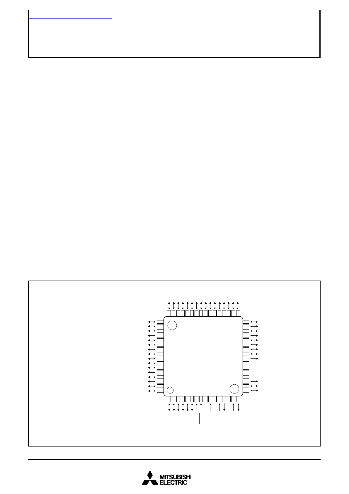
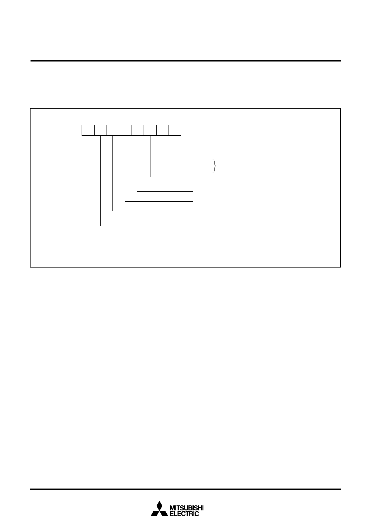
PIN CONFIGURATION (TOP VIEW)
P 40/ EXD R E Q / RXD
P 4
Fig. 1 Pin configuration of 38K0 group
3
2
1
6
5
7
5
P
24
S
S
V
C
N
5
P
14
T
R
E S E
5
P
03
E
C
C
V
4
5
P
93
1
01
F
R
V
E
1
/ EXD A C K / TXD
2
/ EXT C / S
P 4
P43/EXA1/S
P 33/ EXI N T
4
/ EXC S
P 3
5/EX
P3
P3
6/EX
7
/ EXA 0
P 3
P10/DQ0/AN
P1
1
/DQ1/AN
P 0
P 0
P 3
P 3
P 3
WR
C L K
RDY
RD
4
5
0
0
P
P
4
84
74
6
49
7
50
51
52
53
54
0
55
1
2
0
1
M 3 8 K 0 7 M 4 - X X X F P / H P
56
57
58
59
60
61
62
63
64
123456789
2
3
N
N
/
/
3
2
Q
Q
/
/
2
3
1
1
P
P
D
D
A
A
0
0
0
0
0
P
P
P
P
4
64
54
34
4
M 3 8 K 0 9 F 8 F P / H P
4
5
6
7
N
N
N
N
/
/
/
/
4
5
6
7
Q
Q
Q
Q
/
/
/
/
4
5
6
7
1
1
1
1
P
P
P
P
D
D
D
D
A
A
A
A
Package type : 64P6U-A/64P6Q-A
3
5
P
83
11
S
S
V
1
T
/
2
5
I N
P
73
21
N
I
X
/
1
5
C N T
I N
P
63
31
T
O
X
U
0
T
/
0
5
P
53
41
C
C
V
N
7
2
P
43
5
2
S
S
V
C
6
2
P
3
P 2
32
31
30
29
28
27
26
25
24
23
22
21
20
19
18
17
6
1
)
0
D
(
0
6
P
L E
5
P 2
4
P 2
3
P 2
2
P 2
1
P 2
0
D 0 D 0 +
T r O N
USBV
REF
DV
CC
P V
C C
P V
S S
3
( L E D3)
P 6
P 6
2
( L E D2)
P 61( L E D1)
1
Page 2
MITSUBISHI MICROCOMPUTERS
C
N T
R
0
V
S
S
E
S
E
T
C
C
I
N
W
a
t
c
h
d
o
g
t
i
m
e
r
i
m
e
r
X
(
8
)
T
i m e r 1 ( 8
)
i
m
e
r
2
(
8
)
O
U
T
C
l o c k
g
e n e r a t i n g
c
i r c u i
t
R
A
M
a t a b u
s
C
P
U
R
A
M
I
/
F
O
M
N
V
S
S
C
N
V
S
S
2
V
C
C
V
S
S
P
5 ( 8
)
N
T
1
N
T
0
5678901
2
6
(
4
)
678
9
4
(
4
)
I
/
O
E
X T B U S ( 8
)
P
3 ( 8
)
123
4
5
5
5
6
5
7
5
8
5
9
6
0
6
1
6
2
0
+
U
S
B
D
0
-
T
r O
N
S
B
V
R
E
F
V
C
C
2
2
3
2
4
2
6
5
P
0 ( 8
)
4
3
4
4
4
5
4
6
4
7
4
8
4
9
5
0
V
R
E
F
P
1 ( 8
)
0
-
b
i
t
A
-
D
o
n
v
e
r
t
e
r
(
8
)
0
6
3
6
4
12456
2
0
1
1
2
3
1
1
1
4
8
7
5
P
2 ( 8
)
789
01234
V
C
C
E
9
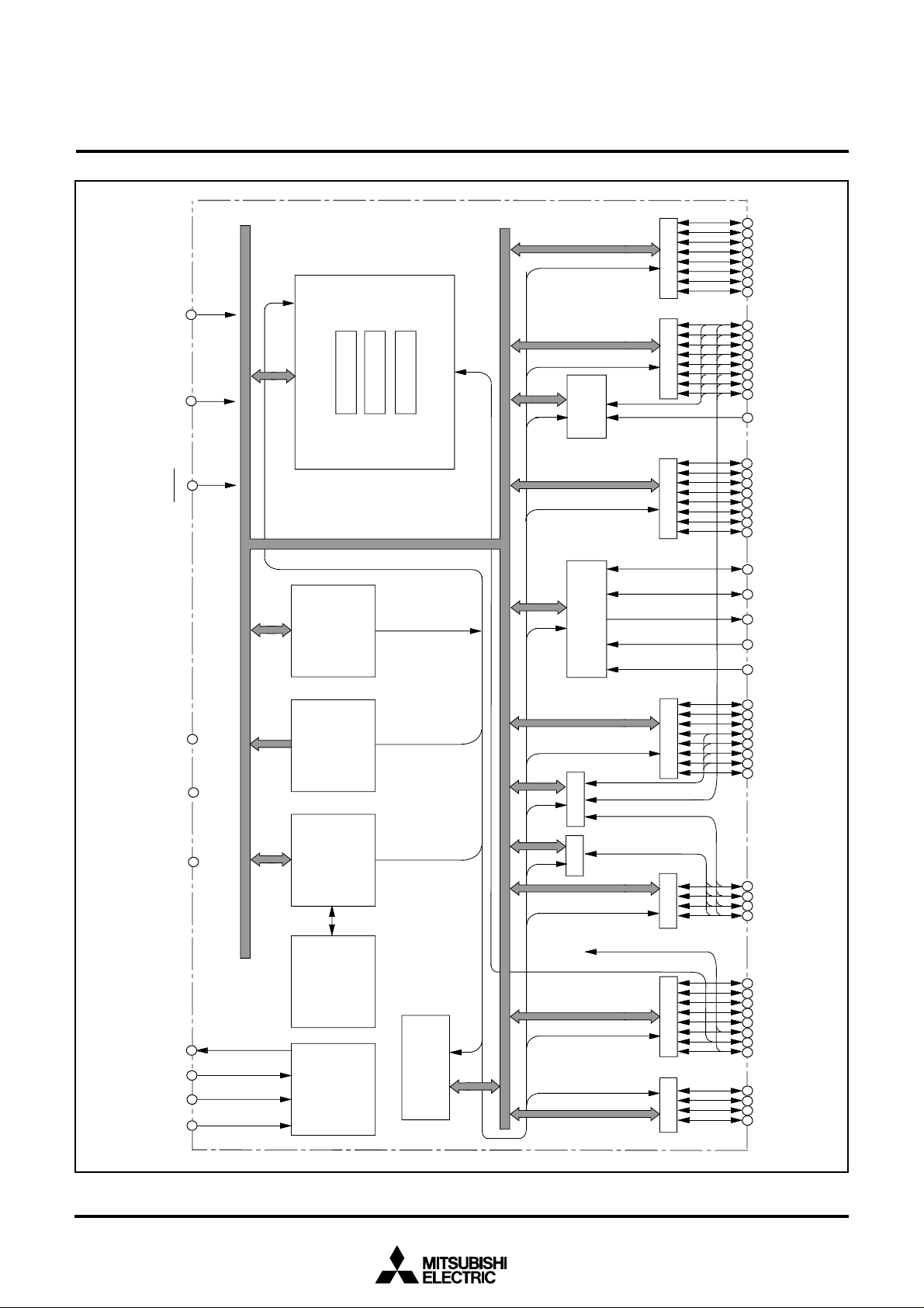
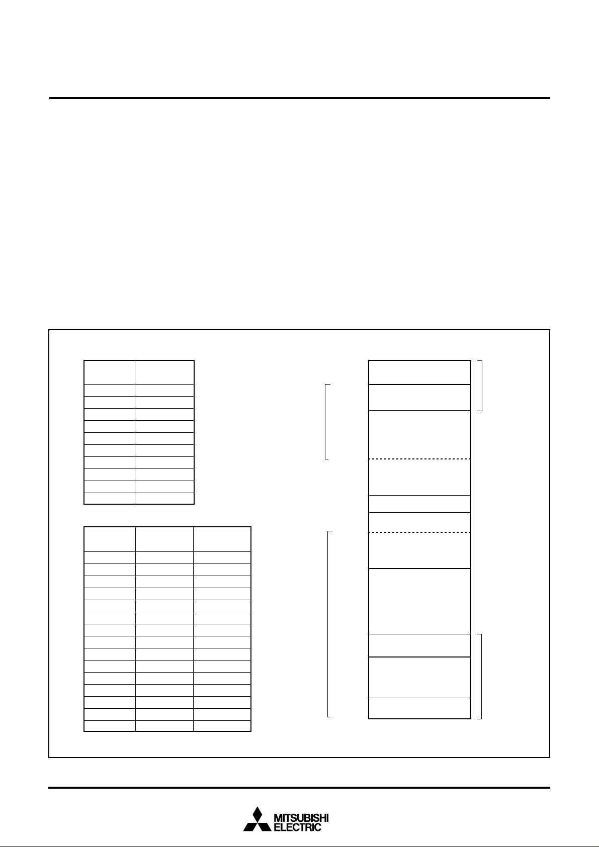
38K0 Group
SINGLE-CHIP 8-BIT CMOS MICROCOMPUTER
FUNCTIONAL BLOCK DIAGRAM (Package : 64P6U-A/64P6Q-A)
Fig. 2 Functional block diagram
2
Page 3
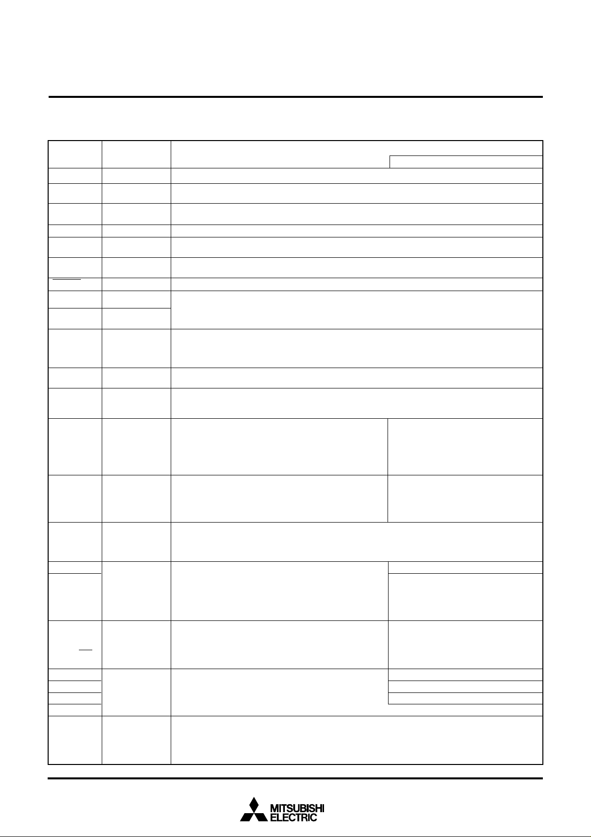
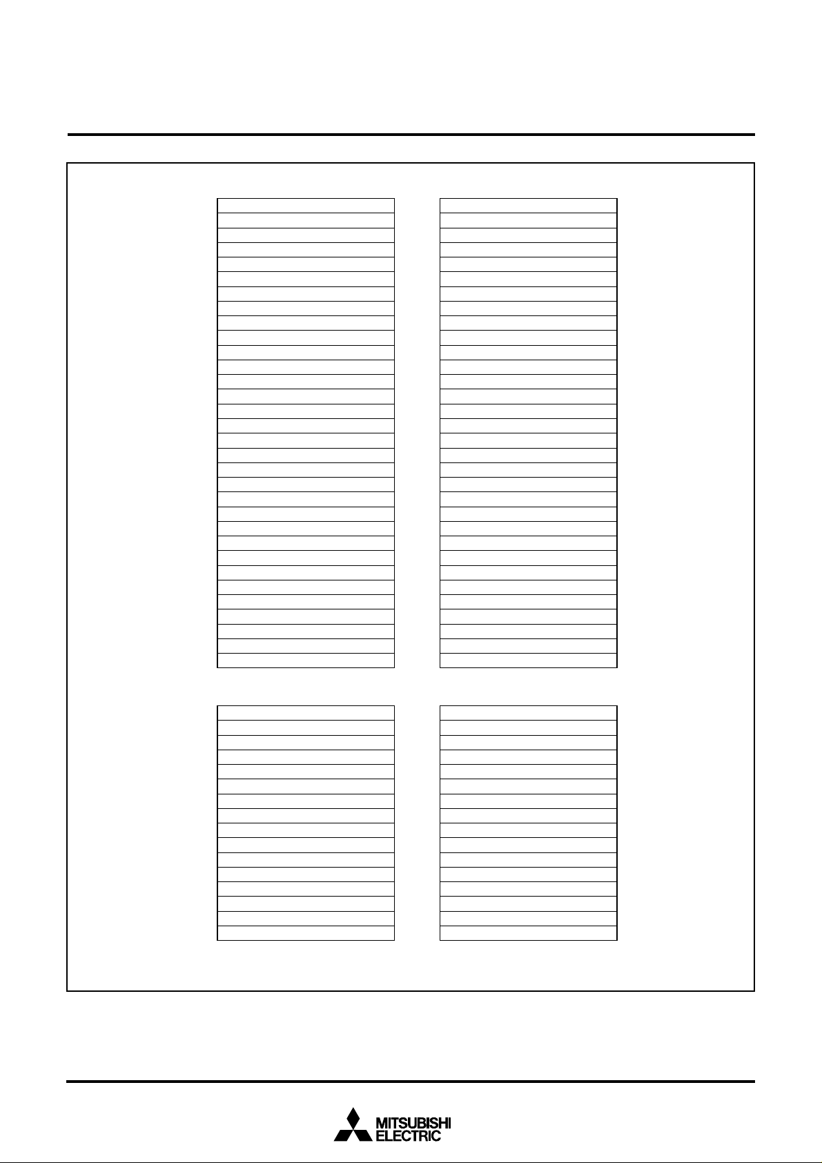
PIN DESCRIPTION
Table 1. Pin description
MITSUBISHI MICROCOMPUTERS
38K0 Group
SINGLE-CHIP 8-BIT CMOS MICROCOMPUTER
Pin
VCC, VSS
VCCE
CNVSS
CNVSS2
VREF
DVCC
PVCC, PVSS
RESET
XIN
XOUT
USBVREF
TrON
D0+, D0-
P00–P07
P10/DQ0/AN0–
P17/DQ7/AN
P20–P27
P30–P32
P33/ExINT
P34/ExCS
P35/ExWR
P36/ExRD
P37/ExA0
P40/ExDREQ/RxD
P41/ExDACK/TxD
P42/ExTC/S
P43/ExA1/S
P50/INT0
P51/CNTR0
P52/INT1
P53–P57
P60–P63
Power source
Analog power
source
CNVSS
CNVSS2
Analog reference
voltage input
Analog power
source
Reset input
Clock input
Clock output
USB reference
power source
USB reference
voltage output
USB upstream
I/O
I/O port P0
I/O port P1
7
I/O port P2
I/O port P3
I/O port P4
CLK
RDY
I/O port P5
I/O port P6
Name
Function
• Apply voltage of 3.0 V – 5.25 V to VCC, and 0 V to VSS.
• Power source pin for ports P1, P3, P4 and analog circuit. Connect this pin to VCC.
• This pin controls the operation mode of the chip. Connect this pin to VSS. In the flash memory
mode, this pin becoems VPP power source input pin.
• This pin controls the operation mode of the chip. Connect this pin to VSS.
• Reference voltage input pin for A-D converter.
• Power source pin for analog circuit.
• Connect the DVCC and PVCC pins to VCC, and the PVSS pin to VSS.
• Reset input pin for active “L”
• Input and output pins for the main clock generating circuit.
• Connect a ceramic resonator or a quartz-crystal oscillator between the XIN and XOUT pins to set
the oscillation frequency.
•If an external clock is used, connect the clock source to the XIN pin and leave the XOUT pin open.
• Power source pin for USB port circuit.
In Vcc = 4.00 to 5.25 V use the built-in USB reference voltage circuit. In Vcc = 3.00 to 4.00 V apply
3.3 V power supply from the external because use of the built-in USB reference voltage circuit is
prohibited in this voltage range. In Vcc = 3.00 to 3.60 V connect this pin to VCC.
• Output pin to pull-up D0+ by 1.5 kΩ external resistor.
• USB upstream I/O port
• USB input level
• USB output level output structure
• 8-bit I/O port
• I/O direction register allows each pin to be individually
programmed as either input or output.
• CMOS compatible input level
• CMOS 3-state output structure
• Pull-up control is enabled.
• 8-bit I/O port
• I/O direction register allows each pin to be individually
programmed as either input or output.
• CMOS compatible input level
• CMOS 3-state output structure
• 8-bit I/O port
• I/O direction register allows each pin to be individually programmed as either input or output.
• CMOS compatible input level
• CMOS 3-state output structure
• 8-bit I/O port
• I/O direction register allows each pin to be individually
programmed as either input or output.
• CMOS compatible input level
• CMOS 3-state output structure
• 4-bit I/O port
• I/O direction register allows each pin to be individually
programmed as either input or output.
• CMOS compatible input level
• CMOS 3-state output structure
• 8-bit I/O port
• I/O direction register allows each pin to be individually
programmed as either input or output.
• CMOS compatible input level
• CMOS 3-state output structure
• 4-bit I/O port
• I/O direction register allows each pin to be individually programmed as either input or output.
• CMOS compatible input level
• CMOS 3-state output structure
• Output large current for LED drive is enabled.
Function except a port function
• Key input pins (key-on wake up interrupt)
• A-D converter input pins
• External bus interface function pins
• External bus interface function pins
• Serial I/O function pins
• External bus interface function pins
• Interrupt input pin
• Timer X funciton pin
• Interrupt input pin
3
Page 4
PART NUMBERING
MITSUBISHI MICROCOMPUTERS
38K0 Group
SINGLE-CHIP 8-BIT CMOS MICROCOMPUTER
P r o d u c t
M 3 8 K0 7 M 4 - X X X FP
P a c k a g e t y p e
F P : 6 4 P 6 U - A p a c k a g e
H P : 6 4 P 6 Q - A p a c k a g e
R O M n u m b e r
O m i t t e d i n t h e f l a s h m e m o r y v e r s i o n .
– : Standard
Omitted in the flash memory version.
R O M / P R O M s i z e
1 : 4 0 9 6 b y t e s
2 : 8 1 9 2 b y t e s
3 : 1 2 2 8 8 b y t e s
4 : 1 6 3 8 4 b y t e s
5 : 2 0 4 8 0 b y t e s
6 : 2 4 5 7 6 b y t e s
7 : 2 8 6 7 2 b y t e s
8 : 3 2 7 6 8 b y t e s
T h e f i r s t 1 2 8 b y t e s a n d t h e l a s t 2 b y t e s o f R O M
a r e r e s e r v e d a r e a s ; t h e y c a n n o t b e u s e d a s a
u s e r ’ s R O M a r e a .
H o w e v e r , t h e y c a n b e p r o g r a m m e d o r e r a s e d i n
t h e f l a s h m e m o r y v e r s i o n , s o t h a t u s e r s c a n
u s e t h e m .
9 : 3 6 8 6 4 b y t e s
A : 4 0 9 6 0 b y t e s
B : 4 5 0 5 6 b y t e s
C : 4 9 1 5 2 b y t e s
D : 5 3 2 4 8 b y t e s
E : 5 7 3 4 4 b y t e s
F : 6 1 4 4 0 b y t e s
Fig. 3 Part numbering
Memory type
M : Mask ROM version
F : Flash memory version
R A M s i z e
0 : 1 9 2 b y t e s
1 : 2 5 6 b y t e s
2 : 3 8 4 b y t e s
3 : 5 1 2 b y t e s
4 : 6 4 0 b y t e s
5 : 7 6 8 b y t e s
6 : 8 9 6 b y t e s
7 : 1 0 2 4 b y t e s
8 : 1 5 3 6 b y t e s
9 : 2 0 4 8 b y t e s
4
Page 5
MITSUBISHI MICROCOMPUTERS
38K0 Group
SINGLE-CHIP 8-BIT CMOS MICROCOMPUTER
GROUP EXPANSION
Mitsubishi plans to expand the 38K0 group as follows.
Memory Type
Support for mask ROM and flash memory versions.
Memory Size
Flash memory size .......................................................... 32 Kbytes
Mask ROM size ............................................................... 16 Kbytes
RAM size .......................................................... 1024 to 2048 bytes
Memory Expansion Plan
: U n d e r d e v e l o p m e n t
R O M s i z e
( b y t e s )
6 0 K
3 2 K
Packages
64P6U-A .................................. 0.8 mm-pitch plastic molded LQFP
64P6Q-A .................................. 0.5 mm-pitch plastic molded LQFP
100D0M ...........................0.65 mm-pitch metal seal PIGGY BACK
M 3 8 K 0 9 F 8
1 6 K
8 K
P r o d u c t s u n d e r d e v e l o p m e n t o r p l a n n i n g : t h e d e v e l o p m e n t s c h e d u l e a n d s p e c i f i c a t i o n m a y b e r e v i s e d
w i t h o u t n o t i c e . T h e d e v e l o p m e n t o f p l a n n i n g p r o d u c t s m a y b e s t o p p e d .
Fig. 4 Memory expansion plan
Currently products are listed below.
Table 2. List of products
Product
M38K07M4-XXXFP
M38K07M4-XXXHP
M38K09F8FP
M38K09F8HP
M38K09RFS
ROM size (bytes)
ROM size for User in ( )
16384
(16254)
32768
(32638)
2 5 65
—
1
21
RAM size (bytes)
1024
2048
2048
M 3 8 K 0 7 M 4
R A M s i z e ( b y t e s )
Package
64P6U-A
64P6Q-A
64P6U-A
64P6Q-A
100D0M
, 0 2
42
Mask ROM version
Flash memory version
Emulator MCU (for program evaluation)
, 0 4
8
Remarks
As of February 2002
5
Page 6
MITSUBISHI MICROCOMPUTERS
38K0 Group
SINGLE-CHIP 8-BIT CMOS MICROCOMPUTER
FUNCTIONAL DESCRIPTION
CENTRAL PROCESSING UNIT (CPU)
The 38K0 group uses the standard 740 family instruction set. Refer to the table of 740 family addressing modes and machine
instructions or the 740 Family Software Manual for details on the
instruction set.
Machine-resident 740 family instructions are as follows:
The FST and SLW instruction cannot be used.
The STP, WIT, MUL, and DIV instruction can be used.
The CPU has the 6 registers. The register structure is shown in
Figure 5.
[Accumulator (A)]
The accumulator is an 8-bit register. Data operations such as data
transfer, etc., are executed mainly through the accumulator.
[Index Register X (X)]
The index register X is an 8-bit register. In the index addressing
modes, the value of the OPERAND is added to the contents of
register X and specifies the real address.
[Index Register Y (Y)]
The index register Y is an 8-bit register. In partial instruction, the
value of the OPERAND is added to the contents of register Y and
specifies the real address.
[Stack Pointer (S)]
The stack pointer is an 8-bit register used during subroutine calls
and interrupts. This register indicates start address of stored area
(stack) for storing registers during subroutine calls and interrupts.
The low-order 8 bits of the stack address are determined by the
contents of the stack pointer. The high-order 8 bits of the stack
address are determined by the stack page selection bit. If the
stack page selection bit is “0” , the high-order 8 bits becomes
“0016”. If the stack page selection bit is “1”, the high-order 8 bits
becomes “0116”.
Figure 6 shows the store and the return movement into the stack.
If there are registers other than those described in Figure 5, the
users need to store them with the program.
[Program Counter (PC)]
The program counter is a 16-bit counter consisting of two 8-bit
registers PCH and PCL. It is used to indicate the address of the
next instruction to be executed.
b7
b0
A Accumulator
b7
b0
X Index register X
b7
b0
Y Index register Y
b7 b0
S Stack pointer
b7b15 b0
H
PC
L
Program counterPC
b7 b0
N V T B D I Z C Processor status register (PS)
Carry flag
Zero flag
Interrupt disable flag
Decimal mode flag
Break flag
Index X mode flag
Overflow flag
Negative flag
Fig. 5 740 Family CPU register structure
6
Page 7
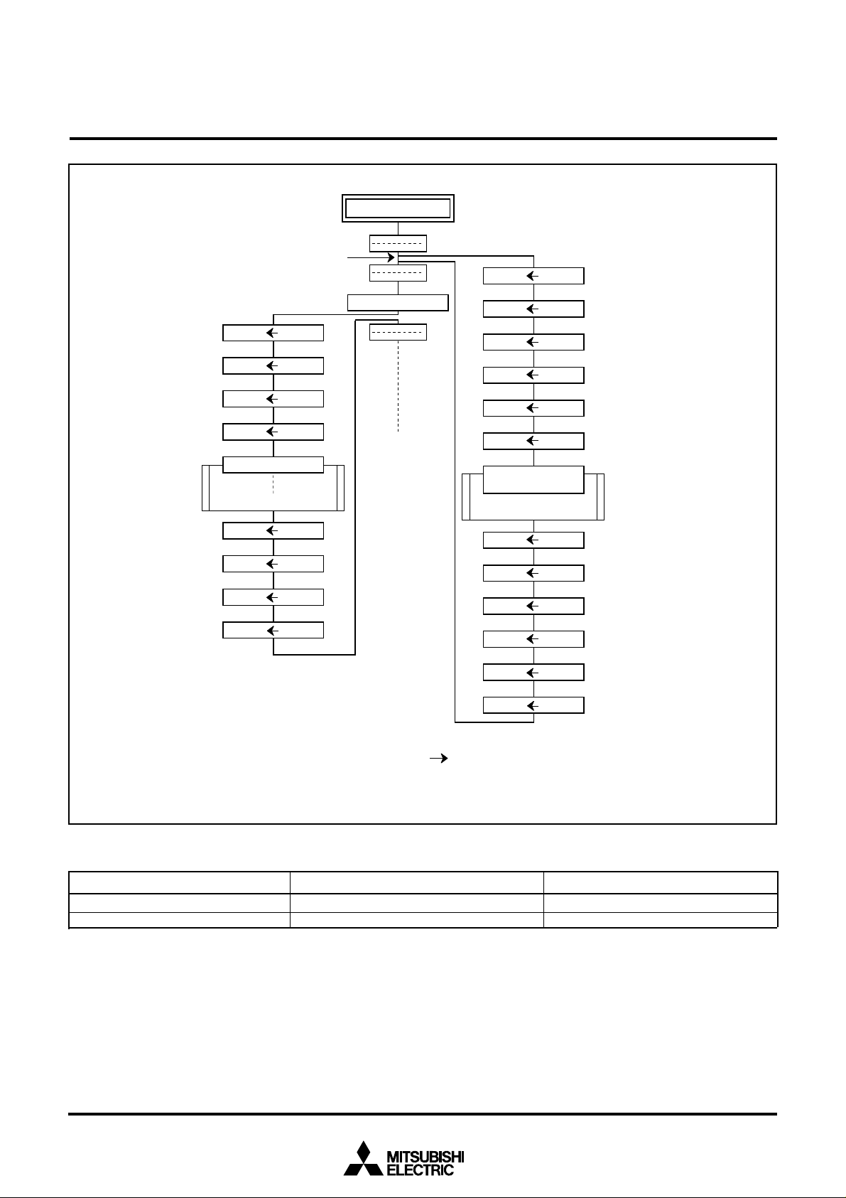
e
I n t e r r u p t r e q u e s t
( N o t e )
O n - g o i n g R o u t i n
MITSUBISHI MICROCOMPUTERS
38K0 Group
SINGLE-CHIP 8-BIT CMOS MICROCOMPUTER
M (S) (PCH)
P u s h r e t u r n a d d r e s s
o n s t a c k
P O P re t u r n
a d d r e s s f r o m s t a c k
M ( S )( P CH)
S ) –
( S )
(
1
M ( S )( P CL)
(S) (S)– 1
S u b r o u t i n e
E x e c u t e R T S
S ) +
( S )
(
1
(PCL)M (S)
(S) (S) + 1
( P CH)M ( S )
E x e c u t e J S R
(S) (S) – 1
M ( S )( P CL)
S ) –
( S )
(
1
M (S) (PS)
(S) (S) – 1
I n t e r r u p t
S e r v i c e R o u t i n e
Execute RTI
(S) (S) + 1
( P S )M ( S )
(S) (S) + 1
(PCL)M (S)
(S) (S) + 1
(PCH)M (S)
P u s h r e t u r n a d d r e s s
o n s t a c k
P u s h c o n t e n t s o f p r o c e s s o r
s t a t u s r e g i s t e r o n s t a c k
I Flag is set from “0” to “1”
Fetch the jump vector
POP contents of
processor status
register from stack
P O P r e t u r n
a d d r e s s
f r o m s t a c k
N o t e: C o n d i t i o n f o r a c c e p t a n c e o f a n i n t e r r u p t I n t e r r u p t e n a b l e f l a g i s “ 1 ”
Fig. 6 Register push and pop at interrupt generation and subroutine call
Table 3 Push and pop instructions of accumulator or processor status register
Push instruction to stack
Accumulator
Processor status register
PHA
PHP
I n t e r r u p t d i s a b l e f l a g i s “ 0 ”
Pop instruction from stack
PLA
PLP
7
Page 8
MITSUBISHI MICROCOMPUTERS
38K0 Group
SINGLE-CHIP 8-BIT CMOS MICROCOMPUTER
[Processor status register (PS)]
The processor status register is an 8-bit register consisting of 5
flags which indicate the status of the processor after an arithmetic
operation and 3 flags which decide MCU operation. Branch operations can be performed by testing the Carry (C) flag , Zero (Z) flag,
Overflow (V) flag, or the Negative (N) flag. In decimal mode, the Z,
V, N flags are not valid.
•Bit 0: Carry flag (C)
The C flag contains a carry or borrow generated by the arithmetic
logic unit (ALU) immediately after an arithmetic operation. It can
also be changed by a shift or rotate instruction.
•Bit 1: Zero flag (Z)
The Z flag is set if the result of an immediate arithmetic operation
or a data transfer is “0”, and cleared if the result is anything other
than “0”.
•Bit 2: Interrupt disable flag (I)
The I flag disables all interrupts except for the interrupt
generated by the BRK instruction.
Interrupts are disabled when the I flag is “1”.
•Bit 3: Decimal mode flag (D)
The D flag determines whether additions and subtractions are
executed in binary or decimal. Binary arithmetic is executed when
this flag is “0”; decimal arithmetic is executed when it is “1”.
Decimal correction is automatic in decimal mode. Only the ADC
•Bit 4: Break flag (B)
The B flag is used to indicate that the current interrupt was
generated by the BRK instruction. The BRK flag in the processor
status register is always “0”. When the BRK instruction is used to
generate an interrupt, the processor status register is pushed
onto the stack with the break flag set to “1”.
•Bit 5: Index X mode flag (T)
When the T flag is “0”, arithmetic operations are performed
between accumulator and memory. When the T flag is “1”, direct
arithmetic operations and direct data transfers are enabled
between memory locations.
•Bit 6: Overflow flag (V)
The V flag is used during the addition or subtraction of one byte
of signed data. It is set if the result exceeds +127 to -128. When
the BIT instruction is executed, bit 6 of the memory location
operated on by the BIT instruction is stored in the overflow flag.
•Bit 7: Negative flag (N)
The N flag is set if the result of an arithmetic operation or data
transfer is negative. When the BIT instruction is executed, bit 7 of
the memory location operated on by the BIT instruction is stored
in the negative flag.
Table 4 Set and clear instructions of each bit of processor status register
Set instruction
Clear instruction
C flag
SEC
CLC
Z flag
–
–
I flag
SEI
CLI
D flag
SED
CLD
B flag
–
–
T flag
SET
CLT
V flag
–
CLV
N flag
–
–
8
Page 9
[CPU Mode Register (CPUM)] 003B16
P
CPU
( C P U M
B
)
b
b
The CPU mode register contains the stack page selection bit and
the internal system clock selection bit.
The CPU mode register is allocated at address 003B16.
MITSUBISHI MICROCOMPUTERS
38K0 Group
SINGLE-CHIP 8-BIT CMOS MICROCOMPUTER
7
Fig. 7 Structure of CPU mode register
0
10
mode register
: a d d r e s s 0 0 3
rocessor mode bits
b1 b0
0 0 : Single-chip mode
01 :
1 0 : Not availab le
11 :
Stack page selection bit
0 : 0 page
1 : 1 page
Not used (returns “1” when read)
(Do not write “0” to this bit)
Not used (returns “0” when read)
(Do not write “1” to this bit)
System clock selection bit
0 : Main clock (X
SYN
1 : f
System clock division ratio selection bits
b7 b6
00 :
01 :
10 :
11 :
1 6
IN
)
φ
= f(system clock)/8 (8-divide mode)
φ
= f(system clock)/4 (4-divide mode)
φ
= f(system clock)/2 (2-divide mode)
φ
= f(system clock) (Through mode)
9
Page 10
MITSUBISHI MICROCOMPUTERS
FF
RAM
R A M
A d d
6
2
8
4
0
6
2
8
4
0
6
2
8
4
0
F
F
ROM
ROM si
A d d
A d d
FF
FFDC
F F F E
FFFF
XXXX
YYYY
ZZZZ
RAM
R O M
S F R
N
d
I
a
R
ROM
Z
S
R
FFF
S F R
38K0 Group
SINGLE-CHIP 8-BIT CMOS MICROCOMPUTER
MEMORY
Special Function Register (SFR) Area
The Special Function Register area in the zero page contains control registers such as I/O ports and timers.
RAM
RAM is used for data storage and for stack area of subroutine
calls and interrupts.
ROM
The first 128 bytes and the last 2 bytes of ROM are reserved for
device testing and the rest is user area for storing programs. In
the flash memory version, program and erase can be performed in
the reserved area.
area
s i z
( b y t e s )
192
256
384
512
640
768
896
1024
1536
2048
area
(bytes)
4 0 9
8 1 9
1 2 2 8
1 6 3 8
2 0 4 8
2 4 5 7
2 8 6 7
3 2 7 6
3 6 8 6
4 0 9 6
4 5 0 5
4 9 1 5
5 3 2 4
5 7 3 4
6 1 4 4
Fig. 8 Memory map diagram
r e s s
e
r e s
ze
X X X X
00
013F
01BF
023F
02BF
033F
03BF
043F
063F
083F
Y Y Y Y
0 0
E 0 0 0
D 0 0 0
C 0 0 0
B 0 0 0
A 0 0 0
9 0 0 0
8 0 0 0
7 0 0 0
6 0 0 0
5 0 0 0
4 0 0 0
3 0 0 0
2 0 0 0
1 0 0 0
1 6
16
16
16
16
16
16
16
16
16
16
r e s
s
1 6
1 6
0
1 6
1 6
1 6
1 6
1 6
1 6
1 6
1 6
1 6
1 6
1 6
1 6
1 6
1 6
Z Z Z Z
0 8
E 0 8 0
D 0 8 0
C 0 8 0
B 0 8 0
A 0 8 0
9 0 8 0
8 0 8 0
7 0 8 0
6 0 8 0
5 0 8 0
4 0 8 0
3 0 8 0
2 0 8 0
1 0 8 0
s
1 6
1 6
0
1 6
1 6
1 6
1 6
1 6
1 6
1 6
1 6
1 6
1 6
1 6
1 6
1 6
1 6
Interrupt Vector Area
The interrupt vector area contains reset and interrupt vectors.
Zero Page
The 256 bytes from addresses 000016 to 00FF16 are called the
zero page area. The internal RAM and the special function registers (SFR) are allocated to this area.
The zero page addressing mode can be used to specify memory
and register addresses in the zero page area. Access to this area
with only 2 bytes is possible in the zero page addressing mode.
Special Page
The 256 bytes from addresses FF0016 to FFFF16 are called the
special page area. The special page addressing mode can be
used to specify memory addresses in the special page area. Access to this area with only 2 bytes is possible in the special page
addressing mode.
0000
0040
0100
0FE0
0
16
16
16
16
16
16
16
16
00
16
16
1 6
e s e r v e d R O M a r e
16
eserved
n t e r r u p t v e c t o r a r e
a r e
ot use
a r e
(128 by tes)
a
a
area
e r o p a g
e
p e c i a l p a g
e
a
10
Page 11
MITSUBISHI MICROCOMPUTERS
A
B
C
D
E
F
A
B
C
D
E
F
A
B
C
D
E
F
A
B
C
D
E
F
P
)
P
)
P
)
P
)
P
)
P
)
P
)
P
D)
P
)
P
)
P
)
P
)
Serial I/O
(SIOSTS)
I
(ICON2)
T
CPU
(CPUM)
I
(IREQ1)
I
(IREQ2)
I
(ICON1)
P
(PRE12)
Ti
)
P
(PREX)
Ti
(TX)
Ti
)
Ti
(TM)
A-D
(ADCON)
A-D
(ADL)
P
)
P
D)
R
)
R
( N
)
U S B
l
i
)
U S B
)
USB add
(USBA0)
USB add
(USBA1)
E
)
E
)
Endpoi
(EPXXREG2)
E
)
E
)
E
)
Endpoi
(EPXXREG6)
E
)
R
( N
)
R
( N
)
R
( N
)
R
( N
)
R
( N
)
R
( N
)
R
( N
)
R
)
F
)
F
)
U S B
E XB
R
)
EXB ind
(EXBINDEX)
E X B
)
E X B
)
A-D
(ADH)
R
)
F E
F E
F E
F E
F E
F E A
Flash
(FMCR)
P L L
( P L L C O N )
P
(PULL5)
Endpoi
(EPXXREG8)
Endpoi
(EPXXREG9)
S
)
UART
(UARTCON)
B
)
P
l
i
)
R
( N
)
F E B
F E C
F E D
FEE
F E F
F F
F F
F F
F F
F F
F F A
FFB
F F C
F F D
FFE
F F F
R
)
R
( N
)
R
( N
)
R
( N
)
R
)
R
( N
)
R
)
R
( N
)
R
( N
)
R
( N
)
R
)
R
( N
)
R
( N
)
R
( N
)
R
( N
)
M I S R G
R
( N
)
R
( N
)
R
)
R
( N
)
R
( N
)
N
38K0 Group
SINGLE-CHIP 8-BIT CMOS MICROCOMPUTER
o r t P 0 ( P 0
0 0 0 0
1 6
o r t P 0 d i r e c t i o n r e g i s t e r ( P 0 D
0 0 0 1
1 6
o r t P 1 ( P 1
0 0 0 2
1 6
o r t P 1 d i r e c t i o n r e g i s t e r ( P 1 D
0 0 0 3
1 6
o r t P 2 ( P 2
0 0 0 4
1 6
o r t P 2 d i r e c t i o n r e g i s t e r ( P 2 D
0 0 0 5
1 6
o r t P 3 ( P 3
0 0 0 6
1 6
0 0 0 7
1 6
ort P3 direction register (P3
o r t P 4 ( P 4
0 0 0 8
1 6
0 0 0 9
1 6
0 0 0
0 0 0
0 0 0
0 0 0
0 0 0
0 0 0
0 0 1 0
0 0 1 1
0012
0013
0 0 1 4
0 0 1 5
0 0 1 6
0017
0018
0 0 1 9
0 0 1
001
0 0 1
001
001
0 0 1
ort P4 direction register (P4
o r t P 5 ( P 5
1 6
o r t P 5 d i r e c t i o n r e g i s t e r ( P 5 D
1 6
1 6
ort P6 (P6
o r t P 6 d i r e c t i o n r e g i s t e r ( P 6 D
1 6
1 6
eserved (Note
e s e r v e d
o t e
1 6
1 6
1 6
16
16
1 6
1 6
1 6
16
16
1 6
1 6
16
1 6
16
16
1 6
c o n t r o
s t e r ( U S B C O N
a d d r e s s e n a b l e r e g i s t e r ( U S B A E
ress 0 register
ress 1 register
r a m e n u m b e r r e g i s t e r L o w ( F N U M L
r a m e n u m b e r r e g i s t e r H i g h ( F N U M H
U S B i n t e r r u p t s o u r c e e n a b l e r e g i s t e r
i n t e r r u p t s o u r c e r e g i s t e
n d p o i n t i n d e x r e g i s t e r ( U S B I N D E X
n d p o i n t f i e l d r e g i s t e r 1 ( E P X X R E G 1
nt field register 2
n d p o i n t f i e l d r e g i s t e r 3 ( E P X X R E G 3
n d p o i n t f i e l d r e g i s t e r 4 ( E P X X R E G 4
n d p o i n t f i e l d r e g i s t e r 5 ( E P X X R E G 5
nt field register 6
n d p o i n t f i e l d r e g i s t e r 7 ( E P X X R E G 7
r e g
( U S B I C O N )
( U S B I R E Q )
r
0020
16
0021
0022
0023
0024
0025
0026
0027
0028
0029
0 0 2
0 0 2
002
002
0 0 2
0 0 2
0030
0031
0032
0033
0034
0035
0036
0037
0038
0039
0 0 3
003
003
003
003
0 0 3
rescaler 12
16
mer 1 (T1
16
mer 2 (T2
16
mer X mode register
16
rescaler X
16
mer X
16
ransmit/Receive buffer register
16
16
16
1 6
1 6
16
16
1 6
1 6
16
16
16
16
16
16
16
16
16
16
1 6
16
16
16
16
1 6
status register
e s e r v e d
o t e
e s e r v e d
o t e
e s e r v e d
o t e
e s e r v e d
o t e
e s e r v e d
o t e
e s e r v e d
o t e
e s e r v e d
o t e
eserved (Note
E X B i n t e r r u p t s o u r c e e n a b l e r e g i s t e r
i n t e r r u p t s o u r c e r e g i s t e
eserved (Note
ex register
f i e l d r e g i s t e r 1 ( E X B R E G 1
f i e l d r e g i s t e r 2 ( E X B R E G 2
control register
conversion register Low
conversion register High
Watchdo g timer control register (WDTCON)
eserved (Note
mode register
nterrupt request register 1
nterrupt request register 2
nterrupt co ntrol register 1
nterrupt co ntrol register 2
(TB/RB)
( E X B I C O N )
( E X B I R E Q )
r
e r i a l I / O c o n t r o l r e g i s t e r ( S I O C O N
0
1 6
0
0
1 6
0
0FE3
0FE4
0
0FE6
0
0FE8
0FE9
0
0
0
0
0
0
1
2
1 6
5
16
7
16
1 6
16
a u d r a t e g e n e r a t o r ( B R G
1 6
16
eserved (Note
e s e r v e d
o t e
16
e s e r v e d
o t e
e s e r v e d
o t e
1 6
eserved (Note
e s e r v e d
o t e
16
eserved (Note
e s e r v e d
o t e
1 6
e s e r v e d
o t e
1 6
1 6
e s e r v e d
o t e
eserved (Note
1 6
control register
nt field register 8
nt field register 9
o t e: D o n o t w r i t e a n y d a t a t o t h e s e a d d r e s s e s , b e c a u s e t h e s e a r e a s a r e r e s e r v e d
Fig. 9 Memory map of special function register (SFR)
o r t P 0 p u l l - u p c o n t r o
s t e r ( P U L L 0
0
1 6
0
e s e r v e d
o t e
0
1 6
1
0
1 6
2
0FF3
16
Interrupt edge selection regi s ter (INTEDGE)
e s e r v e d
o t e
0FF4
16
e s e r v e d
o t e
0
1 6
5
e s e r v e d
o t e
0FF6
16
e s e r v e d
o t e
0
1 6
7
c o n t r o l r e g i s t e r
0FF8
16
e s e r v e d
o t e
0FF9
16
e s e r v e d
o t e
0
1 6
0
16
0
1 6
e s e r v e d
o t e
0
1 6
0
16
e s e r v e d
o t e
0
1 6
ort P5 pull-up co ntrol register
eserved (Note
memory control register
r e g
.
11
Page 12
MITSUBISHI MICROCOMPUTERS
38K0 Group
SINGLE-CHIP 8-BIT CMOS MICROCOMPUTER
I/O PORTS
The I/O ports have direction registers which determine the input/
output direction of each individual pin. Each bit in a direction register corresponds to one pin, and each pin can be set to be input
port or output port.
When “0” is written to the bit corresponding to a pin, that pin becomes an input pin. When “1” is written to that bit, that pin becomes an output pin.
If data is read from a pin set to output, the value of the port output
latch is read, not the value of the pin itself. Pins set to input are
floating. If a pin set to input is written to, only the port output latch
is written to and the pin remains floating.
Table 5 I/O ports functions
Pin
P00–P07
P10–P17
P20–P27
P30–P32
P33/ExINT
P34/ExCS
P35/ExWR
P36/ExRD
P37/ExA0
P40/RxD/
ExDREQ
P41/TxD/
ExDACK
P42/SCLK/
ExTC
P43/SRDY/
ExA1
P50/INT0
P52/INT1
P51/CNTR0
P53–P57
P60–P63
Note: Make sure that the input level at each pin is either 0 V or VCC during execution of the STP instruction. When an input level is at an intermediate poten-
tial, a current will flow from VCC to VSS through the input-stage gate.
Name
Port P0
Port P1
Port P2
Port P3
Port P4
Port P5
Port P6
Input/Output
Input/output,
individual bits
I/O Format
CMOS compatible
input level
CMOS 3-state output
CMOS compatible
input level
CMOS 3-state output
(Power source is
VCCE)
CMOS compatible
input level
CMOS 3-state output
CMOS/TTL compatible input level
CMOS 3-state output
(Power source is
VccE)
CMOS compatible
input level
CMOS 3-state output
Non-Port Function
Key-on wake up
A-D conversion input
External bus interface
funciton I/O
External bus interface
funciton output
External bus interface
funciton input
Serial I/O input
External bus interface
funciton output
Serial I/O output
External bus interface
funciton input
Serial I/O I/O
External bus interface
funciton input
Serial I/O output
External bus interface
funciton input
External interrupt input
Timer X function I/O
Related SFRs
Port P0 pull-up control
register
A-D control register
EXB control register
EXB control register
EXB control register
Serial I/O control
register
EXB control register
Serial I/O control
register
EXB control register
Serial I/O control
register
EXB control register
Serial I/O control
register
EXB control register
Port P5 pull-up control
register
Interrupt edge selection
register
Timer X mode register
Diagram No.
(1)
(2)
(3)
(4)
(5)
(6)
(7)
(8)
(9)
(10)
(11)
(12)
(13)
(14)
12
Page 13
MITSUBISHI MICROCOMPUTERS
38K0 Group
SINGLE-CHIP 8-BIT CMOS MICROCOMPUTER
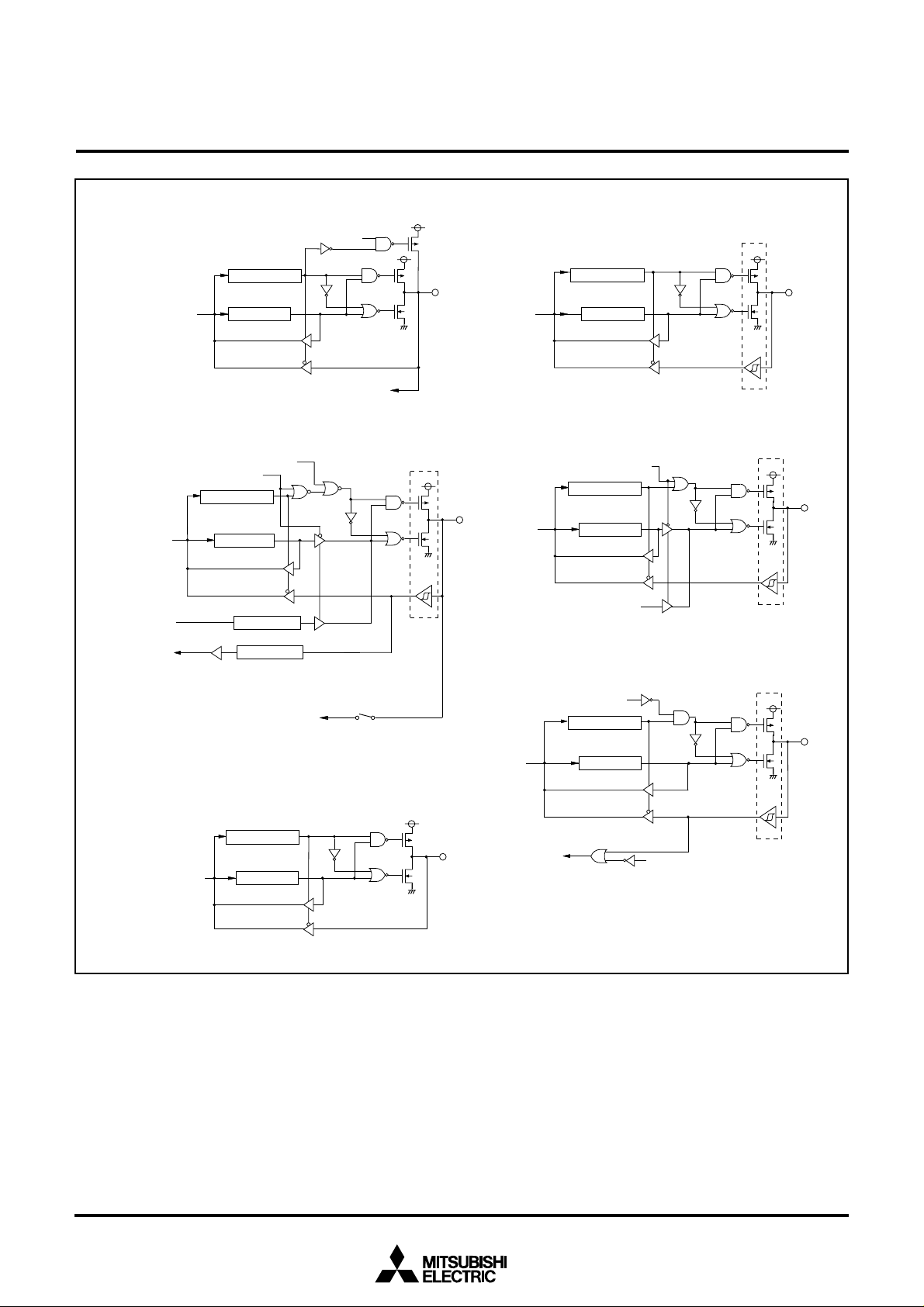
( 1 ) P o r t P 0
D a t a b u s
( 2 ) P o r t P 1
E x t e r n a l b u s i n t e r f a c e e n a b l e b i t
D i r e c t i o n r e g i s t e r
D a t a b u s
E X B d a t a o u t p u t
E X B d a t a i n p u t
P u l l - u p c o n t r o l b i t
D i r e c t i o n r e g i s t e r
P o r t l a t c h
K e y - o n w a k e - u p i n p u t
EXO E
P o r t l a t c h
O u t p u t b u f f e r
I n p u t b u f f e r
A - D c o n v e r s i o n i n p u t
VC
CE
A n a l o g i n p u t p i n s e l e c t i o n b i t
(4) Ports P30–P32
D i r e c t i o n r e g i s t e r
D a t a b u sP
o r t l a t c
h
( 5 ) P o r t P 33
E x t e r n a l b u s i n t e r f a c e e n a b l e b i t
D i r e c t i o n r e g i s t e r
D a t a b u s
P o r t l a t c h
EXI N T o u t p u t
( 6 ) P o r t s P 34, P 35, P 36, P 37
E x t e r n a l b u s i n t e r f a c e e n a b l e b i t
D i r e c t i o n r e g i s t e r
D a t a b u sP
o r t l a t c
h
C CE
V
VC
CE
VC
CE
( 3 ) P o r t P 2
D i r e c t i o n r e g i s t e r
D a t a b u s
P o r t l a t c h
Fig. 10 Port block diagram (1)
D ( P
0 ( P
R ( P
EXC S ( P 34)
E
XW
E
XR
36)
E
XA
37)
35)
E x t e r n a l b u s i n t e r f a c e e n a b l e b i t
13
Page 14
MITSUBISHI MICROCOMPUTERS
k
38K0 Group
SINGLE-CHIP 8-BIT CMOS MICROCOMPUTER
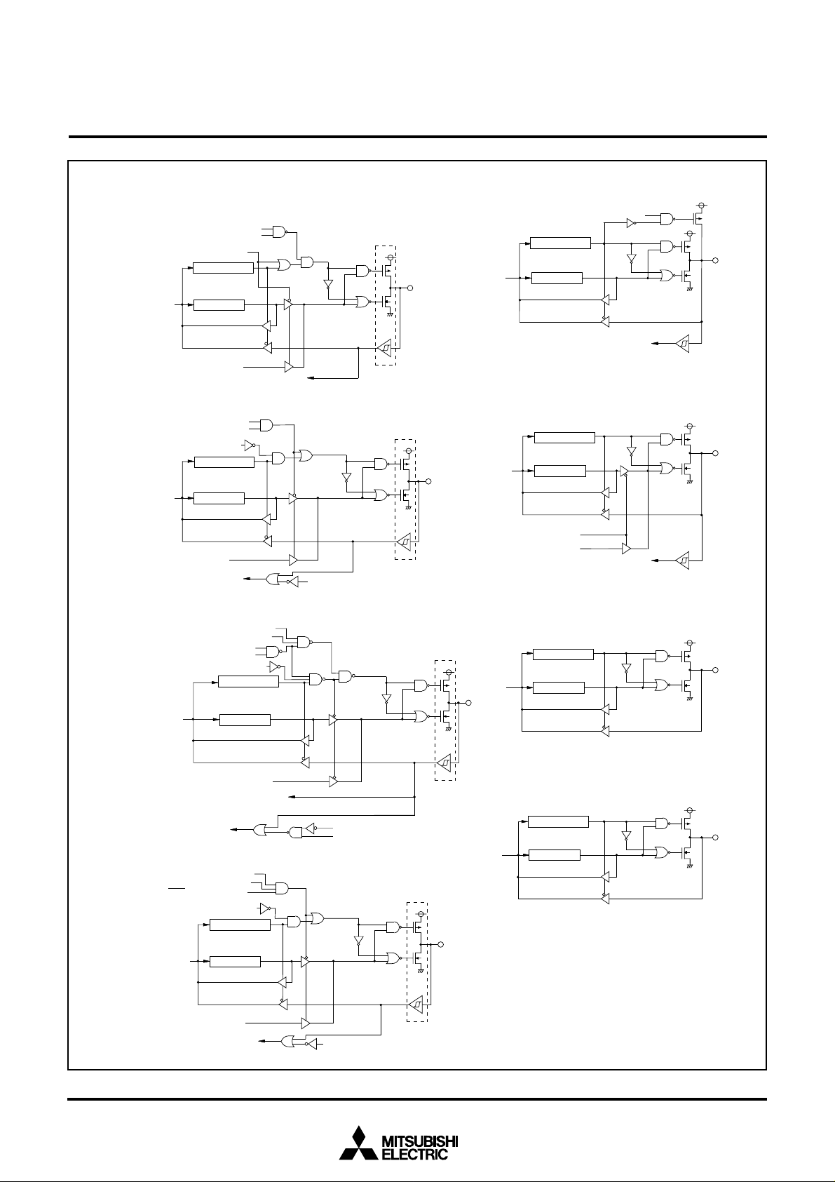
(7) Port P4
E x t e r n a l b u s i n t e r f a c e e n a b l e b i t
Data bus
(8) Port P4
External bus interface enable bit
D a t a b u s
0
S e r i a l I / O e n a b l e b i t
R e c e i v e e n a b l e b i t
D i r e c t i o n r e g i s t e r
P o r t l a t c h
E
X
D r e q o u t p u t
1
S e r i a l I / O e n a b l e b i t
Receive enable bit
Direction register
P o r t l a t c h
Serial I/O output
EXDac
S e r i a l I / O i n p u t
V
C C
E
V
C C
E
E x t e r n a l b u s i n t e r f a c e e n a b l e b i t
( 1 1 ) P o r t s P 5
D a t a b u s
( 1 2 ) P o r t P 5
Data bus
0 ,
P 5
2
Direction register
Port latch
I N T
0
( P 50) , I N T
1
D i r e c t i o n r e g i s t e r
Port latch
Pulse output mode
Timer output
Pull-up control bit
1
( P 52) i n t e r r u p t i n p u t
CNTR0 interrupt input
(9) Port P4
Serial I/O synchronous clock selection bit
(10) Port P4
External bus interface enable bit
2
Serial I/O enable bit
Serial I/O mode selection bit
S e r i a l I / O e n a b l e b i t
E x t e r n a l b u s i n t e r f a c e e n a b l e b i t
Direction register
D a t a b u s
Serial I/O external clock input
Serial I/O mode selection bit
S e r i a l I / O e n a b l e b i t
S
RDY
output enable bit
Data bus
P o r t l a t c h
S e r i a l I / O c l o c k o u t p u t
EXTC
3
Direction register
P o r t l a t c h
(13) Ports P53–P5
VCCE
Serial I/O synchronous clock selection bit
External bus interface enable bit
V
C C
E
Data bus
( 1 4 ) P o r t P 6
Data bus
7
D i r e c t i o n r e g i s t e r
P o r t l a t c h
D i r e c t i o n r e g i s t e r
Port latch
Serial I/O output
EXA1
E x t e r n a l b u s i n t e r f a c e e n a b l e b i t
Fig. 11 Port block diagram (2)
14
Page 15
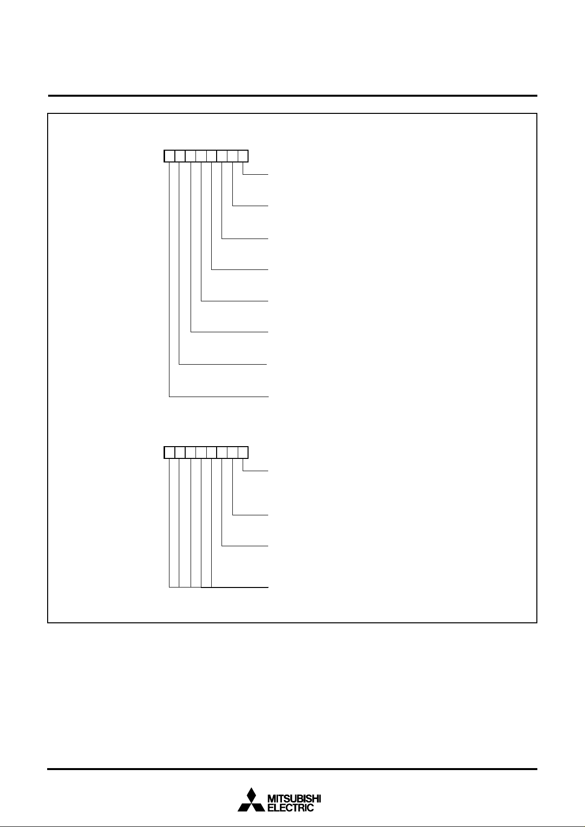
MITSUBISHI MICROCOMPUTERS
P
l l
P
P
b
b
P
P
P
b
b
38K0 Group
SINGLE-CHIP 8-BIT CMOS MICROCOMPUTER
7
0
0 p u l l - u p c o n t r o l r e g i s t e
o r t
( P 0 P U L L : a d d r e s s 0 F F 0
- u p c o n t r o l b i
0
p u
0
r
1 6
)
t
0 : N o p u l l - u p
1 : P u l l - u p
P 0
1
p u l l - u p c o n t r o l b i t
0 : N o p u l l - u p
1 : P u l l - u p
P 0
2
p u l l - u p c o n t r o l b i t
0 : N o p u l l - u p
1 : P u l l - u p
P 0
3
p u l l - u p c o n t r o l b i t
0 : N o p u l l - u p
1 : P u l l - u p
P 0
4
p u l l - u p c o n t r o l b i t
0 : N o p u l l - u p
1 : P u l l - u p
P 0
5
p u l l - u p c o n t r o l b i t
0 : N o p u l l - u p
1 : P u l l - u p
P 0
6
p u l l - u p c o n t r o l b i t
0 : N o p u l l - u p
1 : P u l l - u p
P 0
7
p u l l - u p c o n t r o l b i t
0 : N o p u l l - u p
1 : P u l l - u p
7
0
5 p u l l - u p c o n t r o l r e g i s t e
o r t
( P 5 P U L L : a d d r e s s 0 F F 2
r
1 6
)
50 pull-up control bit
0 : No pull-up
1 : Pull-up
Nothing is arranged for this bit. This is a write disabled bit.
When this bit is read out, the contents are “0”.
P5
2
pull-up co ntrol bit
0 : No pull-up
1 : Pull-up
Nothing is arranged for these bits. These are write disabled
bits. When these bits are read out, the contents are “0”.
Fig. 12 Structure of port I/O-related registers
15
Page 16
MITSUBISHI MICROCOMPUTERS
38K0 Group
SINGLE-CHIP 8-BIT CMOS MICROCOMPUTER
INTERRUPTS
Interrupts occur by fifteen sources: four external, ten internal, and
one software.
Interrupt Control
Each interrupt is controlled by an interrupt request bit, an interrupt
enable bit, and the interrupt disable flag except for the software interrupt set by the BRK instruction. An interrupt occurs if the corresponding interrupt request and enable bits are “1” and the interrupt disable flag is “0”.
Interrupt enable bits can be set or cleared by software.
Interrupt request bits can be cleared by software, but cannot be
set by software.
The BRK instruction cannot be disabled with any flag or bit. The I
flag disables all interrupts except the BRK instruction interrupt.
When several interrupts occur at the same time, the interrupts are
received according to priority.
Interrupt Operation
By acceptance of an interrupt, the following operations are automatically performed:
1. The contents of the program counter and the processor status
register are automatically pushed onto the stack.
2. The interrupt disable flag is set and the corresponding interrupt
request bit is cleared.
3. The interrupt jump destination address is read from the vector
table into the program counter.
■Notes on interrupts
When setting the followings, the interrupt request bit may be set to
“1”.
•When setting external interrupt active edge
Related register:
When not requiring for the interrupt occurrence synchronized with
these setting, take the following sequence.
➀Set the corresponding interrupt enable bit to “0” (disabled).
➁Set the interrupt edge select bit (active edge switch bit).
➂Set the corresponding interrupt request bit to “0” after 1 or more
instructions have been executed.
➃Set the corresponding interrupt enable bit to “1” (enabled).
Interrupt edge selection register (address
0FF316), Timer X mode register (address
002316)
Table 6 Interrupt vector addresses and priority
Interrupt Source
Reset (Note 2)
USB bus reset
USB SOF
USB device
External bus
INT0
Timer X
Timer 1
Timer 2
INT1
(Note 3)
Serial I/O
reception
Serial I/O
transmission
CNTR0
Key-on wake up
A-D conversion
BRK instruction
Notes 1: Vector addresses contain interrupt jump destination addresses.
2: Reset function in the same way as an interrupt with the highest priority.
3: Nothing is arranged in these vector addresses.
4: Fix bit 1 of interrupt control register 2 (address 003F
Priority
1
2
3
4
5
6
7
8
9
10
—
11
12
13
14
15
16
Vector Addresses (Note 1)
High
FFFD16
FFFB16
FFF916
FFF716
FFF516
FFF316
FFF116
FFEF16
FFED16
FFEB16
FFE916
FFE716
FFE516
FFE316
FFE116
FFDF16
FFDD16
Low
FFFC16
FFFA16
FFF816
FFF616
FFF416
FFF216
FFF016
FFEE16
FFEC16
FFEA16
FFE816
FFE616
FFE416
FFE216
FFE016
FFDE16
FFDC16
16) to “0”.
Interrupt Request
Generating Conditions
At reset
At detection of USB bus reset signal (2.5 µs interval SE0)
At detection of USB SOF signal
At detection of resume signal (K state or SE0) or suspend signal (3
ms interval bus idle), or at completion of transaction
At completion of reception or transmission or at completion of DMA
transmission
At detection of either rising or falling edge of INT0 input
At timer X underflow
At timer 1 underflow
At timer 2 underflow
At detection of either rising or falling edge of INT1 input
(Note 4)
At completion of serial I/O data reception
At completion of serial I/O data transmission
At detection of either rising or falling edge of CNTR0 input
At falling of conjunction of input level for port P2 (at input mode)
At completion of A-D conversion
At BRK instruction execution
16
Page 17
t
t
t
b
b
I
I N T
i
( I N T E D G E
)
I
U S B
I
d
(IREQ
C16)
( I C O N
E
)
I
INT
(IREQ
D16)
I
d
(ICON
F16)
F
b7b
b7b
b7b
b7b
U S B
INT
I n t e r r u p t r e q u e s t b i
I n t e r r u p t e n a b l e b i
Interrupt disable flag (I)
MITSUBISHI MICROCOMPUTERS
38K0 Group
SINGLE-CHIP 8-BIT CMOS MICROCOMPUTER
Fig. 13 Interrupt control
7
✽ “0” can be set by software, but “1”
cannot be set .
0
n t e r r u p t e d g e s e l e c t i o n r e g i s t e
: a d d r e s s 0 F F
n t e r r u p t e d g e s e l e c t i o n b i
0
N o t u s e d ( r e t u r n “ 0 ” w h e n r e a d )
I N T
1
i n t e r r u p t e d g e s e l e c t i o n b i t
N o t u s e d ( r e t u r n “ 0 ” w h e n r e a d )
0
n t e r r u p t r e q u e s t r e g i s t e r
1 : address 003
b u s r e s e t i n t e r r u p t r e q u e s t b i
U S B S O F i n t e r r u p t r e q u e s t b i t
U S B d e v i c e i n t e r r u p t r e q u e s t b i t
E X B i n t e r r u p t r e q u e s t b i t
I N T
0
i n t e r r u p t r e q u e s t b i t
T i m e r X i n t e r r u p t r e q u e s t b i t
T i m e r 1 i n t e r r u p t r e q u e s t b i t
T i m e r 2 i n t e r r u p t r e q u e s t b i t
B R K i n s t r u c t i o n
R e s e
I n t e r r u p t r e q u e s t
r
1 6
3
t
a l l i n g e d g e a c t i v
0 :
1 : R i s i n g e d g e a c t i v e
1
e
n t e r r u p t r e q u e s t r e g i s t e r
0
2
2 : address 003
t
1
interrupt request bit
Nothing is arranged for this bit. This is a
write disabled bit. When this bit is read
out, the contents are “0”.
Serial I/O receive interrupt request bit
Serial I/O transmit int erru pt reques t bit
CNTR
0
interrupt request bit
Key- on wake- up interrupt requ est bit
A-D conversion interrupt request bit
Nothing is arranged for this bit. This is a
write disabled bit. When this bit is read
out, the contents are “0”.
0 : No interrupt re quest issue
1 : Interrupt request issued
0
n t e r r u p t c o n t r o l r e g i s t e r
1 : a d d r e s s 0 0 3
b u s r e s e t i n t e r r u p t e n a b l e b i
U S B S O F i n t e r r u p t e n a b l e b i t
U S B d e v i c e i n t e r r u p t e n a b l e b i t
E X B i n t e r r u p t e n a b l e b i t
I N T
0
i n t e r r u p t e n a b l e b i t
T i m e r X i n t e r r u p t e n a b l e b i t
T i m e r 1 i n t e r r u p t e n a b l e b i t
T i m e r 2 i n t e r r u p t e n a b l e b i t
✽ “ 0 ” c a n b e s e t b y s o f t w a r e , b u t “ 1 ”
c a n n o t b e s e t .
Fig. 14 Structure of interrupt-related registers
0
1
1 6
t
nterrupt co ntrol register 2
2 : address 003
1
interrupt enable bit
Fix this bit to “0”.
Serial I/O receive interrupt enable bit
Serial I/O transmit int erru pt enable bit
CNTR
0
interrupt enable bit
Key- on wake- up interrupt enabl e bit
A-D conversion interrupt enab le bit
Fix this bit to “0”.
0 : Interrupts disable
1 : Interrupts enabled
17
Page 18
MITSUBISHI MICROCOMPUTERS
38K0 Group
SINGLE-CHIP 8-BIT CMOS MICROCOMPUTER
Key Input Interrupt (Key-on Wake Up)
A Key-on wake up interrupt request is generated by applying a
falling edge to any pin of port P0 that have been set to input mode.
In other words, it is generated when AND of input level goes from
P o r t P X x
“ L ” l e v e l o u t p u t
P0
P0
P0
7
output
6
output
5
output
P U L L 0 r e g i s t e r
B i t 7 = “ 0 ”
✽
P U L L 0 r e g i s t e r
B i t 6 = “ 0 ”
✽
P U L L 0 r e g i s t e r
B i t 5 = “ 0 ”
✽
✽ ✽
✽ ✽
✽ ✽
P o r t P 0
d i r e c t i o n r e g i s t e r = “ 1 ”
P o r t P 0
7
l a t c h
6
Port P0
latch
P o r t P 0
5
l a t c h
“1” to “0”. An example of using a key input interrupt is shown in
Figure 15, where an interrupt request is generated by pressing
one of the keys consisted as an active-low key matrix which inputs
to ports P00–P03.
7
P o r t P 0
6
d i r e c t i o n r e g i s t e r = “ 1 ”
Port P0
5
direction register = “1”
K e y i n p u t i n t e r r u p t r e q u e s t
P 0
4
o u t p u t
P 0
3
P 0
2
P0
1
0
P 0
i n p u t
i n p u t
input
i n p u t
P U L L 0 r e g i s t e r
B i t 4 = “ 0 ”
✽
P U L L 0 r e g i s t e r
B i t 3 = “ 1 ”
✽
P U L L 0 r e g i s t e r
B i t 2 = “ 1 ”
✽
PULL 0 register
Bit 1 = “1”
✽
P U L L 0 r e g i s t e r
B i t 0 = “ 1 ”
✽
✽ ✽
✽ ✽
✽ ✽
✽ ✽
✽ ✽
P o r t P 0
l a t c h
P o r t P 0
l a t c h
P o r t P 0
l a t c h
P o r t P 0
l a t c h
P o r t P 0
l a t c h
Port P0
4
direction register = “1”
4
P o r t P 0
3
d i r e c t i o n r e g i s t e r = “ 0 ”
3
Port P0
2
direction register = “0”
2
Port P0
1
direction register = “0”
1
0
P o r t P 0
d i r e c t i o n r e g i s t e r = “ 0 ”
0
Port P0
Input reading circuit
Fig. 15 Connection example when using key input interrupt and port P0 block diagram
✽ P - c h a n n e l t r a n s i s t o r f o r p u l l - u p
✽ ✽ C M O S o u t p u t b u f f e r
18
Page 19
MITSUBISHI MICROCOMPUTERS
T i
T i
b
b
38K0 Group
SINGLE-CHIP 8-BIT CMOS MICROCOMPUTER
TIMERS
The 38K0 group has three timers: timer X, timer 1, and timer 2.
The division ratio of each timer or prescaler is given by 1/(n + 1),
where n is the value in the corresponding timer or prescaler latch.
All timers are down count timers. When the timer reaches “0016”,
an underflow occurs at the next count pulse and the corresponding timer latch is reloaded into the timer and the count is continued. When a timer underflows, the interrupt request bit corresponding to that timer is set to “1”.
7
Fig. 16 Structure of timer X mode register
0
m e r X m o d e r e g i s t e
( T M : a d d r e s s 0 0 2 3
i n t e r r u p t
m e r X o p e r a t i n g m o d e b i t
i n t e r r u p
a c t i v e e d g e s w i t c h b i
b 1 b 0
00 : T i m e r m o d e
01 : P u l s e o u t p u t m o d e
10 : E v e n t c o u n t e r m o d e
11 : P u l s e w i d t h m e a s u r e m e n t m o d e
0
C N T R
0 : F a l l i n g e d g e a c t i v e f o r C N T R
C o u n t a t r i s i n g e d g e i n e v e n t c o u n t e r m o d e
1 : R i s i n g e d g e a c t i v e f o r C N T R
C o u n t a t f a l l i n g e d g e i n e v e n t c o u n t e r m o d e
T i m e r X c o u n t s t o p b i t
0 : C o u n t s t a r t
1 : C o u n t s t o p
N o t u s e d ( r e t u r n “ 0 ” w h e n r e a d )
r
1 6)
s
t
0
0
t
Timer 1 and Timer 2
The count source of prescaler 12 is the system clock divided by
16. The output of prescaler 12 is counted by timer 1 and timer 2,
and a timer underflow periodically sets the interrupt request bit.
Timer X
Timer X can each select in one of four operating modes by setting
the timer X mode register.
(1) Timer Mode
The timer counts the count source selected by timer count source
selection bit.
(2) Pulse Output Mode
The timer counts the system clock divided by 16. Whenever the
contents of the timer reach “0016”, the signal output from the
CNTR0 pin is inverted. If the CNTR0 active edge selection bit is
“0”, output begins at “ H”.
If it is “1”, output starts at “L”. When using a timer in this mode, set
the corresponding port P51 direction register to output mode.
(3) Event Counter Mode
Operation in event counter mode is the same as in timer mode,
except that the timer counts signals input through the CNTR0 pin.
When the CNTR0 active edge selection bit is “0”, the rising edge of
the CNTR0 pin is counted.
When the CNTR0 active edge selection bit is “1”, the falling edge
of the CNTR0 pin is counted.
(4) Pulse Width Measurement Mode
If the CNTR0 active edge selection bit is “0”, the timer counts the
system clock divided by 16 while the CNTR0 pin is at “H”. If the
CNTR0 active edge selection bit is “1”, the timer counts it while the
CNTR0 pin is at “L”.
The count can be stopped by setting “1” to the timer X count stop
bit in any mode. The corresponding interrupt request bit is set
each time a timer underflows.
19
Page 20
e a s u r e m e n t
D a t a b u s
MITSUBISHI MICROCOMPUTERS
38K0 Group
SINGLE-CHIP 8-BIT CMOS MICROCOMPUTER
P 5
1
/ C N T R
S y s t e m c l o c k
0
1
Port P5
direction
register
S y s t e m c l o c k
D i v i d e r
1 / 1 6
C N T R
0
a c t i v e
e d g e s e l e c t i o n b i t
“ 0 ”
“ 1 ”
P o r t P 5
l a t c h
P u l s e o u t p u t m o d e
D i v i d e r
1 / 1 6
P u l s e w i d t h
m
m o d e
CNTR
edge selection bit
1
Prescaler 12 latch (8)
E v e n t
c o u n t e r
m o d e
0
active
P r e s c a l e r 1 2 ( 8 )
Timer mode
Pulse output
mode
T i m e r X c o u n t s t o p b i t
P r e s c a l e r X l a t c h ( 8 )
“ 1 ”
Q
Q
“0”
Data bus
Prescaler X (8)
Toggle
flip-flop
T
R
Timer 1 latch (8)
Timer 1 (8)
Timer X latch (8)
Timer X (8)
Timer X latch write
Pulse output mode
Timer 2 latch (8)
Timer 2 (8)
T i m e r X i n t e r r u p t
r e q u e s t b i t
C N T R
0
i n t e r r u p t
r e q u e s t b i t
T i m e r 2 i n t e r r u p t
r e q u e s t b i t
Fig. 17 Timer block diagram
T i m e r 1 i n t e r r u p t
r e q u e s t b i t
20
Page 21
MITSUBISHI MICROCOMPUTERS
P
EXT C
S
P
EXA
S
P
EXD R E Q
D
S
k
F/F
r
A d d
R
)
R
(RI)
S h i f
k
S
Add
B R G
D
Add
Shif
k
T
)
T
(TBE)
T
(TI)
T
Add
D
A d d
P
EXDACK/TxD
R
S
D
D0D1D2D3D4D5D
R B F
T B E
T B E
T
hif
k
Serial
TXD
S
RXD
W
O
(OE)
N
T h
D
D0D
D
D3D4D5D
38K0 Group
SINGLE-CHIP 8-BIT CMOS MICROCOMPUTER
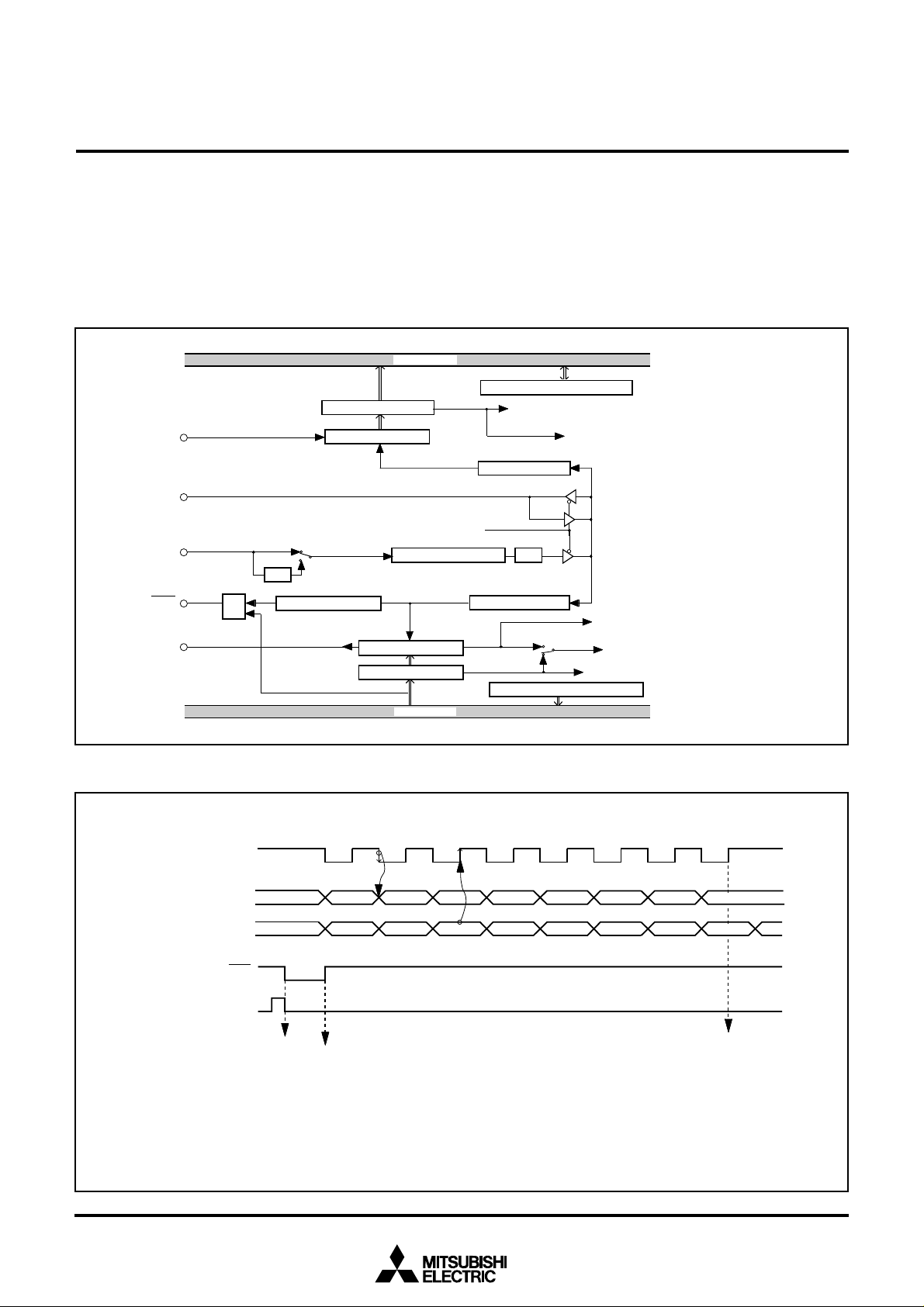
SERIAL I/O
Serial I/O can be used as either clock synchronous or asynchronous (UART) serial I/O. A dedicated timer (baud rate generator) is
also provided for baud rate generation.
ata bus
r e s s 0 0 2
R e c e i v e b u f f e r r e g i s t e r
/ R x
0
/
4
2
/
/
4
C L K
c o u n t s o u r c e s e l e c t i o n b i
y s t e m c l o c
1 / 4
3
/
1
/
4
R D Y
F a l l i n g - e d g e d e t e c t o r
41/
R e c e i v e s h i f t r e g i s t e r
t c l o c
e r i a l I / O s y n c h r o n o u
c l o c k s e l e c t i o n b i t
F r e q u e n c y d i v i s i o n r a t i o 1 / ( n + 1 )
t
Transmit shift register
Transmit buffer regis ter
B a u d r a t e g e n e r a t o r
ata bus
6
1 6
ress 0FE2
t cloc
ress 0026
(1) Clock Synchronous Serial I/O Mode
Clock synchronous serial I/O mode can be selected by setting the
mode selection bit of the serial I/O control register (bit 6 of address 0FE016) to “1”.
For clock synchronous serial I/O, the transmitter and the receiver
must use the same clock. If an internal clock is used, transfer is
started by a write signal to the Trancemit/Receive buffer register.
S e r i a l I / O c o n t r o l r e g i s t e r
e c e i v e b u f f e r f u l l f l a g ( R B F
eceive interrupt re qu es t
Clock control circuit
s
1/4
16
Clock control circuit
ransmit interrupt source selection bit
ransmit buffer empty flag
Serial I/ O status regi s te
16
r e s s 0 F E
r a n s m i t s h i f t r e g i s t e r s h i f t c o m p l e t i o n f l a g ( T S C
ransmit interrupt request
ress 0027
1 6
0
16
Fig. 18 Block diagram of clock synchronous serial I/O
ransfer s
(1/2 to 1/2048 of the internal
clock, or an external clock)
e c e i v e e n a b l e s i g n a l
r i t e s i g n a l t o r e c e i v e / t r a n s m i t
b u f f e r r e g i s t e r ( a d d r e s s 0 0 2 6
t cloc
output
e r i a l i n p u t
R D Y
1 6
)
=
0
=
1
T S C = 0
o t e
e t r a n s m i t i n t e r r u p t ( T I ) c a n b e g e n e r a t e d e i t h e r w h e n t h e t r a n s m i t b u f f e r r e g i s t e r h a s e m p t i e d ( T B E = 1 ) o r a f t e r t h e t r a n s m i t
s
1 :
s h i f t o p e r a t i o n h a s e n d e d ( T S C = 1 ) , b y s e t t i n g t h e t r a n s m i t i n t e r r u p t s o u r c e s e l e c t i o n b i t ( T I C ) o f t h e s e r i a l I / O 1 c o n t r o l r e g i s t e r .
2 : I f d a t a i s w r i t t e n t o t h e t r a n s m i t b u f f e r r e g i s t e r w h e n T S C = 0 , t h e t r a n s m i t c l o c k i s g e n e r a t e d c o n t i n u o u s l y a n d s e r i a l d a t a i s
o u t p u t c o n t i n u o u s l y f r o m t h e T
3 : T h e r e c e i v e i n t e r r u p t ( R I ) i s s e t w h e n t h e r e c e i v e b u f f e r f u l l f l a g ( R B F ) b e c o m e s “ 1 ” .
X
D p i n .
1
Fig. 19 Operation of clock synchronous serial I/O function
6
2
6
7
7
=
T S C = 1
verrun error
detection
1
21
Page 22
MITSUBISHI MICROCOMPUTERS
S
k
OE
PE
F E
D
R
Add
R
hif
R
)
R
)
B
F
)
Add
D
T
hif
Add
T
hif
hif
(TSC)
T
(TBE)
T
(TI)
A d d
S T d
SP d
UART
Add
Ch
A d d
B R G
t
T
bit
S
C l
C h
Serial I/O
P
EXT C
S
K
Serial I/O
P
EXD R E Q
D
P
EXDACK/TxD
T S C
R B F
T B E
TBE
RBF
RBF
S T
D0D
S P
D
0
D
S T
S P
TBE
S T
D0D
S P
D0D
S T
S P
T
l
b i
E
N
S
TXD
S
RXD
R
l
T
k
38K0 Group
SINGLE-CHIP 8-BIT CMOS MICROCOMPUTER
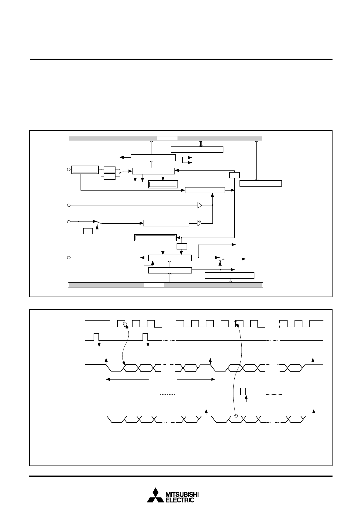
(2) Asynchronous Serial I/O (UART) Mode
Clock asynchronous serial I/O mode (UART) can be selected by
setting the serial I/O mode selection bit of the serial I/O control
register to “0”.
Eight serial data transfer formats can be selected, and the transfer
formats used by a transmitter and receiver must be identical.
The transmit and receive shift registers each have a buffer regis-
a t a b u
ress 0026
a r a c t e r l e n g t h s e l e c t i o n b i
/ R x
0
/
4
e t e c t o
r
7 b i t s
8 bits
e r i a l I / O s y n c h r o n o u s c l o c k s e l e c t i o n b i
/
2
/
4
C L
c o u n t s o u r c e s e l e c t i o n b i
y s t e m c l o c
1 / 4
41/
aracter length selection bit
16
eceive buffer register
t
eceive s
t register
etector
r e q u e n c y d i v i s i o n r a t i o 1 / ( n + 1
a u d r a t e g e n e r a t o
ress 0FE2
ST/SP/PA generator
ransmit s
Transmi t buffer register
ata bus
ter, but the two buffers have the same address in memory. Since
the shift register cannot be written to or read from directly, transmit
data is written to the transmit buffer, and receive data is read from
the receive buffer.
The transmit buffer can also hold the next data to be transmitted,
and the receive buffer register can hold a character while the next
character is being received.
s
t
r
16
1/16
t register
ress 0026
1 control register
e c e i v e b u f f e r f u l l f l a g ( R B F
r e s s 0 F E
e c e i v e i n t e r r u p t r e q u e s t ( R I
o c k c o n t r o l c i r c u i
t
ransmit interrupt source selection
16
status register
1/16
1 6
0
control register
ress 0FE1
ransmit s
t register s
ransmit interrupt request
ransmit buffer empty flag
r e s s 0 0 2
7
16
t completion flag
1 6
Fig. 20 Block diagram of UART serial I/O
r a n s m i t o r r e c e i v e c l o c
ransmit buffer write signa
=
0
=
0
T B E = 1
e r i a l o u t p u t
e c e i v e b u f f e r r e a d s i g n a
e r i a l i n p u t
r r o r f l a g d e t e c t i o n o c c u r s a t t h e s a m e t i m e t h a t t h e R B F f l a g b e c o m e s “ 1 ” ( a t 1 s t s t o p b i t , d u r i n g r e c e p t i o n )
o t e s
1 :
2 : T h e t r a n s m i t i n t e r r u p t ( T I ) c a n b e g e n e r a t e d t o o c c u r w h e n e i t h e r t h e T B E o r T S C f l a g b e c o m e s “ 1 ” , d e p e n d i n g o n t h e s e t t i n g o f t h e t r a n s m i t i n t e r r u p t
s o u r c e s e l e c t i o n b i t ( T I C ) o f t h e s e r i a l I / O 1 c o n t r o l r e g i s t e r .
3 : T h e r e c e i v e i n t e r r u p t ( R I ) i s s e t w h e n t h e R B F f l a g b e c o m e s “ 1 ” .
4 : A f t e r d a t a i s w r i t t e n t o t h e t r a n s m i t b u f f e r r e g i s t e r w h e n T S C = 1 , 0 . 5 t o 1 . 5 c y c l e s o f t h e d a t a s h i f t c y c l e i s n e c e s s a r y u n t i l c h a n g i n g t o T S C = 0 .
Fig. 21 Operation of UART serial I/O function
=0
1
t
1 s t a r t
7 o r 8 d a t a b i t s
1 o r 0 p a r i t y b i t
1 o r 2 s t o p b i t ( s )
1
=1
1
✽
G e n e r a t e d a t 2 n d b i t i n 2 - s t o p - b i t m o d e
=
=1
0
1
.
T S C = 1
✽
=1
22
Page 23

[Serial I/O Control Register (SIOCON)] 0FE016
The serial I/O control register contains eight control bits for the serial I/O function.
[UART Control Register (UARTCON)] 0FE116
The UART control register consists of four control bits (bits 0 to 3)
which are valid when asynchronous serial I/O is selected and set
the data format of an data transfer.
[Serial I/O Status Register (SIOSTS)] 002716
The read-only serial I/O status register consists of seven flags
(bits 0 to 6) which indicate the operating status of the serial I/O
function and various errors.
Three of the flags (bits 4 to 6) are valid only in UART mode.
The receive buffer full flag (bit 1) is cleared to “0” when the receive
buffer is read.
If there is an error, it is detected at the same time that data is
transferred from the receive shift register to the receive buffer register, and the receive buffer full flag is set. A write to the serial I/O
status register clears all the error flags OE, PE, FE, and SE (bit 3
to bit 6, respectively). Writing “0” to the serial I/O enable bit SIOE
(bit 7 of the serial I/O control register) also clears all the status
flags, including the error flags.
All bits of the serial I/O status register are initialized to “0” at reset,
but if the transmit enable bit (bit 4) of the serial I/O control register
has been set to “1”, the transmit shift register shift completion flag
(bit 2) and the transmit buffer empty flag (bit 0) become “1”.
MITSUBISHI MICROCOMPUTERS
38K0 Group
SINGLE-CHIP 8-BIT CMOS MICROCOMPUTER
[Transmit Buffer/Receive Buffer Register (TB/
RB)] 0026
The transmit buffer register and the receive buffer register are located at the same address. The transmit buffer register is writeonly and the receive buffer register is read-only. If a character bit
length is 7 bits, the MSB of data stored in the receive buffer register is “0”.
16
[Baud Rate Generator (BRG)] 0FE216
The baud rate generator determines the baud rate for serial transfer.
The baud rate generator divides the frequency of the count source
by 1/(n + 1), where n is the value written to the baud rate generator.
■Notes on serial I/O
When setting the transmit enable bit to “1”, the serial I/O transmit
interrupt request bit is automatically set to “1”. When not requiring
the interrupt occurrence synchronized with the transmission
enalbed, take the following sequence.
➀Set the serial I/O transmit interrupt enable bit to “0” (disabled).
➁Set the transmit enable bit to “1”.
➂Set the serial I/O transmit interrupt request bit to “0” after 1 or
more instructions have been executed.
➃Set the serial I/O transmit interrupt enable bit to “1” (enabled).
23
Page 24
MITSUBISHI MICROCOMPUTERS
BRG
(CSS)
S
T
)
Serial I/O
U A R T
C h
)
38K0 Group
SINGLE-CHIP 8-BIT CMOS MICROCOMPUTER
b 7b
0
(SIOSTS : address 0027
r a n s m i t b u f f e r e m p t y f l a g ( T B E
0 : B u f f e r f u l l
1 : B u f f e r e m p t y
R e c e i v e b u f f e r f u l l f l a g ( R B F )
0 : B u f f e r e m p t y
1 : B u f f e r f u l l
T r a n s m i t s h i f t r e g i s t e r s h i f t c o m p l e t i o n f l a g ( T S C )
0 : T r a n s m i t s h i f t i n p r o g r e s s
1 : T r a n s m i t s h i f t c o m p l e t e d
O v e r r u n e r r o r f l a g ( O E )
0 : N o e r r o r
1 : O v e r r u n e r r o r
P a r i t y e r r o r f l a g ( P E )
0 : N o e r r o r
1 : P a r i t y e r r o r
F r a m i n g e r r o r f l a g ( F E )
0 : N o e r r o r
1 : F r a m i n g e r r o r
S u m m i n g e r r o r f l a g ( S E )
0 : ( O E ) U ( P E ) U ( F E ) = 0
1 : ( O E ) U ( P E ) U ( F E ) = 1
N o t u s e d ( r e t u r n s “ 1 ” w h e n r e a d )
b 7b
c o n t r o l r e g i s t e r
0
( U A R T C O N : a d d r e s s 0 F E 1
a r a c t e r l e n g t h s e l e c t i o n b i t ( C H A S
0 : 8 b i t s
1 : 7 b i t s
P a r i t y e n a b l e b i t ( P A R E )
0 : P a r i t y c h e c k i n g d i s a b l e d
1 : P a r i t y c h e c k i n g e n a b l e d
P a r i t y s e l e c t i o n b i t ( P A R S )
0 : E v e n p a r i t y
1 : O d d p a r i t y
S t o p b i t l e n g t h s e l e c t i o n b i t ( S T P S )
0 : 1 s t o p b i t
1 : 2 s t o p b i t s
N o t u s e d ( r e t u r n “ 0 ” w h e n r e a d )
( T h i s i s a w r i t e d i s a b l e d b i t . )
N o t u s e d ( r e t u r n “ 1 ” w h e n r e a d )
status register
b7 b0
16
)
1 6
)
e r i a l I / O c o n t r o l r e g i s t e
( S I O C O N : a d d r e s s 0 F E 0
count source selection bit
0: System clock
1: System clock/4
Serial I/O synchronous clock selection bit (SCS)
0: BRG output divided by 4 when clock synchronous serial
I/O is selected.
BRG output divided by 16 when UART is selected.
1: External clock input when clock synchronous serial I/O is
selected.
External clock input divided by 16 when UART is selected.
RDY
output enable bit (SRDY)
S
3
pin operates as ordinary I/O pin
0: P4
1: P4
3
pin operate s as S
Transmit interrupt source selection bit (TIC)
0: Interrupt when transmit buffer has emptied
1: Interrupt when transmit shift operation is completed
Transmit enable bit ( TE)
0: Transmit disabled
1: Transmit enabled
Receive enable bit (RE)
0: Receive disabled
1: Receive enabled
Serial I/O mode selection bi t (SIOM)
0: Asynchronous serial I/O (UART)
1: Clock synchronous serial I/O
Serial I/O enable bit (SIOE)
0: Serial I/O disabled
0
(pins P4
1: Serial I/O enabled
0
(pins P4
r
1 6
)
RDY
output pin
–P43 operate as ordinary I/O pins)
–P43 can operate as serial I/O pins)
Fig. 22 Structure of serial I/O control registers
24
Page 25
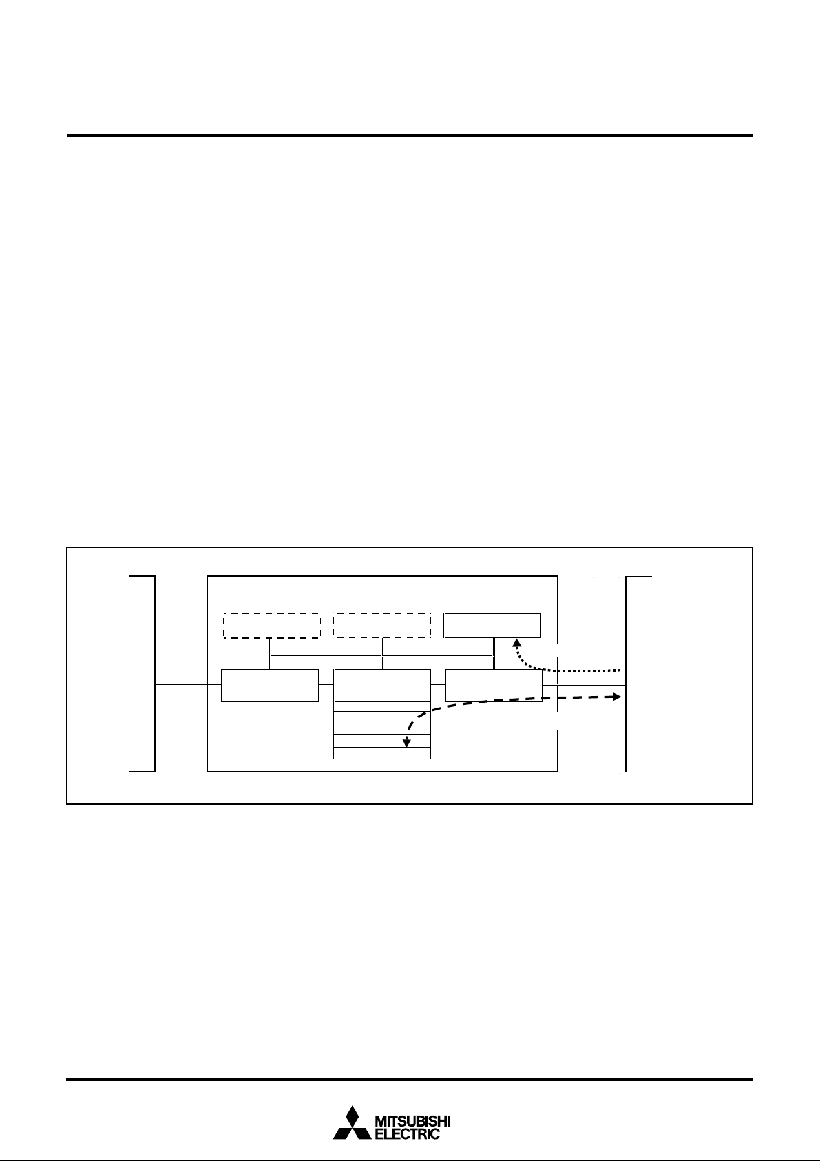
MITSUBISHI MICROCOMPUTERS
38K0 Group
SINGLE-CHIP 8-BIT CMOS MICROCOMPUTER
USB FUNCTION
38K0 Group is equipped with a USB function control circuit
(USBFCC) that enables effective interfacing with the host-PC.
This circuit is in compliance with USB Specification Version 2.0
Full-Speed Transfer Mode (12 Mbps, equivalent to Version 1.1).
This circuit also supports all four transfer-types specified in the
standard USB specification.
The USBFCC has four endpoints that can select its transfer type.
Although Endpoint 0 is fixed to Control Transfer, the Endpoints 1
to 3 can be set to Interrupt Transfer, Bulk Transfer, or Isochronous
Transfer.
A dedicated circuit automatically performs stage management for
Control Transfer and packet management for transactions, which
are necessary for matching of data transmit/receive timing, error
detection, and retry after error. This dedicated control circuit enables the user to develop a program or timing design very easily.
Each endpoint can be programmed for data transfer conditions so
that the endpoints are adaptive for all USB device class transfer
systems.
The data buffer of each endpoint can be assigned to any area in
the multi-channel RAM. This feature offers highly efficient memory
usage by avoiding re-buffering and enabling simple data modification.
The transmit/receive data is directly transferred to the data buffer
via the control circuit (direct RAM access type) without disturbing
the CPU operation. This mechanism enables the CPU to transfer
data smoothly with no drop in performance. In addition to this
buffer function, a double-buffer setting will keep a re-buffering stall
at a minimum and increase the overall data throughput (max. 64
bytes X 2 channels).
As other special signals control, the endpoints have detection
functions for the USB bus reset signal, resume signal, suspend
signal, and SOF signal, and also have a remote wake-up signal
transmit function.
When completing data transfer or receiving a special signal, the
endpoint generates the corresponding interrupt to the CPU (3 vectors/18 factors).
With all this essential yet comprehensive built-in hardware, your
system using the 38K2 group will be ready for any USB application that comes its way.
38K0 Group MCU
External MCU
Built-in Peripheral
Functions
External Bus Interface
(EXB)
Program ROM
Fig. 23 USB function overview
USB Data Transfer
The USB specification promises 12 Mbps data transfer in the fullspeed mode, that is equivalent to 1.5 M bytes per second of data
transactions.
However, in USB data transfer, bit-stuffing may be executed depending on the bit patterns of the transfer data, possibly resulting
in 1-byte data (normally 8 bits) handled as up to 10 bits.
Because USB uses asynchronous transfers, the clock cycle of the
USB internal reference clock may change to adjust to the clock
phase. Therefore, the access timing of the USBFCC for the multichannel RAM will change owing to the frequency of internal clock φ:
When the USBFCC is operating at φ =8 MHZ, access for a normal
CPU
Interrupt request
USBMulti-channel RAM
Data transmit/Receive path
[Direct RAM Access Type]
USB Bus
(USB-Host)
transfer is performed every 5 to 6 cycles and access for a bit-stuffing transfer is performed in up to 7 cycles.
If the EXB function is enabled in the above conditions, this function generates a maximum wait of 1 clock cycle, so that the
access is performed every 4 to 8 cycles.
When operating at φ = 6MHZ, a normal access is performed every
4 cycles. If the clock-phase correction of the reference clock occurs, access is performed every 3 to 5 cycles.
If bit stuffing occurs at this clock rate, the access cycle will be extended to up to 6 cycles. When the EXB function that generates a
maximum 1-wait cycle is used in this condition, the access cycle
will be 2 (min.) to 7 (max.) cycles.
25
Page 26
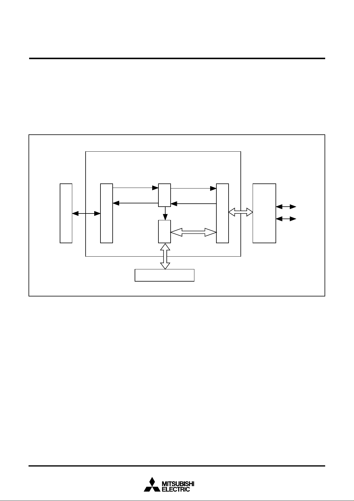
USB Function Control Circuit (USBFCC)
Block Diagram
The following diagram shows the USBFCC block diagram. The circuit comprises:
(1) Serial Interface Engine (SIE)
(2) Device Control Unit (DCU)
(3) Internal Memory Interface (MIF)
(4) CPU Interface (CIF)
U S B F u n c t i o n C o n t r o l C i r c u i t
MITSUBISHI MICROCOMPUTERS
38K0 Group
SINGLE-CHIP 8-BIT CMOS MICROCOMPUTER
D C U c o n t r o l
U
D
D C U s t a t u s
U
C
P
F
C
I
MIF control
C
F
M
I
M u l t i - C h a n n e l R A M
Fig. 24 USB Function Control Circuit (USBFCC) block diagram
(1) Serial Interface Engine (SIE)
The SIE performs the following USB lower-layer protocols (packets, transactions):
•Sampling of receive data and clock, generation of transmit clock
•Serial-to-parallel conversion of transmit/receive data
•NRZI (Non Return Zero Invert) encode/decode
•Bit stuffing/unstuffing
•SYNC (Synchronization Pattern) detection, EOP (End of
Packet) detection
•USB address detection, endpoint detection
•CRC (Cyclic Redundancy Check) generation and checking
SIE control
r
S I E s t a t u s
E
S
I
D 0 +
D 0 -
U
S B T r a n s c e i v e
Transmit/Receive
data
(3) Memory Interface (MIF)
The MIF controls the flow of data transfer between the SIE and the
multi-channel RAM under the management of the DCU.
(4) CPU Interface (CIF)
The CIF performs the following functions:
•Mode setting via registers, DCU control signal generation, DCU
status signal reading
•Interrupt signal generation
•Internal bus interface control.
(2) Device Control Unit (DCU)
The DCU manages the following USB upper-layer protocols (address/endpoint and control-transfer sequence):
•Status control for each endpoint
•Control-transfer sequence control
•Memory interface status control
26
Page 27
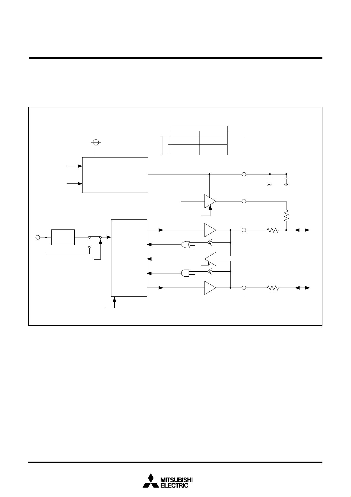
USB Port External Circuit Configuration
Full
Full
The operation mode of the USB port driver circuit can be configured by USB control register (address 001016).
Figure 25 shows the USB port external circuit block diagram.
D V
C C
R E F
V
R E F E
U S B R e f e r e n c e
V
R E F C O N
V o l t a g e C i r c u i t
0
E
1
V
3.3V output
Normal mode
MITSUBISHI MICROCOMPUTERS
SINGLE-CHIP 8-BIT CMOS MICROCOMPUTER
VREFCON
01
Hiz Hiz
3.3V output
Low-power mode
USBVREF status
USBVREF
2 . 2 µF
38K0 Group
0 . 1 µF
T R O N C O N
TRONE
X
OUT
PLL
“1”
f
VCO
UCLKCON
“ 0 ”
f
U S B
USB
Module
USBE
USBDIFE
USBE
USBE
Fig. 25 USB port external circuit (D0+, D0-, USBVREF, TrON) block diagram
Speed
Speed
T R O N
1.5 kΩ
D 0 +
+
-
D 0 -
2 7 Ω
2 7 Ω
27
Page 28
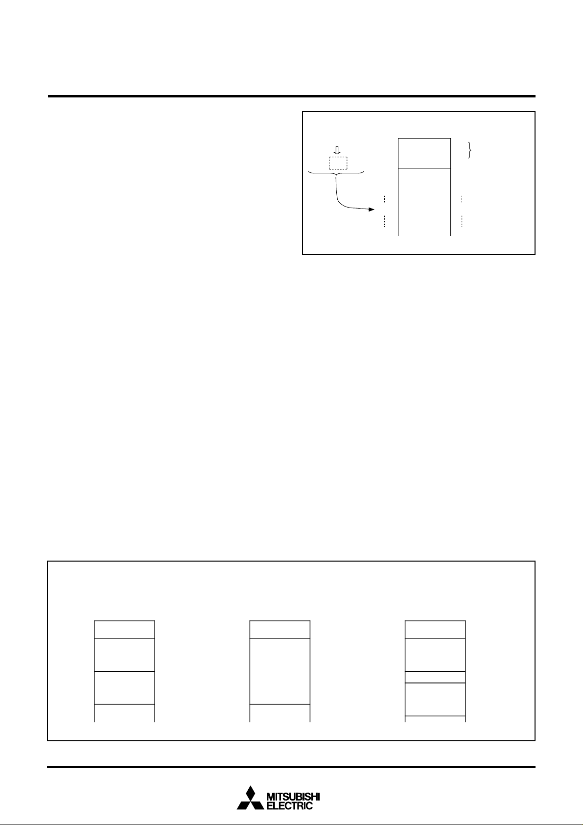
MITSUBISHI MICROCOMPUTERS
38K0 Group
SINGLE-CHIP 8-BIT CMOS MICROCOMPUTER
Endpoint Buffer Area Setting
The buffer area used in data transfer can be assigned to any area
of the multi-channel RAM for each endpoint.
●Buffer area beginning address
The buffer area configuration register (address 0FED16) defines
the beginning address of the buffer area (every 32 bytes) for each
Endpoint. However, the only RAM area is configurable.
•00h [Address 000016], 01h [Address 002016]: Not configurable
•02h [Address 004016] to 1Fh [Address 03E016]: Configurable
●Interrupt-source dependant buffer area offset address
An offset value is added to the beginning address of each source,
which is specified by the interrupt source register (address
001D16), for each endpoint.
This section describes in detail the beginning address specified by
the buffer area set register as offset address 00h, according to
each endpoint.
(1) Endpoint 00
Endpoint 00 has two kinds of interrupt sources for accessing the
buffer. The respective address offsets are:
•BSRDY00 (SETUP Buffer Ready Interrupt): Offset address = 00h
•BRDY00 (OUT or IN Buffer Ready Interrupt):
Offset address = 08h
(2) Endpoint 01
The buffer area offset address for each interrupt source for of Endpoint 01 varies according to the contents of the EP01 set register
(address 001916).
•In single buffer mode (DBLB01 = “0”):
Endpoint 01 has only one interrupt source for accessing the
buffer.
B0RDY01 (Buffer 0 Ready Interrupt): Offset address = 00h
0000
0FED
16
0010 1010
= 15h
0000
Memory
0000
0020
0040
0060
02A0
03E0
16
SFR
16
16
16
RAM
16
16
0FED
16
00
Disabled to be used
01
02
03
15
1F
Fig. 26 Example setting of buffer area beginning address
•In double buffer mode (DBLB01 = “1”):
Endpoint 01 has two kinds of interrupt sources for accessing the
buffer.
B0RDY01 (Buffer 0 Ready Interrupt): Offset address = 00h
B1RDY01 (Buffer 1 Ready Interrupt):
The offset address varies according to the double buffer beginning address set bit (BSIZ01).
-Offset address = 08h when BSIZ01 = 00
-Offset address = 10h when BSIZ01 = 01
-Offset address = 40h when BSIZ01 = 10
-Offset address = 80h when BSIZ01 = 11
(3) Endpoints 02 and 03
Same as Endpoint 01.
Notes
The selected RAM area must be within addresses 004016 to
03FF16.
Make sure the buffer area beginning address is set in agreement
with the offset address and the number of transmit/receive data
bytes.
This is particularly important when in the double buffer mode or
when handling 64-byte data.
(a) When selecting Endpoint 00
Memory
16
02A0
Offset
00
h
(b) When selecting Single Buffer Mode
Memory
02A016
Offset
00h
BSRDY00
02A816
08h
B0RDY01
BRDY00
Fig. 27 Examples of interrupt source dependant buffer area offset address
(c) When selecting Double Buffer Mode
(when BSIZ01 = 11)
Memory
02A016
Offset
00h
B0RDY01
032016
80h
B1RDY01
28
Page 29

USB Interrupt Function
USB Interrupt Control Circuit (USBINTCON) has 3 requests and
16 USB-device interrupt request sources. Each interrupt source
register enables the user to easily determine which interrupt has
occurred.
Table 7 shows the list of USB interrupt sources.
Table 7 USB interrupt sources
Interrupt request bit
(IREQ1: Address 003C16)
USB bus reset
USB SOF —
USB device EP00
USB interrupt bit
(USBIREQ: Address 001716)
—
EP01
EP02
EP03
SUS
RSM
At USB bus reset signal detection:
After enabling the USB module (USBE = “1”), an interrupt request occurs
when 2.5 µs SE0 state is detected in D0+/D0- port.
(Equivalent to 120-clock length when fUSB = 48 MHz)
At SOF packet receive:
After enabling the USB module (USBE = “1”), an interrupt request occurs
when SOF packet is detected in D0+/D0- port.
Its occurrence does not depend on frame-time or CRC value after SOF
packet is transferred.
(Normally, SOF packet detection occurs only when fUSB = 48 MHz)
At Endpoint 00 data transfer complete:
•Buffer ready (read/write enabled state)
•Control transfer completed
•Status stage transition
•SETUP buffer ready (read enabled state)
•Control transfer error
At Endpoint 01 data transfer complete:
•Buffer 0 ready (read/write enabled state)
•Buffer 1 ready (read/write enabled state)
•Transfer error
At Endpoint 02 data transfer complete:
•Buffer 0 ready (read/write enabled state)
•Buffer 1 ready (read/write enabled state)
•Transfer error
At Endpoint 03 data transfer complete:
•Buffer 0 ready (read/write enabled state)
•Buffer 1 ready (read/write enabled state)
•Transfer error
At suspend signal detection:
After enabling the USB module (USBE = “1”), an interrupt request occurs
when 3 ms J state is detected in D0+/D0- port.
(Equivalent to 144,000 clock-length when fUSB = 48MHz)
At resume signal detection:
After enabling the USB module (USBE = “1”) and resume interrupt (RSME
= “1”), an interrupt request occurs when a bus state change (J state to
SE0 or K state) is detected in D0- port.
MITSUBISHI MICROCOMPUTERS
38K0 Group
SINGLE-CHIP 8-BIT CMOS MICROCOMPUTER
Interrupt source
29
Page 30
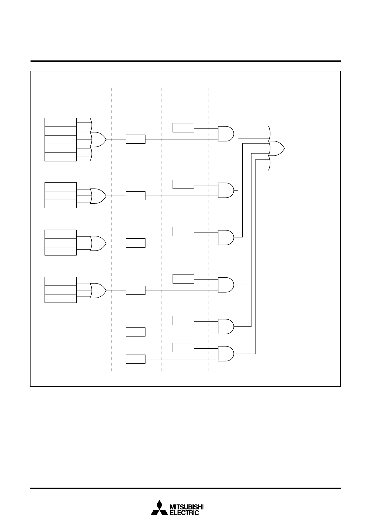
MITSUBISHI MICROCOMPUTERS
38K0 Group
SINGLE-CHIP 8-BIT CMOS MICROCOMPUTER
[EPXXREG5]
[EP00REQ]
BRDY00
CTEND00
CTSTS00
BSYDY00
ERR00
[EP01REQ]
B0RDY01
B1RDY01
ERR01
[EP02REQ]
B0RDY02
B1RDY02
ERR02
[EP03REQ]
B0RDY03
B1RDY03
ERR03
[USBIREQ]
EP00
EP01
EP02
EP03
[USBICON]
EP00E
USB device
interrupt request
EP01E
EP02E
EP03E
Fig. 28 USB device interrupt control
SUSE
SUS
RSME
RSM
30
Page 31
USB Register List
The USB register list is shown below.
MITSUBISHI MICROCOMPUTERS
38K0 Group
SINGLE-CHIP 8-BIT CMOS MICROCOMPUTER
0010
0011
0012
0013
0014
0015
0016
0017
0018
0019
001A
001B
001C
001D
001E
001F
0FEC
0FED
(1) Endpoint 00
0019
001A
001B
001C
001D
001E
001F
0FEC
0FED
(2) Endpoint 01
0019
001A
001B
001C
001D
001E
001F
0FEC
0FED
(3) Endpoint 02
0019
001A
001B
001C
001D
001E
001F
0FEC
0FED
(4) Endpoint 03
0019
001A
001B
001C
001D
001E
001F
0FEC
0FED
16
USB control register
16
USB Function enable register
16
USB function address register
16
16
Frame number register Low
16
Frame number register High
16
USB interrupt source enable register
16
USB interrupt source register
16
Endpoint index register
16
Endpoint field register 1
16
Endpoint field register 2
16
Endpoint field register 3
16
Endpoint field register 4
16
Endpoint field register 5
16
Endpoint field register 6
16
Endpoint field register 7
16
Endpoint field register 8
16
Endpoint field register 9
16
EP00 stage register
16
EP00 control register 1
16
EP00 control register 2
16
EP00 control register 3
16
EP00 interrupt source register
16
EP00 transmit/receive byte number register
16
16
16
EP00 buffer area set register
16
EP01 set register
16
EP01 control register 1
16
EP01 control register 2
16
EP01 control register 3
16
EP01 interrupt source register
16
EP01 byte number register 0
16
EP01 byte number register 1
16
EP01 MAX. packet size register
16
EP01 buffer area set register
16
EP02 set register
16
EP02 control register 1
16
EP02 control register 2
16
EP02 control register 3
16
EP02 interrupt source register
16
EP02 byte number register 0
16
EP02 byte number register 1
16
EP02 MAX. packet size register
16
EP02 buffer area set register
16
EP03 set register
16
EP03 control register 1
16
EP03 control register 2
16
EP03 control register 3
16
EP03 interrupt source register
16
EP03 byte number register 0
16
EP03 byte number register 1
16
EP03 MAX. packet size register
16
EP03 buffer area set register
SYMBOLAddress Register Name
USBCON
USBAE
USBA0
FNUML
FNUMH
USBICON
USBIREQ
USBINDEX
EPXXREG1
EPXXREG2
EPXXREG3
EPXXREG4
EPXXREG5
EPXXREG6
EPXXREG7
EPXXREG8
EPXXREG9
EP00STG
EP00CON1
EP00CON2
EP00CON3
EP00REQ
EP00BYT
EP00BUF
EP01CFG
EP01CON1
EP01CON2
EP01CON3
EP01REQ
EP01BYT0
EP01BYT1
EP01MAX
EP01BUF
EP02CFG
EP02CON1
EP02CON2
EP02CON3
EP02REQ
EP02BYT0
EP02BYT1
EP02MAX
EP02BUF
EP03CFG
EP03CON1
EP03CON2
EP03CON3
EP03REQ
EP03BYT0
EP03BYT1
EP03MAX
EP03BUF
bit 7 bit 6
USBE UCLKCON
RSME SUSE EP03E EP02E EP01E EP00E
RSM SUS EP03 EP02 EP01 EP00
bit 5
USBDIFE
USB SFR
bit 4 bit 3 bit 2 bit 1 bit 0
VREFE VREFCON TRONE TRONCON WKUP
USBADD0[6:0]
FNUM[7:0]
FNUM[10:8]
AD0E
EPIDX[1:0]
SETUP00
PID00[1:0]
BVAL00
ERR00 BSRDY00 CTSTS00 CTEND00 BRDY00
BBYT00[3:0]
CTENDE00
BADD00[4:0]
TYP01[1:0] DIR01 ITMD01 SQCL01 DBLB01 BSIZ01[1:0]
B0BYT01[6:0]
B1BYT01[6:0]
MXPS01[6:0]
ERR01 B1RDY01 B0RDY01
BADD01[4:0]
TYP02[1:0] DIR02 ITMD02 SQCL02 DBLB02 BSIZ02[1:0]
B0BYT02[6:0]
B1BYT02[6:0]
MXPS02[6:0]
ERR02 B1RDY02 B0RDY02
BADD02[4:0]
TYP03[1:0] DIR03 ITMD03 SQCL03 DBLB03 BSIZ03[1:0]
B0BYT03[6:0]
B1BYT03[6:0]
MXPS03[6:0]
ERR03 B1RDY03 B0RDY03
BADD03[4:0]
PID01[1:0]
PID02[1:0]
PID03[1:0]
B0VAL01
B1VAL01
B0VAL02
B1VAL02
B0VAL03
B1VAL03
Fig. 29 USB related registers
: Not used
31
Page 32

USB Related Registers
g
The USB related registers are shown below.
MITSUBISHI MICROCOMPUTERS
38K0 Group
SINGLE-CHIP 8-BIT CMOS MICROCOMPUTER
b7
b0
USB control register (USBCON) [address 001016]
Bit symbol
WKUP
TRONCON
TRONE
VREFCON
VREFE
USBDIFE
UCLKCON
USBE
Fig. 30 Structure of USB control register
Bit name
Remote wakeup bit
TrON output control bit
TrON output enable bit
USB reference voltage control bit
USB reference voltage enable bit
USB difference input enable bit
USB clock select bit
USB module operation enable bit
Function
0 : Returning to BUS idle state by writing “1” first and
then “0”. (Remote wakeup signal)
1 : K-state output
0 : “L” output mode (valid in TRONE = “1”)
1 : “H” output mode (valid in TRONE = “1”)
0 : TrON port output disabled (Hi-Z state)
1 : TrON port output enabled
0 : Normal mode (valid in VREFE = “1”)
1 : Low current mode (valid in VREFE = “1”)
0 : USB reference voltage circuit operation disabled
1 : USB reference voltage circuit operation enabled
0 : Upstream-port difference input circuit operation disabled
1 : Upstream--port difference input circuit operation enabled
0 : External oscillating clock f(X
1 : PLL circuit output clock f
0 : USB module reset
1 : USB module operation enabled
VCO
IN
)
At reset
H/W S/W
0
0
0
0
0
0
0
0
–: State remainin
R
O
–
O
–
O
–
O
–
O
–
O
–
O
–
O
–
W
O
O
O
O
O
O
O
O
b7
0000000
b0
USB function enable register (USBAE) [address 001116]
Bit symbol
AD0E
b7:b1
USB function enable bit
Not used
Fig. 31 Structure of USB function enable register
Bit name
Function
0: USB function address register invalidated
1: USB function address register validated
Write “0” when writing.
“0” is read when reading.
At reset
H/W S/W
–
0
–
–: State remaining
OOO
–
WR
O
32
Page 33

MITSUBISHI MICROCOMPUTERS
38K0 Group
SINGLE-CHIP 8-BIT CMOS MICROCOMPUTER
b7
0
b0
USB function address register (USBA0) [address 001216]
Bit symbol
USBADD0
[6:0]
b7
USB function address bit
Not used
Fig. 32 Structure of USB function address register
b7
b0
Frame number register Low (FNUML) [address 001416]
Bit symbol
[7:0]
Frame number low bitFNUM
Fig. 33 Structure of Frame number register Low
Bit name
Bit name
Function
In AD0E = “0”, this value changes after writing.
In AD0E = “1”, this value changes after completion of
SET_ADDRESS control transferring.
Write “0” when writing.
“0” is read when reading.
Function
The frame number is updated at SOF reception.
At reset
H/W S/W
0
0
–
–: State remaining
At reset
H/W S/W
In-
definite
–
In-
definite
OOO
O ✕
WR
O
WR
b7
00000
b0
Frame number register High (FNUMH) [address 001516]
Bit symbol
FNUM
[10:8]
b7:b3
Frame number high bit
Not used
Fig. 34 Structure of Frame number register High
Bit name
Function
The frame number is updated at SOF reception.
Write “0” when writing.
“0” is read when reading.
At reset
H/W S/W
In-
In-
definite
–
O
O
definite
–
–: State remaining
WR
✕
O
33
Page 34

MITSUBISHI MICROCOMPUTERS
38K0 Group
SINGLE-CHIP 8-BIT CMOS MICROCOMPUTER
b7
00
b0
USB interrupt source enable register (USBICON) [address 001616]
Bit symbol
EP00E
EP01E
EP02E
EP03E
b5:b4
SUSE
RSME
USB function/Endpoint 0 interrupt
enable bit
USB function/Endpoint 1 interrupt
enable bit
USB function/Endpoint 2 interrupt
enable bit
USB function/Endpoint 3 interrupt
enable bit
Not used
Suspend interrupt enable bit
Resume interrupt enable bit
Bit name
Fig. 35 Structure of USB interrupt source enable register
0 : Interrupt disabled
1 : Interrupt enabled
0 : Interrupt disabled
1 : Interrupt enabled
0 : Interrupt disabled
1 : Interrupt enabled
0 : Interrupt disabled
1 : Interrupt enabled
Write “0” when writing.
“0” is read when reading.
0 : Interrupt disabled
1 : Interrupt enabled
0 : Interrupt disabled
1 : Interrupt enabled
Function
At reset
H/W S/W
0
0
0
0
0
–
0
0
–: State remaining
O
0
O
0
O
0
O
–
O
0
O
0
O
WR
O
O
O
O
O
O
O
34
Page 35

MITSUBISHI MICROCOMPUTERS
38K0 Group
SINGLE-CHIP 8-BIT CMOS MICROCOMPUTER
b7
00
b0
USB interrupt source register (USBIREQ) [address 001716]
Bit symbol
EP00
EP01
EP02
EP03
b5:b4
SUS
RSM
USB function/Endpoint 0
interrupt bit
USB function/Endpoint 1
interrupt bit
USB function/Endpoint 2
interrupt bit
USB function/Endpoint 3
interrupt bit
Not used
Suspend interrupt bit
Resume interrupt bit
Bit name
This bit is set to “1” when any one of EP00 interrupt
source register’s bits at least is set to “1”.
This bit is cleared to “0” by clearing EP00 interrupt
source register to “00
Writing to this bit causes no state change.
This bit is set to “1” when any one of EP01 interrupt
source register’s bits at least is set to “1”.
This bit is cleared to “0” by clearing EP01 interrupt
source register to “00
Writing to this bit causes no state change.
This bit is set to “1” when any one of EP02 interrupt
source register’s bits at least is set to “1”.
This bit is cleared to “0” by clearing EP02 interrupt
source register to “00
Writing to this bit causes no state change.
This bit is set to “1” when any one of EP03 interrupt
source register’s bits at least is set to “1”.
This bit is cleared to “0” by clearing EP03 interrupt
source register to “00
Writing to this bit causes no state change.
Write “0” when writing.
“0” is read when reading.
0 : No interrupt request issued
1 : Interrupt request issued
This bit is set to “1” when detecting 3 ms or more of Jstate, using USB clock (f
“0” can be set by software, but “1” cannot be set.
This bit is set to “1” when the USB bus state changes
from J-state to K-state or SE0 in the resume interrupt
enable bit = “1”. It is also “1” in the condition of internal
clock stopped.
This bit is cleared to “0” by clearing the resume
interrupt enable bit.
Writing to this bit causes no state change.
Function
16
”.
16
”.
16
”.
16
”.
USB
) at 48 MHz.
At reset
H/W S/W
0
0
0
0
0
–
0
0
–: State remaining
O
0
O
0
O
0
O
–
O
0
O
0
O
WR
✕
✕
✕
✕
O
O
✕
Fig.36 Structure of USB interrupt source register
b7
000000
b0
Endpoint index register (USBINDEX) [address 001816]
Bit symbol
EPIDX [1:0]
b7:b3
Endpoint index bit
Not used
Fig. 37 Structure of Endpoint index register
Bit name
b1 b0
0 0 : Endpoint 0
0 1 : Endpoint 1
1 0 : Endpoint 2
1 1 : Endpoint 3
Write “0” when writing.
“0” is read when reading.
Function
At reset
H/W S/W
–
0
–
–: State remaining
OOO
–
WR
O
35
Page 36

(1) Endpoint 00
MITSUBISHI MICROCOMPUTERS
38K0 Group
SINGLE-CHIP 8-BIT CMOS MICROCOMPUTER
b7
0000000
b0
EP00 stage register (EP00STG) [address 001916]
Bit symbol
SETUP00
b7:b1
Fig. 38 Structure of EP00 stage register
b7
000000
b0
EP00 control register 1 (EP00CON1) [address 001A16]
Bit symbol
PID00 [1:0]
b7:b2
Bit name
SETUP packet detection bit
Not used
Bit name
Response PID bit
Not used
Function
This bit is set to “1” at reception of SETUP packet.
Writing “0” to this bit clears this bit if the next SETUP
token does not occur.
Writing “1” to this bit causes no state change of the
status flags.
Write “0” when writing.
“0” is read when reading.
Function
b1 b0
0 0 : NAK
0 1 : Automatic response (ACK, NAK, DATA0, DATA1)
1 X : STALL
At occurrence of control transfer error:
B1 is set to “1” by the hardware.
At reception of SETUP token:
B1 and b0 are cleared to “0” by the hardware.
Write “0” when writing.
“0” is read when reading.
At reset
H/W S/W
1
1
–
–: State remaining
At reset
H/W S/W
0
–
–: State remaining
OOO
–
–
OOO
–
WR
O
WR
O
Fig. 39 Structure of EP00 control register 1
b7
0000000
b0
EP00 control register 2 (EP00CON2) [address 001B16]
Bit symbol
BVAL00
b7:b1
Buffer enable bit
Not used
Fig. 40 Structure of EP00 control register 2
Bit name
Function
0 : NAK transmission (SIE is disabled to read a buffer.)
1 : Transmitting/receiving data set state (SIE is possible
to read from/write to a buffer.)
At reception of SETUP token:
This bit is cleared to “0” by the hardware.
Write “0” when writing.
“0” is read when reading.
At reset
H/W S/W
0
–
–: State remaining
OOO
–
–
WR
O
36
Page 37

MITSUBISHI MICROCOMPUTERS
38K0 Group
SINGLE-CHIP 8-BIT CMOS MICROCOMPUTER
b7
0000000
b0
EP00 control register 3 (EP00CON3) [address 001C16]
Bit symbol
CTENDE00
b7:b1
Control transfer completion
enable bit
Not used
Fig. 41 Structure of EP00 control register 3
b7
000
b0
EP00 interrupt source register (EP00REQ) [address 001D16]
Bit symbol
BRDY00
CTEND00
CTSTS00
BSRDY00
ERR00
b7:b5
USB function/Endpoint 0 buffer
ready interrupt bit
USB function/Endpoint 0 control
transfer completion interrupt bit
USB function/Endpoint 0 status
stage transition interrupt bit
USB function/Endpoint 0 SETUP
buffer ready interrupt bit
USB function/Endpoint 0 error
interrupt bit
Not used
Bit name
Bit name
Function
0 : NAK transmission in the status stage
1 : Control transfer completion enabled (SIE transmits
NULL/ACK.) (valid in PID00 = “01
At reception of SETUP token:
This bit is cleared to “0” by the hardware.
Write “0” when writing.
“0” is read when reading.
Function
0: No interrupt request issued
1: Interrupt request issued
This bit is set to “1” when the buffer is ready state
(enabled to be read/written) on USB function/Endpoint 0.
“0” can be set by software, but “1” cannot be set.
0: No interrupt request issued
1: Interrupt request issued
This bit is set to “1” when control transfer is completed
(NULL/ACK transmission in the status stage) on USB
function/Endpoint 0.
“0” can be set by software, but “1” cannot be set.
0: No interrupt request issued
1: Interrupt request issued
This bit is set to “1” when transition to status stage
occurs in CTENDE00 = “0” (control transfer completion
disabled) on USB function/Endpoint 0.
“0” can be set by software, but “1” cannot be set.
<Transition to status stage occurrence factor>
At transfer of control write:
When receiving IN-token in data stage (OUT)
At transfer of control read:
When receiving OUT-token in data stage (IN)
At no data transfer:
Nothing occurs.
0: No interrupt request issued
1: Interrupt request issued
This bit is set to “1” when the exclusive buffer for
SETUP is ready state (enabled to be read) on USB
function/Endpoint 0.
“0” can be set by software, but “1” cannot be set.
0: No interrupt request issued
1: Interrupt request issued
This bit is set to “1” when control transfer error occurs
on USB function/Endpoint 0.
This bit is cleared to “0” by the hardware when
receiving SETUP token.
“0” can be set by software, but “1” cannot be set.
Write “0” when writing.
“0” is read when reading.
2”)
At reset
H/W S/W
–
0
–
–: State remaining
At reset
H/W S/W
0
0
0
0
0
–
–: State remaining
OOO
–
0
O
0
O
0
O
0
O
0
O
–
O
WR
O
WR
O
O
O
O
O
O
Fig. 42 Structure of EP00 interrupt source register
37
Page 38

MITSUBISHI MICROCOMPUTERS
38K0 Group
SINGLE-CHIP 8-BIT CMOS MICROCOMPUTER
b7
0000
b0
EP00 transmit/receive byte number register (EP00BYT) [address 001E16]
Bit symbol
BBYT00
[3:0]
b7:b4
Transmit/receive byte number bit
Not used
Bit name
Fig. 43 Structure of EP00 transmit/receive byte number register
b7
000
b0
EP00 buffer area set register (EP00BUF) [address 0FED16]
Bit symbol
BADD00
[4:0]
b7:b5
EP00 beginning address set bit
Not used
Bit name
Function
OUT : The received byte number is automatically set.
IN : Set the transmitting byte number.
Write “0” when writing.
“0” is read when reading.
Function
Set the beginning address of EP00’s buffer area.
(32-byte unit)
b4b3b2b1b0
0 0 0 1 0 : 0040
0 0 0 1 1 : 0060
..............
1 1 1 1 0 : 03C0
1 1 1 1 1 : 03E0
Write “0” when writing.
“0” is read when reading.
16
16
16
16
At reset
H/W S/W
–
0
–
–: State remaining
At reset
H/W S/W
0
–
–: State remaining
OOO
–
–
OOO
–
WR
O
WR
O
Fig. 44 Structure of EP00 buffer area set register
38
Page 39
(2) Endpoint 01
MITSUBISHI MICROCOMPUTERS
38K0 Group
SINGLE-CHIP 8-BIT CMOS MICROCOMPUTER
b7
b0
EP01 set register (EP01CFG) [address 001916]
Bit symbol
BSIZ01
[1:0]
DBLB01
SQCL01
ITMD01
DIR01
TYP01
[1:0]
Bit name
Double buffer beginning address set
bit
Buffer mode select bit
Sequence toggle bit clear bit
Interrupt toggle mode select bit
Transfer direction bit
Transfer type bite
Function
In double buffer mode set the beginning address of
buffer 1 area, using a relative value for the beginning
address of buffer 0.
b1b0
0 0 = 8 bytes
0 1 = 16 bytes
1 0 = 64 bytes
1 1 = 128 bytes
0 : Single buffer mode
1 : Double buffer mode
0 : Toggle bit clear disabled
1 : Writing “1” clears the toggle bit and DATA0 is used
as the next data PID.
“0” is always read when reading.
0 : Normal mode
1 : Continuous toggle mode (v alid at Interrupt IN transf er)
0 : OUT (Data is received from the host.)
1 : IN (Data is transmitted to the host.)
b7b6
0 0 : Transfer disabled
0 1 : Bulk transfer
1 0 : Interrupt transfer
1 1 : Isochronous transfer
At reset
H/W S/W
–
0
0
0
0
0
0
–: State remaining
O
–
O
–
O
–
O
–
O
–
O
WR
O
O
O
O
O
O
Fig. 45 Structure of EP01 set register
b7
000000
b0
EP01 control register 1 (EP01CON1) [address 001A16]
Bit symbol
PID01
[1:0]
b7:b2
Response PID bit
Not used
Fig. 46 Structure of EP01 control register 1
Bit name
Function
b1 b0
0 0 : NAK
0 1 : Automatic response (ACK, NAK, DATA0, DATA1)
1 X : STALL
At occurrence of over-max. packet size :
B1 is set to “1” by the hardware.
Write “0” when writing.
“0” is read when reading.
At reset
H/W S/W
–
0
–
–: State remaining
OOO
–
WR
O
39
Page 40

MITSUBISHI MICROCOMPUTERS
38K0 Group
SINGLE-CHIP 8-BIT CMOS MICROCOMPUTER
b7
00 00000
b0
EP01 control register 2 (EP01CON2) [address 001B16]
Bit symbol
B0VAL01
b7:b1
Buffer 0 enable bit
Not used
Fig. 47 Structure of EP01 control register 2
b7
0000000
b0
EP01 control register 3 (EP01CON3) [address 001C16]
Bit symbol
B1VAL01
b7:b1
Buffer 1 enable bit
Not used
Bit name
Bit name
Function
When the selected endpoint is IN, writing “1” to this bit
makes the transmitting data a set state (SIE is possible
to read).
When the selected endpoint is OUT, writing “1” to this
bit makes data reception possible (SIE is possible to
write).
Write “0” when writing.
“0” is read when reading.
Function
When the selected endpoint is IN, writing “1” to this bit
makes the transmitting data a set state (SIE is possible
to read).
When the selected endpoint is OUT, writing “1” to this
bit makes data reception possible (SIE is possible to
write).
In double buffer mode this bit is valid.
Write “0” when writing.
“0” is read when reading.
At reset
H/W S/W
0
–
–: State remaining
At reset
H/W S/W
0
–
–: State remaining
OOO
–
–
OOO
–
–
WR
O
WR
O
Fig. 48 Structure of EP01 control register 3
b7
00000
b0
EP01 interrupt source register (EP01REQ) [address 001D16]
Bit symbol
B0RDY01
B1RDY01
ERR01
b7:b3
USB function/Endpoint 1 buffer 0
ready interrupt bit
USB function/Endpoint 1 buffer 1
ready interrupt bit
USB function/Endpoint 1 error
interrupt bit
Not used
Fig. 49 Structure of EP01 interrupt source register
Bit name
Function
0: No interrupt request issued
1: Interrupt request issued
This bit is set to “1” when the buffer 0 is ready state
(enabled to be read/written) on USB function/Endpoint 1.
“0” can be set by software, but “1” cannot be set.
0: No interrupt request issued
1: Interrupt request issued
In single buffer mode this bit is invalid.
This bit is set to “1” when the buffer 1 is ready state
(enabled to be read/written) on USB function/Endpoint 1
in double buffer mode.
“0” can be set by software, but “1” cannot be set.
0: No interrupt request issued
1: Interrupt request issued
This bit is set to “1” when STALL response occurs on
USB function/Endpoint 1.
“0” can be set by software, but “1” cannot be set.
Write “0” when writing.
“0” is read when reading.
At reset
H/W S/W
0
0
0
0
0
0
–
–
WR
O
O
O
O
O
O
O
O
40
Page 41
MITSUBISHI MICROCOMPUTERS
38K0 Group
SINGLE-CHIP 8-BIT CMOS MICROCOMPUTER
b7
0
b0
EP01 byte number register 0 (EP01BYT0) [address 001E16]
Bit symbol
B0BYT01
[6:0]
b7
IN : Transmit byte number bit
OUT : Receive byte number bit
Not used
Fig. 50 Structure of EP01 byte number register 0
b7
0
b0
EP01 byte number register 1 (EP01BYT1) [address 001F16]
Bit symbol
B1BYT01
[6:0]
b7
IN : Transmit byte number bit
OUT : Receive byte number bit
Not used
Bit name
Bit name
Function
Single buffer mode: Set the transmitting byte number.
Double buffer mode : Set the transmitting byte number
of buffer 0.
Single buffer mode : The received byte number is
automatically set.
Double buffer mode : The received b yte n umber of b uff er 0
is automatically set.
Write “0” when writing.
“0” is read when reading.
Function
Single buffer mode: These bits are invalid.
Double buffer mode : Set the transmitting byte number
of buffer 1.
Single buffer mode: These bits are invalid.
Double buffer mode : The received b yte n umber of b uff er 1
is automatically set.
Write “0” when writing.
“0” is read when reading.
At reset
H/W S/W
–
0
0
–
–: State remaining
At reset
H/W S/W
0
0
–
–: State remaining
O
–
O
–
O
–
O
–
O
–
O
WR
O
✕
O
WR
O
✕
O
Fig. 51 Structure of EP01 byte number register 1
b7
0
b0
EP01 MAX. packet size register (EP01MAX) [address 0FEC16]
Bit symbol
MXPS01
[6:0]
b7
Max. packet size bit
Not used
Bit name
Fig. 52 Structure of EP01 MAX. packet size register
Function
IN : These bits are invalid.
OUT : Set the maximum packet size.
Write “0” when writing.
“0” is read when reading.
At reset
H/W S/W
–
0
–
–: State remaining
OOO
–
WR
O
41
Page 42
MITSUBISHI MICROCOMPUTERS
38K0 Group
SINGLE-CHIP 8-BIT CMOS MICROCOMPUTER
b7
000
b0
EP01 buffer area set register (EP01BUF) [address 0FED16]
Bit symbol
BADD01
[4:0]
b7:b5
EP01 beginning address set bit
Not used
Fig. 53 Structure of EP01 buffer area set register
Bit name
Function
Set the beginning address of EP01’s buffer area.
(32-byte unit)
b4b3b2b1b0
0 0 0 1 0 : 0040
0 0 0 1 1 : 0060
..............
1 1 1 1 0 : 03C0
1 1 1 1 1 : 03E0
Write “0” when writing.
“0” is read when reading.
16
16
16
16
At reset
H/W S/W
–
0
–
–: State remaining
OOO
–
WR
O
42
Page 43
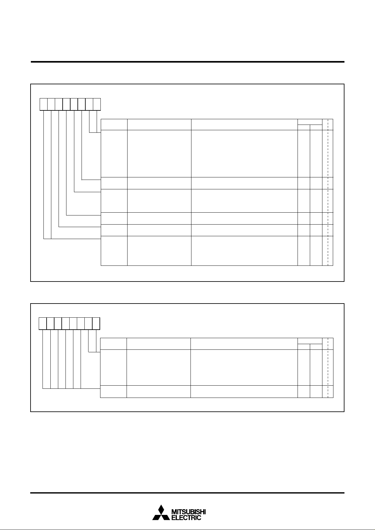
(3) Endpoint 02
MITSUBISHI MICROCOMPUTERS
38K0 Group
SINGLE-CHIP 8-BIT CMOS MICROCOMPUTER
b7
b0
EP02 set register (EP02CFG) [address 001916]
Bit symbol
BSIZ02
[1:0]
DBLB02
SQCL02
ITMD02
DIR02
TYP02
[1:0]
Bit name
Double buffer beginning address set
bit
Buffer mode select bit
Sequence toggle bit clear bit
Interrupt toggle mode select bit
Transfer direction bit
Transfer type bite
Function
In double buffer mode set the beginning address of buff er 1
area, using a relative value for the beginning address of
buffer 0.
b1b0
0 0 = 8 bytes
0 1 = 16 bytes
1 0 = 64 bytes
1 1 = 128 bytes
0 : Single buffer mode
1 : Double buffer mode
0 : Toggle bit clear disabled
1 : Writing “1” clears the toggle bit and DATA0 is used
as the next data PID.
“0” is always read when reading.
0 : Normal mode
1 : Continuous toggle mode (v alid at Interrupt IN transf er)
0 : OUT (Data is received from the host.)
1 : IN (Data is transmitted to the host.)
b7b6
0 0 : Transfer disabled
0 1 : Bulk transfer
1 0 : Interrupt transfer
1 1 : Isochronous transfer
At reset
H/W S/W
–
0
0
0
0
0
0
–: State remaining
O
–
O
–
O
–
O
–
O
–
O
WR
O
O
O
O
O
O
Fig. 54 Structure of EP02 set register
b7
000000
b0
EP02 control register 1 (EP02CON1) [address 001A16]
Bit symbol
PID02
[1: 0]
b7:b2
Response PID bit
Not used
Fig. 55 Structure of EP02 control register 1
Bit name
Function
b1 b0
0 0 : NAK
0 1 : Automatic response (ACK, NAK, DATA0, DATA1)
1 X : STALL
At occurrence of over-max. packet size :
B1 is set to “1” by the hardware.
Write “0” when writing.
“0” is read when reading.
At reset
H/W S/W
–
0
–
–: State remaining
OOO
–
WR
O
43
Page 44

MITSUBISHI MICROCOMPUTERS
38K0 Group
SINGLE-CHIP 8-BIT CMOS MICROCOMPUTER
b7
00 00000
b0
EP02 control register 2 (EP02CON2) [address 001B16]
Bit symbol
B0VAL02
b7:b1
Buffer 0 enable bit
Not used
Fig. 56 Structure of EP02 control register 2
b7
00 00000
b0
EP02 control register 3 (EP02CON3) [address 001C16]
Bit symbol
B1VAL02
b7:b1
Buffer 1 enable bit
Not used
Bit name
Bit name
Function
When the selected endpoint is IN, writing “1” to this bit
makes the transmitting data a set state (SIE is possible
to read).
When the selected endpoint is OUT, writing “1” to this
bit makes data reception possible (SIE is possible to
write).
Write “0” when writing.
“0” is read when reading.
Function
When the selected endpoint is IN, writing “1” to this bit
makes the transmitting data a set state (SIE is possible
to read).
When the selected endpoint is OUT, writing “1” to this
bit makes data reception possible (SIE is possible to
write).
In double buffer mode this bit is valid.
Write “0” when writing.
“0” is read when reading.
At reset
H/W S/W
0
–
–: State remaining
At reset
H/W S/W
0
–
–: State remaining
OOO
–
–
OOO
–
–
WR
O
WR
O
Fig. 57 Structure of EP02 control register 3
b7
00 000
b0
EP02 interrupt source register (EP02REQ) [address 001D16]
Bit symbol
B0RDY02
B1RDY02
ERR02
b7 to b3
USB function/Endpoint 2 buffer 0
ready interrupt bit
USB function/Endpoint 2 buffer 1
ready interrupt bit
USB function/Endpoint 2 error
interrupt bit
Not used
Fig. 58 Structure of EP02 interrupt source register
Bit name
Function
0 : No interrupt request issued
1 : Interrupt request issued
This bit is set to “1” when the buffer 0 is ready state
(enabled to be read/written) on USB function/Endpoint 2.
“0” can be set by software, but “1” cannot be set.
0 : No interrupt request issued
1 : Interrupt request issued
In single buffer mode this bit is invalid.
This bit is set to “1” when the buffer 1 is ready state
(enabled to be read/written) on USB function/Endpoint 2
in double buffer mode.
“0” can be set by software, but “1” cannot be set.
0 : No interrupt request issued
1 : Interrupt request issued
This bit is set to “1” when STALL response occurs on
USB function/Endpoint 2.
“0” can be set by software, but “1” cannot be set.
Write “0” when writing.
“0” is read when reading.
At reset
H/W S/W
0
0
0
0
0
0
–
–
WR
O
O
O
O
O
O
O
O
44
Page 45

MITSUBISHI MICROCOMPUTERS
38K0 Group
SINGLE-CHIP 8-BIT CMOS MICROCOMPUTER
b7
0
b0
EP02 byte number register 0 (EP02BYT0) [address 001E16]
Bit symbol
B0BYT02
[6:0]
b7
IN : Transmit byte number bit
OUT : Receive byte number bit
Not used
Fig. 59 Structure of EP02 byte number register 0
b7
0
b0
EP02 byte number register 1 (EP02BYT1) [address 001F16]
Bit symbol
B1BYT02
[6:0]
b7
IN : Transmit byte number bit
OUT : Receive byte number bit
Not used
Bit name
Bit name
Function
Single buffer mode: Set the transmitting byte number.
Double buffer mode : Set the transmitting byte number
of buffer 0.
Single buffer mode: The received byte number is
automatically set.
Double buffer mode : The received b yte n umber of b uff er 0
is automatically set.
Write “0” when writing.
“0” is read when reading.
Function
Single buffer mode: These bits are invalid.
Double buffer mode : Set the transmitting byte number
of buffer 1.
Single buffer mode: These bits are invalid.
Double buffer mode : The received b yte n umber of b uff er 1
is automatically set.
Write “0” when writing.
“0” is read when reading.
At reset
H/W S/W
–
0
0
–
–: State remaining
At reset
H/W S/W
0
0
–
–: State remaining
O
–
O
–
O
–
O
–
O
–
O
WR
O
✕
O
WR
O
✕
O
Fig. 60 Structure of EP02 byte number register 1
b7
0
b0
EP02 MAX. packet size register (EP02MAX) [address 0FEC16]
Bit symbol
MXPS02
[6:0]
b7
Max. packet size bit
Not used
Bit name
Fig. 61 Structure of EP02 MAX. packet size register
Function
IN : These bits are invalid.
OUT : Set the maximum packet size.
Write “0” when writing.
“0” is read when reading.
At reset
H/W S/W
–
0
–
–: State remaining
OOO
–
WR
O
45
Page 46

MITSUBISHI MICROCOMPUTERS
38K0 Group
SINGLE-CHIP 8-BIT CMOS MICROCOMPUTER
b7
000
b0
EP02 buffer area set register (EP02BUF) [address 0FED16]
Bit symbol
BADD02
[4:0]
b7:b5
EP02 beginning address set bit
Not used
Fig. 62 Structure of EP02 buffer area set register
Bit name
Function
Set the beginning address of EP02’s buffer area.
(32-byte unit)
b4b3b2b1b0
0 0 0 1 0 : 0040
0 0 0 1 1 : 0060
..............
1 1 1 1 0 : 03C0
1 1 1 1 1 : 03E0
Write “0” when writing.
“0” is read when reading.
16
16
16
16
At reset
H/W S/W
–
0
–
–: State remaining
OOO
–
WR
O
46
Page 47

(4) Endpoint 03
MITSUBISHI MICROCOMPUTERS
38K0 Group
SINGLE-CHIP 8-BIT CMOS MICROCOMPUTER
b7
b0
EP03 set register (EP03CFG) [address 001916]
Bit symbol
BSIZ03
[1:0]
DBLB03
SQCL03
ITMD03
DIR03
TYP03
[1:0]
Bit name
Double buffer beginning address set
bit
Buffer mode select bit
Sequence toggle bit clear bit
Interrupt toggle mode select bit
Transfer direction bit
Transfer type bit
Function
In double buffer mode set the beginning address of buff er 1
area, using a relative value for the beginning address of
buffer 0.
b1b0
0 0 = 8 bytes
0 1 = 16 bytes
1 0 = 64 bytes
1 1 = 128 bytes
0 : Single buffer mode
1 : Double buffer mode
0 : Toggle bit clear disabled
1 : Writing “1” clears the toggle bit and DATA0 is used
as the next data PID.
“0” is always read when reading.
0 : Normal mode
1 : Continuous toggle mode (v alid at Interrupt IN transf er)
0 : OUT (Data is received from the host.)
1 : IN (Data is transmitted to the host.)
b7b6
0 0 : Transfer disabled
0 1 : Bulk transfer
1 0 : Interrupt transfer
1 1 : Isochronous transfer
At reset
H/W S/W
–
0
0
0
0
0
0
–: State remaining
O
–
O
–
O
–
O
–
O
–
O
WR
O
O
O
O
O
O
Fig. 63 Structure of EP03 set register
b7
000000
b0
EP03 control register 1 (EP03CON1) [address 001A16]
Bit symbol
PID03
[1:0]
b7:b2
Response PID bit
Not used
Fig. 64 Structure of EP03 control register 1
Bit name
Function
b1 b0
0 0 : NAK
0 1 : Automatic response (ACK, NAK, DATA0, DATA1)
1 X : STALL
At occurrence of over-max. packet size :
B1 is set to “1” by the hardware.
Write “0” when writing.
“0” is read when reading.
At reset
H/W S/W
–
0
–
–: State remaining
OOO
–
WR
O
47
Page 48

MITSUBISHI MICROCOMPUTERS
38K0 Group
SINGLE-CHIP 8-BIT CMOS MICROCOMPUTER
b7
00 00000
b0
EP03 control register 2 (EP03CON2) [address 001B16]
Bit symbol
B0VAL03
b7:b1
Buffer 0 enable bit
Not used
Fig. 65 Structure of EP03 control register 2
b7
0000000
b0
EP03 control register 3 (EP03CON3) [address 001C16]
Bit symbol
B1VAL03
b7:b1
Buffer 1 enable bit
Not used
Bit name
Bit name
Function
When the selected endpoint is IN, writing “1” to this bit
makes the transmitting data a set state (SIE is possible
to read).
When the selected endpoint is OUT, writing “1” to this
bit makes data reception possible (SIE is possible to
write).
Write “0” when writing.
“0” is read when reading.
Function
When the selected endpoint is IN, writing “1” to this bit
makes the transmitting data a set state (SIE is possible
to read).
When the selected endpoint is OUT, writing “1” to this
bit makes data reception possible (SIE is possible to
write).
In double buffer mode this bit is valid.
Write “0” when writing.
“0” is read when reading.
At reset
H/W S/W
0
–
–: State remaining
At reset
H/W S/W
0
–
–: State remaining
OOO
–
–
OOO
–
–
WR
O
WR
O
Fig. 66 Structure of EP03 control register 3
b7
00000
b0
EP03 interrupt source register (EP03REQ) [address 001D16]
Bit symbol
B0RDY03
B1RDY03
ERR03
b7:b3
USB function/Endpoint 3 buffer 0
ready interrupt bit
USB function/Endpoint 3 buffer 1
ready interrupt bit
USB function/Endpoint 3 error
interrupt bit
Not used
Fig. 67 Structure of EP03 interrupt source register
Bit name
Function
0 : No interrupt request issued
1 : Interrupt request issued
This bit is set to “1” when the buffer 0 is ready state
(enabled to be read/written) on USB function/Endpoint 3.
“0” can be set by software, but “1” cannot be set.
0 : No interrupt request issued
1 : Interrupt request issued
In single buffer mode this bit is invalid.
This bit is set to “1” when the buffer 1 is ready state
(enabled to be read/written) on USB function/Endpoint 3
in double buffer mode.
“0” can be set by software, but “1” cannot be set.
0 : No interrupt request issued
1 : Interrupt request issued
This bit is set to “1” when STALL response occurs on
USB function/Endpoint 3.
“0” can be set by software, but “1” cannot be set.
Write “0” when writing.
“0” is read when reading.
At reset
H/W S/W
0
0
0
0
0
0
–
–
WR
O
O
O
O
O
O
O
O
48
Page 49

MITSUBISHI MICROCOMPUTERS
38K0 Group
SINGLE-CHIP 8-BIT CMOS MICROCOMPUTER
b7
0
b0
EP03 byte number register 0 (EP03BYT0) [address 001E16]
Bit symbol
B0BYT03
[6:0]
b7
IN : Transmit byte number bit
OUT : Receive byte number bit
Not used
Fig. 68 Structure of EP03 byte number register 0
b7
0
b0
EP03 byte number register 1 (EP03BYT1) [address 001F16]
Bit symbol
B1BYT03
[6:0]
b7
IN : Transmit byte number bit
OUT : Receive byte number bit
Not used
Bit name
Bit name
Function
Single buffer mode: Set the transmitting byte number.
Double buffer mode : Set the transmitting byte number
of buffer 0.
Single buffer mode: The received byte number is
automatically set.
Double buffer mode : The received b yte n umber of b uff er 0
is automatically set.
Write “0” when writing.
“0” is read when reading.
Function
Single buffer mode: These bits are invalid.
Double buffer mode : Set the transmitting byte number
of buffer 1.
Single buffer mode: These bits are invalid.
Double buffer mode : The received b yte n umber of b uff er 1
is automatically set.
Write “0” when writing.
“0” is read when reading.
At reset
H/W S/W
–
0
0
–
–: State remaining
At reset
H/W S/W
0
0
–
–: State remaining
O
–
O
–
O
–
O
–
O
–
O
WR
O
✕
O
WR
O
✕
O
Fig. 69 Structure of EP03 byte number register 1
b7
0
b0
EP03 MAX. packet size register (EP03MAX) [address 0FEC16]
Bit symbol
MXPS03
[6:0]
b7
Max. packet size bit
Not used
Bit name
Fig. 70 Structure of EP03 MAX. packet size register
Function
IN : These bits are invalid.
OUT : Set the maximum packet size.
Write “0” when writing.
“0” is read when reading.
At reset
H/W S/W
–
0
–
–: State remaining
OOO
–
WR
O
49
Page 50

MITSUBISHI MICROCOMPUTERS
38K0 Group
SINGLE-CHIP 8-BIT CMOS MICROCOMPUTER
b7
000
b0
EP03 buffer area set register (EP03BUF) [address 0FED16]
Bit symbol
BADD03
[4:0]
b7:b5
EP03 beginning address set bit
Not used
Fig. 71 Structure of EP03 buffer area set register
Bit name
Function
Set the beginning address of EP03’s buffer area.
(32-byte unit)
b4b3b2b1b0
0 0 0 1 0 : 0040
0 0 0 1 1 : 0060
..............
1 1 1 1 0 : 03C0
1 1 1 1 1 : 03E0
Write “0” when writing.
“0” is read when reading.
16
16
16
16
At reset
H/W S/W
–
0
–
–: State remaining
OOO
–
WR
O
50
Page 51

MITSUBISHI MICROCOMPUTERS
38K0 Group
SINGLE-CHIP 8-BIT CMOS MICROCOMPUTER
EXTERNAL BUS INTERFACE (EXB)
The external bus interface (EXB) controls the data transfer between the external MCU and the 38K0 group’s CPU or its
38K0 group
CPU
CPU channel
[Interrupt type]
External bus interface
(EXB)
Memory channel
External MCU
[Direct RAM access type]
Fig. 72 External bus interface
●CPU channel
It is a data transfer course by the interrupt processing between the
external MCU and the 38K0 group’s CPU.
●Memory channel
It is a data transfer course by direct RAM access of the memory
channel controller between the external MCU and the 38K0
group’s memory (multichannel RAM)
memory (multichannel RAM). The external bus interface is shown
below.
Program ROM
Peripheral functions
USBMultichannel RAM
(USB host)
●Data transfer of memory channel
When the burst mode is selected with the burst bit of the memory
channel operation mode register, data transfer can be carried out
at the highest speed. After the external bus interface detects a rise
of external read signal/write signal and synchronizes it with the internal clock φ, it completes the data transfer between the transmit/
receive buffer and the multichannel RAM in two clocks.
However, the waiting time of two clocks at a maximum is generated to access the multichannel RAM in USB being operating
because the USB has priority to access.
Therefore, it is necessary to set up the access interval which fills
the following timing with the external MCU bus side.
In φ = 8 MHz, data transfer at about 2 Mbytes/second is possible
at a maximum. When there is access simultaneously from the
USB, it is about 1.3 Mbytes/second.
In φ = 6 MHz, data transfer at about 1.5 Mbytes/second is possible
at a maximum. When there is access simultaneously from the
USB, it is about 1 Mbytes/second.
USB bus
Address
CS, RD, WR,
DMA acknowledge
Fig. 73 Data transfer timing of memory channel
Access cycle time from externals:
•3 clocks or more of φ + Signal delay time + Data setup
time of external MCU in USB inactive
•5 clocks or more of φ + Signal delay time + Data setup
time of external MCU in USB active
51
Page 52

EXB Pin Assignment
The external bus interface (EXB) pins are shown bellow.
The 38K0 group can transmit/receive a data to/from an external
MCU, using the following signals:
•Control input signal ................ 4 (ExCS, ExA0, ExRD, ExWR)
•Data input/output pin .............. 8 (DQ0 to DQ7)
•Interrupt output signal ............ 1 (ExINT)
Additionally, the DMA interface signal and the buffer status read
select signal of 38K0 group can be set up per one by the program.
•Control input signal ................ 3 (ExTC, ExDACK, ExRD, ExA1)
•Interrupt output signal ............ 1 (ExDREQ)
MITSUBISHI MICROCOMPUTERS
38K0 Group
SINGLE-CHIP 8-BIT CMOS MICROCOMPUTER
External bus interface
External pins
External chip select
External address
External read
External write
External data
External interrupt
DMA request
Terminal count
DMA acknowledge
Status read select
: Functions as normal ports
just after reset.
Fig. 74 External bus interface (EXB) pin assignment
P34/ExCS [“L”]
7
/ExA0 [address]
P3
6
/ExRD [“L”]
P3
5
/ExWR [“L”]
P3
0
/DQ0/AN0–P17/DQ7/AN7 [data]
P1
8
3
/ExINT [“L”]
P3
0
/ExDREQ/RxD [“L”]
P4
2
/ExTC/S
P4
P4
P4
CLK
1
/ExDACK/TxD [“L”]
3
/ExA1/S
RDY
(EXB)
[“L”]
[“H”]
38K0 group
CPU
Multichannel RAM
52
Page 53

EXB Block Diagram
The block diagram of external bus interface (EXB) is shown below.
The external bus interface (EXB) consists of:
(1) External I/O interface part
(2) CPU interface part
(3) Internal memory interface part
(4) Transmit/Receive data buffer part
MITSUBISHI MICROCOMPUTERS
38K0 Group
SINGLE-CHIP 8-BIT CMOS MICROCOMPUTER
External I/O interface CPU interface
External MCU bus
P34/ExCS CPU channel
P37/ExA0
6
/ExRD
P3
5
/ExWR
P3
Command decoderOutput selector
P41/ExDACK/TxD
P42/ExTC/S
P43/ExA1/S
P40/ExDREQ/RxD
P10/DQ0/AN0–
P1
P3
3
/ExINT
7
/DQ7/AN
CLK
RDY
stt_sel Buf_WR
ExOE
7
Configuration
signal
Cch_WR
Cch_RD
TxB_RDY
RxB_RDY
Mch_RD
Mch_WR
Mch_TC
mRX_enb
mTX_enb
Mch_req
FIFO_stt
Memory channel
Transmit/Receive data
External I/O
configuration
register
controller
control
Memory channel
Internal memory
interface
Memory channel
operation mode register
Memory address
counter
End address register
Memory channel
controller
Memory channel
transmit buffer control
buffer
Transmit buffer register
status
MRDsel
Index register
EXB interrupt
source enable register
Decoder data selector
Memory address
Request acknowledge
Memory read data
Multichannel RAM
: Functions as normal ports just after reset.
Fig. 75 Block diagram of external bus interface (EXB)
Receive buffer register
Memory write data
53
Page 54

MITSUBISHI MICROCOMPUTERS
38K0 Group
SINGLE-CHIP 8-BIT CMOS MICROCOMPUTER
(1) External I/O Interface Part
The external I/O interface part consists of a command decoder
and an output selector. A command decoder generates the following signals to each unit.
●CPU interface part
•CPU channel read (Cch_RD)
•CPU channel write (Cch_WR)
●Internal memory interface part
•Memory channel read (Mch_RD)
•Memory channel write (Mch_WR)
•Memory channel terminal count (Mch_TC)
●Transmit/receive data buffer part
•Buffer write (Buf_WR)
●External I/O interface part
•Status selection (stt_sel)
•Output enable (ExOE)
Access to the CPU channel can be controlled only by setup of
external signals.
Access to the memory channel can be controlled by the value of
the external I/O configuration register and the state (mRX_enb,
mTX_enb signals) of the internal memory interface part.
The output selector has the function which selects from the state
of CPU channel (TxB_RDY and RxD_RDY) and the state of
memory channel (Mch_req) as the signal assigned to P33/
ExINT pin and P40/ExDREQ/RxD pin.
(2) CPU Interface Part
The CPU interface part consists of the decoder/data selector of
the CPU channel, the CPU write register and CPU channel controller
●Decoder/data selector of CPU channel
A write operation to the CPU register is performed by generating a
write signal for each register with an address decode signal and a
write signal.
A read operation from the CPU register is performed by generating an output enable signal of the internal data bus with an module
select signal and a read signal and generating a select signal for
each register with an address decode signal.
●CPU write register
There are three CPU write registers as follows:
•EXB interrupt source enable register
•Index register
•External I/O configuration register
The EXB interrupt source register is a read-only register.
A status signal of the CPU channel controller and a status signal
of the memory channel controller in the internal memory interface
part are generated.
●CPU channel controller
The CPU channel controller generates the following signals, using
bits 0 and 1 (RXB_ENB, TXB_ENB) of EXB interrupt source enable register.
•Memory channel transmitting buffer control signal (MRD_sel),
generated in the internal memory interface part
•CPU channel command signal (Cch_RD, Cch_WR), generated
in the external I/O interface part
•Signals RxB_RDY/RxB_full and TxB_RDY/TxB_empty, generated with read/write signals from the CPU channel
54
Page 55

MITSUBISHI MICROCOMPUTERS
38K0 Group
SINGLE-CHIP 8-BIT CMOS MICROCOMPUTER
(3) Internal Memory Interface Part
The internal memory interface part consists of the CPU register
and the memory channel controller.
●CPU register
The CPU register consists of the follows:
•Memory channel operation mode register
•Memory address counter
•End address register
The CPU can set the beginning address into the memory address
counter when the memory channel operation enable bit
(MC_ENB) of EXB interrupt source enable register is “0”. When
this bit is “1”, the write operation from the CPU is invalid and each
access from the external bus causes count-up operation.
●Memory channel controller
The CPU register consists of the follows:
•Main sequencer
•Internal memory request signal generating circuit
•External memory channel request signal generating circuit
•Address end detection circuit
•Terminal end input processing circuit
(4) Transmit/Receive Data Buffer Part
The transmit/receive data buffer part consists of the 8-bit transmit
buffer register (TXBUF) and the 8-bit receive buffer register
(RXBUF).
Both CPU channel and memory channel use the same transmit
buffer register/receive buffer register to transfer a data to an external MCU bus.
(5) External Pin
The external bus interface has the following pins to connect with
an external MCU bus.
•Chip sele c t ........................... P34/ExCS
•Address................................ P37/ExA0
•Data...................................... P10/DQ0/AN0 to P17/DQ7/AN7
•Read .................................... P36/ExRD
•Write..................................... P35/ExWR
•Interrupt request .................. P33/ExINT
It also has the following pins to connect with an external DMAC.
Each pin can be programmed for an ordinary port function or a
DMA interface pin function.
•DMA request ........................ P40/ExDREQ/RxD
•DMA acknowledgment......... P41/ExDACK/TxD
•Terminal count ..................... P42/ExTC/SCLK
It also has the status read select pin (P43/ExA1/SRDY pin) to confirm a ready status of the data buffer from an external MCU bus
This pin functions as a port just after reset. The status read select
function can be set by a program.
•Status read select................ P43/ExA1/SRDY
●CPU channel: Communication with 38K0 group CPU
When a read/write operation is performed from an external MCU
bus in address signal ExA0 = “H”, the interrupt is generated and
the 38K0 group CPU can confirm its access. The 38K0 group CPU
judges the interrupt source and it starts a data transmission/reception with an external MCU bus.
●Memory channel: Communication with 38K2 group memory
multichannel RAM
When a read/write operation is performed from an external MCU
bus in address signal ExA0 = “L”, access to the multichannel RAM
is performed. Then an address of the multichannel RAM is made
by the external bus interface and it is increased at each access
completion. Consequently, FIFO access is performed.
Even if a read/write operation is performed in DACK = “L” instead
of ExCS = “L” and ExA0 = “L”, FIFO access to the multichannel
RAM is performed.
The beginning address and the end address must be set by the
CPU in advance.
55
Page 56

MITSUBISHI MICROCOMPUTERS
38K0 Group
SINGLE-CHIP 8-BIT CMOS MICROCOMPUTER
●P33/ExINT pin
Any one of the following signals for this pin can be selected:
•TxB_RDY (transmit buffer ready) output
•RxB_RDY (receive buffer ready) output
•Mch_req (memory channel request) output
Either TxB_RDY or RxB_RDY is normally selected. The memory
channel request is for an access request signal to the memory
channel.
In a small system, a data transfer processing to the internal
memory is performed in the interrupt routine. According to that
situation, the 38K0 group has the function automatically to switch
an interrupt factor attached on the interrupt pin by program.
●P4
0/ExDREQ/RxD pin
This pin is a port at the initial state. Which signal can be set by
program.
•RxB_RDY (receive buffer ready) output
•Mch_req (memory channel request) output
Mch_req of DMAC is normally selected. The output method of the
memory channel request signal depends on the burst bit (BURST)
of memory channel operation mode register. When the burst bit is
“0”, this signal is periodically output at each 1-byte transfer. (See
Figures 87 and 90.)
When the burst bit is “1”, this signal is continuously output while
the memory address counter is counting from the beginning address to the end address (See Figures 88 and 91.)
2/ExTC/SCLK pin
●P4
This pin is a port at the initial state. The terminal count signal can
be set by program.
If the terminal count signal is set at one bus cycle while a memory
channel operation write is being performed, the 38K0 group confirms that its bus cycle is the write cycle of the last data and sets
the memory channel status bits to “11
ated and the memory channel operation ends even if the memory
address counter has not reached the end address.
The CPU can obtain the last address where the data is written by
reading out the value of memory address counter. (See Figures 87
and 88.)
2”, and the interrupt is gener-
●P41/ExDACK/TxD pin
This pin is a port at the initial state. The DMA acknowledge signal
can be set by program.
The DMA acknowledge signal DACK = “L” is the same state as
that of CS = “L” and A0 = “L”. Access to multichannel RAM is
started by a rise of read signal or write signal which is set during
this term.
Note: If the DMA acknowledge signal and the chip select signal
are simultaneously active (DACK = “L” and CS = “L”), also
set the address signal A0 to “L”. If A0 is “H”, the memory
channel and the CPU channel are activated simultaneously
and it might cause some error.
56
Page 57

EXB Register List
Index
bit7 bit6 bit5 bit4 bit3 bit2 bit1 bit0
00
16
low
low
A1_CTR INT_CTR[2:0] EXB_CTR
high
high
TC_CTR DAK_CTR[1:0] DRQ_CTR[1:0]
01
16
low
At CPU read : RXBUF[7:0]
At CPU write : TXBUF[7:0]
high
02
16
low BURST MC_DIR[1:0]
high
03
16
low IM_A[7:0]
high
00000
IM_A[10:8]
04
16
low END_A[7:0]
high
00000
END_A[10:8]
External I/O configuration register
Transmit/Receive
buffer register
Memory channel operation mode register
Memory address
counter
End address
register
EXB SFR
Register Name
SYMBOL
EXBCFGL
EXBCFGH
RXBUF/TXBUF
MCHMOD
—
—
MEMADL
MEMADH
ENDADL
ENDADH
0 : “0” fixed
: Not used
The EXB register list is shown below.
MITSUBISHI MICROCOMPUTERS
38K0 Group
SINGLE-CHIP 8-BIT CMOS MICROCOMPUTER
Address
EXB interrupt source enable register
16
0030
EXB interrupt source register
0031
16
EXB index register
0033
16
Register window 1 (low)
0034
16
Register window 2 (high)
0035
16
Register Name
SYMBOL
EXBICON
EXBIREQ
EXBINDEX
EXBREG1
EXBREG2
bit7 bit6 bit5 bit4 bit3
00000
Fig. 76 EXB related registers (1)
•EXB interrupt source enable register
This register enables/disables access from an external bus and an
internal interrupt.
•EXB interrupt source register
This register indicates the state of CPU channel’s transmit/receive
buffer register and the memory channel. The same value can be
read out from the external MCU bus by using the buffer status
read select signal (A1 pin = “H”).
EXB SFR
LOW_WIN[7:0]
HIGH_WIN[7:0]
bit2 bit1 bit0
MC_ENB
MC_STS[1:0]
TXB_ENB RXB_EMB
TXB_EMPTY
INDEX[2:0]
RXB_FULL
: Not used
0 : “0” fixed
•EXB index register/Register windows 1, 2
The accessible register is switched by treating addresses 003416
and 003516 as a register window depending on the value of EXB
index register at address 003316.
Fig. 77 EXB related registers (2)
•External I/O configuration register
This register selects the function of each pin.
•Transmit/Receive buffer register
This register consists of the receive buffer register (RXBUF) and
the transmit buffer register (TXBUF)
•Memory channel operation mode register
This register sets the operation mode of the memory channel.
•Memory address counter
This is a counter to set the beginning address which FIFO accesses. This register is increased by access from the external
MCU bus.
•End address register
This register is to set the end address which FIFO accesses.
57
Page 58
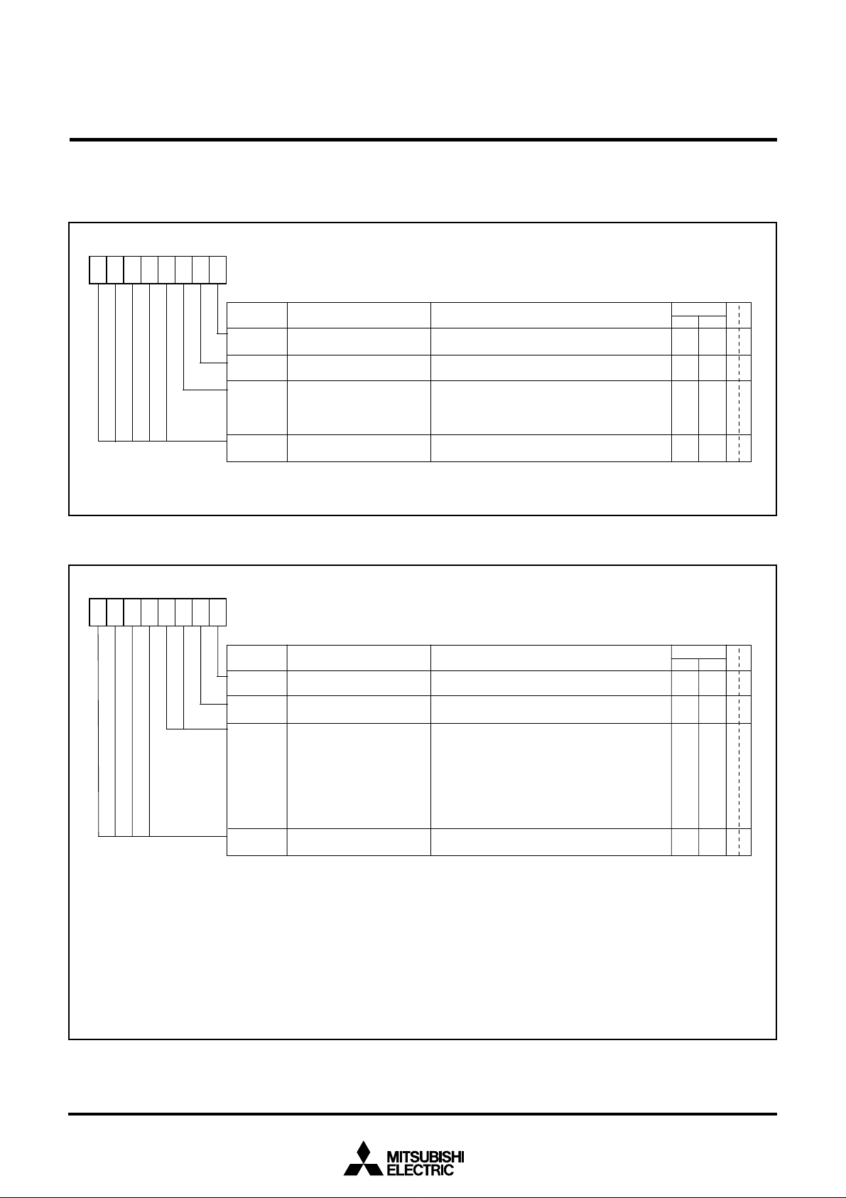
EXB Related Registers
The EXB related registers are shown below.
MITSUBISHI MICROCOMPUTERS
38K0 Group
SINGLE-CHIP 8-BIT CMOS MICROCOMPUTER
b7
00000
b0
EXB interrupt source enable register (EXBICON) [address 003016]
(Note)
Bit symbol
RXB_ENB
TXB_ENB
MC_ENB
b7:b3
Note: Do not set each bit simultaneously.
CPU channel receive enable bit
CPU channel transmit enable bit
Memory channel operation
enable bit
Not used
Bit name
Fig. 78 Structure of EXB interrupt source enable register
b7
0000
b0
EXB interrupt source register (EXBIREQ) [address 003116] (Note 1)
Bit symbol
RXB_FULL
TXB_EMPTY
MC_STS
[1:0]
(Note 2)
b7:b4
Notes 1: When the the ExA1 pin control bit of external I/O configuration register is “1”, the external MCU bus can read this
Receive buffer full bit
Transmit buffer empty bit
Memory channel status bits
Not used
register contents by setting the ExA1 pin to “H”.
2: The memory channel status bits indicate the status of memory channel. In MC_ENB = “0” these bits are always
2
”. When the memory channel operation ends, these bits are set to “112” and the memory channel operation
“00
end interrupt is generated.
These bits can be read out during operation, so that it will show that whether the external MCU bus is accessing
or not.
3: This bit is cleared to “0” when reading the transmit/receive buffer register in the CPU channel receive enable bit =
“1” or when the CPU channel receive enable bit is “0”.
4: This bit is cleared to “0” when writing to the transmit/receive buffer register in the CPU channel transmit enable bit
= “1” or when the CPU channel transmit enable bit is “0”.
Bit name
Function
0 : Operation disabled (Interrupt disabled)
1 :
Operation enabled (Receive buff er full interrupt enabled)
0 : Operation disabled (Interrupt disabled)
1 :
Operation enabled (Transmit buffer empty interrupt enabled)
0 : Operation disabled (Memory channel operation end
interrupt disabled)
1 : Operation enabled (Memory channel operation end
interrupt disabled)
Write “0” when writing.
“0” is read when reading.
Function
0 : Receive buffer empty
1 : Receive buffer full
0 : Transmit buffer full
1 : Transmit buffer empty
b3b2
0 0 : Memory channel operation stopped
0 1 : Memory channel being operating;
No external access
1 0 : Memory channel being operating;
External accessing
1 1 : Memory channel operation end; Memory
channel operation end interrupt generated
Write “0” when writing.
“0” is read when reading.
At reset
H/W S/W
–
0
0
0
–
–: State remaining
At reset
H/W S/W
0
0
0
–
–: State remaining
–
–
–
0
(Note 3)
0
(Note 4)
0
–
O
O
O
O
O
O
O
O
WR
O
O
O
O
WR
–
–
–
O
Fig. 79 Structure of EXB interrupt source register
58
Page 59
MITSUBISHI MICROCOMPUTERS
38K0 Group
SINGLE-CHIP 8-BIT CMOS MICROCOMPUTER
b7
00000
b0
EXB index register (EXBINDEX) [address 003316]
Bit symbol
INDEX
[2:0]
b7:b3
Fig. 80 Structure of EXB index register
b7
b0
Register window 1 (EXBREG1) [address 003416]
Index bits
Not used
Bit name
Function
The accessible register, using the register window,
depends on these index bits contents as follows:
b2b1b0
0 0 0 : External I/O configuration register
0 0 1 : Transmit/Receive buffer register
0 1 0 : Memory channel operation mode register
0 1 1 : Memory address counter
1 0 0 : End address register
1 0 1 : Do not set.
1 1 0 : Do not set.
1 1 1 : Do not set.
Write “0” when writing.
“0” is read when reading.
At reset
H/W S/W
–
0
–
OOO
–
–: State remaining
WR
O
Bit symbol
LOW_WIN
[7:0]
Fig. 81 Structure of Register window 1
b7
b0
Register window 2 (EXBREG2) [address 003516]
Bit symbol
HIGH_WIN
[7:0]
Bit name
–
The accessible register, using this register window,
Function
depends on the EXB index register contents as
At reset
H/W S/W
In-
definite
In-
definite
WR
OO
follows:
Index value
16” : External I/O configuration register
“00
“01
16” : Transmit/Receive buffer register
“02
16” : Memory channel operation mode register
“03
16” : Memory address counter
“04
16” : End address register
Bit name
–
The accessible register, using this register window,
Function
depends on the EXB index register contents as
At reset
H/W S/W
In-
definite
In-
definite
WR
OO
follows:
Index value
16” : External I/O configuration register
“00
“01
16” : Transmit/Receive buffer register
16” : Memory channel operation mode register
“02
16” : Memory address counter
“03
16” : End address register
“04
Fig. 82 Structure of Register window 2
59
Page 60
MITSUBISHI MICROCOMPUTERS
38K0 Group
SINGLE-CHIP 8-BIT CMOS MICROCOMPUTER
b7
000
b0
Index = 0016 : External I/O configuration register (EXBCFGL) [address 003416]
Bit symbol
EXB_CTR
INT_CTR
[2:0]
A1_CTR
b7:b5
EXB pin control bit
(Pins P1
P3
P4
Not used
Bit name
0
to P17, P30 to P34)
3
/ExINT pin control bit
3
/ExA1 pin control bit
0 : Port
1 : EXB function pin
Selects a signal of P3
ON/OFF is programmed by each bit. An output logical
sum of P3
is output as an “L” active signal.
b3b2b1
0 0 1 : RxB_RDY (RxBuf ready) output
0 1 0 : TxB_RDY (TxBuf ready) output
1 0 0 : Mch_req (Memory channel request) output
Others : Do not set.
0 : Port
1 : A1 input (used to read status)
Write “0” when writing.
“0” is read when reading.
Fig. 83 Index00[low]; Structure of External I/O configuration register
b7
000
b0
Index = 0016 : External I/O configuration register (EXBCFGH) [address 003516]
Function
3
/ExINT pin.
3
/ExINT pins set for ON are performed and it
At reset
H/W S/W
0
–
O
0
–
O
0
–
O
–
–
O
–: State remaining
WR
O
O
O
O
Bit symbol
DRQ_CTR
[1:0]
DAK_CTR
[1:0]
TC_CTR
b7:b5
P4
bit
P4
bit
P4
Not used
Bit name
0
/ExDREQ/RxD pin control
1
/ExDACK/TxD pin control
2
/ExTC/S
CLK
pin control bit
b1b0
0 0 : Port
0 1 : Do not set.
1 0 : ExDREQ function; RxB_RDY (RxBuf ready) output
1 1 : ExDREQ function; Mch_req (Memory channel
Specifies P4
Selects which mode; requiring read or write signal, or
not requiring it for use of DMA acknowledge function.
b3b2
0 0 : Port
0 1 : Do not set.
1 0 : ExDACK function; DMA acknowledge input
1 1 :ExDACK function; DMA acknowledge input
0 : Port
1 : ExTC (terminal count) input
Write “0” when writing.
“0” is read when reading.
Fig. 84 Index00[high]; Structure of External I/O configuration register
Function
request) output
1
/ExDACK/TxD pin function.
(Mode for read and write signals used together)
(Mode for read and write signals not required)
At reset
H/W S/W
0
–
O
0
–
O
0
–
O
–
–
O
–: State remaining
WR
O
O
O
O
60
Page 61
MITSUBISHI MICROCOMPUTERS
38K0 Group
SINGLE-CHIP 8-BIT CMOS MICROCOMPUTER
b7
b0
Index =0116 : Transmit/Receive buffer register (RXBUF/TXBUF) [address 003416]
Bit symbol
–RXBUF/
TXBUF
The receive buffer register (RXBUF) contents can be read out by reading to this address with the CPU. The data which the
CPU has written to this address is stored in the transmit buffer register (TXBUF).
However, do not perform wr ite operation with the CPU to this address if the memory channel direction control bits of
memory channel operation mode register is “10
source register are “01
Bit name
2
” or “102” (memory channel being operating).
Fig. 85 Index01[low]; Structure of Transmit/Receive buffer register
b7
00000
b0
Index =0216 : Memory channel operation mode register (MCHMOD) [address 003416]
Bit symbol
MC_DIR
[1:0]
BURST
b7:b3
Memory channel direction
control bit
Burst bit
Not used
Bit name
Function
The data received from an external bus is written here
at the rise timing of external write signal.
The data transmitted to an external bus is written here
at the timing of internal CPU write or memory write.
2
” (transmit mode) and the memory channel status bits of EXB interrupt
Function
b1b0
0 0 : Operation disabled
0 1 : Receive mode
1 0 : Transmit mode
1 1 : Do not set.
0 : Cycle mode (each byte transfer according to
assertion or negation)
1 : Burst mode (continuous transfer till the terminal
count)
Write “0” when writing.
“0” is read when reading.
At reset
H/W S/W
At reset
H/W S/W
0
0
–
–: State remaining
OO
–0
–
O
–
O
–
O
WR
WR
O
O
O
Fig. 86 Index02[low]; Structure of Memory channel operation mode register
b7
b0
Index = 0316 : Memory address counter (MEMADL) [address 003416]
Bit symbol
IM_A
[7:0]
–
Bit name
Register to set the low-order address of memory
channel operation beginning.
This contents are increased each time one memory
access ends.
Fig. 87 Index03[low]; Structure of Memory address counter
Function
At reset
H/W S/W
–0
WR
OO
61
Page 62
MITSUBISHI MICROCOMPUTERS
38K0 Group
SINGLE-CHIP 8-BIT CMOS MICROCOMPUTER
b7
00000
b0
Index = 0316 : Memory address counter (MEMADH) [address 003516]
Bit symbol
IM_A
[10:8]
b7:b3
–
Not used
Bit name
Fig. 88 Index03[high]; Structure of Memory address counter
b7
b0
Index = 0416 : End address register (ENDADL) [address 003416]
Bit symbol
END_A
[7:0]
–
Bit name
Function
Register to set the high-order address of memory
channel operation start.
This contents are increased each time one memory
access ends.
Write “0” when writing.
“0” is read when reading.
Function
Register to set the low-order address of memory
channel operation end.
At reset
H/W S/W
0
–
–: State remaining
At reset
H/W S/W
–: State remaining
OOO
–
–
OO
–0
WR
O
WR
Fig. 89 Index04[low]; Structure of End address register
b7
00000
b0
Index = 0416 : End address register (ENDADH) [address 003516]
Bit symbol
END_A
[10:8]
b7:b3
–
Not used
Bit name
Fig. 90 Index04[high]; Structure of End address register
Function
Register to set the high-order address of memory
channel operation end.
Write “0” when writing.
“0” is read when reading.
At reset
H/W S/W
0
–
–: State remaining
OOO
–
–
WR
O
62
Page 63
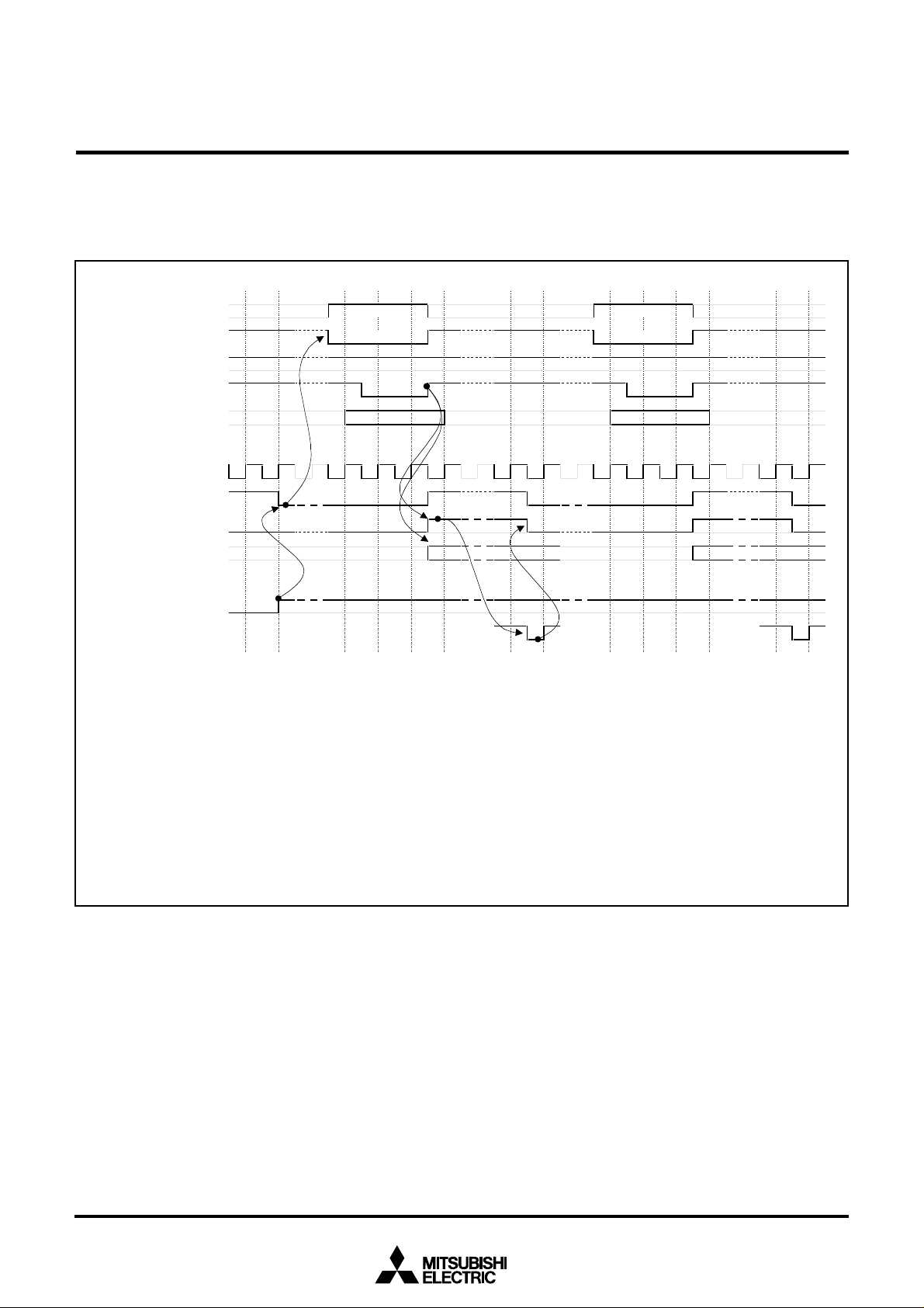
EXB Operation Timing Diagram
(1) CPU Channel Receiving Operation
CPU channel receiving operation is shown bellow.
➀➁➂
MITSUBISHI MICROCOMPUTERS
38K0 Group
SINGLE-CHIP 8-BIT CMOS MICROCOMPUTER
Address ExA0
Chip select ExCS
Read ExRD
A0 = “1”
CS = “0”
A0 = “1”
CS = “0”
➁
Write ExWR
Data DQ
0 to DQ7
Internal clock φ
Interrupt request ExINT
Receive buffer full bit RXB_FULL
CPU channel receive enable bit
[RxB_RDY]
Receive buffer RXBUF #0 #1
Transmit buffer TXBUF
RXB_ENB
Receive buffer read
RxB_RDY RxB_RDY
➀
#0 #1
➂
<Initial setting>
External I/O configuration register INT_CTR[3:1] (P3
<Operation start>
EXB interrupt source enable register RXB_ENB (CPU channel receive enable) = “1” (Receive buffer full interrupt enabled)
➀
Writing the command for enabling operation makes RXB_RDY assertion and the P33/ExINT pin goes to “L”.
If the CPU channel receive enable bit (RXB_ENB) is “0”, both the receive buffer full bit (RXB_FULL) and the receive buffer ready signal (RxB_RDY) to an
external are inactive.
➁
When a write operation is performed from an external MCU bus in the condition of ExCS = “L” and WxA0 = “H”, it will result in as follows:
• The data is written into the receive buffer (RXBUF)
• Negation of the receive buffer ready signal (RxB_RDY) to an external is made
• The RXB_FULL interrupt is generated.
➂
When the CPU reads out the receive buffer (RXBUF) with an interrupt processing program, the receive buffer full bit (RXB_FULL) is cleared to “0”.
3/ExINT pin control) = 0012 (RxB_RDY interrupt)
Fig. 91 CPU channel receiving operation
63
Page 64

(2) CPU Channel Transmitting Operation
CPU channel transmitting operation is shown bellow.
MITSUBISHI MICROCOMPUTERS
38K0 Group
SINGLE-CHIP 8-BIT CMOS MICROCOMPUTER
Address ExA0
Chip select ExCS
Read ExRD
Write ExWR
Data DQ
0
to DQ
Internal clock φ
Interrupt request ExINT
Transmit buffer empty bit
CPU channel transmit enable bit
[TxB_RDY]
TXB_EMPTY
Receive buffer RXBUF
Transmit buffer TXBUF
TXB_ENB
Transmit data write
➀
➁
➂
A0 = “1”
CS = “0”
➁’
A0 = “1”
CS = “0”
➂
7
TxB_RDY TxB_RDY
#0 #1
#0 #1
➀
➁
<Initial setting>
External I/O configuration register INT_CTR[3:1] (P3
<Operation start>
EXB interrupt source enable register TXB_ENB (CPU channel transmit enable) = “1” (Transmit buffer empty interrupt enabled)
➀
Writing the command for enabling operation generates TXB_EMPTY interrupt.
If the CPU channel transmit enable bit (TXB_ENB) is “0”, both the transmit buffer empty bit (TXB_EMPTY) and the transmit buffer ready signal (TxB_RDY) to
an external are inactive.
➁
When the CPU writes the data into the transmit buffer (TXBUF) with an interrupt processing program, the transmit buffer empty bit (TXB_EMPTY) is cleared
to “0” and assertion of the transmit buffer ready signal (TxB_RDY) to an external is made.
➂
When a read operation is performed from an external MCU bus in the condition of ExCS = “L” and ExA0 = “H”, it will result in as follows:
• The contents of the transmit buffer (TXBUF) is read out
• The transmit buffer empty bit (TXB_EMPTY) is set to “1”
• Negation of the transmit buffer ready signal (TxB_RDY) to an external is made.
3
/ExINT pin control) = 0102 (TxB_RDY interrupt)
➁’
Fig. 92 CPU channel tranmitting operation
64
Page 65

(3) Memory Channel Receiving Operation (1)-
Cycle Mode
Memory channel receiving operation (1) is shown bellow.
MITSUBISHI MICROCOMPUTERS
38K0 Group
SINGLE-CHIP 8-BIT CMOS MICROCOMPUTER
Address ExA0
Chip select ExCS
DMA acknowledge
ExDACK
Read ExRD
Write ExWR
0
to DQ
Data DQ
Internal clock φ
DMA request
ExDREQ
➔
mWR detection
mWR detection
➔
Receive buffer RXBUF
Operation enabled
Main sequencer
Memory channel operation
end interrupt
Internal memory access
➀
7
Mch_req Mch_req
➁➁’ ➂’➂➃
A0 = “0”
CS = “0”
#0 #1
#0 #1
A0 = “0”
CS = “0”
➀
012 3 5
req req
➄
Memory address
Counter end
Acknowledgment of
internal memory access
<Initial setting>
External I/O configuration register Set as necessary.
Memory channel operation mode register MC_DIR[1:0] (Memory channel direction control) = 01
Memory address counter (Example) 0100
End address register (Example) 010116
<Operation start command>
EXB interrupt source enable register MC_ENB (Memory channel operation enable) = “1” (Operation start)
➀
In the memory channel receive mode when the command for enabling operation is written, operation starts (main sequencer starts) and assertion of the
memory channel request which synchronized with a rise of φ is made.
➁
When the external MCU bus is in the condition of ExCS = “L” and ExA0 = “L” or a fall of ExWR is detected in the condition of ExDACK = “L”, negation of the
memory channel request which synchronized with a rise of φ is made.
➂
When a rise of ExWR is detected, an internal memory access sequence which synchronized with a rise of φ is activated and a data is written in the internal
memory within two clocks at a minimum.
➃
The memory address counter is increased simultaneously at write completion and assertion of the next memory channel request is made.
➄
When the write operation to the end address has been completed, the memory address counter is increased, but assertion of the next memory channel
request is not made and the memory channel operation end interrupt is generated.
Fig. 93 Memory channel receiving operation (1)
0100
16
Burst (burst) = “0” (Cycle mode)
0101
16
ack ack
➃
2 (Receive mode)
16
0102
16
➄
65
Page 66

(4) Memory Channel Receiving Operation (2)-
Burst Mode
Memory channel receiving operation (2) is shown bellow.
MITSUBISHI MICROCOMPUTERS
38K0 Group
SINGLE-CHIP 8-BIT CMOS MICROCOMPUTER
Address ExA0
Chip select ExCS
DMA acknowledge
ExDACK
Read ExRD
Write ExWR
Data DQ
0
to DQ
Internal clock φ
DMA request
ExDREQ
➔
mWR detection
➔
mWR detection
Receive buffer RXBUF
Operation enabled
Main sequencer
Memory channel operation
end interrupt
Internal memory access
➀
A0 = “x”
CS = “1”
Dack =
7
#0 #1 #2
Mch_req
➁
“0”
➂➃➄
A0 = “x”
CS = “1”
Dack =
➁
#0 #1 #2
➁’
“0”
➁’
A0 = “x”
CS = “1”
Dack =
“0”
➀
012 3 5
req req req
Memory address
Counter end
Burst end
Acknowledgment of
internal memory access
<Initial setting>
External I/O configuration register Set as necessary.
Memory channel operation mode register MC_DIR[1:0] (Memory channel direction control) = 01
Memory address counter (Example) 0100
End address register (Example) 0102
<Operation start command>
EXB interrupt source enable register MC_ENB (Memory channel operation enable) = “1” (Operation start)
➀
In the memory channel receive mode when the command for enabling operation is written, assertion of the memory channel request which synchronized
with a rise of φ is made.
➁
When a rise of ExWR is detected, an internal memory access sequence which synchronized with a rise of φ is activated and a data is written in the internal
memory within two clocks at a minimum.
➂
The memory address counter is increased simultaneously at the former data write completion.
➃
When the memory address counter reaches the end address, the detection circuit of external write signal (ExWR) operation is enabled and negation of the
memory channel request which synchronized with the following φ is made.
➄
When the write operation to the end address has been completed, the memory address counter is increased and the memory channel operation end
interrupt is generated.
0100
Fig. 94 Memory channel receiving operation (2)
16
Burst (burst) = “1” (Burst mode)
16
16
0101
16
ack ack ack
0102
16
0103
16
➂➃➄
2
(Receive mode)
66
Page 67

(5) Memory Channel Receiving Operation (3)-
Burst Mode (Terminal Count)
Memory channel receiving operation (3) is shown bellow.
MITSUBISHI MICROCOMPUTERS
38K0 Group
SINGLE-CHIP 8-BIT CMOS MICROCOMPUTER
Address ExA0
Chip select ExCS
DMA acknowledge
ExDACK
Terminal count ExTC
Write ExWR
0
to DQ
Data DQ
Internal clock φ
DMA request
ExDREQ
➔
mWR detection
➔
mWR detection
Receive buffer RxBuf
mTC detection
➔
TC synchronizing
TC end
Operation enabled
Main sequencer
emory channel operation
Internal memory access
end interrupt
A0 = “x”
CS = “1”
Dack =
➀’
A0 = “x”
CS = “1”
“0”
Dack =
“0”
➁’
➀’
TC
7
#0 #1
Mch_req
#0 #1
➀
➀
➁’ ➁’
012 3 (5) 5
req
➁’ ➁’
➁
➁
➁
Memory address
Counter end
Burst end
Acknowledgment of
internal memory access
<Initial setting>
External I/O configuration register Set as necessary.
Memory channel operation mode register MC_DIR[1:0] (Memory channel direction control) = 01
Memory address counter (Example) 0100
End address register (Example) 0107
<Operation start command>
EXB interrupt source enable register MC_ENB (Memory channel operation enable) = “1” (Operation start)
➀
When a rise of TC is detected, negation of the memory channel request which synchronized with a rise of φ is made.
➁
When the write operation to the end address has been completed, the memory channel operation end interrupt is generated.
Fig. 95 Memory channel receiving operation (3)
0100
16
Burst (burst) = “1” (Burst mode)
0101
16
ack ack
16
16
2
(Receive mode)
0102
16
67
Page 68

(6) Memory Channel Transmitting Operation
(1)-Cycle Mode
Memory channel transmitting operation (1) is shown bellow.
MITSUBISHI MICROCOMPUTERS
38K0 Group
SINGLE-CHIP 8-BIT CMOS MICROCOMPUTER
Address ExA0
Chip select ExCS
DMA acknowledge
ExDACK
Read ExRD
Write ExWR
0
to DQ
Data DQ
Internal clock φ
DMA request
ExDREQ
➔
mRD detection
mRD detection
➔
Transmission completed
Transmit buffer TXBUF
Operation enabled
Main sequencer
Memory channel operation
end interrupt
Internal memory access
➀
7
➀
012 34 5
➁
A0 = “x”
CS = “1”
Dack =
“0”
➂➃
#0 #1
Mch_req Mch_req
#0 #1
req req
➄
➂’➂➃
A0 = “x”
CS = “1”
Dack =
➅
“0”
➂’ ➅
Memory address
Counter end
Acknowledgment of
internal memory access
0100
16
ack ack
➁
<Initial setting>
External I/O configuration register Set as necessary.
Memory channel operation mode register MC_DIR[1:0] (Memory channel direction control) = 10
Memory address counter (Example) 0100
End address register (Example) 0101
<Operation start command>
EXB interrupt source enable register MC_ENB (Memory channel operation enable) = “1” (Operation start)
➀
In the memory channel transmit mode when the command for enabling operation is written, operation starts (main sequencer starts) and an internal
memory access sequence which synchronized with a rise of φ is activated.
➁
A data is read out from the internal memory within two clocks at a minimum and this data is stored in the transmit buffer (TXBUF). The memor y address
counter is simultaneously increased and assertion of the memory channel request is made.
➂
When the external MCU bus is in the condition of ExCS = “L” and ExA0 = “L” or a fall of ExRD is detected in the condition of ExDACK = “L”, negation of the
memory channel request which synchronized with a rise of φ is made.
➃
When a rise of ExRD is detected, an internal memory access sequence which synchronized with a rise of φ is activated.
➄
A data is read out from the internal memory within two clocks at a minimum and this data is stored in the transmit buffer (TXBUF). The memor y address
counter is simultaneously increased and assertion of the memory channel request is made.
When the read operation from the end address has been completed, the transition to the status to wait the memory channel operation end occurs.
➅
When a rise of ExRD is detected, the memory channel operation sequence ends and the memory channel operation end interrupt is generated.
Fig. 96 Memory channel tranmitting operation (1)
0101
16
Burst (burst) = “0” (Cycle mode)
16
16
➄
2
(Transmit mode)
0102
16
68
Page 69

(7) Memory Channel Transmitting Operation
(2)-Burst Mode
Memory channel transmitting operation (2) is shown bellow.
MITSUBISHI MICROCOMPUTERS
38K0 Group
SINGLE-CHIP 8-BIT CMOS MICROCOMPUTER
Address ExA0
Chip select ExCS
DMA acknowledge
ExDACK
Read ExRD
Write ExWR
0
to DQ
Data DQ
Internal clock φ
DMA request
ExDREQ
➔
mRD detection
➔
mRD detection
Transmission completed
Transmit buffer TXBUF
Operation enabled
Main sequencer
emory channel operation
end interrupt
Internal memory access
➀
7
➁➂’
A0 = “x”
CS = “1”
Dack =
Mch_req
#0 #1 #2
➂
“0”
➂
#0 #1 #2
➃➄
A0 = “x”
CS = “1”
Dack =
“0”
➂’
A0 = “x”
CS = “1”
Dack =
➅
“0”
➅
➀
012 3 4 5
req req req
Memory address
Counter end
Burst end
Acknowledgment of
internal memory access
0100
16
ack ack ack
0101
16
0102
16
0103
16
➁➃➄
<Initial setting>
External I/O configuration register Set as necessary.
Memory channel operation mode register MC_DIR[1:0] (Memory channel direction control) = 10
Memory address counter (Example) 0100
End address register (Example) 0102
<Operation start command>
EXB interrupt source enable register MC_ENB (Memory channel operation enable) = “1” (Operation start)
➀
In the memory channel transmit mode when the command for enabling operation is written, an internal memory access sequence which synchronized with
a rise of φ is activated.
➁
A data is read out from the internal memory within two clocks at a minimum and this data is stored in the transmit buffer (TXBUF). The memor y address
counter is simultaneously increased and assertion of the memory channel request is made.
➂
When a rise of ExRD is detected, an internal memory access sequence which synchronized with a rise of φ is activated.
➃
A data is read out from the internal memory within two clocks at a minimum and this data is stored in the transmit buffer (TXBUF). The memor y address
counter is simultaneously increased.
➄
When the read operation from the end address has been completed, the detection circuit of external read signal (ExRD) operation is enabled and negation
of the memory channel request which synchronized with the following φ is made.
➅
When a rise of ExRD is detected, the memory channel operation sequence ends and the memory channel operation end interrupt is generated.
Burst (burst) = “1” (Burst mode)
16
16
2
(Transmit mode)
Fig. 97 Memory channel tranmitting operation (2)
69
Page 70

MITSUBISHI MICROCOMPUTERS
O
O
O
O
38K0 Group
SINGLE-CHIP 8-BIT CMOS MICROCOMPUTER
MULTICHANNEL RAM
The 38K0 group has the built-in multichannel RAM including the
small logic circuit (RAM I/F) instead of ordinary RAM.
The multichannel RAM has the USB channel and the EXB channel
in addition to the CPU channel.
The multichannel RAM controls access from CPU, USB and EXB,
synchronizing control with φ. The USB transfer rate is about 1.5
Mbytes/second. Access to the multichannel RAM is performed at
every about 5.3 clocks in φ = 8 MHz, or at every about 4 clocks in
φ = 6 MHz. The USB’s access has priority to the EXB’s.
No wait No wait No wait
ONW = “H”
φ
CPU bus cycle
Multichannel RAM
CPU AD
RD/WR
USB REQ
EXB REQ
RAM area Except RAM RAM area
The one wait function (ONW function) of 38000 series CPU is
used internally to control access with the CPU. When receiving an
access request from the USB or the EXB, the multichannel RAM
outputs ONW signal to wait the CPU for one clock, and access of
the USB or the EXB is performed.
If the multichannel RAM is outputting ONW signal while the CPU
is in the state of reading/writing for the RAM area, the CPU read
cycle or write cycle is extended by 1 period of φ.
Except RAM No RD/WR
ONW
RAM bus cycle
RAM access right
RAM RD/WR
Fig. 98 Multichannel RAM timing diagram (no wait)
ne wait
Prior CPU
RAM area
EXB
CPU bus cycle
Multichannel RAM
RAM bus cycle
CPU accessing RAM at the latter part
φ
CPU AD
RD/WR
USB REQ
EXB REQ
ONW
RAM access right
RAM RD/WR
CPU USB CPU
ne wait
Prohibiting continuous access of
USB/EXB
Prior CPU Prior CPUPrior USB
RAM area
CPU CPU CPU EXB CPUUSB USB
USB having priority of USB/EXB
ne wait
simultaneous access
RAM area
ne wait
2-cycle wait (max.) for EXB
RAM area
Fig. 99 Multichannel RAM timing diagram (one wait)
70
Page 71

Multichannel RAM Operation Example
The multichannel RAM operation example is shown below.
This example shows the case that an external MCU uses the
38K0 group as a peripheral LSI (USB controller).
The following explains that the external MCU reads out the data
which is received via the USB.
➀ The data which is received via the USB is written into the multi-
channel RAM.
➁ Receive completion is propagated to the CPU.
➂ The external bus interface is activated owing to the CPU.
➃ (1) The external bus interface sets the data which is read from
the multichannel RAM into the internal data buffer.
(2) The external MCU reads out the data bus buffer of the exter-
nal bus interface.
(3) The above operation is repeated by the number of the re-
ceived bytes. After that, the data transfer is completed.
MITSUBISHI MICROCOMPUTERS
38K0 Group
SINGLE-CHIP 8-BIT CMOS MICROCOMPUTER
CPU
➂
Activating
External MCU bus
External MCU
External bus interface
➃
FIFO read of received data
by External bus interface
Fig. 100 Multichannel RAM operation example
Program ROM
➁
Notice of receive completion
Multichannel RAM
Peripheral functions
USB
➀
FIFO write of received data
by USB
USB bus
(USB host)
71
Page 72

MITSUBISHI MICROCOMPUTERS
A
AD
A
N
)
b
b
7
6
5
9
38K0 Group
SINGLE-CHIP 8-BIT CMOS MICROCOMPUTER
A-D CONVERTER
The functional blocks of the A-D converter are described below.
[A-D Conversion Register 1, 2 (AD1, AD2)]
16, 003816
0037
The A-D conversion register is a read-only register that stores the
result of an A-D conversion. When reading this register during an
A-D conversion, the previous conversion result is read.
Bit 7 of the A-D conversion register 2 must be set to “0”.Not only
10-bit reading but also only high-order 8-bit reading of conversion
result can be performed by selecting the reading procedure of the
A-D conversion registers 1, 2 after A-D conversion is completed
(in Figure 102).
The 8-bit reading inclined to MSB is performed when reading the
A-D converter register 1 after A-D conversion is started or reset;
and when the A-D converter register 1 is read after reading the AD converter register 2, the 8-bit reading inclined to LSB is
performed.
[A-D Control Register (ADCON)] 003616
The A-D control register controls the A-D conversion process. Bits
0 to 2 select a specific analog input pin. Bit 3 signals the completion of an A-D conversion. The value of this bit remains at “0”
during an A-D conversion, and changes to “1” when an A-D conversion ends. Writing “0” to this bit starts the A-D conversion.
Comparison Voltage Generator
The comparison voltage generator divides the voltage between
VREF and AVSS into 1024, and that outputs the comparison voltage.
The A-D converter successively compares the comparison voltage
Vref in each mode, dividing the VREF voltage (see below), with the
input voltage.
•10-bit reading
VREF
Vref = ✕ n (n = 0–1023)
1024
•8-bit reading
VREF
Vref = ✕ n (n = 0–255)
256
Channel Selector
The channel selector selects one of the input ports P17/AN7–P10/
AN0.
Comparator and Control Circuit
The comparator and control circuit compares an analog input voltage with the comparison voltage, and then stores the result in the
A-D conversion registers 1, 2. When an A-D conversion is completed, the control circuit sets the AD conversion completion bit
and the AD interrupt request bit to “1”.
Note that because the comparator consists of a capacitor coupling, set f(system clock) to 500 kHz or more during an A-D
conversion.
7
Fig. 101 Structure of A-D control register
10-bit reading
(Read address 003816 before 003716)
( a d d r e s s 0 0 3 81
(a d d r e s s 0 0 3 71
Note : Bits 2 to 7 of address 003816 become “0”
at reading.
8-bit reading
(Read only address 003716)
(address 003716)
- D c o n t r o l r e g i s t e
0
( A D C O N : a d d r e s s 0 0 3 6
n a l o g i n p u t p i n s e l e c t i o n b i t
0 0 0 : P 10/ D Q0/ A N
0 0 1 : P 11/ D Q1/ A N
0 1 0 : P 12/ D Q2/ A N
0 1 1 : P 13/ D Q3/ A N
1 0 0 : P 14/ D Q4/ A N
1 0 1 : P 15/ D Q5/ A N
1 1 0 : P 16/ D Q6/ A N
1 1 1 : P 17/ D Q7/ A N
conversion completion bit
0 : Conversion in progress
1 : Conversion completed
o t u s e d ( i n d e f i n i t e a t r e a d
( T h e s e b i t s a r e w r i t e d i s a b l e d b i t s . )
b 7
6)
6)
b7
0
b
b7
b9b8b7b6 b5 b4b3b2
r
b
b
b 4b 3b2b 1b 0
1 6
)
s
0
1
2
3
4
5
6
7
b0
b 8
b
b 0
b 0
Fig. 102 10-bit A-D mode reading
72
Page 73

D a t a b u s
MITSUBISHI MICROCOMPUTERS
38K0 Group
SINGLE-CHIP 8-BIT CMOS MICROCOMPUTER
A - D c o n t r o l r e g i s t e r
( a d d r e s s
P 10/ D Q0/ A N
P 11/ D Q1/ A N
P 12/ D Q2/ A N
P 13/ D Q3/ A N
P 14/ D Q4/ A N
P 15/ D Q5/ A N
P 16/ D Q6/ A N
P 17/ D Q7/ A N
Fig. 103 A-D converter block diagram
0 0 3 6
1 6
)
0
1
2
3
4
5
6
7
r
C
h a n n e l s e l e c t o
b 7b0
3
A - D i n t e r r u p t r e q u e s t
( a d d r e s s
( a d d r e s s
0 0 3 8
0 0 3 7
1 6
1 6
)
)
C o m p a r a t o r
A - D c o n t r o l c i r c u i t
A - D c o n v e r s i o n r e g i s t e r 2
A - D c o n v e r s i o n r e g i s t e r 1
10
Resistor ladder
V
R E F
V
S S
73
Page 74
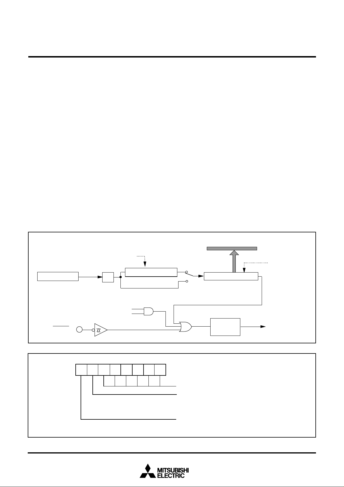
MITSUBISHI MICROCOMPUTERS
38K0 Group
SINGLE-CHIP 8-BIT CMOS MICROCOMPUTER
WATCHDOG TIMER
The watchdog timer gives a mean of returning to the reset status
when a program cannot run on a normal loop (for example, because of a software run-away). The watchdog timer consists of an
8-bit watchdog timer L and an 8-bit watchdog timer H.
Standard Operation of Watchdog Timer
When any data is not written into the watchdog timer control register (address 003916) after resetting, the watchdog timer is in the
stop state. The watchdog timer starts to count down by writing an
optional value into the watchdog timer control register (address
003916) and an internal reset occurs at an underflow of the watchdog timer H.
Accordingly, programming is usually performed so that writing to
the watchdog timer control register (address 003916) may be
started before an underflow. When the watchdog timer control register (address 003916) is read, the values of the high-order 6 bits
of the watchdog timer H, STP instruction disable bit (bit 6), and
watchdog timer H count source selection bit (bit 7) are read.
Initial Value of Watchdog Timer
At reset or writing to the watchdog timer control register (address
003916), each watchdog timer H and L is set to “FF16.”
●Watchdog timer H count source selection bit operation
Bit 7 of the watchdog timer control register (address 003916) permits selecting a watchdog timer H count source. When this bit is
set to “0”, the count source becomes the underflow signal of
watchdog timer L. The detection time is set to 131.072 ms at system clock 8 MHz frequency.
When this bit is set to “1”, the count source becomes the system
clock divided by 16. The detection time in this case is set to 512
µs at system clock 8 MHz frequency. This bit is cleared to “0” after
resetting.
●Operation of STP instruction disable bit
Bit 6 of the watchdog timer control register (address 003916) permits disabling the STP instruction when the watchdog timer is in
operation.
When this bit is “0”, the STP instruction is enabled.
When this bit is “1”, the STP instruction is disabled.
Once the STP instruction is executed, an internal reset occurs.
When this bit is set to “1”, it cannot be rewritten to “0” by program.
This bit is cleared to “0” after resetting.
“ F F
1 6
” i s s e t w h e n
w a t c h d o g t i m e r
c o n t r o l r e g i s t e r i s
w r i t t e n t o .
S y s t e m c l o c k
1 / 1 6
S T P i n s t r u c t i o n d i s a b l e b i t
S T P i n s t r u c t i o n
RESET
Fig. 104 Block diagram of Watchdog timer
b 7
W a t c h d o g t i m e r L ( 8 )
b 0
“ 0 ”
“1”
W a t c h d o g t i m e r H ( 8 )
Watchdog timer H count
source selection bit
R e s e t c i r c u i t
W a t c h d o g t i m e r c o n t r o l r e g i s t e r
( W D T C O N : a d d r e s s 0 0 3 9
Watchdog timer H (for read-out of high-order 6 bit)
STP instruction disable bit
0: STP instructi on enabled
1: STP instructi on dis abled
1 6
)
D a t a b u s
“ F F
1 6
w a t c h d o g t i m e r
c o n t r o l r e g i s t e r i s
w r i t t e n t o .
Internal reset
” i s s e t w h e n
Fig. 105 Structure of Watchdog timer control register
Watchdog timer H c ount source selectio n bit
0: Watchdog timer L underflow
1: System clock/16
74
Page 75
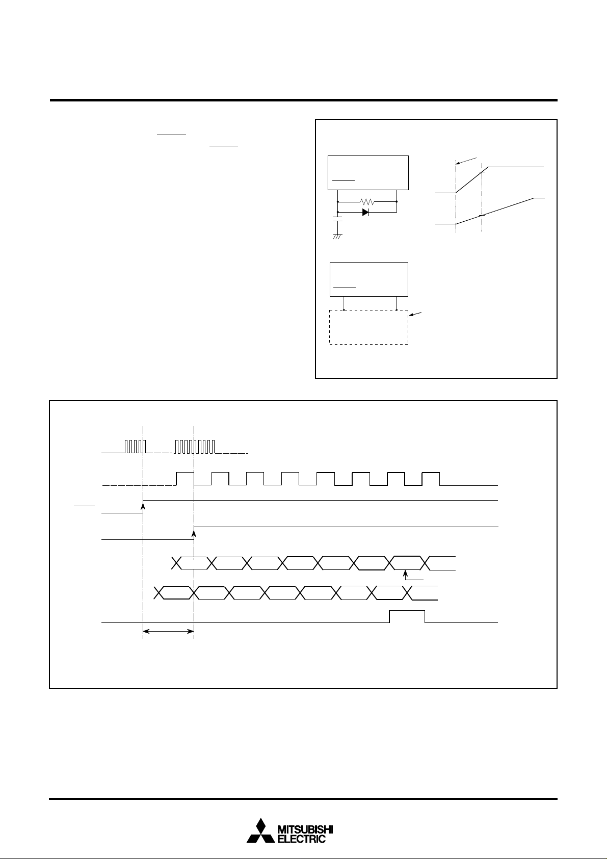
RESET CIRCUIT
To reset the microcomputer, RESET pin should be held at an “L”
level for 16 cycles or more of XIN. Then the RESET pin is returned
to an “H” level (the power source voltage should be between 3.0 V
and 5.25 V, and the oscillation should be stable), reset is released.
After the reset is completed, the program starts from the address
contained in address FFFD16 (high-order byte) and address
FFFC16 (low-order byte). Make sure that the reset input voltage is
0.6 V for VCC of 3.0 V.
MITSUBISHI MICROCOMPUTERS
38K0 Group
SINGLE-CHIP 8-BIT CMOS MICROCOMPUTER
P o w e r o n
( N o t e )
0 . 2 V
R E S E T
R E S E T
P o w e r
s o u r c e
v o l t a g e
V
C C
0 V
R e s e t i n p u t
v o l t a g e
0 V
N o t e : R e s e t r e l e a s e v o l t a g e ; V c c = 3 . 0 V
V
C C
P o w e r s o u r c e
v o l t a g e d e t e c t i o n
c i r c u i t
C C
I N
X
φ
R E S E T
I n t e r n a l
r e s e t
A d d r e s s
D a t a
S Y N C
Fig. 106 Example of reset circuit
H,L
A DH
N)
A D
R e s e t a d d r e s s f r o m t h e v e c t o r t a b l e .
• f (φ) .
?
1 0 . 5 t o 1 8 . 5 c l o c k c y c l e
XI
N:
?
?
s
N o t e s
??
??
a n d f
= 8
1 : T h e f r e q u e n c y r e l a t i o n o f f ( XI
2 : T h e q u e s t i o n m a r k s ( ? ) i n d i c a t e a n u n d e f i n e d s t a t e t h a t d e p e n d s o n t h e p r e v i o u s s t a t e .
?
? ?
F F F CF F F D
L
A D
N)
(φ) i s f ( XI
Fig. 107 Reset sequence
75
Page 76

PLL CIRCUIT (FREQUENCY SYNTHESIZER)
The PLL circuit generates fVCO (PLL output clock), which is required for fUSB (USB clock) and fSYN (fUSB division clock), from
f(XIN) (external input reference clock). Figure 108 shows the PLL
circuit block diagram.
It is possible to input 6 or 12 MHz clock from the externals as a
standard clock input. When using the USB function, set the PLL
operation mode selection bit so that fvco may be set to 48 MHz.
The PLL circuit operates by setting the PLL operation enable bit to
“1”. When supplying fVCO to the USB block, wait for the oscillation
stable time (1ms or less) of PLL before selecting fVCO with the
USB clock selection bit.
According to the setting of the USB clock division ratio selection
bit, the division clock of fUSB is supplied to fSYN. When using this
clock as system clock, set the USB clock division ratio selection
bit so that it may be set to 6 MHz, 8 MHz or 12 MHz. (However,
using it only when fUSB is 48MHz is recommended).
MITSUBISHI MICROCOMPUTERS
38K0 Group
SINGLE-CHIP 8-BIT CMOS MICROCOMPUTER
f ( X
I N
)
PLL
P L L C O N
(address 0FF816)
Fig. 108 Block diagram of PLL circuit
f
VCO
U S B C O N
(address 0010
f
USB
Division circuit
16
)
f
S Y N
76
Page 77
SINGLE-CHIP 8-BIT CMOS MICROCOMPUTER
b 0b 7
PLL control register
(PLLCON: address 0FF8
N o t u s e d ( r e t u r n “ 0” w h e n r e a d )
U S B c l o c k d i v i s i o n r a t i o s e l e c t i o n b i t s
b 4 b 3
0 0 : D i v i d e d b y 8 ( f
0 1 : D i v i d e d b y 6 ( f
1 0 : D i v i d e d b y 4 ( f
1 1 : N o t s e l e c t e d
P L L o p e r a t i o n m o d e s e l e c t i o n b i t s
b 6 b 5
0 0 : N o t m u l t i p l i e d ( f
0 1 : D o u b l e ( f
1 0 : Q u a d r u p l e ( f
1 1 : M u l t i p l i e d b y 8 ( f
P L L E n a b l e B i t
0 : D i s a b l e d
1 : E n a b l e d
V C O
= f
V C O
S Y N
S Y N
S Y N
V C O
X I N
= f
V C O
MITSUBISHI MICROCOMPUTERS
38K0 Group
16
)
= f
U S B
/ 8 )
= f
U S B
/ 6 )
= f
U S B
/ 4 )
= f
X I N
)
✕ 2 )
X I N
✕ 4 )
= f
X I N
✕ 8 )
Fig. 109 Structure of PLL control register
77
Page 78

MITSUBISHI MICROCOMPUTERS
38K0 Group
SINGLE-CHIP 8-BIT CMOS MICROCOMPUTER
CLOCK GENERATING CIRCUIT
An oscillation circuit can be formed by connecting a resonator between XIN and XOUT. Use the circuit constants in accordance with
the resonator manufacturer’s recommended values. No external
resistor is needed between XIN and XOUT since a feed-back resistor exists on-chip.
Frequency Control
Either fSYN or f(XIN) can be selected as an internal system clock.
Furthermore, the frequency of internal clock φ can be selected by
the system clock division ratio selection bit.
(1) fSYN clock
fSYN clock is generated by the PLL circuit. f(XIN) or fVCO can be
selected as an input clock. When using as an internal system
clock, there is restriction on use. Refer to the clause of “PLL CIRCUIT”.
(2) f(XIN) clock
The frequency applied to the XIN pin is used as an internal system
clock frequency.
Oscillation Control
(1) Stop mode
If the STP instruction is executed, the internal clock φ stops at an
“H” level, and the XIN oscillator stops. When the oscillation stabi-
lizing time set after STP instruction released bit is “0,” the
prescaler 12 is set to “FF16” and timer 1 is set to “0116.” When the
oscillation stabilizing time set after STP instruction released bit is
“1,” set the sufficient time for oscillation of used oscillator to stabilize since nothing is set to the prescaler 12 and timer 1. XIN
divided by 16 is compulsorily connected to the input of the
prescaler 12. Oscillator restarts when an external interrupt (including USB resume interrupt) is received, but the internal clock φ
remains at “H” until timer 1 underflows. The internal clock φ is not
supplied until timer 1 underflows. Because the sufficient time is required for the oscillation to stabilize when a ceramic resonator etc.
is used. When the oscillator is restarted by reset, apply “L” level to
the RESET pin until the oscillation is stable since a wait time will
not be generated automatically.
(2) Wait mode
If the WIT instruction is executed, the internal clock φ stops at an
“H” level, but the oscillator does not stop. The internal clock φ re-
starts at reset or when an interrupt is received. Since the oscillator
does not stop, normal operation can be started immediately after
the clock is restarted.
To ensure that the interrupts will be received to release the STP or
WIT state, their interrupt enable bits must be set to “1” before executing of the STP or WIT instruction.
When releasing the STP state, the prescaler 12 and timer 1 will
start counting the clock XIN divided by 16. Accordingly, set the
timer 1 interrupt enable bit to “0” before executing the STP instruction.
■Note
When using the oscillation stabilizing time set after STP instruction
released bit set to “1”, evaluate time to stabilize oscillation of the
used oscillator and set the value to the timer 1 and prescaler 12.
78
Page 79
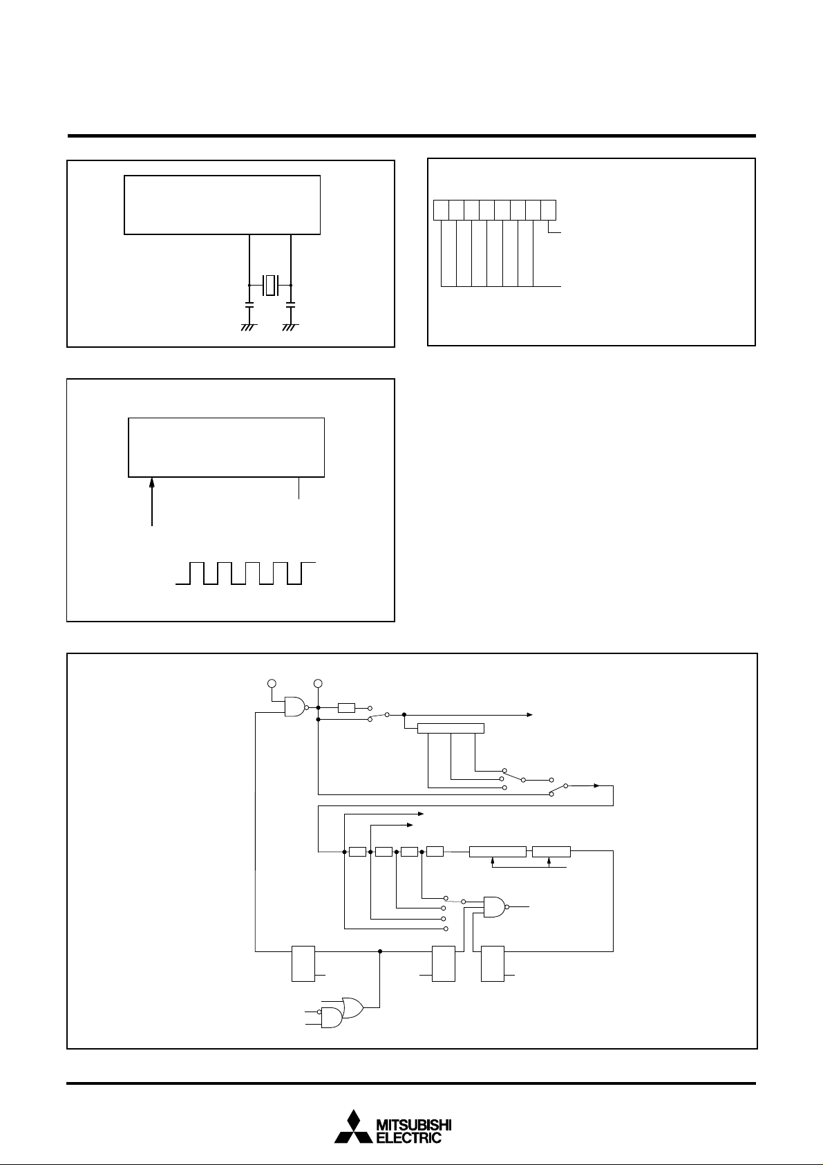
MITSUBISHI MICROCOMPUTERS
38K0 Group
SINGLE-CHIP 8-BIT CMOS MICROCOMPUTER
b 0b 7
M I S R G
X
I N
X
O U T
C
C
I N
O U T
( M I S R G : a d d r e s s 0 F F B
O s c i l l a t i o n s t a b i l i z i n g t i m e s e t a f t e r S T P i n s t r u c t i o n
r e l e a s e d b i t
0 : A u t o m a t i c a l l y s e t “ 0 1
“ F F
1 6
” t o P r e s c a l e r 1 2
1 : A u t o m a t i c a l l y s e t n o t h i n g
N o t u s e d ( i n d e f i n i t e a t r e a d )
1 6
)
1 6
” t o T i m e r 1 ,
Fig. 110 Ceramic resonator or quartz-crystal oscilltor circuit
X
I N
X
O U T
O p e n
E x t e r n a l o s c i l l a t i o n c i r c u i t
CC
V
V
SS
Fig. 111 External clock input circuit
XI
N XO U T
f v c o
U S B c l o c k s e l e c t i o n b i t
P L L
Fig. 112 Structure of MISRG
S
fU
B
1 / 81 / 41 / 6
U S B c l o c k d i v i s i o n
r a t i o n s e l e c t i o n b i t s
f
S Y N
S y s t e m c l o c k s e l e c t i o n b i t
i
fs
o
fA
D
I n t e r r u p t d i s a b l e f l a g l
I n t e r r u p t r e q u e s t
Q
R e s e t
S
R
1 / 2
S T P i n s t r u c t i o n
1 / 2
i n s t r u c t i o n
1 / 2
1 / 2
1 / 81 / 41 / 21 / 1
S y s t e m c l o c k d i v i s i o n
r a t i o n s e l e c t i o n b i t s
S
W I T
R
Q
Fig. 113 System clock generating circuit block diagram (single-chip mode)
P r e s c a l e r 1 2
F F1
6 0
Q
S
R
T i m e r 1
R e s e t o r S T P
i n s t r u c t i o n
11
6
T i m i n g φ ( i n t e r n a l c l o c k )
S T P i n s t r u c t i o n
79
Page 80

R e s e t
MITSUBISHI MICROCOMPUTERS
38K0 Group
SINGLE-CHIP 8-BIT CMOS MICROCOMPUTER
X
I N
8 - d i v i d e m o d e
f (φ) = 0 . 7 5 M H z
C M 7 = 0
C M 6 = 0
C M 5 = 0
P L L C O N [ 4 : 3 ] = 0 0
”
C
M 7“
1 ”← →“ 0
X
I N
2 - d i v i d e m o d e
f (φ) = 3 . 0 M H z
C M 7 = 1
C M 6 = 0
C M 5 = 0
P L L C O N [ 4 : 3 ] = x x
( a r b i t r a r y )
”
N o t e:
S e t P L L C O N [ 4 : 3 ] = 1 0 b e f o r e
s w i t c h i n g t h e s y s t e m c l o c k f r o m X
t o f
C M 7 = 1
C M 6 = 0
C M 5 = 1
S Y N
C
M 5“
1 ”← →“ 0
f (
S Y N
) 2 - d i v i d e m o d e
f (φ) = 6 . 0 M H z
P L L C O N [ 4 : 3 ] = 1 0
CM6
“0”←→“1”
M
0 ”← →“ 1
M
0 ”← →“ 1
C
“
6
C
“
7
”
”
”
6
C
7
“
”
CM6
“0”←→“1”
M
0 ”← →“ 1
M
1 ”← →“ 0
C
“
XIN 4-divide mode
f(φ) = 1.5 MHz
CM7 = 0
CM6 = 0
CM5 = 0
PLLCON [4:3] = xx
(arbitrary)
”
C
M 7“
1 ”← →“ 0
XIN through mode
f(φ) = 1.5 MHz
CM7 = 0
CM6 = 0
CM5 = 0
PLLCON [4:3] = xx
(arbitrary)
”
I N
.
CM6
“0”←→“1”
C
M 5“
1 ”← →“ 0
f(
SYN
) through mode
f(φ) = 12.0 MHz
CM7 = 1
CM6 = 1
CM5 = 1
PLLCON [4:3] = 10
CM5
“0”←→“1”
CM6
“0”←→“1”
Note:
Set PLLCON [4:3] = 00 before switching
the system clock from X
CM5
“0”←→“1”
CM6
“0”←→“1”
Note:
Set PLLCON [4:3] = 01 before switching
the system clock from X
N o t e s
1 : S w i t c h t h e m o d e b y t h e a l l o w s s h o w n b e t w e e n t h e m o d e b l o c k s . ( D o n o t s w i t c h b e t w e e n t h e m o d e s d i r e c t l y
w i t h o u t a n a l l o w . )
2 : S e t t h e U S B c l o c k ( f
3 : D o n o t c h a n g e a d i v i s i o n r a t i o o f U S B c l o c k w h e n u s i n g f
4 : S e e s e c t i o n “ P L L C I R C U I T ” i n d e t a i l s f o r e n a b l i n g / d i s a b l i n g P L L o p e r a t i o n a n d u s a g e n o t e s o f f
5 : S e t t h e s y s t e m c l o c k t o X
6 : I n a l l m o d e s , s w i t c h i n g t o W A I T m o d e i s p o s s i b l e . W h e n i t i s r e l e a s e d , t h e M C U r e t u r n s t o t h e o r i g i n a l m o d e . I n
W A I T m o d e t h e t i m e r s c a n o p e r a t e .
R e m a r k s : T h i s d i a g r a m a s s u m e s t h a t t h e 6 M H z s i g n a l s a r e a p p l i e d t o X
Fig. 114 State transitions of clock
Under planning
f(
SYN
) through mode
f(φ) = 6.0 MHz
CM7 = 1
CM6 = 1
CM5 = 1
IN
to f
SYN
.
IN
to f
SYN
.
U S B
PLLCON [4:3] = 00
f(
SYN
) through mode
f(φ) = 8.0 MHz
CM7 = 1
CM6 = 1
CM5 = 1
PLLCON [4:3] = 01
) t o 4 8 M H z w h e n s w i t c h i n g t h e s y s t e m c l o c k t o f
I N
w h e n e n t e r i n g S T O P m o d e .
Note:
Set PLLCON [4:3] = 00 before switching
the system clock from X
Note:
Set PLLCON [4:3] = 01 before switching
the system clock from X
S Y N
a s t h e s y s t e m c l o c k .
I N
p i n .
C M 5
“ 0 ”← →“ 1 ”
IN
CM5
“0”←→“1”
IN
S Y N
.
to f
to f
SYN
SYN
.
.
S Y N
.
80
Page 81

MITSUBISHI MICROCOMPUTERS
38K0 Group
SINGLE-CHIP 8-BIT CMOS MICROCOMPUTER
FLASH MEMORY MODE
The 38K0 group’s flash memory version has an internal new
DINOR (DIvided bit line NOR) flash memory that can be rewritten
with a single power source when VCC is 4.5 to 5.25 V , and 2 power
sources when VCC is 3.0 to 4.5 V.
For this flash memory, three flash memory modes are available in
which to read, program, and erase: the parallel I/O and standard
serial I/O modes in which the flash memory can be manipulated
using a programmer and the CPU rewrite mode in which the flash
memory can be manipulated by the Central Processing Unit
(CPU).
Table 8 Summary of 38K0 group’s flash memory version
Item
Power source voltage (Vcc)
Program/Erase VPP voltage (VPP)
Flash memory mode
Erase block division User ROM area
Boot ROM area
Program method
Erase method
Program/Erase control method
Number of commands
Number of program/Erase times
Data retention period
ROM code protection
Notes 1: In the parallel I/O mode or the standard serial I/O mode, use the exclusive external equipment flash programmer which supports the 38K2 Group
(flash memory version).
2: The Boot ROM area has had a standard serial I/O mode control program stored in it when shipped from the factory. This Boot ROM area can be re-
written in only parallel I/O mode.
3.00 – 5.25 V (Program and erase in 4.00 to 5.25 V of Vcc.)
3.00 – 4.00 V (Program and erase in 3.00 to 5.25 V of Vcc.)
4.50 – 5.25 V
3 modes; Flash memory can be manipulated as follows:
•CPU rewrite mode: Manipulated by the Central Processing Unit (CPU).
•Parallel I/O mode: Manipulated using an external programmer (Note 1)
•Standard serial I/O mode: Manipulated using an external programmer (Note 1)
1 block (32 Kbytes)
1 block (4 Kbytes) (Note 2)
Byte program
Batch erasing
Program/Erase control by software command
6 commands
100 times
10 years
Available in parallel I/O mode and standard serial I/O mode
Summary
Table 8 lists the summary of the 38K0 group’s flash memory version.
This flash memory version has some blocks on the flash memory
as shown in Figure 115 and each block can be erased. The flash
memory is divided into User ROM area and Boot ROM area.
In addition to the ordinary User ROM area to store the MCU operation control program, the flash memory has a Boot ROM area
that is used to store a program to control rewriting in CPU rewrite
and standard serial I/O modes. This Boot ROM area has had a
standard serial I/O mode control program stored in it when
shipped from the factory. However, the user can write a rewrite
control program in this area that suits the user’s application system. This Boot ROM area can be rewritten in only parallel I/O
mode.
Specifications
81
Page 82

MITSUBISHI MICROCOMPUTERS
38K0 Group
SINGLE-CHIP 8-BIT CMOS MICROCOMPUTER
(1) CPU Rewrite Mode
In CPU rewrite mode, the internal flash memory can be operated
on (read, program, or erase) under control of the Central Processing Unit (CPU).
In CPU rewrite mode, only the User ROM area shown in Figure
115 can be rewritten; the Boot ROM area cannot be rewritten.
Make sure the program and block erase commands are issued for
only the User ROM area and each block area.
The control program for CPU rewrite mode can be stored in either
User ROM or Boot ROM area. In the CPU rewrite mode, because
the flash memory cannot be read from the CPU, the rewrite control program must be transferred to internal RAM area to be
executed before it can be executed.
U s e r R O M a r e a
16
8000
F F F F
1 6
B l o c k 1 : 3 2 K b y t e s
Microcomputer Mode and Boot Mode
The control program for CPU rewrite mode must be written into
the User ROM or Boot ROM area in parallel I/O mode beforehand.
(If the control program is written into the Boot ROM area, the standard serial I/O mode becomes unusable.)
See Figure 115 for details about the Boot ROM area.
Normal microcomputer mode is entered when the microcomputer
is reset with pulling CNVSS pin low. In this case, the CPU starts
operating using the control program in the User ROM area.
When the microcomputer is reset by pulling the P16 (CE) pin high,
the CNVSS pin high, the CPU starts operating using the control
program in the Boot ROM area. This mode is called the “Boot”
mode.
Block Address
Block addresses refer to the maximum address of each block.
These addresses are used in the block erase command.
B o o t R O M a r e a
F0 0 0
F F F F
1 6
1 6
4 Kb y t e s
Notes 1: T he B oot ROM area can be rewritten in only par allel I/O mode. (Access to any oth er
areas is inhibited.)
2: To specify a block, use the maxim um address in the bloc k .
Fig. 115 Block diagram of built-in flash memory
82
Page 83

MITSUBISHI MICROCOMPUTERS
38K0 Group
SINGLE-CHIP 8-BIT CMOS MICROCOMPUTER
Outline Performance (CPU Rewrite Mode)
CPU rewrite mode is usable in the single-chip or Boot mode. The
only User ROM area can be rewritten in CPU rewrite mode.
In CPU rewrite mode, the CPU erases, programs and reads the internal flash memory as instructed by software commands. This
rewrite control program must be transferred to a memory such as
the internal RAM before it can be executed.
The MCU enters CPU rewrite mode by applying 4.50 V to 5.25 V
to the CNVSS pin and setting “1” to the CPU Rewrite Mode Select
Bit (bit 1 of address 0FFE16). Software commands are accepted
once the mode is entered.
Use software commands to control program and erase operations.
Whether a program or erase operation has terminated normally or
in error can be verified by reading the status register.
Figure 116 shows the flash memory control register.
Bit 0 is the RY/BY status flag used exclusively to read the operating status of the flash memory. During programming and erase
operations, it is “0” (busy). Otherwise, it is “1” (ready). This is
equivalent to the RY/BY pin function in parallel I/O mode.
Bit 1 is the CPU Rewrite Mode Select Bit. When this bit is set to
“1”, the MCU enters CPU rewrite mode. Software commands are
accepted once the mode is entered. In CPU rewrite mode, the
CPU becomes unable to access the internal flash memory directly.
Therefore, use the control program in a memory other than internal flash memory for write to bit 1. To set this bit to “1”, it is
necessary to write “0” and then write “1” in succession. The bit can
be set to “0” by only writing “0”.
Bit 2 is the CPU Rewrite Mode Entry Flag. This flag indicates “1” in
CPU rewrite mode, so that reading this flag can check whether
CPU rewrite mode has been entered or not.
Bit 3 is the flash memory reset bit used to reset the control circuit
of internal flash memory. This bit is used when exiting CPU rewrite
mode and when flash memory access has failed. When the CPU
Rewrite Mode Select Bit is “1”, setting “1” for this bit resets the
control circuit. To set this bit to “1”, it is necessary to write “0” and
then write “1” in succession. To release the reset, it is necessary
to set this bit to “0”.
Bit 4 is the User Area/Boot Area Select Bit. When this bit is set to
“1”, Boot ROM area is accessed, and CPU rewrite mode in Boot
ROM area is available. In Boot mode, this bit is set to “1” automatically. Reprogramming of this bit must be in a memory other
than internal flash memory.
Figure 117 shows a flowchart for setting/releasing CPU rewrite
mode.
b0b 7
Flash memory control register (address 0FFE16)
FMCR
(Note 1)
RY/BY status flag
0: Busy (being written or erased)
1: Ready
CPU rewrite mode select bit (Note 2)
0: Normal mode (Software commands invalid)
1: CPU rewrite mode (Software commands acceptable)
CPU rewrite mode entry flag
0: Normal mode (Software commands invalid)
1: CPU rewrite mode
Flash memory reset bit (Note 3)
0: Normal operation
1: Reset
User area / Boot area select bit (Note 4)
0: User ROM area accessed
1: Boot ROM area accessed
Reserved bits (indefinite at read/ “0” at write)
N o t e s1: T h e c o n t e n t s o f f l a s h m e m o r y c o n t r o l r e g i s t e r a r e “ X X X 0 0 0 0 1 ” j u s t a f t e r r e s e t r e l e a s e .
2: F o r t h i s b i t t o b e s e t t o “ 1 ” , t h e u s e r n e e d s t o w r i t e “ 0 ” a n d t h e n “ 1 ” t o i t i n s u c c e s s i o n . I f i t i s n o t
t h i s p r o c e d u r e , t h i s b i t w i l l n o t b e s e t t o ” 1 ” . A d d i t i o n a l l y , i t i s r e q u i r e d t o e n s u r e t h a t n o i n t e r r u p t
w i l l b e g e n e r a t e d d u r i n g t h a t i n t e r v a l .
U s e t h e c o n t r o l p r o g r a m i n t h e a r e a e x c e p t t h e b u i l t - i n f l a s h m e m o r y f o r w r i t e t o t h i s b i t .
3: T h i s b i t i s v a l i d w h e n t h e C P U r e w r i t e m o d e s e l e c t b i t i s “ 1 ” . S e t t h i s b i t 3 t o “ 0 ” s u b s e q u e n t l y a f t e r
s e t t i n g b i t 3 t o “ 1 ” .
4: U s e t h e c o n t r o l p r o g r a m i n t h e a r e a e x c e p t t h e b u i l t - i n f l a s h m e m o r y f o r w r i t e t o t h i s b i t .
Fig. 116 Structure of flash memory control register
83
Page 84

MITSUBISHI MICROCOMPUTERS
SINGLE-CHIP 8-BIT CMOS MICROCOMPUTER
S t a r t
S i n g l e - c h i p m o d e o r B o o t m o d e ( N o t e 1 )
S e t C P U m o d e r e g i s t e r ( N o t e 2 )
T r a n s f e r C P U r e w r i t e m o d e c o n t r o l p r o g r a m t o
m e m o r y o t h e r t h a n i n t e r n a l f l a s h m e m o r y
J u m p t o c o n t r o l p r o g r a m t r a n s f e r r e d i n m e m o r y
o t h e r t h a n i n t e r n a l f l a s h m e m o r y
( S u b s e q u e n t o p e r a t i o n s a r e e x e c u t e d b y c o n t r o l
p r o g r a m i n t h i s m e m o r y )
38K0 Group
Set CPU rewrite mode select bit to “1” (by
writing “0” and then “1” in succession)
C h e c k C P U r e w r i t e m o d e e n t r y f l a g
U s i n g s o f t w a r e c o m m a n d e x e c u t e e r a s e ,
p r o g r a m , o r o t h e r o p e r a t i o n
Execute read array command or reset flash
memory by setting flash memory reset bit (by
writing “1” and then “0” in succession) (Note 3)
Write “0” to CPU rewrite mode select bit
E n d
N o t e s1: W h e n s t a r t i n g t h e M C U i n t h e s i n g l e - c h i p m o d e o r m e m o r y e x p a n s i o n m o d e , s u p p l y
4 . 5 V t o 5 . 2 5 V t o t h e C N V s s p i n u n t i l c h e c k i n g t h e C P U r e w r i t e m o d e e n t r y f l a g .
2: S e t t h e s y s t e m c l o c k d i v i s i o n r a t i o n s e l e c t i o n b i t s o f C P U m o d e r e g i s t e r ( b i t s 6 a n d
7 a t a d d r e s s 0 0 3 B
3: B e f o r e e x i t i n g t h e C P U r e w r i t e m o d e a f t e r c o m p l e t i n g e r a s e o r p r o g r a m o p e r a t i o n ,
a l w a y s b e s u r e t o e x e c u t e t h e r e a d a r r a y c o m m a n d o r r e s e t t h e f l a s h m e m o r y .
1 6
) .
Fig. 117 CPU rewrite mode set/release flowchart
84
Page 85

Notes on CPU Rewrite Mode
Take the notes described below when rewriting the flash memory
in CPU rewrite mode.
●Operation speed
During CPU rewrite mode, set the internal clock φ to 1.5 MHz or
less using the system clock division ratio selection bits (bits 6 and
7 of address 003B16).
●Instructions inhibited against use
The instructions which refer to the internal data of the flash
memory cannot be used during CPU rewrite mode .
●Interrupts inhibited against use
The interrupts cannot be used during CPU rewrite mode because
they refer to the internal data of the flash memory.
●Watchdog timer
If the watchdog timer has been already activated, internal reset
due to an underflow will not occur because the watchdog timer is
surely cleared during program or erase.
MITSUBISHI MICROCOMPUTERS
38K0 Group
SINGLE-CHIP 8-BIT CMOS MICROCOMPUTER
●Reset
Reset is always valid. The MCU is activated using the boot mode
at release of reset in the condition of CNVss = “H”, so that the program will begin at the address which is stored in addresses
FFFC16 and FFFD16 of the boot ROM area.
85
Page 86

MITSUBISHI MICROCOMPUTERS
?
38K0 Group
SINGLE-CHIP 8-BIT CMOS MICROCOMPUTER
Software Commands
Table 9 lists the software commands.
After setting the CPU Rewrite Mode Select Bit to “1”, write a software command to specify an erase or program operation.
Each software command is explained below.
●Read Array Command (FF16)
The read array mode is entered by writing the command code
“FF16” in the first bus cycle. When an address to be read is input in
one of the bus cycles that follow, the contents of the specified address are read out at the data bus (D0 to D7).
The read array mode is retained intact until another command is
written.
●Read Status Register Command (7016)
When the command code “7016” is written in the first bus cycle,
the contents of the status register are read out at the data bus (D0
to D7) by a read in the second bus cycle.
The status register is explained in the next section.
●Clear Status Register Command (5016)
This command is used to clear the bits SR4 and SR5 of the status
register after they have been set. These bits indicate that operation has ended in an error. To use this command, write the
command code “5016” in the first bus cycle.
●Program Command (4016)
Program operation starts when the command code “4016” is written in the first bus cycle. Then, if the address and data to program
are written in the 2nd bus cycle, the control circuit of flash memory
(data programming and verification) will start a program.
Whether the write operation is completed can be confirmed by
reading the status register or the RY/BY Status Flag. When the
program starts, the read status register mode is entered automatically and the contents of the status register is read at the data bus
(DB0 to DB7). The status register bit 7 (SR7) is set to “0” at the
same time the write operation starts and is returned to “1” upon
completion of the write operation. In this case, the read status register mode remains active until the read array command (FF16) is
written.
Table 9 List of software commands (CPU rewrite mode)
Command
R e a d a r r a y
R e a d s t a t u s r e g i s t e r
C l e a r s t a t u s r e g i s t e r
P r o g r a m
_____
C y c l e n u m b e r
1
2
1
2
M o d eA d d r e s s
Write
Write
Write
Write
During the program movement, The RY/BY Status Flag of flash
memory control register is set to “0”. When the program completes, it becomes “1”.
At program end, program results can be checked by reading the
status register.
____
S t a r t
W r i t e
W r i t e 4 0
W r i t e a d d r e s s
W r i t e d a t a
1 6
S t a t u s r e g i s t e r
r e a d
S R 7 = 1
o r
R Y / B Y = 1 ?
Y E S
SR4 = 0 ?
N O
NO
Program
error
Y E S
Program
completed
Fig. 118 Program flowchart
First bus cycle Second bus cycle
X
(Not e 4)
X
X
X
(D
D a t a
0
to D7)
FF
70
50
4 0
M o d eA d d r e s s
16
16
16
W r i t e
1 6
W A
XSRDR e a d
( N o t e 2 )
(D
W D
Data
0
to D7)
(Not e 1)
(Not e 2)
E r a s e a l l b l o c k s20
Block erase 2 0
2
2
Write X 20
Write D0
X
X
16
1 6
W r i t e
W r i t eBA
(Not e 3)
16
16
N o t e s 1 : SRD = Status Register Data
2: WA = Write Address, WD = Write Data
3: BA = Block Address to be erased (Input the maximum address of each block.)
4: X denotes a given address in the User ROM area .
86
Page 87

●Erase All Blocks Command (2016/2016)
?
SR
?
By writing the command code “2016” in the first bus cycle and the
confirmation command code “2016” in the second bus cycle that
follows, the operation of erase all blocks (erase and erase verify)
starts.
Whether the erase all blocks command is terminated can be confirmed by reading the status register or the RY/BY Status Flag of
____
flash memory control register. When the erase all blocks operation
starts, the read status register mode is entered automatically and
the contents of the status register can be read out at the data bus
(D0 to D7). The status register bit 7 (SR7) is set to “0” at the same
time the erase operation starts and is returned to “1” upon completion of the erase operation. In this case, the read status register
mode remains active until the read array command (FF16) is written.
The RY/BY Status Flag is “0” during erase operation and “1” when
____
the erase operation is completed as is the status register bit 7.
After the erase all blocks end, erase results can be checked by
reading the status register. For details, refer to the section where
the status register is detailed.
●Block Erase Command (2016/D016)
By writing the command code “2016” in the first bus cycle and the
confirmation command code “D016” and the block address in the
second bus cycle that follows, the block erase (erase and erase
verify) operation starts for the block address of the flash memory
to be specified.
Whether the block erase operation is completed can be confirmed
by reading the status register or the RY/BY Status Flag of flash
____
memory control register. At the same time the block erase operation starts, the read status register mode is automatically entered,
so that the contents of the status register can be read out. The
status register bit 7 (SR7) is set to “0” at the same time the block
erase operation starts and is returned to “1” upon completion of
the block erase operation. In this case, the read status register
mode remains active until the read array command (FF16) is written.
The RY/BY Status Flag is “0” during block erase operation and “1”
____
when the block erase operation is completed as is the status register bit 7.
After the block erase ends, erase results can be checked by reading the status register. For details, refer to the section where the
status register is detailed.
MITSUBISHI MICROCOMPUTERS
SINGLE-CHIP 8-BIT CMOS MICROCOMPUTER
S t a r t
W r i t e 2 0
Write
S t a t u s r e g i s t e r
RY/BY = 1 ?
SR5 = 0
Erase completed
Fig. 119 Erase flowchart
1 6
2 0
1 6
/ D 0
1 6
B l o c k a d d r e s s
r e a d
7 = 1
or
Y E S
YES
2 0
D 0
N O
N O
38K0 Group
1 6
: E r a s e a l l b l o c k s
1 6
: B l o c k e r a s e
E r a s e e r r o r
87
Page 88

MITSUBISHI MICROCOMPUTERS
38K0 Group
SINGLE-CHIP 8-BIT CMOS MICROCOMPUTER
Status Register (SRD)
The status register shows the operating status of the flash
memory and whether erase operations and programs ended successfully or in error. It can be read in the following ways:
(1) By reading an arbitrary address from the User ROM area after
writing the read status register command (7016)
(2) By reading an arbitrary address from the User ROM area in the
period from when the program starts or erase operation starts
to when the read array command (FF16) is input.
Also, the status register can be cleared by writing the clear status
register command (5016).
After reset, the status register is set to “8016”.
Table 10 shows the status register. Each bit in this register is explained below.
•Sequencer status (SR7)
The sequencer status indicates the operating status of the flash
memory. This bit is set to “0” (busy) during write or erase operation
and is set to “1” when these operations ends.
After power-on, the sequencer status is set to “1” (ready).
Table 10 Definition of each bit in status register
Each bit of
SRD0 bits
SR7 (bit7)
SR6 (bit6)
SR5 (bit5)
SR4 (bit4)
SR3 (bit3)
SR2 (bit2)
SR1 (bit1)
SR0 (bit0)
Status name
Sequencer status
Reserved
Erase status
Program status
Reserved
Reserved
Reserved
Reserved
•Erase status (SR5)
The erase status indicates the operating status of erase operation.
If an erase error occurs, it is set to “1”. When the erase status is
cleared, it is set to “0”.
•Program status (SR4)
The program status indicates the operating status of write operation. When a write error occurs, it is set to “1”.
The program status is set to “0” when it is cleared.
If “1” is written for any of the SR5 and SR4 bits, the program,
erase all blocks, and block erase commands are not accepted.
Before executing these commands, execute the clear status register command (5016) and clear the status register.
Definition
“1” “0”
Ready
Terminated in error
Terminated in error
-
-
-
-
Terminated normally
Terminated normally
Busy
-
-
-
-
-
88
Page 89

Full Status Check
By performing full status check, it is possible to know the execution results of erase and program operations. Figure 120 shows a
full status check flowchart and the action to be taken when each
error occurs.
Read status register
MITSUBISHI MICROCOMPUTERS
38K0 Group
SINGLE-CHIP 8-BIT CMOS MICROCOMPUTER
S R 4 = 1 a n d
S R5 = 1 ?
N O
S R 5 = 0 ?
Y E S
S R 4 = 0 ?
YES
E n d ( b l o c k e r a s e , p r o g r a m )
Y E S
N O
N O
C o m m a n d
s e q u e n c e e r r o r
Erase error
P r o g r a m e r r o r
Execute the clear status register command (50
to clear the status register. Try performing the
operation one more time after confirming that the
command is entered correctly.
Should an erase error occur, the block in error
cannot be used.
Should a program error occur, the block in error
cannot be used.
Note: When one of SR5 and SR4 is set to “1”, none of the program, erase all blocks,
and block erase commands is accepted. Execute the clear status register
16
command (50
Fig. 120 Full status check flowchart and remedial procedure for errors
) before executing these commands.
16
)
89
Page 90
MITSUBISHI MICROCOMPUTERS
38K0 Group
SINGLE-CHIP 8-BIT CMOS MICROCOMPUTER
Functions To Inhibit Rewriting Flash Memory
Version
To prevent the contents of internal flash memory from being read
out or rewritten easily, this MCU incorporates a ROM code protect
function for use in parallel I/O mode and an ID code check function for use in standard serial I/O mode.
●ROM Code Protect Function
The ROM code protect function is the function to inhibit reading
out or modifying the contents of internal flash memory by using
the ROM code protect control register (address FFDB16) in parallel I/O mode. Figure 121 shows the ROM code protect control
register (address FFDB16). (This address exists in the User ROM
area.)
b 0b 7
R O M c o d e p r o t e c t c o n t r o l r e g i s t e r ( a d d r e s s F F D B
R O M C P
Reserved bits (“1” at read/write)
ROM code protect level 2 set bits (ROMCP2) (Notes 1, 2)
b3b2
0 0: Protect enabled
0 1: Protect enabled
1 0: Protect enabled
1 1: Protect disabled
ROM code protect reset bits
b5b4
0 0: Protect removed
0 1: Protect set bits effective
1 0: Protect set bits effective
1 1: Protect set bits effective
ROM code protect level 1 set bits (ROMCP1) (Note 1)
b7b6
0 0: Protect enabled
0 1: Protect enabled
1 0: Protect enabled
1 1: Protect disabled
Notes 1: When ROM code protect is turned on, the internal flash memory is protected
against readout or modification in parallel I/O mode.
2: When ROM code protect level 2 is turned on, ROM code readout by a shipment
inspection LSI tester, etc. also is inhibited.
3: The ROM code protect reset bits can be used to turn off ROM code protect level 1
and ROM code protect level 2. However, since these bits cannot be modified in
parallel I/O mode, they need to be rewritten in serial I/O mode or CPU rewrite
mode.
If one or both of the pair of ROM Code Protect Bits is set to “0”,
the ROM code protect is turned on, so that the contents of internal
flash memory are protected against readout and modification. The
ROM code protect is implemented in two levels. If level 2 is selected, the flash memory is protected even against readout by a
shipment inspection LSI tester, etc. When an attempt is made to
select both level 1 and level 2, level 2 is selected by default.
If both of the two ROM Code Protect Reset Bits are set to “00”, the
ROM code protect is turned off, so that the contents of internal
flash memory can be read out or modified. Once the ROM code
protect is turned on, the contents of the ROM Code Protect Reset
Bits cannot be modified in parallel I/O mode. Use the serial I/O or
CPU rewrite mode to rewrite the contents of the ROM Code Protect Reset Bits.
1 6
)
(Note 3)
Fig. 121 Structure of ROM code protect control register
90
Page 91
ID Code Check Function
Use this function in standard serial I/O mode. When the contents
of the flash memory are not blank, the ID code sent from the programmer is compared with the ID code written in the flash memory
to see if they match. If the ID codes do not match, the commands
sent from the programmer are not accepted. The ID code consists
of 8-bit data, and its areas are FFD416 to FFDA16. Write a program which has had the ID code preset at these addresses to the
flash memory.
Address
FFD4
16
ID1
MITSUBISHI MICROCOMPUTERS
38K0 Group
SINGLE-CHIP 8-BIT CMOS MICROCOMPUTER
FFD5
16
FFD6
16
FFD7
16
FFD8
16
FFD9
16
FFDA
16
FFDB
16
ROM cord protect control
Interrupt vector area
Fig. 122 ID code store addresses
ID2
ID3
ID4
ID5
ID6
ID7
91
Page 92

(2) Parallel I/O Mode
Parallel I/O mode is the mode which parallel output and input software command, address, and data required for the operations
(read, program, erase, etc.) to a built-in flash memory. Use the exclusive external equipment flash programmer which supports the
38K0 Group (flash memory version). Refer to each programmer
maker’s handling manual for the details of the usage.
User ROM and Boot ROM Areas
In parallel I/O mode, the user ROM and boot ROM areas shown in Figure 115 can be rewritten. Both areas of flash memory can be operated
on in the same way.
The boot ROM area is 4 Kbytes in size. It is located at addresses
F00016 through FFFF16. Make sure program and block erase operations are always performed within this address range. (Access to any
location outside this address range is prohibited.)
In the Boot ROM area, an erase block operation is applied to only
one 4 Kbyte block.
The boot ROM area has had a standard serial I/O mode control program stored in it when shipped from the Mitsubishi factory. Therefore, using the device in standard serial I/O mode, you must perform
program and block erase in the user ROM area.
MITSUBISHI MICROCOMPUTERS
38K0 Group
SINGLE-CHIP 8-BIT CMOS MICROCOMPUTER
92
Page 93

MITSUBISHI MICROCOMPUTERS
38K0 Group
SINGLE-CHIP 8-BIT CMOS MICROCOMPUTER
(3) Standard Serial I/O Mode
The standard serial I/O mode inputs and outputs the software
commands, addresses and data needed to operate (read, program, erase, etc.) the internal flash memory. This I/O is clock
synchronized serial. This mode requires a purpose-specific peripheral unit.The standard serial I/O mode is different from the
parallel I/O mode in that the CPU controls flash memory rewrite
(uses the CPU rewrite mode), rewrite data input and so forth. The
standard serial I/O mode is started by connecting “H” to the P16
(CE) pin and “H” to the P42 (SCLK) pin and “H” to the CNVSS (VPP)
pin (apply 4.5 V to 5.25 V to Vpp from an external source), and releasing the reset operation. (In the ordinary microcomputer mode,
set CNVss pin to “L” level.)
This control program is written in the Boot ROM area when the
product is shipped from Mitsubishi. Accordingly, make note of the
fact that the standard serial I/O mode cannot be used if the Boot
ROM area is rewritten in parallel I/O mode. Figure 123 shows the
pin connections for the standard serial I/O mode.
In standard serial I/O mode, serial data I/O uses the four serial I/O
pins SCLK, RxD, TxD and SRDY (BUSY). The SCLK pin is the transfer clock input pin through which an external transfer clock is
input. The TxD pin is for CMOS output. The SRDY (BUSY) pin outputs “L” level when ready for reception and “H” level when
reception starts.
Serial data I/O is transferred serially in 8-bit units.
In standard serial I/O mode, only the User ROM area shown in
Figure 115 can be rewritten. The Boot ROM area cannot.
In standard serial I/O mode, a 7-byte ID code is used. When there
is data in the flash memory, commands sent from the peripheral
unit (programmer) are not accepted unless the ID code matches.
Outline Performance (Standard Serial I/O
Mode)
In standard serial I/O mode, software commands, addresses and
data are input and output between the MCU and peripheral units
(serial programer, etc.) using 4-wire clock-synchronized serial I/O.
In reception, software commands, addresses and program data
are synchronized with the rise of the transfer clock that is input to
the SCLK pin, and are then input to the MCU via the RxD pin. In
transmission, the read data and status are synchronized with the
fall of the transfer clock, and output from the TxD pin.
The TxD pin is for CMOS output. Transfer is in 8-bit units with LSB
first.
When busy, such as during transmission, reception, erasing or
program execution, the SRDY (BUSY) pin is “H” level. Accordingly,
always start the next transfer after the SRDY (BUSY) pin is “L”
level.
Also, data and status registers in a memory can be read after inputting software commands. Status, such as the operating state of
the flash memory or whether a program or erase operation ended
successfully or not, can be checked by reading the status register.
Here following explains software commands, status registers, etc.
93
Page 94
Table 11 Description of pin function (Standard Serial I/O Mode)
Pin name Signal name I/O
VCC,VSS Power supply
VCCE Power supply
CNVSS VPP I
CNVSS2 CNVSS2I
VREF Analog reference voltage I
DVCC, PVCC Analog power supply
PVSS Analog power supply
RESET Reset input I
XIN Clock input I
XOUT Clock output O
USBVREF USB reference voltage input I
TrON USB reference voltage output
D0+,D0- USB upstream input I/O
P00 to P07 Input port P0 I
P10 to P15 Input port P1 I
P16 Input port P1 I
P17 Input port P1 I
P20 to P27 Input port P2 I
P30 to P37 Input port P3 I
P40 RxD input I
P41 TxD output O
P42 SCLK input I
P43 BUSY output O
P50 to P57 Input port P5 I
P60 to P63 Input port P6 I
Function
Apply 3.00 to 5.25 V to the Vcc pin and 0 V to the Vss pin.
Connect this pin to Vcc.
Connect this pin to VPP (VPP = 4.50 to 5.25 V).
Connect this pin to Vss.
Connect this pin to Vcc when not using.
Connect this pin to Vcc.
Connect this pin to Vss.
To reset, input “L” level for 20 cycles or longer clocks of φ.
Connect a ceramic or crystal resonator between the XIN and XOUT pins. When
entering an externally drived clock, enter it from XIN and leave XOUT open.
Connect this pin to Vcc when not using.
Leave this pin open when not using.
Input “L” level when not using.
Input “L” or “H” level, or keep open.
Input “L” or “H” level, or keep open.
Input “L” or “H” level, or keep open. Input “H” level only at release of reset.
Input “L” or “H” level, or keep open.
Input “L” or “H” level, or keep open.
Input “L” or “H” level, or keep open.
This is a serial data input pin.
This is a serial data output pin.
This is a serial clock input pin.Input “H” level only at release of reset.
This is a BUSY output pin.
Input “L” or “H” level, or keep open.
Input “L” or “H” level, or keep open.
MITSUBISHI MICROCOMPUTERS
38K0 Group
SINGLE-CHIP 8-BIT CMOS MICROCOMPUTER
94
Page 95
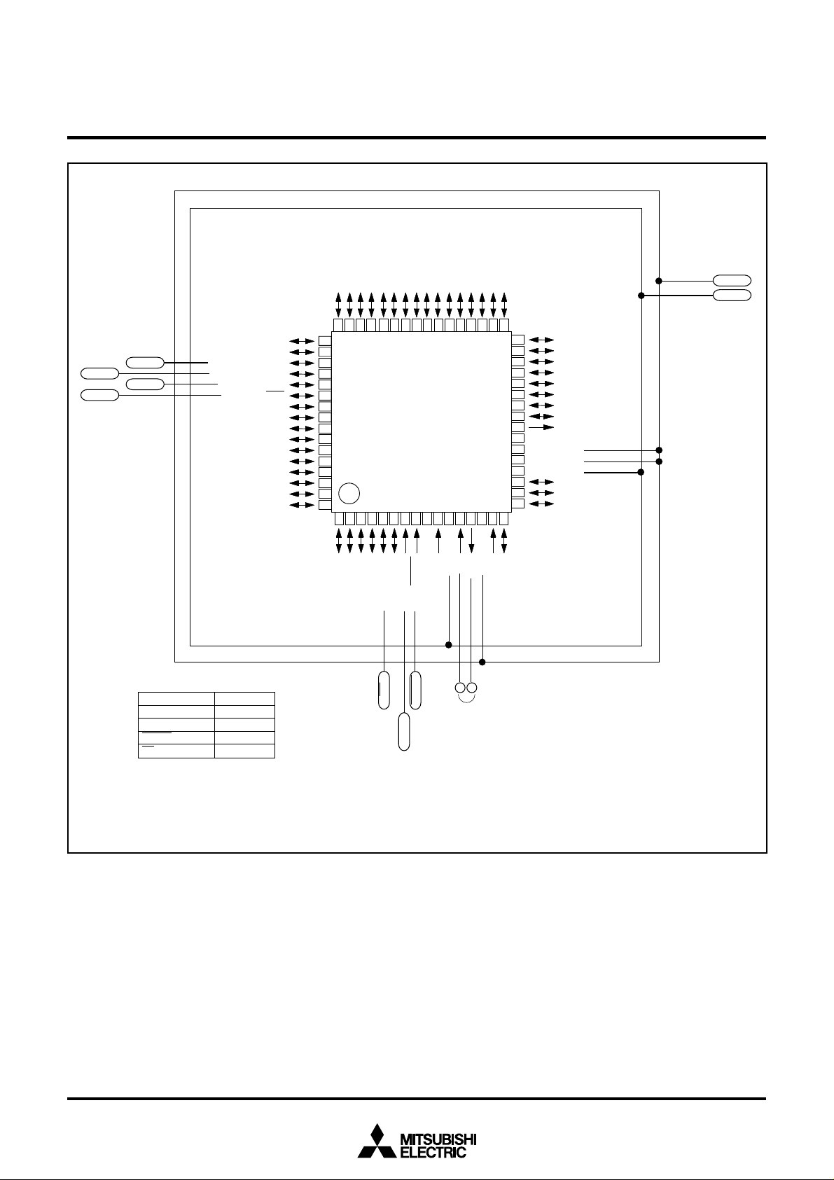
MITSUBISHI MICROCOMPUTERS
38K0 Group
SINGLE-CHIP 8-BIT CMOS MICROCOMPUTER
R0
T0
T1
02
05
01P
P
03P
04P
55
P
56P
57P
00P
54P
50/
52/
51/
P
26P
27P
I N
P
P
53P
I N
P
C N T
V c c
V s s
TXD
B U S Y
6
8
4
74
4 9
5 0
5 1
5 2
K
5 3
5 4
Y
5 5
5 6
M38K09F8FP/HP
5 7
5 8
5 9
60
6 1
62
6 3
6 4
123
N3
N2
N4
Q2/
Q3/
Q4/
13/
14/
12/
P
P
P
D
D
D
A
A
A
RXD
SCLK
P 40/ EXD R E Q / RXD
1/
EXD A C K / TXD
P 4
L
P 4
2/
EXT C / SC
D
P 43/ EXA1/ SR
P 33/ EXI N T
4/
P 3
5/EXWR
P3
6/
P 3
7/EXA0
P3
D
P 1
0/
Q0/ A N0
P 11/ D Q1/ A N1
P06
P07
P 30
P 31
P32
EXC S
EXR D
Mode setup method
Signal Value
c c
. 5 t o 5 . 2 5
C N V s s4
C L K V
S
RESET Vss → Vcc
V
(Note 2)
(Note 1)
CE Vcc (Note 2)
Notes 1: Connect to Vcc in the case of Vcc = 4.5 V to 5.25 V.
Connect to V
2: Supply Vcc at releasimg Reset.
PP (= 4.5 V to 5.25 V) in the case of Vcc = 4.0 V to 4. 5 V .
Package outline: 64P6U-A, 64P6Q-A
4
4
54
4
N5
Q5/
15/
P
D
A
1
4
24
34
5
N6
Q6/
16/
P
A
D
D
A
E
C
94
04
789
6
01
S
T
CE
N7
VS
VC
C
R
Q7/
N
17/
P
E
E S E
T
R
E S E
Connect to oscillator circuit.
P
VP
83
1
1
F
S
R
VS
V
4
3
3
3
3
53
63
73
2
1
31
N
XI
U
3 2
3 1
3 0
2 9
2 8
2 7
2 6
2 5
24
2 3
2 2
2 1
2 0
19
1 8
1 7
5
4
6
1
1
1
T
C
S2
D0)
VC
XO
VS
0(
C
6
P
L E
N
P 25
P 24
P 23
P 22
P21
P 2
0
D 0 D 0 +
T r O N
E
U S B VR
D VC
C
P VC
C
S S
P V
P63(LED3)
L E
2(
D2)
P 6
P 61( L E D1)
F
Fig. 123 Pin connection diagram in standard serial I/O mode (1)
95
Page 96

MITSUBISHI MICROCOMPUTERS
38K0 Group
SINGLE-CHIP 8-BIT CMOS MICROCOMPUTER
Software Commands
Table 12 lists software commands. In standard serial I/O mode,
erase, program and read are controlled by transferring software
commands via the RxD pin. Software commands are explained
Table 12 Software commands (Standard serial I/O mode)
Control command
1 Page read
2 Page program 4116 Address
3 Erase all blocks A716 D016
4 Read status register 7016
5 Clear status register 5016
6 ID check function F516 Acceptable
7 Download function FA16 Size
8 Version data output function FB16
9 Boot ROM area output
function
Notes1: Shading indicates transfer from the internal flash memory microcomputer to a programmer. All other data is transferred from a programmer to the in-
ternal flash memory microcomputer.
2: SRD refers to status register data. SRD1 refers to status register 1 data.
3: All commands can be accepted when the flash memory is totally blank.
4: Address low is A
0 to A7; Address middle is A8 to A15; Address high is A16 to A23. Address-high A16 to A23 are always “0016”.
1st byte
transfer
FF16
FC16
2nd byte
Address
(middle)
(middle)
SRD
output
Address
(low)
(low)
Version
data
output
Address
(middle)
3rd byte
Address
(high)
Address
(high)
SRD1
output
Address
(middle)
(high)
Version
output
Address
Size
data
(high)
here below. Basically, the software commands of the standard serial I/O mode are the same as that of the parallel I/O mode, but the
block erase function is excluded, and 4 commands are added: ID
check, download, version data output and Boot ROM area output
functions.
4th byte
Data
output
Data
input
Address
(high)
Check-
sum
Version
data
output
Data
output
5th byte
Data
output
Data
input
ID size ID1 To ID7
Data
inputTorequired
Version
data
output
Data
output
6th byte
Data
output
Data
input
number
of times
Version
data
output
Data
output
.....
Data
output to
259th byte
Data input
to 259th
byte
Version
data output
to 9th byte
Data
output to
259th byte
When ID is
not verified
Not
acceptable
Not
acceptable
Not
acceptable
Acceptable
Not
acceptable
Not
acceptable
Acceptable
Not
acceptable
96
Page 97

MITSUBISHI MICROCOMPUTERS
38K0 Group
SINGLE-CHIP 8-BIT CMOS MICROCOMPUTER
The contents of software commands are explained as follows.
●Page Read Command
This command reads the specified page (256 bytes) in the flash
memory sequentially one byte at a time. Execute the page read
command as explained here following.
S
C L K
A
8
R x D
F F
1 6
t o
A
1 5
T x D
S
R D Y
( B U S Y )
(1) Transfer the “FF16” command code with the 1st byte.
(2) Transfer addresses A8 to A15 and A16 to A23 with the 2nd and
3rd bytes respectively.
(3) From the 4th byte onward, data (D0 to D7) for the page (256
bytes) specified with addresses A8 to A23 will be output se-
quentially from the smallest address first synchronized with the
fall of the clock.
A16 to
A
23
data0 data255
Fig. 124 Timing for page read
●Read Status Register Command
This command reads status information. When the “7016” command code is transferred with the 1st byte, the contents of the
status register (SRD) with the 2nd byte and the contents of status
register 1 (SRD1) with the 3rd byte are read.
S
C L K
R x D
70
T x D
S
R D Y
( B U S Y )
16
S R D
o u t p u t
S R D 1
o u t p u t
Fig. 125 Timing for reading status register
97
Page 98

●Clear Status Register Command
This command clears the bits (SR3 to SR5) which are set when
the status register operation ends in error. When the “5016” command code is sent with the 1st byte, the aforementioned bits are
cleared. When the clear status register operation ends, the SRDY
(BUSY) signal changes from “H” to “L” level.
SCLK
RxD
MITSUBISHI MICROCOMPUTERS
38K0 Group
SINGLE-CHIP 8-BIT CMOS MICROCOMPUTER
5 01
6
TxD
RDY (BUSY)
S
Fig. 126 Timing for clear status register
●Page Program Command
This command writes the specified page (256 bytes) in the flash
memory sequentially one byte at a time. Execute the page program command as explained here following.
(1) Transfer the “4116” command code with the 1st byte.
(2) Transfer addresses A8 to A15 and A16 to A23 with the 2nd and
3rd bytes respectively.
S
C L K
(3) From the 4th byte onward, as write data (D0 to D7) for the
page (256 bytes) specified with addresses A8 to A23 is input
sequentially from the smallest address first, that page is automatically written.
When reception setup for the next 256 bytes ends, the SRDY
(BUSY) signal changes from “H” to “L” level. The result of the
page program can be known by reading the status register. For
more information, see the section on the status register.
R x D
T x D
R D Y
( B U S Y )
S
Fig. 127 Timing for page program
4 1
1 6
A
8
t o
A
1 6
t o
1 5
A
A
2 3
d a t a 0
d a t a 2 5 5
98
Page 99

●Erase All Blocks Command
This command erases the contents of all blocks. Execute the
erase all blocks command as explained here following.
(1) Transfer the “A7
(2) Transfer the verify command code “D016” with the 2nd byte.
With the verify command code, the erase operation will start
and continue for all blocks in the flash memory.
16” command code with the 1st byte.
S
C L K
R x D
A 7
MITSUBISHI MICROCOMPUTERS
38K0 Group
SINGLE-CHIP 8-BIT CMOS MICROCOMPUTER
When erase all blocks end, the SRDY (BUSY) signal changes from
“H” to “L” level. The result of the erase operation can be known by
reading the status register.
1 6
D 0
1 6
S
Fig. 128 Timing for erase all blocks
R D Y
T x D
( B U S Y )
99
Page 100

●Download Command
This command downloads a program to the RAM for execution.
Execute the download command as explained here following.
(1) Transfer the “FA16” command code with the 1st byte.
(2) Transfer the program size with the 2nd and 3rd bytes.
(3) Transfer the check sum with the 4th byte. The check sum is
added to all data sent with the 5th byte onward.
(4) The program to execute is sent with the 5th byte onward.
When all data has been transmitted, if the check sum matches,
the downloaded program is executed. The size of the program will
vary according to the internal RAM.
S
CLK
MITSUBISHI MICROCOMPUTERS
38K0 Group
SINGLE-CHIP 8-BIT CMOS MICROCOMPUTER
RxD
TxD
RDY
(BUSY)
S
Fig. 129 Timing for download
F A
1 6
Data size
(low)
D a t a s i z e
( h i g h )
Check
sum
Program
data
P r o g r a m
d a t a
100
 Loading...