

Page 1

查询M38C80E1-XXXFP供应商查询M38C80E1-XXXFP供应商
PRELIMINARY
Notice: This is not a final specification.
Some parametric limits are subject to
change.
MITSUBISHI MICROCOMPUTERS
38C8 Group
SINGLE-CHIP 8-BIT CMOS MICROCOMPUTER
DESCRIPTION
The 38C8 group is the 8-bit microcomputer based on the 740 family
core technology.
The 38C8 group has a LCD drive control circuit (bias control, time
sharing control), a 10-bit A-D converter, and a Serial I/O as additional
functions.
The various microcomputers in the 38C8 group include variations of
internal memory size and packaging. For details, refer to the section
on part numbering.
FEATURES
●Basic machine-language instructions ....................................... 71
●The minimum instruction execution time ............................ 0.5 µs
(at 8 MHz oscillation frequency)
●Memory size
ROM ............................................................................ 60 K bytes
RAM ............................................................................ 2048 bytes
●Programmable input/output ports ............................................. 35
●Software pull-up resistors
.................................................................. Ports P0–P3, P41–P47
●Interrupts ...................................................15 sources, 15 vectors
(includes key input interrupt)
●Timers ............................................................8-bit ✕ 3, 16-bit ✕ 2
●Serial I/O ........................8-bit ✕ 1 (UART or Clock-synchronized)
●A-D converter (32 kHz operating available) ... 10-bit ✕ 8 channels
●LCD drive control circuit
Bias ................................................................................... 1/5, 1/7
Duty .............................................................................. 1/16, 1/32
Common output ............................................................... 16 or 32
Segment output ............................................................... 52 or 68
●Main clock generating circuit (RC oscillation selectable)
...................... (connect to external ceramic resonator or resistor)
●Sub-clock generating circuit
............................................. (connect to quartz-crystal oscilaltor)
●Power source voltage
In high-speed mode .................................................... 4.0 to 5.5 V
In middle-speed mode ................................................2.2 to 5.5 V
In low-speed mode ..................................................... 2.2 to 5.5 V
●Power dissipation
In high-speed mode ........................................................... 30 mW
(at 8 MHz oscillation frequency, at 5 V power source voltage)
In low-speed mode .............................................................60 µW
(at 32 kHz oscillation frequency, at 3 V power source voltage, at
WIT state, at voltage multiplier operating, LCD drive waveform
generating state)
●Operating temperature range ................................... – 20 to 85°C
APPLICATIONS
Dot-matrix-type displays
Page 2
PRELIMINARY
Notice: This is not a final specification.
Some parametric limits are subject to
change.
PIN CONFIGURATION (TOP VIEW)
5
6
7
9
0
1
G3
S
E
0 61
G3
S
E
0 51
G3
S
E
0 41
8
G3
E
S
0 31
2
G3
G4
G4
G4
S
S
E
S
E
S
E
1
2
0
1
0
0
1
0
S E G3
S E G3
S E G3
S E G3
S E G2
S E G2
S E G2
S E G2
S E G2
S E G2
S E G2
S E G2
S E G2
S E G2
S E G1
S E G1
S E G1
S E G1
S E G1
S E G1
S E G1
S E G1
S E G1
S E G1
S E G9
S E G8
S E G7/ C O M2
S E G6/ C O M2
S E G5/ C O M2
S E G4/ C O M2
S E G3/ C O M1
S E G2/ C O M1
S E G1/ C O M1
SEG0/COM16
COM7
COM6
4
G3
E
S
E
1
0 81
0 71
1 0 9
3
1 1 0
2
1 1 1
1
1 1 2
0
1 1 3
9
1 1 4
8
1 1 5
7
116
6
117
5
118
4
119
3
120
2
121
1
122
0
123
9
1 2 4
8
1 2 5
7
1 2 6
6
1 2 7
5
128
4
129
3
130
2
131
1
132
0
133
134
135
3
1 3 6
2
1 3 7
1
1 3 8
0
1 3 9
9
1 4 0
8
1 4 1
7
1 4 2
1 4 3
1 4 4
123456789
0
1
2
3
G4
S
E
9
99
4
G4
S
E
89
5
G4
S
E
79
6
G4
S
E
69
7
G4
S
E
59
8
G4
S
E
49
9
G4
S
E
39
E
29
G5
S
E
19
G5
S
E
08
G5
S
E
98
3
G5
E
S
88
M 3 8 C 8 9 M F - X X X F P
1
01
11
21
31
41
51
61
71
81
92
02
12
4
G5
S
E
78
22
MITSUBISHI MICROCOMPUTERS
38C8 Group
SINGLE-CHIP 8-BIT CMOS MICROCOMPUTER
1
0
8
9
7
6
5
M2
4/
G6
S
E
C O
77
13
23
M2
5/
G6
S
E
C O
67
33
M2
6/
G6
E
S
C O
57
43
4
M2
7/
6
G
S
O
47
53
5
4
M1
M1
C
C
O
3
6
7 2
C O M1
7 1
C O M1
7 0
C O M1
6 9
C O M1
6 8
C O M9
6 7
C O M8
N
6 6
P 30/ AI
6 5
P31/AIN1
6 4
P32/AIN2
N
6 3
P 33/ AI
NC
6 2
XIN
6 1
6 0
5 9
5 8
5 7
5 6
55
54
5 3
5 2
5 1
5 0
4 9
4 8
4 7
4 6
4 5
4 4
4 3
4 2
4 1
4 0
3 9
3 8
3 7
N C
VSS
XOUT
OSCSEL
VC
C
NC
XCIN
O U
XC
NC
R E S E T
P10/AIN4
P11/AIN5
P12/AIN6
N
P 13/ AI
P14
P 15
P 16
P 17
P 00
P01
P 02
P 03
P04
P05
5
G5
S
E
68
32
6
G5
S
E
58
42
7
G5
S
E
48
52
8
G5
E
S
38
62
9
G5
S
E
C O
28
72
M3
0/
G6
S
E
C O
18
82
M3
1/
G6
S
E
C O
07
93
M2
2/
G6
E
S
C O
97
03
M2
3/
G6
S
E
C O
87
3
2
1
0
0
3
T
7
C
O M5C
O
M4
O M3C
C
O
C
O M0C
O
M1
M2
Fig. 1 M38C89MF-XXXFP pin configuration
2
1
VL
L
C3C2C1
VL
VL
VL
V
5
4
3
2
)
N
S
C
N
27P
VS
I
VL
S
( N C
VS
Package type : 144P6Q-A
26
P
25P
24P
23P
22
P
21P
K
Y
20P
SR
47/
L
P
D
-
TXD
RXD
SC
45/
44/
46/
P
P
P
R1/
43/
B E E P
B E E P
C N T
C N T
P
7
+
T
0
06
T0
P
P
40/
T1/
P
I N
R0/
41/
A D
I N
P
42/
P
Page 3
PRELIMINARY
Notice: This is not a final specification.
Some parametric limits are subject to
change.
1
0
M
M
C
O
O
C
O
MITSUBISHI MICROCOMPUTERS
38C8 Group
SINGLE-CHIP 8-BIT CMOS MICROCOMPUTER
7
6
5
1
0
9
0
1
2
6
7
8
1
1
1
M
M
M
/
/
4
5
2
3
M
M
M
M
C
O
C
O
O
C
C
O
1
25436
4 41
/
6
7
0
1
2
M
M
G
G
G
E
S
E
S
E
S
E
C
C
O
C O
C O
C O
C O
0
2
1
4 11
4
1
4 31
4
3
1
2
2
2
2
M
M
M
M
M
/
/
/
/
/
0
1
3
4
5
6
7
G
G
G
G
G
S
S
E
S
E
S
E
S
E
E
C O
C O
C O
C O
9
1
3 81
3 71
3 61
3 51
1
3
3 41
8
G
S
E
3 31
9
G
S
E
3 21
1
G
S
E
3 11
2
1
1
G
G
S
S
E
0
3
7
6
5
5
5
5
G
G
G
E
S
E
S
E
S
E
4
4
4
8
8
8
9
3
3
2
M
M
M
/
/
/
0
1
2
8
9
6
6
6
5
5
G
G
G
G
G
C O
C O
C O
C O
S
E
S
E
S
E
E
S
S
E
4
1
8
28
38
98
08
r
D
L
c
C
o n t r o l l e
4
8
2
2
2
2
2
M
M
M
M
M
/
/
/
/
/
3
6
G
C O
E
S
87
5
4
3
2
1
4
5
6
7
1
6
6
6
6
M
G
G
G
G
C
O
O
C O
C O
C O
S
S
E
S
E
S
E
37
47
57
67
77
0
1
M
C
O
27
9
1
1
1
1
8
M
M
M
M
M
M
C
O
C
C
O
C
O
C
O
C
O
7
6
6
86
97
07
17
5
V
L
4
V
L
3
9 8 7
V
L
2
0
1
V
L
1
1
1
V
L
21
3
1
C
31
2
C
1
41
C
N
5
I
L
V
S
8
1
VS
S
s
9
5
VS
D
a t a b u
C
6
C
V
t
T
15
5
R
E S E
R
e s e t i n p u
t
T
3
5
O U
XC
S
u b - c l o c k o
u t p u
t
N
4
5
I
XC
S
u b - c l o c k i
n p u
T
t
8
5
O
U
X
C
l o c k o
u t p u
t
N
1
6
XI
C
l o c k i
n p u
)
M
R
A
(
L
C D R A M
1 7 6 b y t e
)
T
i m e r X ( 1 6
r
M
T
i m e
)
T
i m e r Y ( 1 6
)
i m e r 2 ( 8 )T
i m e r 3 ( 8
)T
T
i m e r 1 ( 8
1
C N T R0, C N T R
R
O
L
C
A
X
Y
S
S
P
P
U
C
P
t
H
C
P
)
A
- D c o n v e r t e r ( 1 0
φ
)
C
l o c k g e n e r a t i n g c i r c u i
S
e r i a l I / O ( 8
K e y - o n w a k e - u p
6
52
2
2
4
)
P
2 ( 8
)
P
1 ( 8
)
P
0 ( 8
)
P
3 ( 4
)
P
4 ( 7
1
32
26
12
I
/ O p o r t P
02
2
9
1
0
95
1
8
74
64
54
I
/ O p o r t P
44
4
3
4
2
14
4
0
04
94
83
3
7
3
I
/ O p o r t P
6
3
5
3
3
6
6
5
6
4 2
36
I
/ O p o r t P
7
2
8
2
4
9
2
0
13
23
3
I
/ O p o r t P
3
3
4
3
I N T0, I N T
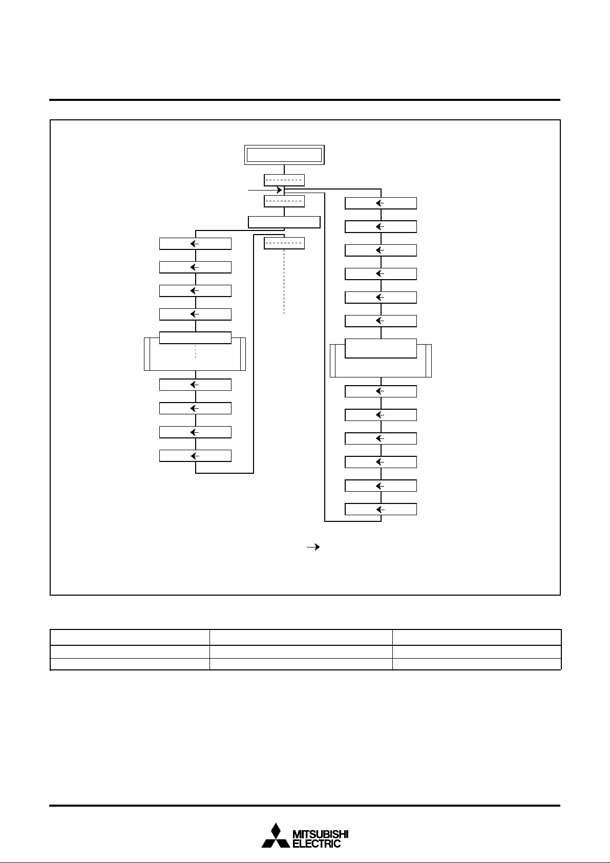
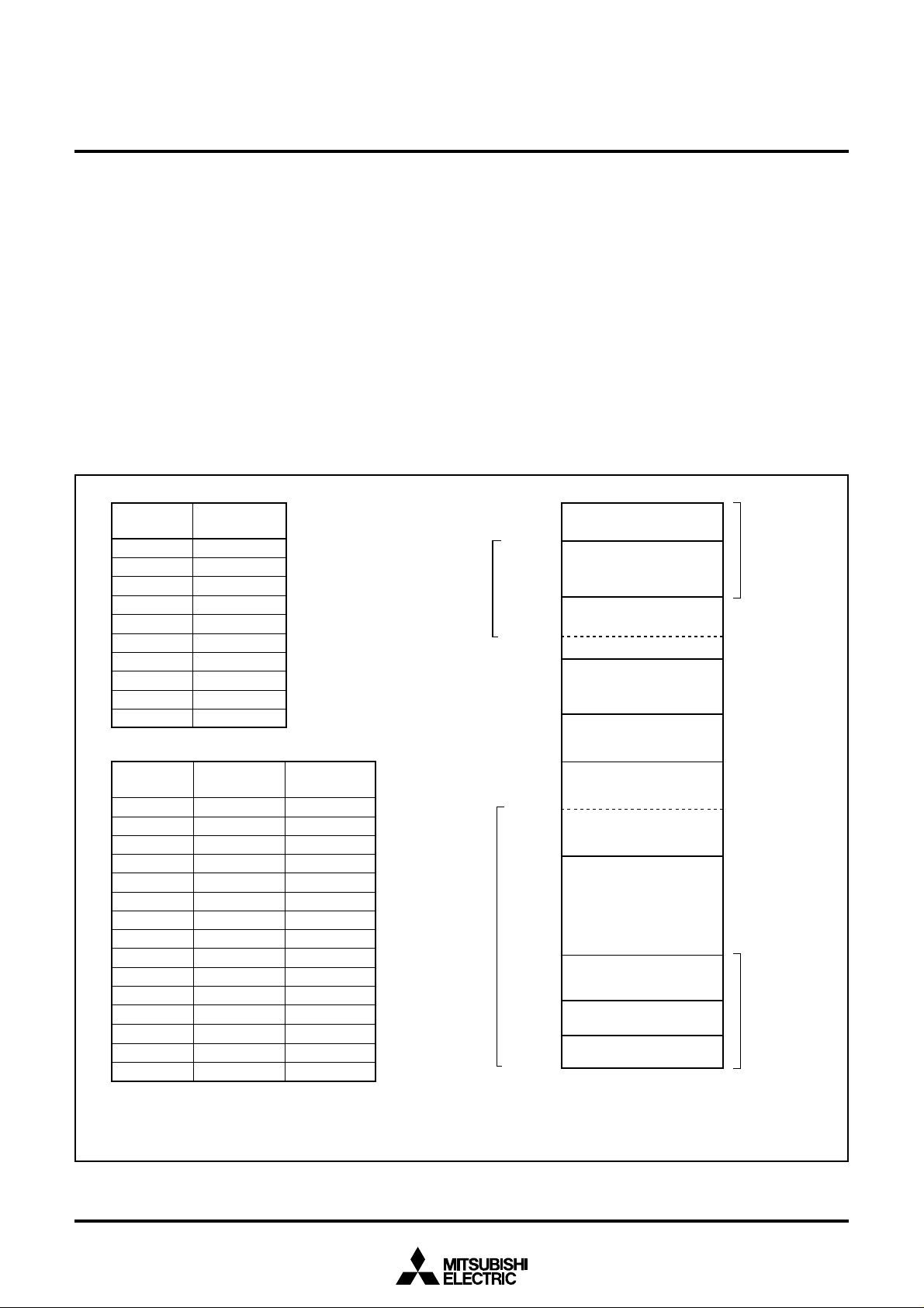
FUNCTIONAL BLOCK DIAGRAM (Package: 144P6Q-A)
Fig. 2 Functional block diagram
3
Page 4
PRELIMINARY
Notice: This is not a final specification.
Some parametric limits are subject to
change.
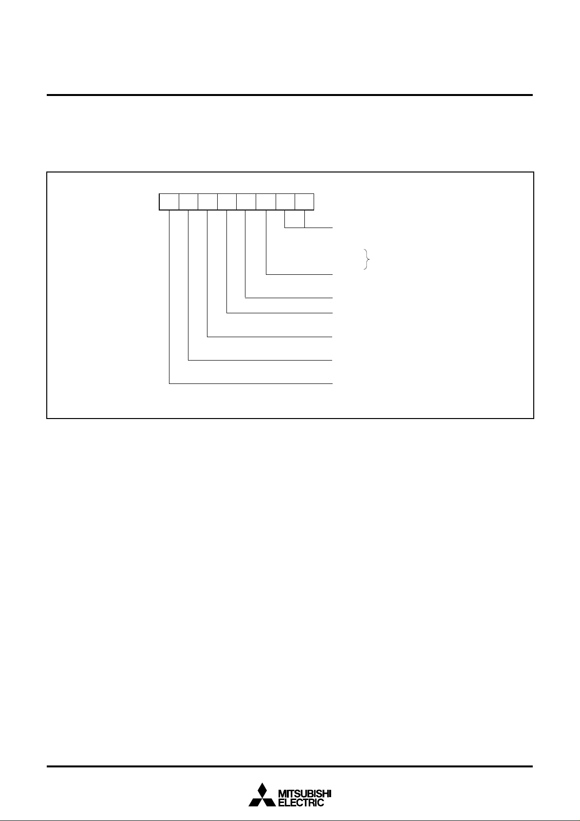
PIN DESCRIPTION
Table 1 Pin description
MITSUBISHI MICROCOMPUTERS
38C8 Group
SINGLE-CHIP 8-BIT CMOS MICROCOMPUTER
Pin
VCC, VSS
RESET
XIN
XOUT
OSCSEL
XCIN
XCOUT
VLIN
VL1 – VL5
COM0 –
COM32
SEG0/COM16–
SEG7/COM23,
SEG60COM31–
SEG67/COM
SEG8–SEG59
P00–P07
P14–P17
P10/AIN4–
P13/AIN7
P20–P27
P30/AIN0 –
P33/AIN3
P40/INT0
P41/INT1/ADT
P42/CNTR0/
BEEP+,
P43/CNTR1/
BEEP-
P44/RxD,
P45/TxD,
P46/SCLK,
P47/SRDY
C1,
C2,
C3
VSS (NC), NC
24
Name
Power source
Reset input
Clock input
Clock output
RC oscillation
select
Sub-clock input
Sub-clock output
Power source
input for LCD
LCD power
source
Common output
Segment output/
Common output
Segment output
I/O port P0
I/O port P1
I/O port P2
I/O port P3
Input port P4
I/O port P4
Voltage multiplier
Function
• Apply voltage of 4.0–5.5 V to VCC, and 0 V to VSS. (at high-speed mode)
• Reset input pin for active “L.”
• Input and output pins for the main clock generating circuit.
• Feedback resistor is built in between XIN pin and XOUT pin.
• Connect a ceramic resonator or a quartz-crystal oscillator between the XIN and XOUT pins to set the
oscillation frequency.
• If an external clock is used, connect the clock source to the XIN pin and leave the XOUT pin open.
• This pin determines the oscillation between XIN and XOUT. The oscillation method can be selected from
either by an oscillator or by a resistor.
• Input and output pins for sub-clock generating circuit. (Connect a quartz-crystal oscillator between the
XCIN and XCOUT pins to set the oscillation frequency . The clock generated the externals cannot be input
directly.)
• Reference voltage input pin for LCD.
• The input voltage to this pin is boosted threefold by voltage multiplier.
• LCD drive power source pins.
• LCD common output pins.
• LCD segment/common output pins.
• LCD segment output pins.
• 8-bit I/O port.
• CMOS compatible input level.
• CMOS 3-state output structure.
• 4-bit I/O port.
• CMOS compatible input level.
• CMOS 3-state output structure.
• 1-bit input port.
• CMOS compatible input level.
• 7-bit I/O port.
• CMOS compatible input level.
• CMOS 3-state output structure.
• I/O direction register allows each pin to be individually
programmed as either input or output.
• External capacitor connect pins for a voltage multiplier of LCD.
• Non-function pins.
• Leave the VSS (NC) pin open.
Function except a port function
• A-D converter analog input pin
• Key-on wake-up interrupt input pin
• A-D converter analog input pin
• External interrupt pin
• External interrupt pin
• A-D trigger input pin
•Timer function I/O pin
• Serial I/O I/O pin
4
Page 5
PRELIMINARY
M
M F
X X X F P
P
R O M / P R O M
The fi
ROM
M
RAM si
Pack
R O M
b
Notice: This is not a final specification.
Some parametric limits are subject to
change.
P ART NUMBERING
r o d u c
t
3 8 C
89
MITSUBISHI MICROCOMPUTERS
38C8 Group
SINGLE-CHIP 8-BIT CMOS MICROCOMPUTER
–
age type
FP: 144P6Q-A package
n u m b e
O m i t t e d i n O n e T i m e P R O M v e r s i o n .
s i z
1 : 4 0 9 6 b y t e s
2 : 8 1 9 2 b y t e s
3 : 1 2 2 8 8 b y t e s
4 : 1 6 3 8 4 b y t e s
5 : 2 0 4 8 0 b y t e s
6 : 2 4 5 7 6 b y t e s
7 : 2 8 6 7 2 b y t e s
8 : 3 2 7 6 8 b y t e s
are reserved areas; they cannot be used.
e m o r y t y p
M : M a s k R O M v e r s i o n
E : O n e T i m e P R O M v e r s i o n
r
e
y t e
9 : 3 6 8 6 4
A : 4 0 9 6 0 b y t e s
B : 4 5 0 5 6 b y t e s
C : 4 9 1 5 2 b y t e s
D : 5 3 2 4 8 b y t e s
E : 5 7 3 4 4 b y t e s
F : 6 1 4 4 0 b y t e s
rst 128 bytes and the last 2 bytes of
e
s
Fig. 3 Part numbering
ze
0: 192 bytes
1: 256 bytes
2: 384 bytes
3: 512 bytes
4: 640 bytes
5: 768 bytes
6: 896 bytes
7: 1024 bytes
8: 1536 bytes
9: 2048 bytes
5
Page 6
PRELIMINARY
Notice: This is not a final specification.
Some parametric limits are subject to
change.
MITSUBISHI MICROCOMPUTERS
38C8 Group
SINGLE-CHIP 8-BIT CMOS MICROCOMPUTER
GROUP EXPANSION
Mitsubishi plans to expand the 38C8 group as follows.
Memory Type
Support for mask ROM and One Time PROM versions
Memory Size
ROM/PROM size ............................................................ 60 K bytes
RAM size........................................................................ 2048 bytes
Memory Expansion Plan
R O M s i z e ( b y t e s )
6 0 K
56K
4 8 K
4 0 K
3 2 K
28K
24K
20K
Packages
144P6Q-A ...................................0.5 mm-pitch plastic molded QFP
U n d e r d e v e l o p m e n t
M38C89MF/EF
16K
1 2 K
8K
4K
2 5 63 8 45 1 2 640 7 6 88 9 6
192
P r o d u c t s u n d e r d e v e l o p m e n t o r p l a n n i n g : t h e d e v e l o p m e n t s c h e d u l e a n d s p e c i f i c a t i o n m a y b e r e v i s e d w i t h o u t
n o t i c e . T h e d e v e l o p m e n t o f p l a n n i n g p r o d u c t s m a y b e s t o p p e d .
Fig. 4 Memory expansion plan
Currently planning products are listed below.
Table 2 Support products
Product name
M38C89MF-XXXFP
M38C89EFFP
(P) ROM size (bytes)
ROM size for User in ( )
61440 (61310)
61440 (61310)
R A M s i z e ( b y t e s )
RAM size
(bytes)
2048
2048
1,024
Package
144P6Q-A
144P6Q-A
1 , 5 3 62
Remarks
Mask ROM version
One Time PROM version
, 0 4
8
As of Dec. 2000
6
Page 7
PRELIMINARY
Notice: This is not a final specification.
Some parametric limits are subject to
change.
MITSUBISHI MICROCOMPUTERS
38C8 Group
SINGLE-CHIP 8-BIT CMOS MICROCOMPUTER
FUNCTIONAL DESCRIPTION
CENTRAL PROCESSING UNIT (CPU)
The 38C8 group uses the standard 740 family instruction set. Refer
to the table of 740 family addressing modes and machine instructions or the 740 Family Software Manual for details on the instruction
set.
Machine-resident 740 family instructions are as follows:
The FST and SLW instruction cannot be used.
The STP, WIT, MUL, and DIV instruction can be used.
[Accumulator (A)]
The accumulator is an 8-bit register. Data operations such as data
transfer, etc., are executed mainly through the accumulator.
[Index Register X (X)]
The index register X is an 8-bit register. In the index addressing modes,
the value of the OPERAND is added to the contents of register X and
specifies the real address.
[Index Register Y (Y)]
The index register Y is an 8-bit register. In partial instruction, the
value of the OPERAND is added to the contents of register Y and
specifies the real address.
b7
[Stack Pointer (S)]
The stack pointer is an 8-bit register used during subroutine calls
and interrupts. This register indicates start address of stored area
(stack) for storing registers during subroutine calls and interrupts.
The low-order 8 bits of the stack address are determined by the contents of the stack pointer. The high-order 8 bits of the stack address
are determined by the stack page selection bit. If the stack page
selection bit is “0” , the high-order 8 bits becomes “0016”. If the stack
page selection bit is “1”, the high-order 8 bits becomes “0116”.
The operations of pushing register contents onto the stack and popping them from the stack are shown in Figure 6.
Store registers other than those described in Figure 6 with program
when the user needs them during interrupts or subroutine calls.
[Program Counter (PC)]
The program counter is a 16-bit counter consisting of two 8-bit registers PCH and PCL. It is used to indicate the address of the next instruction to be executed.
b0
A Accumulator
b7
b0
X Index register X
b7
b0
Y Index register Y
b7 b0
S Stack pointer
b7b15 b0
L Program counterPCH
PC
b7 b0
N V T B D I Z C Processor status register (PS)
Carry flag
Zero flag
Interrupt disable flag
Decimal mode flag
Break flag
Index X mode flag
Overflow flag
Negative flag
Fig. 5 740 Family CPU register structure
7
Page 8
PRELIMINARY
e
Notice: This is not a final specification.
Some parametric limits are subject to
change.
O n - g o i n g R o u t i n
MITSUBISHI MICROCOMPUTERS
38C8 Group
SINGLE-CHIP 8-BIT CMOS MICROCOMPUTER
P u s h r e t u r n a d d r e s s
o n s t a c k
POP return
address from stack
Interrupt request
M ( S )( P CH)
S ) –
( S )
M ( S )( P CL)
(S) (S)– 1
Subroutine
E x e c u t e R T S
S ) +
( S )
( P CL)M ( S )
(S) (S) + 1
( P CH)M ( S )
(Note)
(
(
M (S) (PCH)
E x e c u t e J S R
1
1
S ) –
( S )
(
1
M ( S )( P CL)
S ) –
( S )
(
1
M ( S )( P S )
S ) –
( S )
(
1
Interrupt
Service Routine
Execute RTI
S ) +
( S )
(
1
(PS) M (S)
S ) +
( S )
(
1
(PCL)M (S)
S ) +
( S )
(
1
Push return address
on stack
Push contents of processor
status register on stack
I Flag is set from “0” to “1”
Fetch the jump vector
POP contents of
processor status
register from stack
POP return
address
from stack
Note: Condition for acceptance of an interrupt Interrupt enable flag is “1”
Fig. 6 Register push and pop at interrupt generation and subroutine call
Table 3 Push and pop instructions of accumulator or processor status register
Push instruction to stack
Accumulator
Processor status register
I n t e r r u p t d i s a b l e f l a g i s “ 0 ”
PHA
PHP
(PCH)M (S)
Pop instruction from stack
PLA
PLP
8
Page 9
PRELIMINARY
Notice: This is not a final specification.
Some parametric limits are subject to
change.
MITSUBISHI MICROCOMPUTERS
38C8 Group
SINGLE-CHIP 8-BIT CMOS MICROCOMPUTER
[Processor status register (PS)]
The processor status register is an 8-bit register consisting of 5 flags
which indicate the status of the processor after an arithmetic operation and 3 flags which decide MCU operation. Branch operations can
be performed by testing the Carry (C) flag , Zero (Z) flag, Overflow
(V) flag, or the Negative (N) flag. In decimal mode, the Z, V, N flags
are not valid.
•Bit 0: Carry flag (C)
The C flag contains a carry or borrow generated by the arithmetic
logic unit (ALU) immediately after an arithmetic operation. It can
also be changed by a shift or rotate instruction.
•Bit 1: Zero flag (Z)
The Z flag is set if the result of an immediate arithmetic operation
or a data transfer is “0”, and cleared if the result is anything other
than “0”.
•Bit 2: Interrupt disable flag (I)
The I flag disables all interrupts except for the interrupt
generated by the BRK instruction.
Interrupts are disabled when the I flag is “1”.
•Bit 3: Decimal mode flag (D)
The D flag determines whether additions and subtractions are
executed in binary or decimal. Binary arithmetic is executed when
this flag is “0”; decimal arithmetic is executed when it is “1”.
Decimal correction is automatic in decimal mode. Only the ADC
•Bit 4: Break flag (B)
The B flag is used to indicate that the current interrupt was
generated by the BRK instruction. The BRK flag in the processor
status register is always “0”. When the BRK instruction is used to
generate an interrupt, the processor status register is pushed
onto the stack with the break flag set to “1”.
•Bit 5: Index X mode flag (T)
When the T flag is “0”, arithmetic operations are performed
between accumulator and memory. When the T flag is “1”, direct
arithmetic operations and direct data transfers are enabled
between memory locations.
•Bit 6: Overflow flag (V)
The V flag is used during the addition or subtraction of one byte
of signed data. It is set if the result exceeds +127 to -128. When
the BIT instruction is executed, bit 6 of the memory location
operated on by the BIT instruction is stored in the overflow flag.
•Bit 7: Negative flag (N)
The N flag is set if the result of an arithmetic operation or data
transfer is negative. When the BIT instruction is executed, bit 7 of
the memory location operated on by the BIT instruction is stored
in the negative flag.
Table 4 Set and clear instructions of each bit of processor status register
Set instruction
Clear instruction
C flag
SEC
CLC
Z flag
–
–
I flag
SEI
CLI
D flag
SED
CLD
B flag
–
–
T flag
SET
CLT
V flag
–
CLV
N flag
–
–
9
Page 10
PRELIMINARY
N
P
CPU
( C P U M
B
)
b
b
Notice: This is not a final specification.
Some parametric limits are subject to
change.
[CPU Mode Register (CPUM)] 003B16
The CPU mode register contains the stack page selection bit and the
internal system clock selection bit.
The CPU mode register is allocated at address 003B16.
MITSUBISHI MICROCOMPUTERS
38C8 Group
SINGLE-CHIP 8-BIT CMOS MICROCOMPUTER
7
Fig. 7 Structure of CPU mode register
0
mode register
( C M ) : a d d r e s s 0 0 3
rocessor mode bits
b1 b0
0 0 : Single-chip mode
0 1 :
1 0 :
1 1 :
Stack page selection bit
0 : 0 page
1 : 1 page
Not used (returns “1” when read)
(Do not write “0” to this bit)
Sub-clock (X
0 : Stopped
1 : Oscillating
Main clock (X
0 : Oscillating
1 : Stopped
Main clock division ratio selection bit
0 : f(X
1 : f(XIN)/8 (middle-s peed mode)
Internal system clock selection bit
0 : X
1 : XCIN–XCOUT selected (low-s peed mode)
o t a v a i l a b l
CIN–XCOUT) stop bit
IN–XOUT) stop bit
IN)/2 (high-speed m ode)
IN–XOUT selected (m iddle-/high-speed mode)
1 6
e
10
Page 11
PRELIMINARY
F F
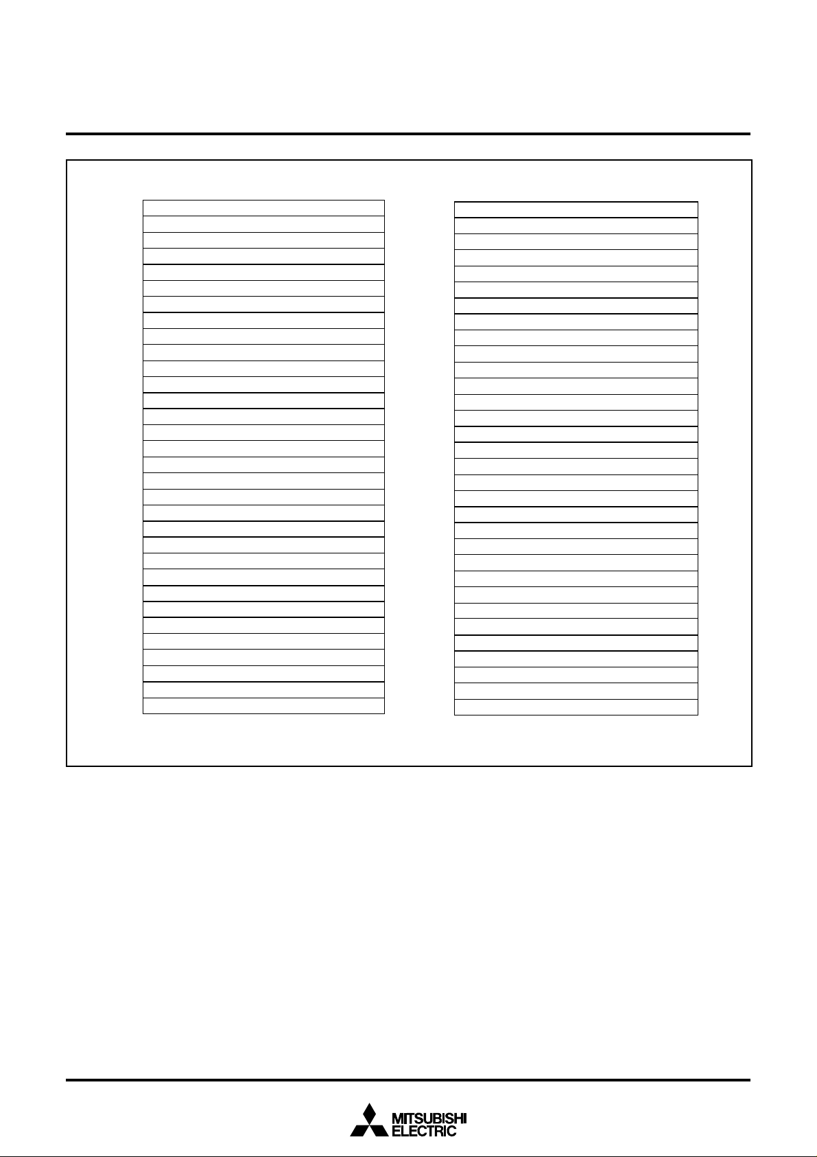
R A M
R A M
A d d
F
F
R O M
R O M
Add
Add
F F
F F D C
F F F E
FFFF16X X X X
YYYY16ZZZZ
RAM
ROM
S F R
N
d
I
a
R
Z
S
R
ROM
Notice: This is not a final specification.
Some parametric limits are subject to
change.
MITSUBISHI MICROCOMPUTERS
38C8 Group
SINGLE-CHIP 8-BIT CMOS MICROCOMPUTER
MEMORY
Special Function Register (SFR) Area
The Special Function Register area in the zero page contains control
Zero Page
Access to this area with only 2 bytes is possible in the zero page
addressing mode.
registers such as I/O ports and timers.
Special Page
RAM
RAM is used for data storage and for stack area of subroutine calls
and interrupts.
Access to this area with only 2 bytes is possible in the special page
addressing mode.
ROM
The first 128 bytes and the last 2 bytes of ROM are reserved for
device testing and the rest is user area for storing programs.
Interrupt Vector Area
The interrupt vector area contains reset and interrupt vectors.
a r e
a
s i z
( b y t e s )
192
256
384
512
640
768
896
1024
1536
2048
a r e
s i z
( b y t e s )
4 0 9 6
8 1 9 2
1 2 2 8 8
1 6 3 8 4
2 0 4 8 0
2 4 5 7 6
2 8 6 7 2
3 2 7 6 8
3 6 8 6 4
4 0 9 6 0
4 5 0 5 6
4 9 1 5 2
5 3 2 4 8
5 7 3 4 4
6 1 4 4 0
r e s s
e
X X X X
0 0
0 1 3 F
0 1 B F
0 2 3 F
0 2 B F
0 3 3 F
0 3 B F
0 4 3 F
0 6 3 F
0 8 3 F
1 6
1 6
1 6
1 6
1 6
1 6
1 6
1 6
1 6
1 6
1 6
a
e
YYYY
0 0
E 0 0 0
D 0 0 0
C 0 0 0
B 0 0 0
A 0 0 0
9 0 0 0
8 0 0 0
7 0 0 0
6 0 0 0
5 0 0 0
4 0 0 0
3 0 0 0
20 0 0
10 0 0
ress
0
16
1 6
1 6
1 6
1 6
1 6
1 6
1 6
1 6
1 6
1 6
1 6
1 6
1 6
1 6
1 6
ZZZZ
080
E080
D080
C080
B080
A080
9080
8080
7080
6080
5080
4080
3080
2080
1080
ress
16
16
16
16
16
16
16
16
16
16
16
16
16
16
16
16
0000
0040
0130
0 3 4 0
0 4 3 0
0840
0
16
16
LCD display RA M area
16
1 6
1 6
L C D d i s p l a y R A M a r e a
1 6
16
e s e r v e d R O M a r e
16
1 6
0
1 6
nterrupt vector are
1 6
eserved
a r e
ot use
( 1 2 8 b y t e s )
a
e r o p a g
e
✽
✽
a
p e c i a l p a g
e
area
✽ The stard address of the LCD display area can be switched either zero page (addresses 004016–00EF16) or 3 page (addresses
0340
16
Fig. 8 Memory map diagram
–03EF16) by software. Immediately after reset released, 3 page is selected.
11
Page 12
PRELIMINARY
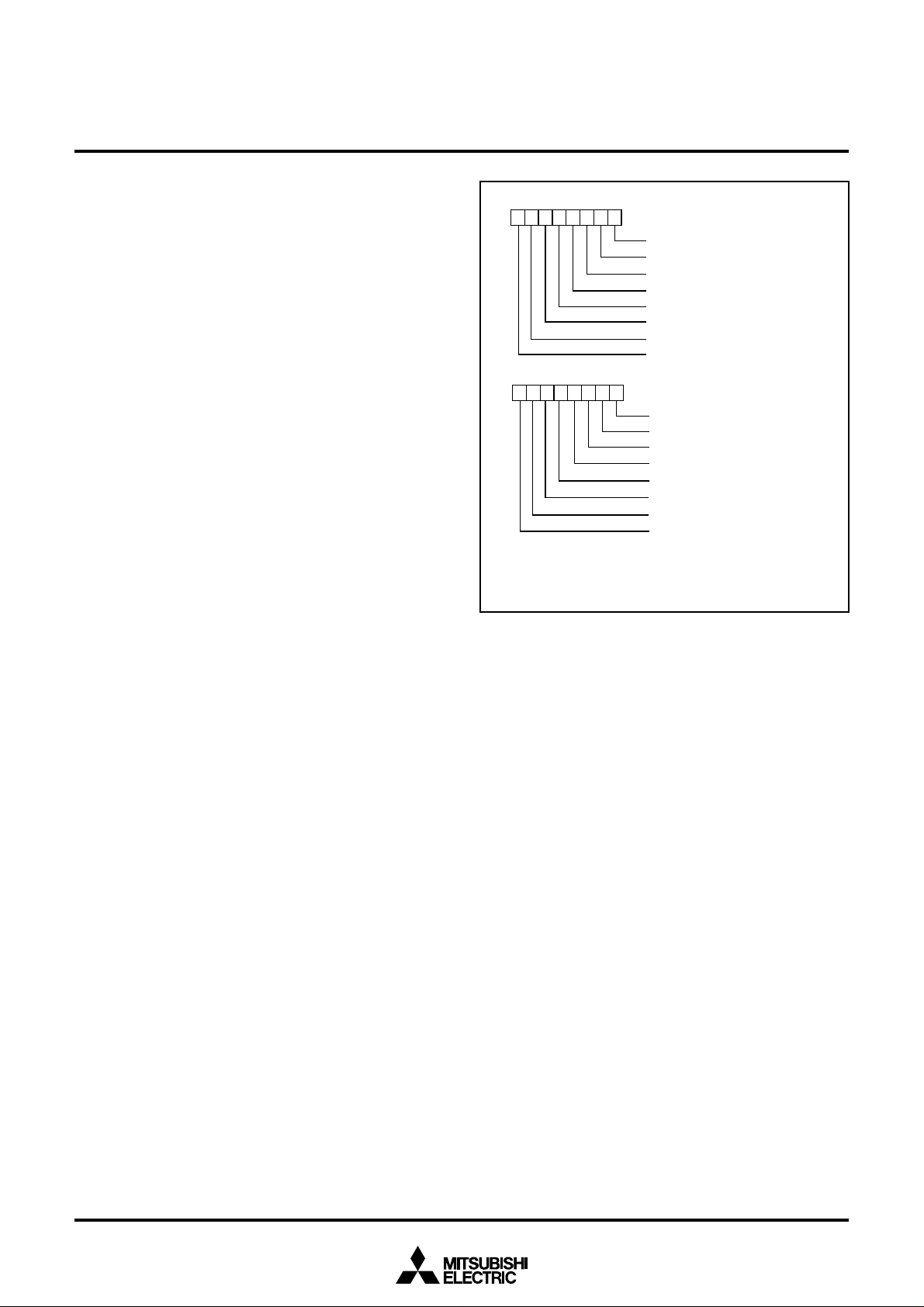
T
(TB/RB)
A
B
C
D
E
F
A
B
C
D
E
F
A
B
C
D
E
F
A
B
C
D
E
F
P
)
P
)
P
)
P
)
P
)
P
)
P
)
P
)
P
D)
S
)
Serial I/O
(SIOCON)
UART
(UARTCON)
I
)
Ti
(TXM)
I
(INTEDGE)
CPU
(CPUM)
I
(IREQ1)
I
(IREQ2)
I
(ICON1)
Ti
(TXL)
P U L L
)
P U L L
)
L C D
)
A
)
A-D
(ADL)
A-D
(high
(ADH)
P
)
B
)
T i
)
T i
)
T i
)
T i
)
T i
)
T i
)
T i
)
T i
)
L C D
)
L C D
)
Notice: This is not a final specification.
Some parametric limits are subject to
change.
0 0 0 0
1 6
ort P0 (P0
o r t P 0 d i r e c t i o n r e g i s t e r ( P 0 D
0 0 0 1
1 6
o r t P 1 ( P 1
0 0 0 2
1 6
o r t P 1 d i r e c t i o n r e g i s t e r ( P 1 D
0 0 0 3
1 6
0 0 0 4
1 6
ort P2 (P2
o r t P 2 d i r e c t i o n r e g i s t e r ( P 2 D
0 0 0 5
1 6
o r t P 3 ( P 3
0 0 0 6
1 6
o r t P 3 d i r e c t i o n r e g i s t e r ( P 3 D
0 0 0 7
1 6
o r t P 4 ( P 4
0 0 0 8
1 6
0009
16
ort P4 direction register (P4
000
16
0 0 0
1 6
0 0 0
1 6
0 0 0
1 6
0 0 0
1 6
0 0 0
1 6
0010
16
0 0 1 1
1 6
0012
16
0013
16
0 0 1 4
1 6
0 0 1 5
1 6
r e g i s t e r A ( P U L L A
0 0 1 6
1 6
r e g i s t e r B ( P U L L B
0 0 1 7
1 6
0 0 1 8
1 6
ransmit/Receive buffer register
e r i a l I / O s t a t u s r e g i s t e r ( S I O S T S
0019
16
001
001
001
001
001
001
16
16
a u d r a t e g e n e r a t o r ( B R G
16
16
16
16
control register
control register
0020
0021
0022
0023
0024
0025
0026
0027
0028
0029
0 0 2
0 0 2
002
002
002
002
0030
0031
0032
0033
0034
0035
0036
0037
0038
0039
0 0 3
0 0 3
0 0 3
0 0 3
0 0 3
003
MITSUBISHI MICROCOMPUTERS
38C8 Group
SINGLE-CHIP 8-BIT CMOS MICROCOMPUTER
16
mer X (low-order)
m e r X ( h i g h - o r d e r ) ( T X H
16
m e r Y ( l o w - o r d e r ) ( T Y L
16
m e r Y ( h i g h - o r d e r ) ( T Y H
16
m e r 1 ( T 1
16
m e r 2 ( T 2
16
m e r 3 ( T 3
16
16
mer X mode register
m e r Y m o d e r e g i s t e r ( T Y M
16
m e r 1 2 3 m o d e r e g i s t e r ( T 1 2 3 M
16
1 6
1 6
16
16
16
16
16
- D c o n t r o l r e g i s t e r ( A D C O N
16
16
conversion register (low-order)
16
conversion register
16
16
16
c o n t r o l r e g i s t e r 1 ( L C 1
16
c o n t r o l r e g i s t e r 2 ( L C 2
16
m o d e r e g i s t e r ( L M
16
1 6
nterrupt edge selection register
1 6
mode register
1 6
nterrupt request register 1
1 6
nterrupt request register 2
1 6
nterrupt control register 1
n t e r r u p t c o n t r o l r e g i s t e r 2 ( I C O N 2
16
-order)
Fig. 9 Memory map of special function register (SFR)
12
Page 13
PRELIMINARY
P 00– P 03 p u l l - u p
P 04– P 07 p u l l - u p
P 1
0
– P 13 p u l l - u p
P 14– P 17 p u l l - u p
P 20– P 23 p u l l - u p
P 24– P 27 p u l l - u p
P 3
0
– P 33 p u l l - u p
N o t u s e d ( r e t u r n “ 0 ” w h e n r e a d )
N o t e : T h e c o n t e n t s o f P U L L r e g i s t e r A a n d P U L L r e g i s t e r B d o
n o t a f f e c t p o r t s p r o g r a m m e d a s t h e o u t p u t p o r t .
Notice: This is not a final specification.
Some parametric limits are subject to
change.
MITSUBISHI MICROCOMPUTERS
38C8 Group
SINGLE-CHIP 8-BIT CMOS MICROCOMPUTER
I/O PORTS
[Direction Registers]
The I/O ports P0–P3 and P41–P47 have direction registers which
determine the input/output direction of each individual pin. Each bit
in a direction register corresponds to one pin, each pin can be set to
be input port or output port.
When “0” is written to the bit corresponding to a pin, that pin becomes an input pin. When “1” is written to that bit, that pin becomes
an output pin.
If data is read from a pin set to output, the value of the port output
latch is read, not the value of the pin itself. Pins set to input are floating. If a pin set to input is written to, only the port output latch is
written to and the pin remains floating.
Pull-up Control
By setting the PULL register A (address 001616) or the PULL register
B (address 001716), ports P0 to P4 except for port P40 can control
pull-up with a program.
However, the contents of PULL register A and PULL register B do not
affect ports programmed as the output ports.
b7 b0
b 7b0
PULL register A
(PULLA: address 0016
PULL register B
(PULLB: address 0017
N o t u s e d ( r e t u r n “ 0 ” w h e n r e a d )
P 41 p u l l - u p
P 4
2
p u l l - u p
P 43 p u l l - u p
P 4
4
p u l l - u p
P 45 p u l l - u p
P 46 p u l l - u p
P 4
7
p u l l - u p
16
16
0: No pull-up
1: Pull-up
)
)
Fig. 10 Structure of PULL register A and PULL register B
13
Page 14
PRELIMINARY
Notice: This is not a final specification.
Some parametric limits are subject to
change.
Table 5 List of I/O port function
Pin
P00–P07
P10/AN4–
P13/AN7
P14–P17
P20–P27
P30/AN0–
P33/AN3
P40/INT0
P41/INT1
P42/CNTR0/
BEEP+
P43/CNTR1/
BEEPP44/RxD
P45/TxD
P46/SCLK
P47/SRDY
COM0–COM7,
COM8–COM
SEG0/COM16–
SEG7/COM23,
SEG60/COM31–
SEG67/COM
SEG8–SEG
24
59
Name
Port P0
Port P1
Port P2
Port P3
Port P4
Common
15
Segment/
Common
Segment
Input/Output
Input/Output,
individual bits
Input/Output,
individual bits
Input/Output,
individual bits
Input
Input/Output,
individual bits
Output
I/O format
CMOS 3-state output
CMOS compatible input
level
CMOS 3-state output
CMOS 3-state output
CMOS compatible input
level
CMOS compatible input
level
CMOS 3-state output
LCD common output
LCD segment output
LCD common ouput
LCD segment output
MITSUBISHI MICROCOMPUTERS
38C8 Group
SINGLE-CHIP 8-BIT CMOS MICROCOMPUTER
Non-port function
Key input (key-on
wake-up) interrupt input
A-D converter input
External interrupt input
Timer X function I/O
Timer Y function input
Serial I/O funtion
I/O
Related SFRs
PULL register A
PULL register A
A-D control register
PULL register A
PULL register A
Interrupt control register 2
PULL register A
A-D control register
PULL register B
Interrupt edge select
register
PULL register B
Timer X mode register
PULL register B
Timer Y mode register
PULL register B
Serial I/O control register
Serial I/O status register
UART control register
LCD mode register
Ref. No.
(1)
(2)
(1)
(1)
(2)
(3)
(1)
(4)
(5)
(6)
(7)
(8)
(9)
14
Page 15
PRELIMINARY
Notice: This is not a final specification.
Some parametric limits are subject to
change.
MITSUBISHI MICROCOMPUTERS
38C8 Group
SINGLE-CHIP 8-BIT CMOS MICROCOMPUTER
( 1 ) P o r t s P 0 , P 14– P 17, P 2 , P 4
D i r e c t i o n
r e g i s t e r
D a t a b u s
P o r t l a t c h
K e y - o n w a k e - u p i n t e r r u p t i n p u t
1
i n t e r r u p t i n p u t , A D T
I N T
1
P u l l - u p c o n t r o l
E x c e p t P 0 , P 1
(3) Port P4
INT0 interrupt input
0
D a t a b u s
( 2 ) P o r ts P 10– P 13, P 3
D i r e c t i o n
r e g i s t e r
Data bus
Port latch
P u l l - u p c o n t r o l
A-D converter input
A n a l o g i n p u t p i n s e l e c t i o n b i t
( 4 ) P o r t P 4
D a t a b u s
2
D i r e c t i o n
r e g i s t e r
P o r t l a t c h
B u z z e r o u t p u t m o d e
T i m e r o u t p u t
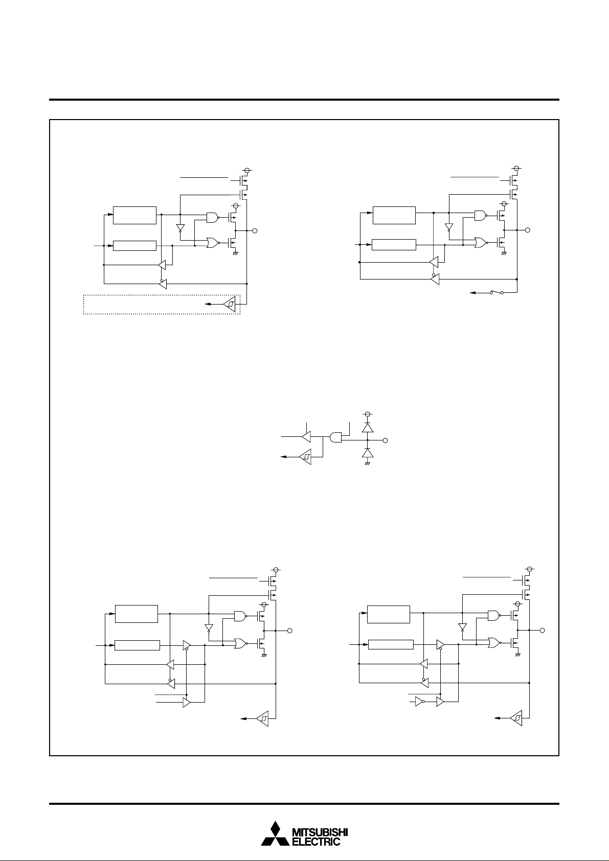
Fig. 11 Port block diagram (1)
P u l l - u p c o n t r o l
C N T R0 i n t e r r u p t i n p u t
( 5 ) P o r t P 4
Data bus
Buzzer output mode
3
Direction
register
P o r t l a t c h
Timer output
CNTR
Pull-up control
1
interrupt input
15
Page 16
PRELIMINARY
t
t
t
s
t
t
t
t
t
t
t
Notice: This is not a final specification.
Some parametric limits are subject to
change.
MITSUBISHI MICROCOMPUTERS
38C8 Group
SINGLE-CHIP 8-BIT CMOS MICROCOMPUTER
( 6 ) P o r t P 4
D a t a b u s
(8) Port P4
S e r i a l I / O s y n c h r o n o u
4
S e r i a l I / O e n a b l e b i
R e c e i v e e n a l b l e b i
D i r e c t i o n
r e g i s t e r
P o r t l a t c h
6
c l o c k s e l e c t i o n b i
S e r i a l I / O e n a b l e b i t
Serial I/O mode selection bi
Serial I/O enable bi
Direction
register
Pull-up control
S e r i a l I / O i n p u t
Pull-up control
( 7 ) P o r t P 4
P45/TxD P-channel output disable bit
D a t a b u s
(9) Port P4
S e r i a l I / O m o d e s e l e c t i o n b i
5
S e r i a l I / O e n a b l e b i
T r a n s m i t e n a b l e b i
Direction
register
P o r t l a t c h
Serial I/O output
7
S e r i a l I / O e n a b l e b i
S
R D Y
o u t p u t e n a b l e b i
Direction
register
Pull-up control
P u l l - u p c o n t r o l
Port latchData bus
Serial I/O clock output
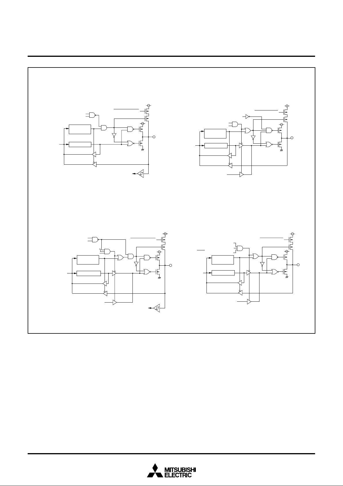
Fig. 12 Port block diagram (2)
Serial I/O clock input
Data bus
Serial I/O ready output
P o r t l a t c h
16
Page 17

PRELIMINARY
Notice: This is not a final specification.
Some parametric limits are subject to
change.
MITSUBISHI MICROCOMPUTERS
38C8 Group
SINGLE-CHIP 8-BIT CMOS MICROCOMPUTER
INTERRUPTS
Interrupts occur by fifteen sources: six external, eight internal, and
one software.
Interrupt Control
Each interrupt except the BRK instruction interrupt have both an interrupt request bit and an interrupt enable bit, and is controlled by the
interrupt disable flag. An interrupt occurs if the corresponding interrupt request and enable bits are “1” and the interrupt disable flag is
“0”.
Interrupt enable bits can be set or cleared by software. Interrupt request bits can be cleared by software, but cannot be set by software.
The BRK instruction interrupt and reset cannot be disabled with any
flag or bit. The I flag disables all interrupts except the BRK instruction
interrupt and reset. If several interrupts requests occurs at the same
time the interrupt with highest priority is accepted first.
Table 6 Interrupt vector addresses and priority
Interrupt Source
Reset (Note 2)
INT0
INT1
Serial I/O
reception
Serial I/O
transmission
Timer X
Timer Y
Timer 2
Timer 3
CNTR0
CNTR1
Timer 1
Key input (Key-
on wake-up)
A-D conversion
BRK instruction
Notes 1: Vector addresses contain interrupt jump destination addresses.
2: Reset function in the same way as an interrupt with the highest priority.
Priority
Vector Addresses (Note 1)
High
1
FFFD16
2
FFFB16
3
FFF916
4
FFF716
5
FFF516
6
FFF316
7
FFF116
8
FFEF16
9
FFED16
10
11
12
13
14
15
FFEB16
FFE916
FFE716
FFE116
FFDF16
FFDD16
Low
FFFC16
FFFA16
FFF816
FFF616
FFF416
FFF216
FFF016
FFEE16
FFEC16
FFEA16
FFE816
FFE616
FFE016
FFDE16
FFDC16
At reset
At detection of either rising or falling edge of
INT0 intput
At detection of either rising or falling edge of
INT1 input
At completion of serial I/O data reception
At completion of serial I/O transmission shift
or when transmission buffer is empty
At timer X underflow
At timer Y underflow
At timer 2 underflow
At timer 3 underflow
At detection of either rising or falling edge of
CNTR0 input
At detection of either rising or falling edge of
CNTR1 input
At timer 1 underflow
At falling of port P2 (at input) input logical level
AND
At completion of A-D conversion
At BRK instruction execution
Interrupt Operation
By acceptance of an interrupt, the following operations are automatically performed:
1.The processing being executed is stopped.
2.The contents of the program counter and processor status register are automatically pushed onto the stack.
3.The interrupt disable flag is set and the corresponding interrupt
request bit is cleared.
4.The interrupt jump destination address is read from the vector
table into the program counter.
■Notes on interrupts
When setting the followings, the interrupt request bit may be set to
“1”.
•When setting external interrupt active edge
Related register: Interrupt edge selection register (address 3A16)
Timer X mode register (address 2716)
Timer Y mode register (address 2816)
•When switching interrupt sources of an interrupt vector address
where two or more interrupt sources are allocated
Related register: AD control regsiter (address 3116)
When not requiring for the interrupt occurrence synchronized with
these setting, take the following sequence.
➀Set the corresponding interrupt enable bit to “0” (disabled).
➁Set the interrupt edge select bit (active edge switch bit) or the inter-
rupt source select bit to “1”.
➂Set the corresponding interrupt request bit to “0” after 1 or more
instructions have been executed.
➃Set the corresponding interrupt enable bit to “1” (enabled).
Interrupt Request
Generating Conditions
Non-maskable
External interrupt
(active edge selectable)
External interrupt
(active edge selectable)
Valid when serial I/O is selected
Valid when serial I/O is selected
External interrupt
(active edge selectable)
External interrupt
(active edge selectable)
External interrupt
(falling valid)
Valid when A-D conversion interrupt
is selected
Non-maskable software interrupt
Remarks
17
Page 18

PRELIMINARY
t
t
t
I
I N T
i
d
( I R E Q
C
)
I
CNTR0 i
(IREQ
D16)
b7b
I
I N T
i
(INTEDGE
A16)
F
b7b0b
b
I
I N T
i
( I C O N
E
)
I
C N T R
i
d
( I C O N
F
)
b7b0b7b
Notice: This is not a final specification.
Some parametric limits are subject to
change.
I n t e r r u p t r e q u e s t b i
I n t e r r u p t e n a b l e b i
I n t e r r u p t d i s a b l e f l a g ( I )
MITSUBISHI MICROCOMPUTERS
38C8 Group
SINGLE-CHIP 8-BIT CMOS MICROCOMPUTER
Fig. 13 Interrupt control
0
n t e r r u p t e d g e s e l e c t i o n r e g i s t e
: address 003
n t e r r u p t e d g e s e l e c t i o n b i
0
I N T1 i n t e r r u p t e d g e s e l e c t i o n b i t
N o t u s e d ( r e t u r n “ 0 ” w h e n r e a d )
n t e r r u p t r e q u e s t r e g i s t e r
1 : a d d r e s s 0 0 3
n t e r r u p t r e q u e s t b i
0
I N T1 i n t e r r u p t r e q u e s t b i t
S e r i a l I / O r e c e i v e i n t e r r u p t r e q u e s t b i t
S e r i a l I / O t r a n s m i t i n t e r r u p t r e q u e s t b i t
T i m e r X i n t e r r u p t r e q u e s t b i t
T i m e r Y i n t e r r u p t r e q u e s t b i t
T i m e r 2 i n t e r r u p t r e q u e s t b i t
T i m e r 3 i n t e r r u p t r e q u e s t b i t
nterrupt control register 1
1 : a d d r e s s 0 0 3
n t e r r u p t e n a b l e b i
0
I N T1 i n t e r r u p t e n a b l e b i t
S e r i a l I / O r e c e i v e i n t e r r u p t e n a b l e b i t
S e r i a l I / O t r a n s m i t i n t e r r u p t e n a b l e b i t
T i m e r X i n t e r r u p t e n a b l e b i t
T i m e r Y i n t e r r u p t e n a b l e b i t
T i m e r 2 i n t e r r u p t e n a b l e b i t
T i m e r 3 i n t e r r u p t e n a b l e b i t
B R K i n s t r u c t i o n
r
1
1 6
t
1 6
t
R e s e
t
a l l i n g e d g e a c t i v
0 :
1 : R i s i n g e d g e a c t i v e
I n t e r r u p t r e q u e s t
e
7
n t e r r u p t r e q u e s t r e g i s t e r
0
2 : address 003
nterrupt request bit
CNTR
1 interrupt request bit
Timer 1 interrupt request bit
Not used (returns “0” when read)
Key input interrupt request bit
AD conversion interrupt request bit
Not used (returns “0” when read)
0 : No interrupt re quest issue
1 : Interrupt request issued
0
nterrupt control register 2
2 : a d d r e s s 0 0 3
n t e r r u p t e n a b l e b i
0
C N T R1 i n t e r r u p t e n a b l e b i t
T i m e r 1 i n t e r r u p t e n a b l e b i t
N o t u s e d ( r e t u r n s “ 0 ” w h e n r e a d )
( D o n o t w r i t e “ 1 ” t o t h i s b i t )
K e y i n p u t i n t e r r u p t e n a b l e b i t
A D c o n v e r s i o n i n t e r r u p t e n a b l e b i t
N o t u s e d ( r e t u r n s “ 0 ” w h e n r e a d )
( D o n o t w r i t e “ 1 ” t o t h i s b i t )
0 : Interrupts disable
1 : Interrupts enabled
2
1 6
t
Fig. 14 Structure of interrupt-related registers
18
Page 19

PRELIMINARY
Notice: This is not a final specification.
Some parametric limits are subject to
change.
MITSUBISHI MICROCOMPUTERS
38C8 Group
SINGLE-CHIP 8-BIT CMOS MICROCOMPUTER
Key Input Interrupt (Key-on Wake-Up)
A key input interrupt request is generated by applying “L” level to any
pin of port P2 that have been set to input mode. In other words, it is
generated when AND of input level goes from “1” to “0”. An example
P o r t P X x
“ L ” l e v e l o u t p u t
7
o u t p u t
P 2
6
output
P2
5
output
P2
4
output
P2
P U L L r e g i s t e r A
B i t 2 = “ 1 ”
✽
✽
✽
✽
Key input control register = “1”
7
d i r e c t i o n
P o r t P 2
r e g i s t e r = “ 1 ”
✽✽
Port P2
latch
Key input control register = “1”
P o r t P 2
6
d i r e c t i o n
r e g i s t e r = “ 1 ”
✽✽
Port P2
latch
K e y i n p u t c o n t r o l r e g i s t e r = “ 1 ”
P o r t P 2
5
d i r e c t i o n
r e g i s t e r = “ 1 ”
✽✽
Port P2
latch
Key input control register = “1”
Port P2
4
direction
register = “1”
✽✽
Port P2
latch
of using a key input interrupt is shown in Figure 15, where an interrupt request is generated by pressing one of the keys consisted as
an active-low key matrix which inputs to ports P20–P23.
Key input interrupt request
7
6
5
4
P 2
P2
P 2
P 2
3
i n p u t
2
i n p u t
1
input
0
i n p u t
Key input control register = “1”
Port P2
3
direction
✽
✽
✽
✽
register = “0”
✽✽
Port P2
✽✽
Port P2
✽✽
P o r t P 2
✽✽
3
Port P2
latch
K e y i n p u t c o n t r o l r e g i s t e r = “ 1 ”
2
direction
register = “0”
2
Port P2
latch
Key input control register = “1”
1
direction
register = “0”
1
Port P2
latch
K e y i n p u t c o n t r o l r e g i s t e r = “ 1 ”
0
d i r e c t i o n
r e g i s t e r = “ 0 ”
Port P2
0
latch
✽
P-channel transistor for pull-up
✽✽
CMOS output buffer
Port P2
Input reading circ uit
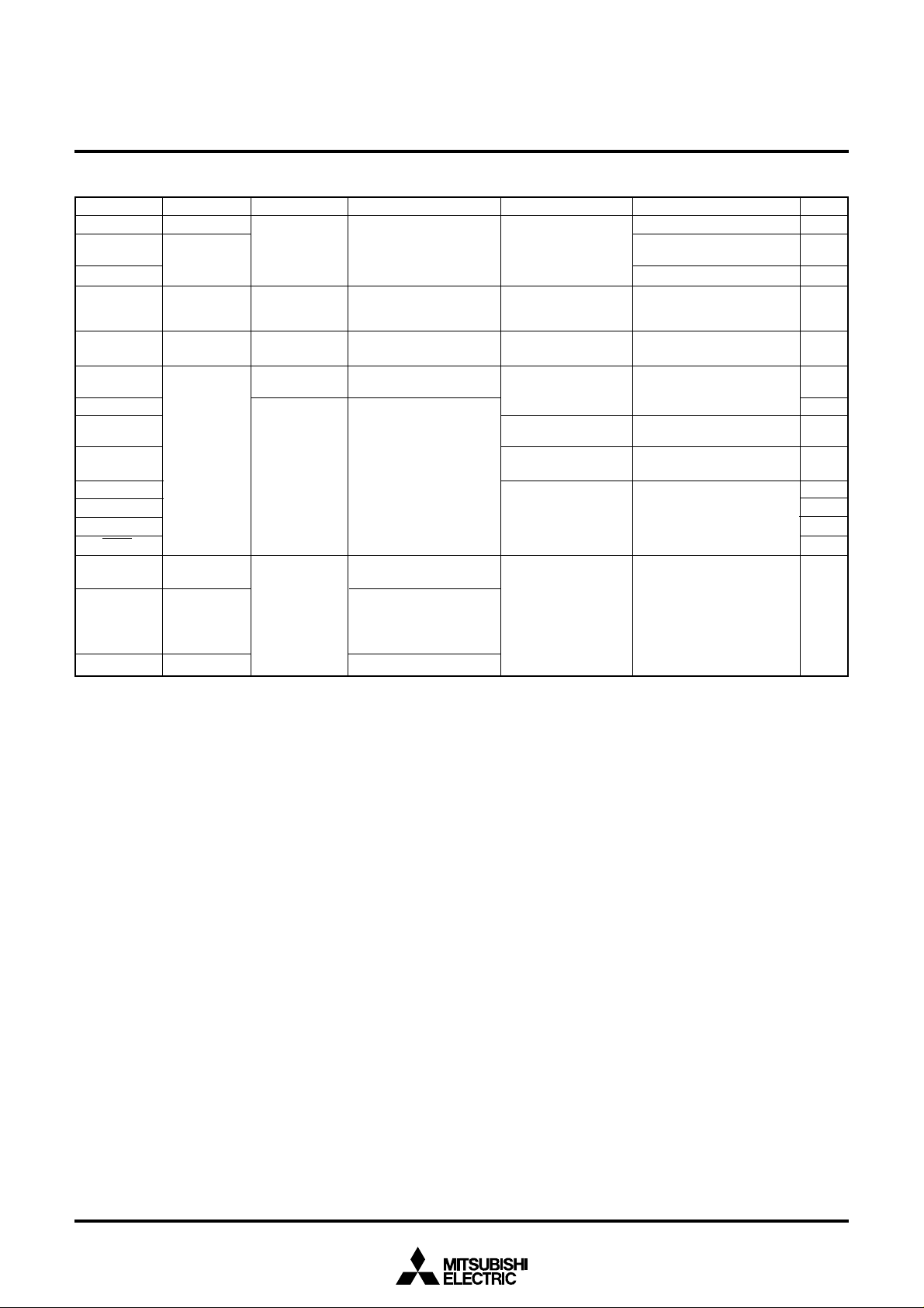
Fig. 15 Connection example when using key input interrupt and port P2 block diagram
19
Page 20

PRELIMINARY
Notice: This is not a final specification.
Some parametric limits are subject to
change.
MITSUBISHI MICROCOMPUTERS
38C8 Group
SINGLE-CHIP 8-BIT CMOS MICROCOMPUTER
TIMERS
The 38C8 group has five timers: timer X, timer Y, timer 1, timer 2, and
timer 3. Timer X and timer Y are 16-bit timers, and timer 1, timer 2,
and timer 3 are 8-bit timers.
All timers are down count timers. When the timer reaches “0016”, an
underflow occurs at the next count pulse and the corresponding timer
latch is reloaded into the timer and the count is continued. When a
timer underflows, the interrupt request bit corresponding to that timer
f ( X
I N
) / 1 6
( f ( X
C I N
) / 1 6 i n l o w - s p e e d m o d e✽)
P 42/ C N T R0/ B E E P +
P 42 d i r e c t i o n r e g i s t e r
P 43/ C N T R1/ B E E P -
f(X
CIN
)
Timer X operating
mode bits
CNTR1 active
edge switch bit
f ( X
“ 0 0 ” , “ 1 1 ”
“01”
C N T R0 a c t i v e
e d g e s w i t c h b i t
“ 0 ”
“ 1 ”
Pulse width
measurement
mode
B u z z e r o u t p u t m o d e
“0”
“ 1 ”
I N
)
T i m e r X c o u n t s o u r c e
s e l e c t i o n b i t
“ 1 ”
“ 0 ”
C N T R0 a c t i v e
e d g e s w i t c h b i t
2
latch
P4
Timer X operating
mode bits
“00”,“01”,“11”
“ 1 0 ”
“0”
“ 1 ”
IN
)/16
f(X
(f(X
CIN
)/16 in low-speed mode✽)
“00”,“01”,“11”
Timer Y operating
“10”
mode bits
Timer X stop con t ro l bit
S
Q
T
Q
Timer Y stop
control bit
is set to “1”.
Read and write operation on 16-bit timer must be performed for both
high and low-order bytes. When reading a 16-bit timer, read the highorder byte first. When writing to a 16-bit timer, write the low-order
byte first. The 16-bit timer cannot perform the correct operation when
reading during the write operation, or when writing during the read
operation.
Data bus
Timer X write control bit
T i m e r X ( l o w ) l a t c h ( 8 )
Timer X (low) (8) T i m e r X ( h i g h ) ( 8 )
P u l s e o u t p u t m o d e
Rising edge detection
Falling edge detection
T i m e r Y ( l o w ) l a t c h ( 8 ) Timer Y (low) high (8)
T i m e r Y ( l o w ) ( 8 ) Timer Y (high) (8)
T i m e r X ( h i g h ) l a t c h ( 8 )
Timer Y operating mode bits
Pulse width HL continuously
measurement mode
Period measu r ement mode
“ 0 0 ” , “ 0 1 ” , “ 1 0 ”
“11”
T i m e r Y i n t e r r u p t
r e q u e s t
T i m e r X i n t e r r u p t
r e q u e s t
C N T R 0 i n t e r r u p t
r e q u e s t
CNTR1 interrupt
request
P 4
3
d i r e c t i o n r e g i s t e r
f(XIN)/16
(f(X
CIN
)/16 in low-speed mode✽)
✽ I n t e r n a l c l o c k φ = X
Fig. 16 Timer block diagram
20
BEEP- valid bit
Timer 1 count source
selection bit
C I N
f ( X
P4
3
latch
“0”
T i m e r 1 l a t c h ( 8 )
) / 3 2
“1”
C I N
d i v i d e d b y 2 i n l o w - s p e e d m o d e
Timer 1 (8)
f ( X
C I N
f ( X
( f ( X
) / 3 2
Timer 3 count source
selection bit
T i m e r 2 c o u n t s o u r c e
s e l e c t i o n b i t
“ 0 ”
“ 1 ”
I N
) / 1 6
C I N
) / 1 6 i n l o w - s p e e d m o d e✽)
Timer 3 latch (8)
“ 0 ”
“1”
T i m e r 3 ( 8 )
T i m e r 2 l a t c h ( 8 )
Timer 2 (8)
Timer 2 write control bit
T i m e r 1 i n t e r r u p t
r e q u e s t
T i m e r 2 i n t e r r u p t
r e q u e s t
T i m e r 3 i n t e r r u p t
r e q u e s t
Page 21

PRELIMINARY
T i
T i
b
b
Notice: This is not a final specification.
Some parametric limits are subject to
change.
Timer X
Timer X is a 16-bit timer that can be selected in one of four modes
and can be controlled the timer X write by setting the timer X mode
register.
(1) Timer Mode
When the timer X count source selection bit is “0”, the timer counts
f(XIN)/16 (or f(XCIN)/16 in low-speed mode). When it is “1”, the timer
counts f(XIN).
(2) Buzzer Output Mode
Each time the timer underflows, a signal output from the BEEP+ pin
is inverted. When the BEEP- valid bit is “1”, the opposite phase of
BEEP+ signal is output from the BEEP- pin. When using the BEEP+
pin and the BEEP- pin, set ports shared with these pins to output.
(3) Event Counter Mode
The timer counts signals input through the CNTR0 pin.
Except for this, the operation in event counter mode is the same as
in timer mode. When using a timer in this mode, set the port shared
with the CNTR0 pin to input.
(4) Pulse Width Measurement Mode
When the timer X count source selection bit is “0”, the count source
is f(XIN)/16 (or f(XCIN)/16 in low-speed mode). When it is “1”, the
count source is f(XIN).
If CNTR0 active edge switch bit is “0”, the timer counts while the
input signal of CNTR0 pin is at “H”. If it is “1”, the timer counts while
the input signal of CNTR0 pin is at “L”. When using a timer in this
mode, set the port shared with the CNTR0 pin to input.
MITSUBISHI MICROCOMPUTERS
SINGLE-CHIP 8-BIT CMOS MICROCOMPUTER
7
Fig. 17 Structure of timer X mode register
0
m e r X m o d e r e g i s t e
( T X M : a d d r e s s 0 0 2 7
m e r X w r i t e c o n t r o l b i
a c t i v e e d g e s w i t c h b i
0 : W r i t e v a l u e i n l a t c h a n d c o u n t e r
1 : W r i t e v a l u e i n l a t c h o n l y
B E E P - v a l i d b i t
0 : I n v a l i d
1 : V a l i d
N o t u s e d
T i m e r X o p e r a t i n g m o d e b i t s
b 5 b 4
0 0 : T i m e r m o d e
0 1 : B u z z e r o u t p u t m o d e
1 0 : E v e n t c o u n t e r m o d e
1 1 : P u l s e w i d t h m e a s u r e m e n t m o d e
0
C N T R
0 : C o u n t a t r i s i n g e d g e i n e v e n t c o u n t e r m o d e
S t a r t f r o m “ H ” o u t p u t i n p u l s e o u t p u t m o d e
M e a s u r e “ H ” p u l s e w i d t h i n p u l s e w i d t h
m e a s u r e m e n t m o d e
F a l l i n g e d g e a c t i v e f o r i n t e r r u p t
1 : C o u n t a t f a l l i n g e d g e i n e v e n t c o u n t e r m o d e
S t a r t f r o m “ L ” o u t p u t i n p u l s e o u t p u t m o d e
M e a s u r e “ L ” p u l s e w i d t h i n p u l s e w i d t h
m e a s u r e m e n t m o d e
R i s i n g e d g e a c t i v e f o r i n t e r r u p t
T i m e r X s t o p c o n t r o l b i t
0 : C o u n t s t a r t
1 : C o u n t s t o p
38C8 Group
r
1 6)
t
t
●Timer X write control
If the timer X write control bit is “0”, when the value is written in the
address of timer X, the value is loaded in the timer X and the latch
at the same time.
If the timer X write control bit is “1”, when the value is written in the
address of timer X, the value is loaded only in the latch. The value
in the latch is loaded in timer X after timer X underflows.
If the value is written in latch only, unexpected value may be set in
the high-order counter when the writing in high-order latch and the
underflow of timer X are performed at the same timing.
■Notes on CNTR0 interrupt active edge selection
CNTR0 interrupt active edge depends on the CNTR0 active edge
switch bit.
21
Page 22

PRELIMINARY
T i
b
b
T i
Notice: This is not a final specification.
Some parametric limits are subject to
change.
MITSUBISHI MICROCOMPUTERS
38C8 Group
SINGLE-CHIP 8-BIT CMOS MICROCOMPUTER
Timer Y
Timer Y is a 16-bit timer that can be selected in one of four modes.
(1) Timer Mode
The timer counts f(XIN)/16 (or f(XCIN)/16 in low-speed mode).
(2) Period Measurement Mode
CNTR1 interrupt request is generated at rising/falling edge of CNTR1
pin input signal. Simultaneously, the value in timer Y latch is reloaded
in timer Y and timer Y continues counting down. Except for the abovementioned, the operation in period measurement mode is the same
as in timer mode.
The timer value just before the reloading at rising/falling of CNTR1
pin input signal is retained until the timer Y is read once after the
reload.
The rising/falling timing of CNTR1 pin input signal is found by CNTR1
interrupt. When using a timer in this mode, set the port shared with
the CNTR1 pin to input.
(3) Event Counter Mode
The timer counts signals input through the CNTR1 pin.
Except for this, the operation in event counter mode is the same as
in timer mode. When using a timer in this mode, set the port shared
with the CNTR1 pin to input.
(4) Pulse Width HL Continuously Measurement
Mode
CNTR1 interrupt request is generated at both rising and falling edges
of CNTR1 pin input signal. Except for this, the operation in pulse
width HL continuously measurement mode is the same as in period
measurement mode. When using a timer in this mode, set the port
shared with the CNTR1 pin to input.
7
✽ Internal clock φ in low-speed mode is X
When the timer X operating mode bits are “00” or “11”, the timer X count source is
CIN
)/16. When the timer X operating mode bits are “01”, the timer X count source
f(X
CIN
).
is f(X
0
m e r Y m o d e r e g i s t e
( T Y M : a d d r e s s 0 0 2 8
m e r X c o u n t s o u r c e s e l e c t i o n b i
0 : f ( X
I N
) / 1 6 ( f ( X
1 : f ( X
I N
)
N o t u s e d ( r e t u r n “ 0 ” w h e n r e a d )
T i m e r Y o p e r a t i n g m o d e b i t s
b 5 b 4
0 0 : T i m e r m o d e
0 1 : P e r i o d m e a s u r e m e n t m o d e
1 0 : E v e n t c o u n t e r m o d e
1 1 : P u l s e w i d t h H L c o n t i n u o u s l y
m e a s u r e m e n t m o d e
1
a c t i v e e d g e s w i t c h b i t
C N T R
0 : C o u n t a t r i s i n g e d g e i n e v e n t c o u n t e r m o d e
M e a s u r e t h e f a l l i n g e d g e t o f a l l i n g e d g e
p e r i o d i n p e r i o d m e a s u r e m e n t m o d e
I n t e r r u p t f a l l i n g e d g e a c t i v e
1 : C o u n t a t f a l l i n g e d g e i n e v e n t c o u n t e r m o d e
M e a s u r e t h e r i s i n g e d g e p e r i o d i n p e r i o d
m e a s u r e m e n t m o d e
I n t e r r u p t r i s i n g e d g e a c t i v e
T i m e r Y s t o p c o n t r o l b i t
0 : C o u n t s t a r t
1 : C o u n t s t o p
r
1 6
)
C I N
) / 1 6 i n l o w - s p e e d m o d e✽)
CIN
divide d by 2.
t
Fig. 18 Structure of timer Y mode register
■Notes on CNTR1 interrupt active edge selection
CNTR1 interrupt active edge depends on the CNTR1 active edge
switch bit. However, in the pulse width HL continuously measurement mode, CNTR1 interrupt request is generated at both rising and
falling edges of CNTR1 pin input signal regardless of the setting of
CNTR1 active edge switch bit.
22
Page 23

PRELIMINARY
T i
* I n t e r n a l c l o c k φ i s X
C I N
/ 2 i n t h e l o w - s p e e d m o d e .
b
b
T i
N
d
T i
T i
T i
N
)
Notice: This is not a final specification.
Some parametric limits are subject to
change.
Timer 1, Timer 2, Timer 3
Timer 1, timer 2, and timer 3 are 8-bit timers. The count source for
each timer can be selected by the timer 123 mode register. The timer
latch value is not affected by a change of the count source. However,
because changing the count source may cause an inadvertent count
down of the timer. Therefore, rewrite the value of timer whenever the
count source is changed.
●Timer 2 write control
If the timer 2 write control bit is “0”, when the value is written in the
address of timer 2, the value is loaded in the timer 2 and the latch at
the same time.
If the timer 2 write control bit is “1”, when the value is written in the
address of timer 2, the value is loaded only in the latch. The value in
the latch is loaded in timer 2 after timer 2 underflows.
■Notes on timer 1 to timer 3
When the count source of timer 1 to 3 is changed, the timer counting
value may be changed large because a thin pulse is generated in
count input of timer. If timer 1 output is selected as the count source
of timer 2 or timer 3, when timer 1 is written, the counting value of
timer 2 or timer 3 may be changed large because a thin pulse is
generated in timer 1 output.
Therefore, set the value of timer in the order of timer 1, timer 2 and
timer 3 after the count source selection of timer 1 to 3.
MITSUBISHI MICROCOMPUTERS
38C8 Group
SINGLE-CHIP 8-BIT CMOS MICROCOMPUTER
7
Fig. 19 Structure of timer 123 mode register
0
m e r 1 2 3 m o d e r e g i s t e
( T 1 2 3 M : a d d r e s s 0 0 2 9
o t u s e
m e r 2 w r i t e c o n t r o l b i
0 : W r i t e d a t a i n l a t c h a n d c o u n t e r
1 : W r i t e d a t a i n l a t c h o n l y
m e r 2 c o u n t s o u r c e s e l e c t i o n b i
0 : T i m e r 1 o u t p u t
I N
1 : f ( X
( o r f ( X
m e r 3 c o u n t s o u r c e s e l e c t i o n b i
0 : T i m e r 1 o u t p u t
1 : f ( X
m e r 1 c o u n t s o u r c e s e l e c t i o n b i
0 : f ( X
( o r f ( X
1 : f ( X
o t u s e d ( r e t u r n “ 0 ” w h e n r e a d
) / 1 6
C I N
) / 1 6 i n l o w - s p e e d m o d e * )
CI N
) / 3 2
I N
) / 1 6
C I N
) / 1 6 i n l o w - s p e e d m o d e * )
C I N
) / 3 2
r
1 6
)
t
t
t
t
23
Page 24

PRELIMINARY
P
S
P
S
Y
P
RXD
P
TXD
f ( X
)
F/F
r
A d d
R
)
R
)
S h i f
k
Serial I/O
Add
C
B R G
D
Add
S h i f
k
T
hif
hif
(TSC)
T
(TBE)
T
(TI)
T
Add
D
A d d
A
( f ( X
)
)
R
S
Y
D7D0D1D2D3D4D5D
RBF
T B E
T B E
T
hif
k
S
TXD
S
RXD
W
O
N
(TI)
(TBE=1)
D7D0D
D
D3D4D5D
Notice: This is not a final specification.
Some parametric limits are subject to
change.
MITSUBISHI MICROCOMPUTERS
38C8 Group
SINGLE-CHIP 8-BIT CMOS MICROCOMPUTER
SERIAL I/O
Serial I/O can be used as either clock synchronous or asynchronous
(UART) serial I/O. A dedicated timer (baud rate generator) is also
provided for baud rate generation.
ata bus
r e s s 0 0 1
R e c e i v e b u f f e r r e g i s t e
44/
6/
C L K
4
c o u n t s o u r c e s e l e c t i o n b i
i n l o w - s p e e d m o d e
C I N
I N
1/4
7/
R D
4
Falling - edge detector
45/
R e c e i v e s h i f t r e g i s t e r
t c l o c
clock selection bit
Frequency division ratio 1/(n+1)
t
Baud rate generato r
Transmit shift register
Transmi t buffer regis ter
ata bus
t c l o c
(1) Clock Synchronous Serial I/O Mode
Clock synchronous serial I/O can be selected by setting the mode
selection bit of the serial I/O control register to “1”.
For clock synchronous serial I/O, the transmitter and the receiver
must use the same clock. If an internal clock is used, transfer is started
by a write signal to the transmit/receive buffer registers.
1 6
8
ress 001
ress 001816
S e r i a l I / O c o n t r o l r e g i s t e r
e c e i v e b u f f e r f u l l f l a g ( R B F
Clock control circuit
1/4
16
Clock control circuit
r a n s m i t i n t e r r u p t s o u r c e s e l e c t i o n b i
Serial I/ O status regi s ter
r e s s 0 0 1
e c e i v e i n t e r r u p t r e q u e s t ( R I
ransmit s
ransmit interrupt request
ransmit buffer empty flag
t register s
1 6
t completion flag
t
ress 001916
Fig. 20 Block diagram of clock synchronous serial I/O
ransmit/receive s
(1/2 t o 1/20 48 of internal clock,
or an external clock)
e c e i v e e n a b l e s i g n a l
r i t e s i g n a l t o r e c e i v e / t r a n s m i t
b u f f e r r e g i s t e r ( a d d r e s s 0 0 1 8
otes 1: The transmit interrupt
t cloc
e r i a l o u t p u t
e r i a l i n p u t
R D
1 6)
=
=
0
1
T S C = 0
can be selected to occur either when the transmit buffer register has em ptied
the transmit shift operation has ended (TSC=1), by setting the transmit interrupt source selection bit (TIC) of the serial
I/O control register.
2: If data is written to the transmit buffer register when TSC=0, the transmit clock is generated continuously and serial data
is output continuously from the T
3: The receive interr upt (RI) is set when th e receive buffe r fu ll flag (RBF) bec omes “1” .
XD pin.
Fig. 21 Operation of clock synchronous serial I/O function
6
1
2
6
= 1
TSC = 1
v e r r u n e r r o r ( O E )
d e t e c t i o n
or after
24
Page 25

PRELIMINARY
f ( X
)
O E
P E
F E
D
Add
R
hif
R
)
R
)
B
r
F
)
A d d
C
D
T
hif
A d d
T
hif
hif
(TSC)
T
)
T
(TI)
Add
S T d
S P
UART
A d d
B
C h
A d d
A
BRG
T
bit
S
C l
C h
P
S
Serial I/O
P
RXD
P
TXD
T S C
R B F
T B E
TBE
RBF=1R B F
ST
D0D1S P
D0D
S T
S P
T B E
ST
D0D
S P
D
D
ST
SP
T
l
b i
S
TXD
S
RXD
R
l
T
k
N
E
Notice: This is not a final specification.
Some parametric limits are subject to
change.
MITSUBISHI MICROCOMPUTERS
38C8 Group
SINGLE-CHIP 8-BIT CMOS MICROCOMPUTER
(2) Asynchronous Serial I/O (UART) Mode
Clock asynchronous serial I/O mode (UART) can be selected by clearing the serial I/O mode selection bit of the serial I/O control register
to “0”.
Eight serial data transfer formats can be selected, and the transfer
formats used by a transmitter and receiver must be identical.
The transmit and receive shift registers each have a buffer register,
ata bus
ress 001816
4/
4
46/
CLK
I N
e t e c t o
r
7 b i t s
8 b i t s
count source selection bit
1 / 4
5/
a r a c t e r l e n g t h s e l e c t i o n b i
4
a r a c t e r l e n g t h s e l e c t i o n b i
Receiv e buffer regi s ter
t
eceive s
t register
d e t e c t o
e r i a l I / O c l o c k s e l e c t i o n b i
r e q u e n c y d i v i s i o n r a t i o 1 / ( n + 1
a u d r a t e g e n e r a t o
r e s s 0 0 1
ST/SP/PA generator
ransmit s
t
Transmi t buffer regis ter
a t a b u
s
r
r e s s 0 0 1
but the two buffers have the same address in memory . Since the shift
register cannot be written to or read from directly, transmit data is
written to the transmit buffer, and receive data is read from the receive buffer.
The transmit buffer can also hold the next data to be transmitted, and
the receive buffer register can hold a character while the next character is being received.
Serial I/O c ontrol register
e c e i v e b u f f e r f u l l f l a g ( R B F
e c e i v e i n t e r r u p t r e q u e s t ( R I
o c k c o n t r o l c i r c u i
t
1 6
1 / 1 6
ransmit interrupt source selection
t register
1 6
8
r e s s 0 0 1
1/16
t
ransmit s
r a n s m i t b u f f e r e m p t y f l a g ( T B E
status register
1 6
control register
r e s s 0 0 1
t register s
1 6
t completion flag
ransmit interrupt request
ress 001916
Fig. 22 Block diagram of UART serial I/O
ransmit or receive cloc
ransmit buffer write signa
=
0
=
0
T B E = 1
e r i a l o u t p u t
e c e i v e b u f f e r r e a d s i g n a
e r i a l i n p u t
o t e s 1 :
r r o r f l a g d e t e c t i o n o c c u r s a t t h e s a m e t i m e t h a t t h e R B F f l a g b e c o m e s “ 1 ” ( a t 1 s t s t o p b i t , d u r i n g r e c e p t i o n )
2 : T h e t r a n s m i t i n t e r r u p t ( T I ) c a n b e s e l e c t e d t o o c c u r w h e n e i t h e r t h e T B E o r T S C f l a g b e c o m e s “ 1 ” b y t h e s e t t i n g o f t h e t r a n s m i t i n t e r r u p t s o u r c e
s e l e c t i o n b i t ( T I C ) o f t h e s e r i a l I / O c o n t r o l r e g i s t e r .
3 : T h e r e c e i v e i n t e r r u p t ( R I ) i s s e t w h e n t h e R B F f l a g b e c o m e s “ 1 ” .
4 : A f t e r d a t a i s w r i t t e n t o t h e t r a n s m i t b u f f e r r e g i s t e r w h e n T S C = 1 , 0 . 5 t o 1 . 5 c y c l e s o f t h e d a t a s h i f t c y c l e i s n e c e s s a r y u n t i l c h a n g i n g t o T S C = 0 .
Fig. 23 Operation of UART serial I/O function
=0
1
t
1 s t a r t
7 o r 8 d a t a b i t s
1 o r 0 p a r i t y b i t
1 o r 2 s t o p b i t ( s )
=
1
0
1
✽
G e n e r a t e d a t 2 n d b i t i n 2 - s t o p - b i t m o d e
=
0
1
.
T S C = 1
=
✽
1
25
Page 26

PRELIMINARY
Notice: This is not a final specification.
Some parametric limits are subject to
change.
MITSUBISHI MICROCOMPUTERS
38C8 Group
SINGLE-CHIP 8-BIT CMOS MICROCOMPUTER
[Transmit Buffer/Receive Buffer Register
(TB/RB)] 0018
The transmit buffer register and the receive buffer register are located at the same address. The transmit buffer register is write-only
and the receive buffer register is read-only. If a character bit length is
7 bits, the MSB of data stored in the receive buffer register is “0”.
16
[Serial I/O Status Register (SIOSTS)] 001916
The read-only serial I/O status register consists of seven flags (bits 0
to 6) which indicate the operating status of the serial I/O function and
various errors.
Three of the flags (bits 4 to 6) are valid only in UART mode.
The receive buffer full flag (bit 1) is cleared to “0” when the receive
buffer is read.
If there is an error, it is detected at the same time that data is transferred from the receive shift register to the receive buffer register,
and the receive buffer full flag is set. A write to the serial I/O status
register clears all the error flags OE, PE, FE, and SE. Writing “0” to
the serial I/O enable bit (SIOE) also clears all the status flags, including the error flags.
All bits of the serial I/O status register are initialized to “0” at reset,
but if the transmit enable bit (bit 4) of the serial I/O control register
has been set to “1”, the transmit shift register shift completion flag
(bit 2) and the transmit buffer empty flag (bit 0) become “1”.
[Serial I/O Control Register (SIOCON)] 001A16
The serial I/O control register contains eight control bits for the serial
I/O1 function.
■Notes on serial I/O
When setting the transmit enable bit to “1”, the serial I/O transmit
interrupt request bit is automatically set to “1”. When not requiring
the interrupt occurrence synchronized with the transmission enalbed,
take the following sequence.
➀Set the serial I/O transmit interrupt enable bit to “0” (disabled).
➁Set the transmit enable bit to “1”.
➂Set the serial I/O transmit interrupt request bit to “0” after 1 or more
instructions have been executed.
➃Set the serial I/O transmit interrupt enable bit to “1” (enabled).
[UART Control Register (UARTCON) ]001B16
This is a 5 bit register containing four control bits, which are valid
when UART is selected and set the data format of an data receiver/
transfer, and one control bit, which is always valid and sets the output structure of the P45/TXD pin.
[Baud Rate Generator(BRG)] 001616
The baud rate generator determines the baud rate for serial transfer.
The baud rate generator divides the frequency of the count source
by 1/(n + 1), where n is the value written to the baud rate generator.
26
Page 27

PRELIMINARY
BRG
(CSS)
Serial I/O
T
)
S
U A R T
C h
)
Notice: This is not a final specification.
Some parametric limits are subject to
change.
MITSUBISHI MICROCOMPUTERS
38C8 Group
SINGLE-CHIP 8-BIT CMOS MICROCOMPUTER
b 7b
e r i a l I / O s t a t u s r e g i s t e
0
( S I O S T S : a d d r e s s 0 0 1 9
r a n s m i t b u f f e r e m p t y f l a g ( T B E
0 : B u f f e r f u l l
1 : B u f f e r e m p t y
R e c e i v e b u f f e r f u l l f l a g ( R B F )
0 : B u f f e r e m p t y
1 : B u f f e r f u l l
T r a n s m i t s h i f t r e g i s t e r s h i f t c o m p l e t i o n f l a g ( T S C )
0 : T r a n s m i t s h i f t i n p r o g r e s s
1 : T r a n s m i t s h i f t c o m p l e t e d
O v e r r u n e r r o r f l a g ( O E )
0 : N o e r r o r
1 : O v e r r u n e r r o r
P a r i t y e r r o r f l a g ( P E )
0 : N o e r r o r
1 : P a r i t y e r r o r
F r a m i n g e r r o r f l a g ( F E )
0 : N o e r r o r
1 : F r a m i n g e r r o r
S u m m i n g e r r o r f l a g ( S E )
0 : O E U P E U F E = 0
1 : O E U P E U F E = 1
N o t u s e d ( r e t u r n s “ 1 ” w h e n r e a d )
b 7b
c o n t r o l r e g i s t e r
0
( U A R T C O N : a d d r e s s 0 0 1 B
a r a c t e r l e n g t h s e l e c t i o n b i t ( C H A S
0 : 8 b i t s
1 : 7 b i t s
P a r i t y e n a b l e b i t ( P A R E )
0 : P a r i t y c h e c k i n g d i s a b l e d
1 : P a r i t y c h e c k i n g e n a b l e d
P a r i t y s e l e c t i o n b i t ( P A R S )
0 : E v e n p a r i t y
1 : O d d p a r i t y
S t o p b i t l e n g t h s e l e c t i o n b i t ( S T P S )
0 : 1 s t o p b i t
1 : 2 s t o p b i t s
5
/ TXD P - c h a n n e l o u t p u t d i s a b l e b i t ( P O F F )
P 4
0 : C M O S o u t p u t ( i n o u t p u t m o d e )
1 : N - c h a n n e l o p e n - d r a i n o u t p u t ( i n o u t p u t m o d e )
N o t u s e d ( r e t u r n “ 1 ” w h e n r e a d )
r
1 6
)
1 6
)
b 7b
0
control register
(SIOCON : address 001A
count source selection bit
0: f(XIN) (f(X
IN
)/4 (f(X
1: f(X
Serial I/O synchronous clock selection bit (SCS)
0: BRG output divided by 4 when clock synchronous serial
I/O is selected.
BRG output divided by 16 when UART is selected.
1: External clock input when clock synchronous serial I/O is
selected.
External clock input divided by 16 when UART is selected.
RDY
output enable bit (SRDY)
S
7
pin operates as ordinary I/O pin.
0: P4
7
pin operate s as S
1: P4
Transmit interrupt source selection bit (TIC)
0: Interrupt when transmit buffer has emptied
1: Interrupt when transmit shift operation is completed
Transmit enable bit (TE)
0: Transmit disabled
1: Transmit enabled
Receive enable bit (RE)
0: Receive disabled
1: Receive enabled
Serial I/O mode selection bit (SIOM)
0: Asynchronous serial I/O (UART)
1: Clock synchronous serial I/O
Serial I/O enable bit (SIOE)
0: Serial I/O disabled
4
–P47 operate as ordinary I/O pins)
(pins P4
1: Serial I/O enabled
4
–P47 operate as serial I/O pins)
(pins P4
16
)
CIN
) in low-speed mo de)
CIN
)/4 in low-speed mode)
RDY
output pin.
Fig. 24 Structure of serial I/O control registers
27
Page 28

PRELIMINARY
A
A n a l o g i n p u t p i n s e l e c t i o n b i t s
0 0 0 : P 3
0
/ A
I N 0
0 0 1 : P 31/ A
I N1
0 1 0 : P 32/ A
I N2
0 1 1 : P 33/ A
I N3
1 0 0 : P 10/ A
I N4
1 0 1 : P 11/ A
I N5
1 1 0 : P 12/ A
I N6
1 1 1 : P 13/ A
I N7
b7b
b
b
b
b
b
b
b4b
b
b9b
b
b
b5b
b
b
A
)
N o t e : H i g h - o r d e r 6 b i t s o f a d d r e s s 0 0 3 3
1 6
b e c o m e s “ 0 ” a t r e a d i n g .
b
b
b 0
A-D
)
A
)
b
b
b
b
AD
N
)
A D
N
)
Notice: This is not a final specification.
Some parametric limits are subject to
change.
MITSUBISHI MICROCOMPUTERS
38C8 Group
SINGLE-CHIP 8-BIT CMOS MICROCOMPUTER
A-D CONVERTER
[A-D Conversion Registers (ADL, ADH)] 0032
16
0033
The A-D conversion registers are read-only registers that contain the
result of an A-D conversion. During A-D conversion, do not read these
registers.
16,
[A-D Control Register (ADCON)] 003116
The A-D control register controls the A-D conversion process. Bits 0
to 2 are analog input pin selection bits. Bit 3 is an A-D conversion
completion bit and “0” during A-D conversion, then changes to “1”
when the A-D conversion is completed. Writing “0” to this bit starts
the A-D conversion. When bit 5, which is the AD external trigger valid
bit, is set to “1”, A-D conversion is started even by a rising edge or
falling edge of an ADT input.
Comparator and Control Circuit
The comparator and control circuit compares an analog input voltage with the comparison voltage and stores the result in the A-D
conversion register. When an A-D conversion is completed, the control circuit sets the AD conversion completion bit and the AD interrupt
request bit to “1”.
Because the comparator consists of a capacitor coupling, a deficient
conversion speed may cause lack of electric charge and make the
conversion accuracy worse. When A-D conversion is performed in
the middle-speed mode or the high-speed mode, set f(XIN) to at least
500 kHz.
In the low-speed mode, A-D conversion is performed by using the
built-in self-oscillation circuit. Therefore, there is no limitation in
the lower bound frequency of f(XIN).
Trigger Start
When using the A-D external trigger, set the port shared with the
ADT pin to input. The polarity of INT1 interrupt edge also applies to
the A-D external trigger. When the INT1 interrupt edge polarity is
switched after an external trigger is validated, an A-D conversion
may be started.
Resistor ladder
The resistor ladder outputs the comparison voltage by dividing the
voltage between VDD and VSS by resistance.
Channel Selector
The channel selector selects one of the ports P33/AIN3–P30/AIN0 and
ports P10/AIN4–P13/AIN7, and inputs it to the comparator.
0
- D c o n t r o l r e g i s t e
( A D C O N : a d d r e s s 0 0 3 1
0 : Conversion in progress
1 : Conversion completed
o t u s e d ( r e t u r n “ 0 ” w h e n r e a d
e x t e r n a l t r i g g e r v a l i d b i
0 : A - D e x t e r n a l t r i g g e r i n v a l i d
1 : A - D e x t e r n a l t r i g g e r v a l i d
o t u s e d ( r e t u r n “ 0 ” w h e n r e a d
•8-bit read (Read only address 003216.)
- D c o n v e r s i o n r e g i s t e r ( l o w - o r d e r
( A D L : A d d r e s s 0 0 3 2
• 1 0 - b i t r e a d ( R e a d a d d r e s s 0 0 3 3
- D c o n v e r s i o n r e g i s t e r ( h i g h - o r d e r
( A D H : A d d r e s s 0 0 3 3
conversion register (low-order
(ADL: Address 003216)
1 6
1 6
1 6
)
f i r s t . )
)
Fig. 25 Structure of A-D control register
r
1 6
)
conversion completion bit
7
9
7
7
7
8
7
6
5
6
4
3
2
t
3
2
0
8
0
1
0
P41/INT1/ADT
Fig. 26 A-D converter block diagram
28
D a t a b u s
A - D c o n t r o l r e g i s t e r
0
/ A
I N 0
P 3
P 31/ A
I N1
P 32/ A
I N2
P 33/ A
I N3
P 10/ A
I N4
P 11/ A
I N5
P 12/ A
I N6
P 13/ A
I N7
h a n n e l s e l e c t o
r
C
b 7
3
Comparater
b0
A-D control circuit
A-D conversion register
10
Resistor ladder
V
S S
A-D interrupt request
( H )
(L)
A-D conversion register
V
C C
Page 29

PRELIMINARY
Notice: This is not a final specification.
Some parametric limits are subject to
change.
MITSUBISHI MICROCOMPUTERS
38C8 Group
SINGLE-CHIP 8-BIT CMOS MICROCOMPUTER
LCD CONTROLLER/DRIVER
The 38C8 group has the built-in Liquid Crystal Display (LCD)
controller/driver consisting of the following.
●240-byte LCD display RAM
●52 or 68 segment driver
●16 or 32 common driver
●LCD clock generator
●Timing controller
)
0L
6
1
8
C 2
1L
L
C 2
2L
C 2
L
C D c o n t r o l r e g i s t e r 2(
a d d r e s s 0 0 3
3L
C 2
4L
0L
C 2
)
C 1
6
1
7
C 1
C 1
L
C D c o n t r o l r e g i s t e r 1(
a d d r e s s 0 0 3
C 1
C 1
C 1
C 1
)
6
1
9
L
C D m o d e r e g i s t e r(
a d d r e s s 0 0 3
s
D
a t a b u
C 1
0L
M
1L
L
M
2L
M
3L
M
4L
M
5L
M
6
M
7L
M
5
1L
C 2
6L
L
2L
C 2
7L
3L
C 2
4L
5
6L
7L
6
6
1
1
7
7
r
,
,
o
6
6
1
1
3
3
0
0
3 8
i
0 0 C
0 3 C
0 8
6
6
1
1
6
6
r
,
,
o
6
6
1
1
2
2
0
0
3 8
i
0 0 C
0 3 C
0 8
0
t
B
t
B
)
N
I
X
/ 1 0 2 4f
f
(
”
“
L
C D c l o c k g
e n e r a t o
5
41
1
178
0
50
41
1781
6
)
N
C
X
(
/ 1
I
”
“
1
r
●Bias controller
●Voltage multiplier
●LCD mode register
●LCD control registers 1, 2
A maximum of 68 segment output pins and 32 common output pins
can be used for control of external LCD display.
0
3
7
C
O M 3 1 /S
E G 6
1
1
C
O M 1 7 /S
E G
1
4
0
2
1
4
C
O M 1 6 /S
E G
5
4
7
C
O M 1
1
O M
0C
6 5
C
O M
N
L
5
V
I
1
1
4
C
1
2
3
C
1
2
3
1
C
1
L
7
V
2
L
8
V
3
L
9
V
4
L
0
V
1
5
1
L
1
V
9
3
8
E G 5
8 S
41
8
S
E G 5
K
L
C D C
r
T
i m i n g c o n t r o l l e
r
i t s e l e c t o
rB
i t s e l e c t o
o m m o n / S e g m e n
r i v e
o m m o n d r i v e
e g m e n t d r i v e
e g m e n t d r i v e
t
r
d
C
r
C
V
o l t a g em
u l t i p l i e
i a s c o n t r o l l e
rS
S
rS
r
r
B
M
L
C D d i s p l a y R A
Fig. 27 Block diagram of LCD controller/driver
501781
6
6
41
1
1
5
5
t
r
,
,
o
B
6
6
1
1
1
1
0
0
i
3 4
0 4
0 0 8
0 3 8
i
3 4
0 0 8
0 3 8
0 4
1781
50
6
6
41
1
1
4
4
t
r
,
,
o
B
6
6
1
1
0
0
0
0
rB
B
i t s e l e c t o
r
B
i t s e l e c t o
rS
9
3
1
3
S
E G
e g m e n t d r i v e
r
8
4
3
S
E G
e g m e n t d r i v e
29
Page 30

PRELIMINARY
Notice: This is not a final specification.
Some parametric limits are subject to
change.
MITSUBISHI MICROCOMPUTERS
38C8 Group
SINGLE-CHIP 8-BIT CMOS MICROCOMPUTER
LCD Controller/Driver Function
The controller/driver performs the bias control and the time sharing
control by the LCD control registers 1, 2 (LC1, LC2), and the LCD
mode register (LM). The data of corresponding LCDRAM is output
from the segment pins according to the output timing of the common
pins.
The 38C8 group has the voltage multiplier only for LCD in addition to
LCD controller/driver .
[LCD mode register (LM)] 003916
The LCD mode register is used for setting the LCD controller/driver
according to the LCD panel used.
[LCD control register 1 (LC1)] 003716
The LCD control register 1 controls the voltage multiplier and built-in
resistance.
[LCD control register 2 (LC2)] 003816
The LCD control register 2 is read-only. Setting “1” to bit 5 makes
built-in resistance low resistance, and can raise drivability of the segment pins and the common pins.
b 7b0
N o t e 1 : C o n s u m p t i o n c u r r e n t c a n b e r e d u c e d b y r e s t r a i n t o f d r i v a b i l i t y . B u t
a n i r r e g u l a r d i s p l a y m i g h t b e c a u s e d a c c o r d i n g t o t h e p a n e l o r t h e
d i s p l a y p a t t e r n .
b7 b0
LCD control register 1
(LC1: address 0037
N o t u s e d
( D o n o t w r i t e “ 1 ” t o t h e s e b i t s . )
Drivability selection bit 1
0 : Normal (Drivability selection
bit 2 valid)
1 : Restraint (
N o t u s e d
( D o n o t w r i t e “ 1 ” t o t h i s b i t . )
V o l t a g e m u l t i p l i e r e n a b l e b i t
0 : V o l t a g e m u l t i p l i e r s t o p
1 : V o l t a g e m u l t i p l i e r o p e r a t i n g
LCD control register 2
(LC2: address 0038
N o t u s e d ( D o n o t w r i t e “ 1 ” t o t h e s e b i t s . )
D r i v a b i l i t y s e l e c t i o n b i t 2
0 : N o r m a l
1 : R e i n f o r c i n g (
N o t u s e d ( D o n o t w r i t e “ 1 ” t o t h e s e b i t s . )
16
Note 1)
16
)
)
N o t e 2 )
Table 7 Maximum number of display pixels at each duty ratio
Duty ratio Maximum number of display pixel
16
32
16 ✕ 68 dots
(5 ✕ 7 dots + cursor 2 lines)
32 ✕ 52 dots
(5 ✕ 7 dots + cursor 4 lines)
Note: When executing the STP instruction while operating LCD, ex-
ecute the STP instruction after prohibiting LCD (set “0” to bit 3
of the LCD mode regsiter).
b 7b
Note 3: LCDCK is a clock for a LCD timing controller.
Internal clock
✽ When selecting 32 duty, functions of pins 130 to 142 become COM16 to COM23,
and functions of pins 75 to 82 become COM24 to COM31.
0
L C D m o d e r e g i s t e r
( L M : a d d r e s s 0 0 3 9
Duty ratio selsection bit
1 : 32 duty (use COM0–COM31)
0 : 16 duty (use COM
Not used
(Do not write “0” to this bit.)
LCD display RAM address selection bit
0 : 3 page
1 : 0 page
LCD enable bit
0 : LCD OFF
1 : LCD ON
LCD drive timing selection bit
0 : A type
1 : B type
LCDCK division ratio selection bits
b6 b5
0 0 : Clock input
0 1 : 2 division of clock input
1 0 : 4 division of clock input
1 1 : 8 division of clock input
LCDCK count source selection bit (Note 3)
0 : f(X
1 : f(X
is X
CIN
divided by 2 in the low-speed mode.
φ
IN
)/1024
CIN
)/16
1 6
)
✽
0
–COM15)
N o t e 2 : T h e d r i v e o f a m o r e l a r g e - s c a l e L C D p a n e l b e c o m e s e a s y b y s e t t i n g “ 1 ”
t o t h i s b i t . B u t c o n s u m p t i o n c u r r e n t i s i n c r e a s e d a t L C D d r i v e . W h e n
t h e d r i v a b i l i t y s e l e c t i o n b i t 1 i s “ 1 ” , t h i s f u n c t i o n i s i n v a i d .
Fig. 28 Structure of LCD control register
30
Page 31

PRELIMINARY
Notice: This is not a final specification.
Some parametric limits are subject to
change.
MITSUBISHI MICROCOMPUTERS
38C8 Group
SINGLE-CHIP 8-BIT CMOS MICROCOMPUTER
Voltage Multiplier
When the voltage multiplier is operated after a reference voltage for
boosting is applied to LCD power supply VLIN, a voltage that is three
times as large as VLIN pin occurs at the VL5 pin. Operate the voltage
multiplier after applying a reference voltage for boosting to VLIN.
Bias Control
In the LCD power source pins (VL1–VL5), a proper level is automatically generated in 1/32 and 1/16 duty ratio. The quality of the LCD
display can be stabilized by connecting the capacitor for smoothness between Vss and these pins.
V
L 5
V
L4
V
L3
V
L2
V
L1
C
3
C
2
C
1
V
LIN
1.3 to
2.33 V
V
V
V
V
V
C
C
C
V
LIN
Table 8 Bias control and applied voltage to VL1–VL5
Bias value Voltage value
VL5 = VLCD
VL4 = 6/7 VLCD
1/7 bias
VL3 = 5/7 VLCD
VL2 = 2/7 VLCD
VL1 = 1/7 VLCD
VL5 = VLCD
VL4 = 4/5 VLCD
1/5 bias
VL3 = 3/5 VLCD
VL2 = 2/5 VLCD
VL1 = 1/5 VLCD
Note: VLCD is a value which can be supplied to the LCD panel. Set value
which is less than maximum ratings to V
R T
V
L5
L 4
L3
L2
L1
3
2
1
L 5
V
L4
V
L3
V
L2
V
L1
C
3
C
2
C
1
V
LIN
LCD.
R T
R 1
R2
R 3
R 4
R 5
•At 1/5 bias
R1=R2=R3=R4=R5
•At 1/7 bias
R1=R2=R4=R5
R3=3•R1
1 / 5 , 1 / 7 b i a s
W h e n u s i n g v o l t a g e m u l t i p l i e r
c i r c u i t
Fig. 29 Example of circuit at each bias
1 / 5 , 1 / 7 b i a s
Wh e n n o t u s i n g v o l t a g e
m u l t i p l i e r c i r c u i t ( 1 )
1/5, 1/7 bias
When not using voltage
multiplier circuit (2)
31
Page 32

PRELIMINARY
Notice: This is not a final specification.
Some parametric limits are subject to
change.
MITSUBISHI MICROCOMPUTERS
38C8 Group
SINGLE-CHIP 8-BIT CMOS MICROCOMPUTER
Common Pin and Duty Ratio Control
The common pins (COM0–COM31) to be used are determined by
duty ratio.
Select duty ratio by the duty ratio selection bit (bit 0 of the LCD mode
register).
Table 9 Duty ratio control and common pins used
Duty
ratio
16
32
Note: The SEG0/COM16–SEG7/COM23 pins are used as the SEG0–SEG7.
Duty ratio
selection bit
0
Common pins used
COM0–COM15 (Note)
1 COM0–COM31
The SEG
67/COM24–SEG60/COM31 pins are used as the SEG67–SEG60.
LCD Display RAM
Addresses 004016 to 012F16 is the designated RAM for the LCD
display. When “1” are written to these addresses, the corresponding
segments of the LCD display panel are turned on.
0
9
S
F
E G 1 6S
3 5 00
3 9 40
3 D 00
4 0 40
0
0
0 5
0 9 40
0 D 00
1 0 40
E G 1 7S
3 5 10
3 9 50
3 D 10
4 0 50
1
0
0 5
0 9 50
0 D 10
1 0 50
E G 1 8S
3 5 20
3 9 60
3 D 20
4 0 60
2
0
0 5
0 9 60
0 D 20
1 0 60
E G 1
3 5 30
3 9 70
3 D 30
4 0 70
3
0
0 5
0 9 70
0 D 30
1 0 70
3 5 40
3 9 80
3 D 40
4 0 80
0 5
0 9 80
0 D 40
1 0 80
E G 2
S
E G 2 1S
E G 2 2S
E G 2
L C D d i s p l a y m a p
W h e n s e l e c t i n g 3 p a g e
3 5 50
3 5 60
3 5
3 9 90
3 9 A0
3 9
6
3 D 50
3 D
3 D
4 0 90
4 0 A0
4 0
When selecting 0 page
5
4
0
0 5
0
0
0 5 60
0 5
0 9 90
0 9 A0
0 9
6
0
0 D
0 D 50
0 D
1 0 90
1 0 A0
1 0
S
E G 0S
E G 1S
E G 2S
E G 3S
E G 4S
E G 5S
E G 6S
E G 7S
E G 8S
E G 9S
E G 1 0S
E G 1 1S
E G 1 2S
E G 1 3S
E G 1 4S
3 4 B0
3 8 F0
3 C B0
3 F F0
0
0 4
0 8 F0
0 C B0
0 F F0
B
3 4 C0
3 9 00
3 C C0
4 0 00
C
0
0 4
0 9 00
0 C C0
1 0 00
3 4 D0
3 9 10
3 C D0
4 0 10
D
0
0 4
0 9 10
0 C D0
1 0 10
3 4 E0
3 9 20
3 C E0
4 0 20
0
0 4 E0
0 9 20
0 C E0
1 0 20
E G 1 5S
3 4 F0
3 9 30
3 C F0
4 0 30
0 4
0 9 30
0 C F0
1 0 30
COM0
000000001000101110111110 001110010001011100000000LSB
COM1
000000001101100100001000 01000 010001001000000000
C O M 2
000000001010100100001000 010000010001001000000000
C O M 3
000000001000100100001000 001110011111001000000000
C O M 4
000000001000100100001000 000001010001001000000000
000000001000100100001000 010001010001001000000000
C O M 5
000000001000101110001000 001110010001011100000000
C O M 6
COM7
000000000000000000000000 000000000000000000000000MSB
COM8
010001011111001110001110 111110111110111110111100LSB
011011000010010001010001 100000100000100000100010
COM9
COM10
010101000100010001010000 100000100000100000100010
COM11
010001000010001110010000 111100111100111100111100
010001000001010001010000 100000100000100000100000
C O M 1 2
C O M 1 3
010001010001010001010001 100000100000100000100000
010001001110001110001110 111110100000100000100000
C O M 1 4
000000000000000000000000 000000000000000000000000M S B
C O M 1 5
C O M 1 6
C O M 1 7
C O M 1 8
C O M 1 9
C O M 2 0
COM21
COM22
COM23
COM24
COM25
COM26
COM27
C O M 2 8
C O M 2 9
C O M 3 0
C O M 3 1 0000000000000000 0000000000000000M S B
0
0
3 4
0
3 4 10
3 4 20
3 4 30
0
3 8 40
3 8 50
3 8 60
3 8 70
0
2
1
0
0 4
0
0 4
0
0 4
0 4 30
0
0 8 40
0 8 50
0 8 60
0 8 70
0010001011111001 1001000101111100L S B
0011011000010010 0101101101000000
0010101000100010 0101010101000000
0010001000010001 1101000101111000
0010001000001010 0101000101000000
0010001010001010 0101000101000000
0010001001110001 001000101000000
0000000000000000 0000000000000000MSB
0000000000100010 1111101111000000LSB
0000000000100010 1000001000100000
0000000000010100 1000001000100000
0000001110001000 1111001111000000
0000000000010100 1000001000000000
0000000000100010 1000001000000000
0000000000100010 1000001000000000
3 4 40
3 4 50
3 4 60
3 4 70
3 4 80
3 4 90
3 4 A0
3 8 80
3 8 90
3 8 A0
3 8 B0
3 8 C0
3 8 D0
3 8 E0
0
3 C 80
3 C 90
3 C A0
0
3 F C0
3 F D0
3 F E0
5
7
0
0 4
0 8 90
6
0
0 4
0 8 A0
0
0 4
0 8 B0
0 4
0 8 C0
0 C 80
0 F C0
8
0 4
0
0 8 D0
0
0
9
0
0 C 90
0 F D0
0 4 A0
0 8 E0
0 C A0
0 F E0
0
0 4
0 8 80
4
LCD Drive Timing
The LCDCK timing frequency (LCD drive timing) is generated internally and the frame frequency can be determined with the following
equation;
f(LCDCK) =
Frame frequency =
3
S
E G 4 4S
E G 4 5S
E G 4 6S
E G 4 7S
E G 4 8S
1
7
B
7
0
B
7
B
7
B
3 6 C0
0
0
3 B
0
3 E C0
0
4 2 00
0 6 C0
0 B 00
0 E C0
1 2 00
0
3 6 D0
3 B
3 E D0
4 2 10
0
0 6 D0
0
0 B 10
0
0 E D0
0
1 2 10
1
0
3 B
3 E E0
3 6 E0
4 2 20
0 6 E0
0 B 20
0 E E0
1 2 20
2
0
3 6 F0
3
0
3 B
3 E F0
4 2 30
0 6 F0
0 B 30
0 E F0
1 2 30
3 7 00
0
3 B 40
3 F 00
4 2 40
0 7 00
0 B 40
0 F 00
1 2 40
(frequency of count source for LCDCK)
(divider division ratio for LCD)
f(LCDCK)
(duty ratio)
E G 4 9S
E G 5 0S
E G 5 1S
E G 5 2S
E G 5 3S
E G 5 4S
E G 5 5S
E G 5 6S
E G 5 7S
E G 5 8S
E G 5 9S
E G 6 0S
E G 6 1S
E G 6 2S
E G 6 3S
E G 6 4S
E G 6 5S
E G 6 6S
1
3 7 10
3 7 20
3 7 80
3 7 40
3 7 50
3 7 60
3 7 70
3 7 80
3 7 90
3 7 A0
3 7 B0
3 7 C0
3 7 D0
3 7 E0
3 7 F0
3 8 00
3 8 10
3 8 20
2
5
3 B
3 F 10
4 2 50
0 7 10
0 B 50
0 F 10
1 2 50
6
0
3 B
3 F 20
4 2 60
0 7 20
0 B 60
0 F 20
1 2 60
7
0
3 B
3 F 30
4 2 70
0 7 30
0 B 70
0 F 30
1 2 70
8
0
3 B
3 F 40
4 2 80
0 7 40
0 B 80
0 F 40
1 2 80
0
3 B 90
3 F 50
4 2 90
0 7 50
0 B 90
0 F 50
1 2
3 B
3 F 60
0 7 60
0 B A0
0 F 60
9
A
4 2 A0
A
0
1 2
B
0
3 B
3 F 70
4 2 B0
0 7 70
0 B B0
0 F 70
0
1 2 B0
C
0
3 B
3 F 80
4 2 C0
0 7 80
0 B C0
0 F 80
1 2 C0
0
3 B D0
3 F 90
4 2 D0
0 7 90
0 B D0
0 F 90
1 2 D0
3 B E0
3 F A0
4 2 E0
0 7 A0
0 B E0
0 F A0
1 2 E0
F
3 B
B
3 F
F
4 2
0 7 B0
0 B F0
B
0 F
F
1 2
0
3 C 00
0 7 C0
0 C 00
3 C
0 7 D0
0 C 10
1
3 C
0 7 E0
0 C 20
0
3
0
3 C
0 7 F0
0 C 30
3 C
0 8 00
0 C 40
4
0
3 C
0 8 10
0 C 50
5
0
3 C
0 8 20
0 C 60
7
E G 6
3
3 8
6
7
0
0
3 C
3
0 8
7
0 C
Fig. 30 LCD display RAM map
32
Page 33

PRELIMINARY
S E G
S E G
L C D C K
C O M
V
C O M
V
V
SEG
V
V
f
)
O F F
O F F
O N
)
OFF
OFF
ON
Notice: This is not a final specification.
Some parametric limits are subject to
change.
r a m e ( 1 6 c l o c k s
L 5
V
L 4
V
L 3
2 3
V
L 2
V
L 1
V
S S
L 5
V
L 4
V
L 3
2 2
V
L 2
V
L 1
V
S S
MITSUBISHI MICROCOMPUTERS
38C8 Group
SINGLE-CHIP 8-BIT CMOS MICROCOMPUTER
1
1 frame (16 clocks
L 5
V
L 4
V
L 3
0
V
L 2
V
L 1
V
S S
L 5
V
L 4
V
L 3
V
L 2
V
0 –
C O M
2 3
0 –
C O M
2 2
L 1
V
S S
V
L 1
V
L 2
V
L 3
V
L 4
V
L 5
L 5
V
L 4
V
L 3
V
L 2
V
L 1
V
S S
V
L 1
V
L 2
V
L 3
V
L 4
V
L 5
Fig. 31 LCD drive waveform (1/16 duty ratio, 1/5 bias, A type)
33
Page 34

PRELIMINARY
LCDCK
C O M
SEG
S E G
V
V
V
O F F
O N
OFF
O N
O F F
ON
SEG
V
O F F
O F F
OFF
C O M
V
f
)
f
)
Notice: This is not a final specification.
Some parametric limits are subject to
change.
MITSUBISHI MICROCOMPUTERS
38C8 Group
SINGLE-CHIP 8-BIT CMOS MICROCOMPUTER
r a m e ( 3 2 c l o c k s
L5
V
L4
V
L3
3 1
V
L2
V
L1
V
SS
L 5
V
L 4
V
L 3
3 0
V
L 2
V
L 1
V
S S
L5
V
L4
V
L3
0
V
L2
V
L1
V
SS
L 5
V
L 4
V
L 3
1
r a m e ( 3 2 c l o c k s
1
V
L 2
0 –
V
31
0 –
30
L 1
V
S S
V
L 1
V
L 2
V
L 3
V
L 4
V
L 5
L5
V
L4
V
L3
V
L2
V
L1
V
SS
V
L1
V
L2
V
L3
V
L4
V
L5
COM
COM
Fig. 32 LCD drive waveform (1/32 duty ratio, 1/7 bias, B type)
34
Page 35

PRELIMINARY
t
Notice: This is not a final specification.
Some parametric limits are subject to
change.
RESET CIRCUIT
To reset the microcomputer, RESET pin should be held at an “L”
level for 2 µs or more. Then the RESET pin is returned to an “H” level
(the power source voltage should be between VCC (min.) and 5.5 V,
and the quartz-crystal oscillator should be stable), reset is released.
After the reset is completed, the program starts from the address
contained in address FFFD16 (high-order byte) and address FFFC16
(low-order byte). Make sure that the reset input voltage is less than
0.2Vcc when a power source voltage passes VCC (min.).
MITSUBISHI MICROCOMPUTERS
38C8 Group
SINGLE-CHIP 8-BIT CMOS MICROCOMPUTER
P o w e r o n
P o w e r s o u r c e
E S E
T
v o l t a g e
VC
CR
0 V
R e s e t i n p u t
v o l t a g e
0 V
Note : Reset release voltage ; V
( N o t e )
0 . 2 V
C C
CC=3.0 V.
I N
X
φ
R E S E T
R E S E T
VC
C
Fig. 33 Reset circuit example
P o w e r s o u r c e
v o l t a g e d e t e c t i o n
c i r c u i t
I n t e r n a l
r e s e t
A d d r e s s
D a t a
S Y N C
Fig. 34 Reset sequence
????
X
I N
: a b o u t 8 2 0 0 c y c l e s
N o t e s 1 : T h e f r e q u e n c y r e l a t i o n o f f ( X
2 : T h e q u e s t i o n m a r k s ( ? ) i n d i c a t e a n u n d e f i n e d s t a t e t h a
d e p e n d s o n t h e p r e v i o u s s t a t e .
I N
) a n d f (φ) i s f ( X
I N
) = 8 • f (φ) .
F F F CF F F D
A D
L
R e s e t a d d r e s s f r o m
v e c t o r t a b l e
H ,
A D
L
A D
A D
H
35
Page 36

PRELIMINARY
6
6
6
6
6
6
6
6
6
6
6
6
6
6
6
6
6
6
6
6
Notice: This is not a final specification.
Some parametric limits are subject to
change.
MITSUBISHI MICROCOMPUTERS
38C8 Group
SINGLE-CHIP 8-BIT CMOS MICROCOMPUTER
P o r t P 0 d i r e c t i o n r e g i s t e r
( 1 )
P o r t P 1 d i r e c t i o n r e g i s t e r
( 2 )
P o r t P 2 d i r e c t i o n r e g i s t e r
( 3 )
P o r t P 3 d i r e c t i o n r e g i s t e r
( 4 )
P o r t P 4 d i r e c t i o n r e g i s t e r
( 5 )
P U L L r e g i s t e r A
( 6 )
P U L L r e g i s t e r B
( 7 )
S e r i a l I / O s t a t u s r e g i s t e r
( 8 )
S e r i a l I / O c o n t r o l r e g i s t e r
( 9 )
U A R T c o n t r o l r e g i s t e r
( 1 0 )
T i m e r X ( l o w - o r d e r )
( 1 1 )
T i m e r X ( h i g h - o r d e r )
( 1 2 )
T i m e r Y ( l o w - o r d e r )
( 1 3 )
T i m e r Y ( h i g h - o r d e r )
( 1 4 )
T i m e r 1
( 1 5 )
T i m e r 2
( 1 6 )
A d d r e s s
0 0 0 1
0 0 0 3
0 0 0 5
0 0 0 7
0 0 0 9
0 0 1 6
0 0 1 7
0 0 1 9
0 0 1 A
0 0 1 B
0 0 2 0
0 0 2 1
0 0 2 2
0 0 2 3
0 0 2 4
0 0 2 5
Register contents
1
1
1
1
1
1
1
1
1
1
1
1
1
1
1
1
0 0
0 0
0 0
0 0
0 0
0 0
0 0
80
0 0
E 0
F F
F F
F F
F F
F F
0 1
R e g i s t e r c o n t e n t sA d d r e s s
0 0 3 1
0 0 3 2
1 6
1 6
0 8
X X
1 6
1 6
1 6
1 6
( 2 1 )
A - D c o n t r o l r e g i s t e r
( 2 2 )
A - D c o n v e r s i o n r e g i s t e r
( l o w - o r d e r )
0 0 3 3
1 6
( 2 3 )
A - D c o n v e r s i o n r e g i s t e r
1 6
X X
1 6
( h i g h - o r d e r )
0 0 3 7
0 0 3 8
0 0 3 9
0 0 3 A
0 0 3 B
0 0 3 C
0 0 3 D
0 0 3 E
0 0 3 F
( P S )
( P C
( P C
1 6
1 6
1 6
1 6
1 6
1 6
1 6
1 6
1 6
H
L
0 0
0 0
0 3
0 0
4 C
0 0
0 0
0 0
0 0
C o n t e n t s o f a d d r e s s F F F D
)
C o n t e n t s o f a d d r e s s F F F C
)
1 6
1 6
1 6
1 6
1 6
1 6
1 6
1 6
1 6
1
✕✕✕✕✕✕✕
1 6
1 6
1 6
1 6
1 6
1 6
1 6
1 6
1 6
1 6
1 6
1 6
1 6
1 6
1 6
( 2 4 )
L C D c o n t r o l r e g i s t e r 1
( 2 5 )
L C D c o n t r o l r e g i s t e r 2
( 2 6 )
L C D m o d e r e g i s t e r
( 2 7 )
I n t e r r u p t e d g e s e l e c t i o n r e g i s t e r
( 2 8 )
C P U m o d e r e g i s t e r
( 2 9 )
I n t e r r u p t r e q u e s t r e g i s t e r 1
( 3 0 )
I n t e r r u p t r e q u e s t r e g i s t e r 2
( 3 1 )
I n t e r r u p t c o n t r o l r e g i s t e r 1
( 3 2 )
I n t e r r u p t c o n t r o l r e g i s t e r 2
( 3 3 )
P r o c e s s o r s t a t u s r e g i s t e r
( 3 4 )
P r o g r a m c o u n t e r
T i m e r 3
( 1 7 )
T i m e r X m o d e r e g i s t e r
( 1 8 )
T i m e r Y m o d e r e g i s t e r
( 1 9 )
T i m e r 1 2 3 m o d e r e g i s t e r
( 2 0 )
Note: The contents of all other register and RAM are undefined after reset, so they must be initialized by softwar e.
✕ : Undefined
Fig. 35 Internal status at reset
0 0 2 6
0 0 2 7
0 0 2 8
0 0 2 9
1
1
1
1
F F
0 0
0 0
0 0
1 6
1 6
1 6
1 6
36
Page 37

PRELIMINARY
Notice: This is not a final specification.
Some parametric limits are subject to
change.
MITSUBISHI MICROCOMPUTERS
38C8 Group
SINGLE-CHIP 8-BIT CMOS MICROCOMPUTER
CLOCK GENERATING CIRCUIT
The 38C8 group has two built-in oscillation circuits. An oscillation
circuit can be formed by connecting a resonator between XIN and
XOUT (XCIN and XCOUT). RC oscillation is available for XIN-XOUT.
Immediately after power on, only the XIN oscillation circuit starts oscillating, and XCIN and XCOUT pins go to high impedance state.
Main Clock
An oscillation circuit by a resonator can be formed by setting the
OSCSEL pin is set to “L” level and connecting a resonator between
XIN and XOUT. Use the circuit constants in accordance with the reso-
nator manufacturer’s recommended values. No external resistor is
needed between XIN and XOUT since a feed-back resistor exists onchip. To supply a clock signal externally , make the XOUT pin open in
the “L” level state of the OSCSEL pin, and supply the clock from the
XIN pin. The RC oscillation circuit can be formed by setting the
OSCSEL pin to “H” level and connecting a resistor between the XIN
pin and the XOUT pin. At this time, the feed-back resistor is cut off.
The frequency of the RC oscillation changes owing to a parasitic
capacitance or the wiring length etc. of the printed circuit board. Do
not use the RC oscillation in the usage which the frequency accuracy
of the main clock is needed.
Sub-clock
Connect a resonator between XCIN and XCOUT. An external feedback resistor is needed between XCIN and XCOUT since a feed-back
resistor does not exist on-chip. The sub-clock XCIN-XCOUT oscillation
circuit cannot directly input clocks that are externally generated. Accordingly, be sure to cause an external resonator to oscillate.
Oscillation Control
(1) Stop Mode
If the STP instruction is executed, the internal clock φ stops at an “H”
level, and XIN and XCIN oscillators stop. Timer 1 is set to “FF16” and
timer 2 is set to “0116.”
Either XIN divided by 16 or XCIN divided by 16 is input to timer 1 as
count source, and the output of timer 1 is connected to timer 2. The
bits except bit 4 of the timer 123 mode register are cleared to “0.” Set
the interrupt enable bits of timer 1 and timer 2 to disabled (“0”) before
executing the STP instruction.
Oscillator restarts when an external interrupt is received, but the internal clock φ is not supplied to the CPU until timer 2 underflows.
This allows time for the clock circuit oscillation to stabilize.
(2) Wait Mode
If the WIT instruction is executed, the internal clock φ stops at an “H”
level. The states of XIN and XCIN are the same as the state before
executing the WIT instruction. The internal clock φ restarts at reset
or when an interrupt is received. Since the oscillator does not stop,
normal operation can be started immediately after the clock is restarted.
X
C I N XC O U T
O S C S E L X
I N XO U T
Frequency Control
(1) Middle-speed Mode
The internal clock φ is the frequency of XIN divided by 8. At reset, this
mode is selected.
(2) High-speed Mode
The internal clock φ is the frequency of XIN divided by 2.
(3) Low-speed Mode
The internal clock φ is the frequency of XCIN divided by 2.
A low-power consumption operation can be realized by stopping the
main clock XIN in this mode. To stop the main clock, set bit 5 of the
CPU mode register to “1”. When the main clock XIN is restarted, set
enough time for oscillation to stabilize by programming.
■Notes on clock generating circuit
If you switch the mode between middle/high-speed and low-speed,
stabilize both XIN and XCIN oscillations. The sufficient time is required
for the sub clock to stabilize, especially immediately after power on
and at returning from stop mode. When switching the mode between
middle/high-speed and low-speed, set the frequency on condition
that f(XIN) > 3•f(XCIN).
Rf
C
Fig. 36 RC oscillation circuit
X
C I NXC O U T
C
CIN
R f
C I N
R d
O S C S E LX
R d
C
C O U T
Rosc
I NXO U T
C
I N
C
OUT
Fig. 37 Resonator circuit
37
Page 38

PRELIMINARY
W I T
STP i
SRQ
STP i
SRQ
Mai
S
RQT i
Ti
X
X
X
X
I
R
Ti
T i
L
M i d d l
I
M i d d l
High
N
X
i l l
X
i
Mai
Notice: This is not a final specification.
Some parametric limits are subject to
change.
MITSUBISHI MICROCOMPUTERS
38C8 Group
SINGLE-CHIP 8-BIT CMOS MICROCOMPUTER
C I N
C O U T
I N
OUT
e - / H i g h - s p e e d m o d
n clock stop bit
n t e r n a l s y s t e m c l o c k s e l e c t i o n b i
o w - s p e e d m o d
“ 1 ”
“0”
( N o t e )
e
1/2
1/4
e
-speed mode
or Low-speed mode
e - s p e e d m o d
“0”
mer 1 count
t
source selection
bit
“1”
1/2
“ 1 ”
“0”
n clock division ratio selection bit
mer 1
e
m e r 2 c o u n
s o u r c e s e l e c t i o n
b i t
“0”
“1”
Timing φ
(Inter na l clock )
t
m e r
2
nstruction
e s e
t
I n t e r r u p t d i s a b l e f l a g
nterrupt request
o t e : W h e n s e l e c t i n g t h e
a t i o n , s e t t h e p o r t
t c h b i t t o “ 1 ”
I
C
o s c
Fig. 38 Clock generating circuit block diagram
i n s t r u c t i o n
C
s w
nstruction
.
38
Page 39

PRELIMINARY
N
S
)
C M
S
CPU
R
C M
CM
CM
C M
Notice: This is not a final specification.
Some parametric limits are subject to
change.
eset
MITSUBISHI MICROCOMPUTERS
38C8 Group
SINGLE-CHIP 8-BIT CMOS MICROCOMPUTER
M i d d l e - s p e e d m o d e ( f (φ) = 0 . 5 M H z )
0 ( 4 M H z o s c i l l a t i n g
1 ( M i d d l e - s p e e d
0 ( 4 M H z s e l e c t e d
0 ( 3 2 k H z s t o p e d
C M7
=
6 =
C M
5 =
C M
4 =
C M
”
“
0
”
M4
C
“
1
Middle-speed mode (f(φ) = 0.5 MHz)
7 = 0 (4 MHz selected)
CM
6 = 1 (Middle-speed)
CM
5 = 0 (4 MHz oscillating)
CM
4 = 1 (32 kHz oscillating)
CM
”“
“
0
7
M
”
C
1
Low-speed mode (f(φ) = 16 kHz) Low-speed mode (f(φ) =16 kHz)
CM
7 = 1 (32 kHz selected)
6 = 1 (Middle-speed)
CM
5 = 0 (4 MHz oscillating)
CM
4 = 1 (32 kHz oscillating)
CM
”“
“
0
5
M
”
C
1
Low-speed mode (f(φ) =16 kHz)
1 ( 4 M H z s t o p p e d
1 ( M i d d l e - s p e e d
1 ( 3 2 k H z s e l e c t e d
1 ( 3 2 k H z o s c i l l a t i n g
7 =
C M
6 =
C M
5 =
C M
4 =
C M
)
)
)
)
4
M
C
”
1
“
M
C
1
5
M
C
”
1
“
M
C
1
“
)
)
)
)
6
“ 0 ”“ 1 ”
”
0
“
”
0
“
6
”
“
6
“ 1 ”
6
“
C
1
M
“
6
”
“ 0 ”
“ 0 ”“ 1 ”
”
0
“
0
“
6
C
1
M
“
”
”
”
6
“ 0 ”“ 1 ”
H i g h - s p e e d m o d e ( f (φ) = 2 M H z )
0 ( 4 M H z o s c i l l a t i n g
0 ( H i g h - s p e e d
0 ( 4 M H z s e l e c t e d
0 ( 3 2 k H z s t o p e d
C M
C M
C M
C M
C
0
M
4
”
1
“
”
0
“
”
High-speed mode (f(φ) = 2 MHz)
CM7 = 0 (4 MHz selected)
CM
CM
CM
CM
CM
CM
CM
C
0
M
5
”
6
1
“
”“
0
“
”
L o w - s p e e d m o d e ( f (φ) = 1 6 k H z )
1 ( 4 M H z s t o p p e d
0 ( H i g h - s p e e d
1 ( 3 2 k H z s e l e c t e d
1 ( 3 2 k H z o s c i l l a t i n g
C M7
C M
C M
C M
7 =
6 =
5 =
4 =
”“
“
0
M4
”
C
1
6 = 0 (High-speed)
5 = 0 (4 MHz oscillating)
4 = 1 (32 kHz oscillating)
”“
“
0
M7
”
C
1
7 = 1 (32 kHz selected)
6 = 0 (High-speed)
5 = 0 (4 MHz oscillating)
4 = 1 (32 kHz oscillating)
”“
“
0
5
M
”
C
1
=
6 =
5 =
4 =
)
)
)
)
b7 b4
M a i n c l o c k (
s t o p b i
s e l e c t e d
:
s e l e c t e d
U
/ 2 ( h i g h - s p e e d m o d e
u b - c l o c k s t o p b i
I n t e r n a l s y s t e m c l o c k s e l e c t i o n b i
U
O U
M a i n c l o c k d i v i s i o n r a t i o s e l e c t i o n b i
/ 8 ( m i d d l e - s p e e d m o d e
4
mode register
(CPUM : address 003B
t
16)
0 : S t o p p e d
1 : O s c i l l a t i n g
5 :
C M
0 : O s c i l l a t i n g
1 : S t o p p e d
6 :
C M
0 : f ( X
)
)
)
)
1 : f ( X
7 :
C M
I N–
0 : X
( m i d d l e - / h i g h - s p e e d m o d e )
C I N–
1 : X
( l o w - s p e e d m o d e )
XI
N–
XO
T)
t
t
I N)
I N)
)
)
t
XO
T
XC
T
b e f o r e t h e s w i t c h i n g f r o m t h e l o w - s p e e d m o d e t o m i d d l e - / h i g h - s p e e d m o d e
w i t c h t h e m o d e b y t h e a l l o w s s h o w n b e t w e e n t h e m o d e b l o c k s . ( D o n o t s w i t c h b e t w e e n t h e m o d e d i r e c t l y w i t h o u t a n a l l o w .
I
p i n a n d 3 2 k H z t o t h e
p i n .
otes
1 :
2 : T h e a l l m o d e s c a n b e s w i t c h e d t o t h e s t o p m o d e o r t h e w a i t m o d e a n d r e t u r n e d t o t h e s o u r c e m o d e w h e n t h e s t o p m o d e o r t h e w a i t m o d e i s e n d e d .
3 : T i m e r a n d L C D o p e r a t e i n t h e w a i t m o d e .
4 : W h e n t h e s t o p m o d e i s e n d e d , a d e l a y o f a p p r o x i m a t e l y 1 m s o c c u r s a u t o m a t i c a l l y b y t i m e r 1 a n d t i m e r 2 i n m i d d l e - / h i g h - s p e e d m o d e .
5 : W h e n t h e s t o p m o d e i s e n d e d , a d e l a y o f a p p r o x i m a t e l y 0 . 2 5 s o c c u r s a u t o m a t i c a l l y b y t i m e r 1 a n d t i m e r 2 i n l o w - s p e e d m o d e .
6 : W a i t u n t i l o s c i l l a t i o n s t a b i l i z e s a f t e r o s c i l l a t i n g t h e m a i n c l o c k X
7 : T h e e x a m p l e a s s u m e s t h a t 4 M H z i s b e i n g a p p l i e d t o t h e X
I N
I N
XC
N
φ i n d i c a t e s t h e i n t e r n a l c l o c k .
.
Fig. 39 State transitions of system clock
39
Page 40

PRELIMINARY
Notice: This is not a final specification.
Some parametric limits are subject to
change.
MITSUBISHI MICROCOMPUTERS
38C8 Group
SINGLE-CHIP 8-BIT CMOS MICROCOMPUTER
NOTES ON PROGRAMMING
Processor Status Register
The contents of the processor status register (PS) after a reset are
undefined, except for the interrupt disable flag (I) which is “1.” After a
reset, initialize flags which affect program execution. In particular, it
is essential to initialize the index X mode (T) and the decimal mode
(D) flags because of their effect on calculations.
Interrupts
The contents of the interrupt request bits do not change immediately
after they have been written. After writing to an interrupt request register, execute at least one instruction before performing a BBC or
BBS instruction.
Decimal Calculations
• To calculate in decimal notation, set the decimal mode flag (D) to
“1,” then execute an ADC or SBC instruction. After executing an
ADC or SBC instruction, execute at least one instruction before
executing a SEC, CLC, or CLD instruction.
• In decimal mode, the values of the negative (N), overflow (V), and
zero (Z) flags are invalid.
Timers
If a value n (between 0 and 255) is written to a timer latch, the frequency division ratio is 1/(n+1).
A-D Converter
The comparator is constructed linked to a capacitor. When the conversion speed is not enough, the conversion accuracy might be ruined by the disappearance of the charge. When A-D conversion is
performed in the middle-speed mode or the high-speed mode, set
f(XIN) to at least 500 kHz.
Do not execute the STP or WIT instruction during an A-D conversion
because a normal conversion result is not obtained.
Instruction Execution Time
The instruction execution time is obtained by multiplying the frequency
of the internal clock φ by the number of cycles needed to execute an
instruction.
The number of cycles required to execute an instruction is shown in
the list of machine instructions.
The frequency of the internal clock φ is half of the XIN frequency.
At STP Instruction Release
At the STP instruction release, all bits of the timer 12 mode register
are cleared.
LCD Control
When using the voltage multiplier, apply prescribed voltage to the
VLIN pin in the state in which the LCD enable bit is “0”, and set the
voltage multiplier enable bit to “1”.
Multiplication and Division Instructions
• The index X mode (T) and the decimal mode (D) flags do not affect
the MUL and DIV instruction.
• The execution of these instructions does not change the contents
of the processor status register.
Ports
The contents of the port direction registers cannot be read. The following cannot be used:
• The data transfer instruction (LDA, etc.)
• The operation instruction when the index X mode flag (T) is “1”
• The addressing mode which uses the value of a direction register
as an index
• The bit-test instruction (BBC or BBS, etc.) to a direction register
• The read-modify-write instructions (ROR, CLB, or SEB, etc.) to a
direction register.
Use instructions such as LDM and STA, etc., to set the port direction
registers.
Serial I/O
In clock synchronous serial I/O, if the receive side is using an external clock and it is to output the SRDY signal, set the transmit enable
bit, the receive enable bit, and the SRDY output enable bit to “1”.
Serial I/O continues to output the final bit from the TxD pin after transmission is completed.
40
Page 41

PRELIMINARY
r
r
Notice: This is not a final specification.
Some parametric limits are subject to
change.
MITSUBISHI MICROCOMPUTERS
38C8 Group
SINGLE-CHIP 8-BIT CMOS MICROCOMPUTER
DATA REQUIRED FOR MASK ORDERS
The following are necessary when ordering a mask ROM production:
1. Mask ROM Order Confirmation Form
2. Mark Specification Form
3. Data to be written to ROM, in EPROM form (three identical copies)
or one floppy disk.
For the mask ROM confirmation and the mark specifications, refer to
the “Mitsubishi MCU Technical Information” Homepage.
✽1 Mask ROM Confirmation Forms
http://www.infomicom.mesc.co.jp/38000/38ordere.htm
✽2 Mark Specification Forms
http://www.infomicom.mesc.co.jp/mela/markform.htm
✽2
✽1
ROM PROGRAMMING METHOD
The built-in PROM of the blank One Time PROM version and built-in
EPROM version can be read or programmed with a general-purpose
PROM programmer using a special programming adapter
(PCA7447FP).
The PROM of the blank One Time PROM version is not tested or
screened in the assembly process and following processes. To ensure proper operation after programming, the procedure shown in
Figure 40 is recommended to verify programming.
Programming with PROM
programmer
Screening (Caution)
(150°C for 40 hours)
Verification with
PROM programmer
Functional check in
target device
Caution :
The screening tem per ature is far highe
than the storage temperature. Neve
expose to 150 °C exceeding 100 hours.
Fig. 40 Programming and testing of One Time PROM version
41
Page 42

PRELIMINARY
Notice: This is not a final specification.
Some parametric limits are subject to
change.
ELECTRICAL CHARACTERISTICS
Table 10 Absolute maximum ratings
Symbol
VCC
VI
VI
VI
VI
VI
VO
VO
VO
VO
Pd
Topr
Tstg
Power source voltage
Input voltage P00–P07, P10–P17, P20–P27,
Input voltage C1, C2
Input voltage RESET, XIN, XCIN
Input voltage VLIN
Input voltage VL1, VL2, VL3, VL4, VL5
Output voltage P00–P07, P10–P17, P20–P27,
Output voltage C1, C2, C3
Output voltage COM0–COM31, SEG0–SEG67
Output voltage XOUT, XCOUT
Power dissipation
Operating temperature
Storage temperature
Parameter
P30–P33, P40–P47
P30–P33, P41–P47
MITSUBISHI MICROCOMPUTERS
SINGLE-CHIP 8-BIT CMOS MICROCOMPUTER
Conditions Ratings
All voltages are based on
Vss. Output transistors
are cut off.
When voltage multiplier is
not operated.
VL1≤VL2≤VL3≤VL4≤VL5
Ta = 25°C
38C8 Group
–0.3 to 7.0
–0.3 to VCC+0.3
–0.3 to 7.0
–0.3 to VCC+0.3
–0.3 to 7.0
–0.3 to 7.0
–0.3 to VCC+0.3
–0.3 to 7.0
–0.3 to VL5+0.3
–0.3 to VCC+0.3
300
–20 to 85
–40 to 125
Unit
V
V
V
V
V
V
V
V
V
V
mW
°C
°C
Table 11 Recommended operating conditions (Vcc = 2.2 to 5.5 V, Ta = –20 to 85°C, unless otherwise noted)
Symbol
VCC
VSS
VLIN
VL5
VIA
VIH
VIH
VIH
VIH
VIL
VIL
VIL
VIL
ΣIOH(peak)
ΣIOL(peak)
ΣIOH(avg)
ΣIOL(avg)
IOH(peak)
IOL(peak)
IOH(avg)
IOL(avg)
ROSC
Notes 1: The total peak output current is the peak value of the peak currents flowing through all the applicable ports.
Power source High-speed mode f(XIN) ≤ 8 MHz
voltage High-speed mode f(XIN) ≤ 4 MHz
Middle-speed mode f(XIN) ≤ 8 MHz
Middle-speed mode (mask ROM version) f(XIN) ≤ 4 MHz
Middle-speed mode (One Time PROM version) f(XIN) ≤ 4 MHz
Low-speed mode (mask ROM version)
Low-speed mode (One Time PROM version)
Power source voltage
Power source voltage VLIN
Power source voltage VL5
Analog input voltage AN0–AN7
“H” input voltage P00–P07, P10–P17, P40, P43, P45, P47
“H” input voltage P20–P27, P30–P33, P41, P42, P44, P46
“H” input voltage RESET
“H” input voltage XIN
“L” input voltage P00–P07, P10–P17, P40, P43, P45, P47
“L” input voltage P20–P27, P30–P33, P41, P42, P44, P46
“L” input voltage RESET
“L” input voltage XIN
“H” total peak output current All ports (Note 1)
“L” total peak output current All ports (Note 1)
“H” total average output current All ports (Note 2)
“L” total average output current All ports (Note 2)
“H” peak output current All ports (Note 3)
“L” peak output current All ports (Note 3)
“H” average output current All ports (Note 4)
“L” average output current All ports (Note 4)
Oscillation resistor at selecting RC oscillation
2: The total average output current is the average value measured over 100 ms flowing through all the applicable ports.
3: The peak output current is the peak current flowing in each port.
4: The average output current is an average value measured over 100 ms.
Parameter
Min.
4.0
3.0
2.7
2.2
2.5
2.2
2.5
VSS
0.7VCC
0.8VCC
0.8VCC
0.8VCC
VSS
VSS
VSS
VSS
5
Limits
Typ.
5.0
5.0
5.0
5.0
5.0
5.0
5.0
0
8.2
Max.
5.5
5.5
5.5
5.5
5.5
5.5
5.5
2.33
7.0
VCC
VCC
VCC
VCC
VCC
0.3VCC
0.2VCC
0.2VCC
0.2VCC
–60.0
60.0
–30.0
30.0
–5.0
10.0
–2.5
5.0
10
Unit
V
V
V
V
V
V
V
V
V
V
V
V
V
V
V
V
V
V
V
mA
mA
mA
mA
mA
mA
mA
mA
kΩ
42
Page 43

MITSUBISHI MICROCOMPUTERS
38C8 Group
PRELIMINARY
Notice: This is not a final specification.
Some parametric limits are subject to
change.
Table 12 Recommended operating conditions (mask ROM version) (Vcc = 2.2 to 5.5 V, Ta = –20 to 85°C, unless otherwise noted)
Symbol Unit
f(CNTR0)
f(CNTR1)
f(XIN)
f(XCIN)
Notes 1: When the oscillation frequency has a duty cycle of 50 %.
2: When using the microcomputer in low-speed mode, set the sub-clock input oscillation frequency on condition that f(X
Table 13 Recommended operating conditions (PROM version) (Vcc = 2.5 to 5.5 V, Ta = –20 to 85°C, unless otherwise noted)
Symbol Unit
f(CNTR0)
f(CNTR1)
f(XIN)
f(XCIN)
Notes 1: When the oscillation frequency has a duty cycle of 50 %.
2: When using the microcomputer in low-speed mode, set the sub-clock input oscillation frequency on condition that f(X
Timer X, timer Y input frequency (duty cycle 50%)
Main clock input oscillation frequency (Note 1)
Sub-clock input oscillation frequency (Notes 1, 2)
Timer X, timer Y input frequency (duty cycle 50%)
Main clock input oscillation frequency (Note 1)
Sub-clock input oscillation frequency (Notes 1, 2)
Parameter
Parameter
Conditions
High-speed mode
(4.0 V ≤ VCC ≤ 5.5 V)
High-speed mode
(2.2 V ≤ VCC < 4.0 V)
Middle-speed mode
(2.7 V ≤ VCC ≤ 5.5 V)
Conditions
High-speed mode
(4.0 V ≤ VCC ≤ 5.5 V)
High-speed mode
(2.5 V ≤ VCC < 4.0 V)
Middle-speed mode
(2.7 V ≤ VCC ≤ 5.5 V)
SINGLE-CHIP 8-BIT CMOS MICROCOMPUTER
Limits
Min. Typ.
32.768
CIN) < f(XIN)/3.
Limits
Min. Typ.
32.768
CIN) < f(XIN)/3.
Max.
f(XIN)/2
8.0
(20✕VCC–8)/13
8.0
50
Max.
f(XIN)/2
8.0
4✕VCC–8
8.0
50
MHz
MHz
MHz
MHz
kHz
MHz
MHz
MHz
MHz
kHz
43
Page 44

MITSUBISHI MICROCOMPUTERS
PRELIMINARY
Notice: This is not a final specification.
Some parametric limits are subject to
change.
Table 14 Electrical characteristics (Vcc = 2.2 to 5.5 V, Ta = –20 to 85°C, unless otherwise noted)
Symbol UnitTest conditions
VOH
VOH
VOL
VOL
VT+–VT-
VT+–VT-
VT+–VT-
IIH
IIH
IIH
IIL
IIL
IIL
“H” output voltage
P00–P07, P10–P17, P30–P33
“H” output voltage
P20–P27, P41–P47
“L” output voltage
P00–P07, P10–P17, P30–P33
“L” output voltage
P20–P27, P41–P47
Hysteresis
INT0, INT1, ADT , CNTR0, CNTR1, P20–P27
Hysteresis SCLK, RxD
Hysteresis RESET
“H” input current All ports
“H” input current RESET
“H” input current XIN
“L” input current All ports
“L” input current RESET
“L” input current XIN
Parameter
IOH = –5.0 mA
VCC = 5.0 V
IOH = –1.5 mA
VCC = 5.0 V
IOH = –1.25 mA
VCC = 2.2 V
IOH = –5.0 mA
VCC = 5.0 V
IOH = –1.5 mA
VCC = 5.0 V
IOH = –1.25 mA
VCC = 2.2 V
IOL = 5.0 mA
VCC = 5.0 V
IOL = 1.5 mA
VCC = 5.0 V
IOL = 1.25 mA
VCC = 2.2 V
IOL = 5.0 mA
VCC = 5.0 V
IOL = 1.5 mA
VCC = 5.0 V
IOL = 1.25 mA
VCC = 2.2 V
VI = VSS
Pull-ups “off”
VCC = 5.0 V, VI = VCC
Pull-ups “on”
VCC = 2.2 V, VI = VCC
Pull-ups “on”
VI = VSS
VI = VSS
SINGLE-CHIP 8-BIT CMOS MICROCOMPUTER
Min.
VCC–2.0
VCC–0.5
VCC–1.0
VCC–2.0
VCC–0.5
VCC–1.0
–60.0
–5.0
38C8 Group
Limits
Typ.
0.5
0.5
0.5
4.0
–120.0
–20.0
–4.0
Max.
2.0
0.5
1.0
2.0
0.5
1.0
5.0
5.0
–5.0
–240.0
–40.0
–5.0
V
V
V
V
V
V
V
V
V
V
V
V
V
V
V
µA
µA
µA
µA
µA
µA
µA
µA
44
Page 45

MITSUBISHI MICROCOMPUTERS
PRELIMINARY
Notice: This is not a final specification.
Some parametric limits are subject to
change.
Table 15 Electrical characteristics (Vcc = 2.2 to 5.5 V, Ta = –20 to 85°C, unless otherwise noted)
Symbol
VRAM
ICC
IAD
IL5
FROSC
Note: When normal drivability (drivability selection bit 1 = “0”, drivability selection bit 2 = “0”) is selected.
Parameter
RAM hold voltage
Power source current
A-D converter current
dissipation
VL5 input current (Note)
RC oscillation frequency
Test conditions
When clock is stopped
High-speed mode, Vcc = 5.0 V
f(XIN) = 8.0 MHz
f(XCIN) = 32.768 kHz
Middle-speed mode, Vcc = 5.0 V
f(XIN) = 8.0 MHz
f(XCIN) = 32.768 kHz
Middle-speed mode, Vcc = 3.0 V
f(XIN) = 8.0 MHz
f(XCIN) = 32.768 kHz
Low-speed mode, VCC = 3.0 V,
f(XIN) = stopped
f(XCIN) = 32.768 kHz
High-/Middle-speed mode, VCC =
5.0 V,
f(XIN) = 8.0 MHz (in WIT state)
f(XCIN) = 32.768 kHz
Middle-speed mode, Vcc = 3.0 V
f(XIN) = 8.0 MHz (in WIT state)
f(XCIN) = 32.768 kHz
Low-speed mode, VCC = 3.0 V,
f(XIN) = stopped
f(XCIN) = 32.768 kHz (in WIT state)
All oscillation stopped
Ta = 25 °C, Output transistors “off”
(in STP state)
All oscillation stopped
Ta = 85 °C, Output transistors “off”
(in STP state)
Current increase at A-D converter
operated, f(XIN) = 8.0 MHz
VL5 = 6.0 V, Ta = 25 °C
ROSC = 8.2 kΩ
SINGLE-CHIP 8-BIT CMOS MICROCOMPUTER
Min.
2.0
1.5
Limits
Typ.
5.0
5.5
3.0
1.0
20.0
0.9
0.3
4.5
0.1
0.8
3
2.5
38C8 Group
Max.
5.5
11.0
6.0
2.0
40.0
1.8
0.6
9.0
1.0
10.0
1.6
6
3.5
Unit
V
mA
mA
mA
µA
mA
mA
µA
µA
µA
mA
µA
MHz
45
Page 46

MITSUBISHI MICROCOMPUTERS
38C8 Group
PRELIMINARY
Notice: This is not a final specification.
Some parametric limits are subject to
change.
Table 16 A-D converter characteristics
(Vcc = 2.2 to 5.5 V, Vss = 0 V, Ta = –20 to 85°C, f(XIN) ≤ 4 MHz, in middle-speed/high-speed mode)
Symbol
—
—
tconv
IIA
Note: When main clock is selected as system clock.
Table 17 Timing requirements 1 (Vcc = 4.0 to 5.5 V, Vss = 0 V, Ta = –20 to 85°C, unless otherwise noted)
Symbol Unit
tw(RESET)
tc(XIN)
twH(XIN)
twL(XIN)
tc(CNTR)
twH(CNTR)
twL(CNTR)
twH(INT)
twL(INT)
tc(SCLK)
twH(SCLK)
twL(SCLK)
tsu(RxD-SCLK)
th(SCLK-RxD)
Note: When bit 6 of address 001A16 is “1”.
Divide this value by four when bit 6 of address 001A
Resolution
Absolute accuracy
(excluding quantization error)
Conversion time
Analog port input current
Reset input “L” pulse width
Main clock input cycle time (XIN input)
Main clock input “H” pulse width
Main clock input “L” pulse width
CNTR0, CNTR1 input cycle time
CNTR0, CNTR1 input “H” pulse width
CNTR0, CNTR1 input “L” pulse width
INT0, INT1 input “H” pulse width
INT0, INT1 input “L” pulse width
Serial I/O clock input cycle time (Note)
Serial I/O clock input “H” pulse width (Note)
Serial I/O clock input “L” pulse width (Note)
Serial I/O input setup time
Serial I/O input hold time
Parameter
Test conditions
VCC = 2.7–5.5 V
VCC = 2.5–2.7 V (Ta = –10 to 50 °C)
f(XIN) = 4 MHz (Note)
Parameter
16 is “0”.
SINGLE-CHIP 8-BIT CMOS MICROCOMPUTER
Limits
Min.
30.5
Min.
2
125
45
40
250
105
105
80
80
800
370
370
220
100
Typ.
0.5
Limits
Typ. Max.
Max.
10
±4
±6
34
5.0
Unit
Bits
LSB
LSB
µs
µA
µs
ns
ns
ns
ns
ns
ns
ns
ns
ns
ns
ns
ns
ns
Table 18 Timing requirements 2 (Vcc = 2.2 to 4.0 V, Vss = 0 V, Ta = –20 to 85°C, unless otherwise noted)
Symbol Unit
tw(RESET)
tc(XIN)
twH(XIN)
twL(XIN)
tc(CNTR)
twH(CNTR)
twL(CNTR)
twH(INT)
twL(INT)
tc(SCLK)
twH(SCLK)
twL(SCLK)
tsu(RxD-SCLK)
th(SCLK-RxD)
Note: When bit 6 of address 001A16 is “1”.
Divide this value by four when bit 6 of address 001A
Reset input “L” pulse width
Main clock input cycle time (XIN input)
Main clock input “H” pulse width
Main clock input “L” pulse width
CNTR0, CNTR1 input cycle time
CNTR0, CNTR1 input “H” pulse width
CNTR0, CNTR1 input “L” pulse width
NT0, INT1 input “H” pulse width
NT0, INT1 input “L” pulse width
Serial I/O clock input cycle time (Note)
Serial I/O clock input “H” pulse width (Note)
Serial I/O clock input “L” pulse width (Note)
Serial I/O input setup time
Serial I/O input hold time
Parameter
16 is “0”.
Min.
2
125
45
40
900/(VCC–0.4)
tc(CNTR)/2–20
tc(CNTR)/2–20
230
230
2000
950
950
400
200
Limits
Typ. Max.
µs
ns
ns
ns
ns
ns
ns
ns
ns
ns
ns
ns
ns
ns
46
Page 47

MITSUBISHI MICROCOMPUTERS
M
F
C M O S
t
N
W h
N
( N
)
k
F
M
38C8 Group
PRELIMINARY
Notice: This is not a final specification.
Some parametric limits are subject to
change.
Table 19 Switching characteristics 1 (Vcc = 4.0 to 5.5 V, Vss = 0 V, Ta = –20 to 85°C, unless otherwise noted)
Symbol Unit
twH(SCLK)
twL(SCLK)
td(SCLK-TxD)
tV(SCLK-TxD)
tr(SCLK)
tf(SCLK)
tr(CMOS)
tf(CMOS)
Notes 1: When the P45/TxD P-channel output disable bit of the UART control register (bit 4 of address 001B16) is “0”.
2:The X
Serial I/O clock output “H” pulse width
Serial I/O clock output “L” pulse width
Serial I/O output delay time (Note 1)
Serial I/O output valid time (Note 1)
Serial I/O clock output rising time
Serial I/O clock output falling time
CMOS output rising time (Note 2)
CMOS output falling time (Note 2)
OUT and XCOUT pins are excluded.
Parameter
Table 20 Switching characteristics 2 (Vcc = 2.2 to 4.0 V, Vss = 0 V, Ta = –20 to 85°C, unless otherwise noted)
Symbol Unit
twH(SCLK)
twL(SCLK)
td(SCLK-TxD)
tV(SCLK-TxD)
tr(SCLK)
tf(SCLK)
tr(CMOS)
tf(CMOS)
Notes 1: When the P45/TxD P-channel output disable bit of the UART control register (bit 4 of address 001B16) is “0”.
2:The X
Serial I/O clock output “H” pulse width
Serial I/O clock output “L” pulse width
Serial I/O output delay time (Note 1)
Serial I/O output valid time (Note 1)
Serial I/O clock output rising time
Serial I/O clock output falling time
CMOS output rising time (Note 2)
CMOS output falling time (Note 2)
OUT and XCOUT pins are excluded.
Parameter
SINGLE-CHIP 8-BIT CMOS MICROCOMPUTER
Limits
Min.
tc(SCLK)/2–30
tc(SCLK)/2–30
–30
Min.
tC(SCLK)/2–50
tC(SCLK)/2–50
–30
Limits
Typ.
10
10
Typ.
20
20
Max.
140
Max.
350
30
30
30
30
50
50
50
50
ns
ns
ns
ns
ns
ns
ns
ns
ns
ns
ns
ns
ns
ns
ns
ns
e a s u r e m e n t o u t p u t p i
n
o u t p u
Fig. 41 Circuit for measuring output switching characteristics
1 0 0 p
e a s u r e m e n t o u t p u t p i
o t e :
e n b i t 4 o f t h e U A R T c o n t r o l r e g i s t e r
i s “ 1 ” . ( N - c h a n n e l o p e n
( a d d r e s s 0 0 1 B
d r a i n o u t p u t m o d e )
1
Ω
n
100 p
- c h a n n e l o p e n - d r a i n o u t p u t
o t e
1 6)
-
47
Page 48

PRELIMINARY
Notice: This is not a final specification.
Some parametric limits are subject to
change.
MITSUBISHI MICROCOMPUTERS
38C8 Group
SINGLE-CHIP 8-BIT CMOS MICROCOMPUTER
C N T R0, C N T R1
N
I N T0,
I
T1
R E S E T
XI
N
0 . 8 VC
0 . 8 VC
0 . 8 VC
C N T R
tW
C
I N T
tW
C
0 . 2 VC
tW
C
tC( C N T R )
H(
)
0 . 2 VC
H(
)
0 . 2 VC
C N T R
tW
L(
)
C
I N T
tW
L(
)
C
tW( R E S E T )
0 . 8 VC
C
tC( XI
N)
H(
XI
N)
0 . 2 VC
tW
L(
C
C
XI
N)
C L K
S
R
XD
TXD
Fig. 42 Timing diagram
48
tf
0 . 2 VC
L
td( SC
C
K-
TXD )
L
tC( SC
0 . 8 VC
0 . 2 VC
K)
tr
K)th(
C
C
L
tW
L(
SC
K) tW H(
L
ts
u(
RXD - SC
0 . 8 VC
L
SC
C
K-
RXD )
L
SC
K)
L
tv( SC
K-
TXD )
Page 49

PRELIMINARY
Notice: This is not a final specification.
Some parametric limits are subject to
change.
PACKAGE OUTLINE
MITSUBISHI MICROCOMPUTERS
38C8 Group
SINGLE-CHIP 8-BIT CMOS MICROCOMPUTER
144P6Q-A
EIAJ Package Code
LQFP144-P-2020-0.50
1
36
37 72
e
MMP
JEDEC Code
–
Weight(g)
1.23
Lead Material
Cu Alloy
Plastic 144pin 20✕20mm body LQFP
MD
e
HD
D
109144
108
E
HE
b2
l2
Recommended Mount Pad
Symbol
Dimension in Millimeters
Min Nom Max
A
A1
A
–
0.05
––
2
b
–
0.125
1.4
c
D
E
73
H
H
e
A
L1
F
A2
A3
L
L
Lp 0.45
A3
x
y
–
D
E
––
1
–
–
–
0.5
1.0
0.6
0.25
–
–
–
b
2
2
I
0.95
D
M
E
M
Lp
c
L
y
b
x
M
A1
Detail F
0.225
20.4
20.4
ME
1.7
0.2
0.270.220.17
0.1750.1250.105
20.120.019.9
20.120.019.9
–
22.222.021.8
22.222.021.8
0.650.50.35
0.75
–
0.08
0.1
8°0°
––
––
––
––
49
Page 50

HEAD OFFICE: 2-2-3, MARUNOUCHI, CHIYODA-KU, TOKYO 100-8310, JAPAN
Keep safety first in your circuit designs!
• Mitsubishi Electric Corporation puts the maximum effort into making semiconductor products better and more reliable, but there is always the possibility that trouble may occur with them. Trouble with semiconductors may lead to
personal injury, fire or property damage. Remember to give due consideration to safety when making your circuit designs, with appropriate measures such as (i) placement of substitutive, auxiliary circuits, (ii) use of non-flammable
material or (iii) prevention against any malfunction or mishap.
Notes regarding these materials
• These materials are intended as a reference to assist our customers in the selection of the Mitsubishi semiconductor product best suited to the customer’s application; they do not convey any license under any intellectual property
rights, or any other rights, belonging to Mitsubishi Electric Corporation or a third party.
• Mitsubishi Electric Corporation assumes no responsibility for any damage, or infringement of any third-party’s rights, origina ting in the use of any product data, diagrams, charts, programs, algorithms, or circuit application examples
contained in these materials.
• All information contained in these materials, including product data, diagrams, charts, programs and algorithms represents information on products at the time of publication of these materials, and are subject to change by
Mitsubishi Electric Corporation without notice due to product improvements or other reasons. It is therefore recommended that customers contact Mitsubishi Electric Corporation or an authorized Mitsubishi Semiconductor product
distributor for the latest product information before purchasing a product listed herein.
The information described here may contain technical inaccuracies or typographical errors. Mitsubishi Electric Corporation assumes no responsibility for any damage, liability, or other loss rising from these inaccuracies or errors.
Please also pay attention to information published by Mitsubishi Electric Corporation by various means, including the Mitsubishi Semiconductor home page (http://www.mitsubishichips.com).
• When using any or all of the information contained in these materials, including product data, diagrams, charts, programs, and algorithms, please be sure to evaluate all information as a total system before making a final decision
on the applicability of the information and products. Mitsubishi Electric Corporation assumes no responsibility for any damage, liability or other loss resulting from the information contained herein.
• Mitsubishi Electric Corporation semiconductors are not designed or manufactured for use in a device or system that is used und er circumstances in which human life is potentially at stake. Please contact Mitsubishi Electric
Corporation or an authorized Mitsubishi Semiconductor product distributor when considering the use of a product contained herein for any specific purposes, such as apparatus or systems for transportation, vehicular, medical,
aerospace, nuclear, or undersea repeater use.
• The prior written approval of Mitsubishi Electric Corporation is necessary to reprint or reproduce in whole or in part these materials.
• If these products or technologies are subject to the Japanese export control restrictions, they must be exported under a license from the Japanese government and cannot be imported into a country other than the approved
destination.
Any diversion or reexport contrary to the export control laws and regulations of Japan and/or the country of destination is prohibited.
• Please contact Mitsubishi Electric Corporation or an authorized Mitsubishi Semiconductor product distributor for further details on these materials or the products contained therein.
© 2001 MITSUBISHI ELECTRIC CORP.
First publication, effective Jan. 2001.
Specifications subject to change without notice.
Page 51

REVISION HISTORY 38C8 GROUP DATA SHEET
Rev. Date Description
Page Summary
1.0 01/18/01
First Edition
(1/1)
 Loading...