

Page 1

F
)
)
S
)
PRELIMINARY
Notice: This is not a final specification.
Some parametric limits are subject to change.
MITSUBISHI MICROCOMPUTERS
38C2 Group
SINGLE-CHIP 8-BIT CMOS MICROCOMPUTER
DESCRIPTION
The 38C2 group is the 8-bit microcomputer based on the 740 family
core technology.
The 38C2 group has an LCD drive control circuit, a 10-channel A-D
converter, and a Serial I/O as additional functions.
The various microcomputers in the 38C2 group include variations of
internal memory size and packaging. For details, refer to the section
on part numbering.
FEATURES
●Basic machine-language instructions ....................................... 71
●The minimum instruction execution time .......................... 0.25 µs
(at 8MHz oscillation frequency)
●Memory size
ROM ................................................................ 16 K to 60 K bytes
RAM ................................................................. 640 to 2048 bytes
●Programmable input/output ports ............................................. 51
(common to SEG: 24)
●Interrupts................................................... 18 sources, 16 vectors
●Timers ............................................................8-bit ✕ 4, 16-bit ✕ 2
●A-D converter................................................. 10-bit ✕ 8 channels
●Serial I/O ........................8-bit ✕ 2 (UART or Clock-synchronized)
●PWM .................. 10-bit ✕ 2, 16-bit ✕ 1 (common to IGBT output)
PIN CONFIGURA TION (T OP VIEW)
●LCD drive control circuit
Bias ................................................................................... 1/2, 1/3
Duty ........................................................................... 1/2, 1/3, 1/4
Common output .......................................................................... 4
Segment output ........................................................................ 24
●Two clock generating circuits
(connect to external ceramic resonator or quartz-crystal oscillator)
●Watchdog timer............................................................... 8-bit ✕ 1
● LED direct drive port .................................................................. 8
(average current: 15 mA, peak current: 30 mA, total current: 90 mA)
●Power source voltage
In through mode.......................................................... 4.0 to 5.5 V
(at 8 MHz oscillation frequency)
In frequency/2 mode ................................................... 1.8 to 5.5 V
(at 4 MHz oscillation frequency, A-D operation excluded)
In low-speed mode ..................................................... 1.8 to 5.5 V
(at 32 kHz oscillation frequency)
●Power dissipation
In through mode................................................................. 26 mW
(at 8 MHz oscillation frequency, VCC = 5 V)
In low-speed mode .............................................................21 µW
(at 32 kHz oscillation frequency, VCC = 3 V)
●Operating temperature range ................................... – 20 to 85°C
( K W7) / P 03/ S E G3
( K W6) / P 02/ S E G2
( K W5) / P 01/ S E G1
( K W4) / P 00/ S E G0
D Y
( K W3) / P 57/ SR
L K
( K W2) / P 56/ SC
1
1
( K W1) / P 55/ TXD1
( K W0) / P 54/ RXD1
O U
P W
P 53/ T4
T/
O U
P W
P 52/ T3
M1
T/
M0
P51/INT1
P 50/ I N T0
AVS
VRE
P 47/ R T P1/ A N7
P 46/ R T P0/ A N6
Fig. 1 M38C2XMX-XXXFP pin configuration
6
7
8
9
G1
G1
G1
G1
20/
21/
22/
23/
S E
S E
S E
P
P
P
P
)
T
C
R1
D7
VC
XO
R0/
60/
P
C N T
37/
P
( L E
C N T
4 9
5 0
5 1
5 2
5 3
5 4
5 5
5 6
5 7
5 8
59
60
61
6 2
6 3
6 4
0
1
4
G6
G7
G8
G5
G
/
4
06/
07/
10/
05/
0
S E
S E
S E
S E
S E
P
P
4 84 74 6
S E
P
P
P
4 5444 34 24 1403 93 83 7363 53 43 3
2
G9
G1
G1
G1
11/
12/
13/
14/
S E
S E
S E
P
S E
P
P
P
M 3 8 C 2 X M X - X X X F P
12345
N4
N5
44/
45/
P
P
A
A
67891 011121 31 4151 6
S
T
N1
N0
N3
N2
VS
1/
0/
43/
42/
C
R
E S E
P
A
N
P
A
OO
41/
P
U T
A
O U
OO
40/
P
A
U T
T
XC
62/
P
I
3
4
5
G1
G1
G1
17/
15/
16/
S E
S E
S E
P
P
P
S
N
N
VS
XI
XC
61/
P
U
Package type : 64P6N-A/64P6Q-A
3 2
3 1
30
29
2 8
2 7
2 6
2 5
2 4
2 3
2 2
2 1
2 0
19
1 8
1 7
P24/SEG20
P25/SEG21
P26/SEG22/VL1
P27/SEG23/VL2
VL3
COM0
COM1
COM2
C O M3
D Y
( L E
P 30/ SR
2/
P31/SCLK2/(LED1
P 32/ TXD2/ ( L E D2
P33/RXD2/(LED3)
P 34/ I N T2/ ( L E D4
O U
( L E
P 35/ TX
T/
O U
( L E
P 36/ T2
T/φ/
D0
)
D5
)
D6
)
Page 2

PRELIMINARY
T
i m e
r
T
i m e r X ( 1 6 b i t s
)
P
W M ( 1 6 b i t s
)
I
G B T o u t p u
t
T
i m e r Y ( 1 6 b i t s
)
T
i m e r 1 ( 8 b i t s
)
T
i
m
e
r
2
(
8
b
i
t
s
)
T
i
m
e
r
3
(
8
b
i
t
s
)
P
W
M
0
(
1
0
b
i
t
s
)
T
i
m
e
r
4
(
8
b
i
t
s
)
P
W
M
1
(
1
0
b
i
t
s
)
P
o r t P 0 ( 8
)
P
o
r
t
P
1
(
8
)
8
P
o r t P 2 ( 8
)
8
I
n t e r n a l p e r i p h e r a l f u n c t i o
n
A
- D c o n v e r s i o
n
1
0 - b i t
✕
8 - c h a n n e
l
S
e r i a l I /
O
S
e r i a l I / O 1
(
U A R T o r C l o c k s y n c h r o n o u s
)
S
e r i a l I / O
2
(
U A R T o r C l o c k s y n c h r o n o u s
)
L
C D d r i v e c o n t r o l c i r c u i
t
4
C O M
✕
2 4 S E
G
S
y s t e m c l o c k
φ g
e n e r a t i o
n
X
I
N
–
X
O
U
T
(
M a i n c l o c k
)
X
C
I
N
–
X
C
O U
T
(
S u b - c l o c k
)
e
m
o
r
y
R
O
M
R
A M f o r L C D d i s p l a
y
(
1 2 b y t e s
)
R
A
M
P
U
c
o
r
e
W
a t c h d o g t i m e
r
8
8
P
o r t P 4 ( 8
)
P
o
r
t
P
5
(
8
)
P
o r t P 6 ( 3
)
P
o r t P 3 ( 8
)
8
Notice: This is not a final specification.
Some parametric limits are subject to change.
MITSUBISHI MICROCOMPUTERS
38C2 Group
SINGLE-CHIP 8-BIT CMOS MICROCOMPUTER
FUNCTIONAL BLOCK DIAGRAM
Fig. 2 Functional block diagram
2
Page 3

PRELIMINARY
Notice: This is not a final specification.
Some parametric limits are subject to change.
PIN DESCRIPTION
Table 1 Pin description (1)
VCC, VSS
VREF
AVSS
RESET
XIN
XOUT
VL3
COM0 –
COM3
P00/SEG0 –
P03/SEG3
P04/SEG4 –
P07/SEG7
P10/SEG8 –
P17/SEG15
P20/SEG16 –
P25/SEG21
P26/SEG22/VL1
P27/SEG23/VL2
P30/SRDY2
P31/SCLK2
P32/TxD2
P33/RxD2
P34/INT2
P35/TXOUT
P36/T2OUT/φ
P37/CNTR0
P40/OOUT0/AN0
P41/OOUT1/AN1
P42/AN2–
P45/AN5
P46/RTP0/AN6
P47/RTP1/AN7
P50/INT0
P51/INT1
P52/T3OUT/PWM0
P53/T4OUT/PWM1
P54/RxD1
P55/TxD1
P56/SCLK1
P57/SRDY1
Power source
Analog reference
voltage
Analog power source
Reset input
Clock input
Clock output
LCD power
source
Common output
I/O port P0
I/O port P1
I/O port P2
I/O port P3
I/O port P4
I/O port P5
MITSUBISHI MICROCOMPUTERS
38C2 Group
SINGLE-CHIP 8-BIT CMOS MICROCOMPUTER
FunctionPin Name
• Apply voltage of 1.8 V to 5.5 V to VCC, and 0 V to VSS.
•Reference voltage input pin for A-D converter.
•GND input pin for A-D converter. Connect to VSS.
•Reset input pin for active “L.”
•Input and output pins for the main clock generating circuit.
•Feedback resistor is built in between XIN pin and XOUT pin.
•Connect a ceramic resonator or a quartz-crystal oscillator between the XIN and XOUT pins to
set the oscillation frequency. When an external clock is used, connect the clock source to XIN,
and leave XOUT pin open.
• Input 0 ≤ VL1 ≤ VL2 ≤ VL3 ≤ VCC voltage.
•Input 0 – VL3 voltage to LCD.
•LCD common output pins.
•COM2 and COM3 are not used at 1/2 duty ratio.
•COM3 is not used at 1/3 duty ratio.
• 8-bit I/O port.
• CMOS compatible input level.
•CMOS 3-state output structure.
•I/O direction register allows each port to be individually
programmed as either input or output.
• Pull-up control is enabled.
Function except a port function
• LCD segment
output pins
• Serial I/O2 function pins
• External interrupt pin
• Timer X, Timer 2 output pins
• Timer X function pin
• AD converter input
pins
• External interrupt pins
• Timer 3, Timer 4 output pins
• PWM output pins
• Serial I/O1 function pins
• Key input interrupt input pins
• Key input interrupt
pins
• LCD power source
input pins
• Oscillation external
output pins
• Real time port
function pins
3
Page 4
PRELIMINARY
Notice: This is not a final specification.
Some parametric limits are subject to change.
PIN DESCRIPTION
Table 2 Pin description (2)
P60/CNTR1
P61/XCIN
P62/XCOUT
CNVSS
I/O port P6
CNVSS
MITSUBISHI MICROCOMPUTERS
38C2 Group
SINGLE-CHIP 8-BIT CMOS MICROCOMPUTER
FunctionPin Name
•3-bit I/O port.
•CMOS compatible input level.
•CMOS 3-state output structure.
•I/O direction register allows each pin to be individually
programmed as either input or output.
•Pull-up control is enabled.
•VPP power input pin in the flash mode. When MCU is operating, connect to VSS.
Function except a port function
• Timer Y function pin
• I/O pins for sub-clock generating circuit.
Connect oscillators to them.
4
Page 5
PRELIMINARY
Notice: This is not a final specification.
Some parametric limits are subject to change.
PART NUMBERING
MITSUBISHI MICROCOMPUTERS
38C2 Group
SINGLE-CHIP 8-BIT CMOS MICROCOMPUTER
M38C2 9 M C – XXX HPProduct
Package type
: 64P6N-A package
FP
: 64P6Q-A package
HP
ROM number
Omitted in Flash memory version.
Characteristics
– : Standard
D : Extended operating temperature version
ROM/PROM size
1
: 4096 bytes
: 8192 bytes
2
: 12288 bytes
3
4
: 16384 bytes
: 20480 bytes
5
: 24576 bytes
6
7
: 28672 bytes
: 32768 bytes
8
The first 128 bytes and the last 2 bytes of ROM
are reserved areas ; they cannot be used.
Memory type
MF : Mask ROM version
: Flash memory version
RAM size
0
: 192 bytes
: 256 bytes
1
: 384 bytes
2
3
: 512 bytes
: 640 bytes
4
: 768 bytes
5
6
: 896 bytes
: 1024 bytes
7
: 1536 bytes
8
9
: 2048 bytes
: 36864 bytes
9
: 40960 bytes
A
: 45056 bytes
B
: 49152 bytes
C
: 53248 bytes
D
: 57344 bytes
E
: 61440 bytes
F
Fig. 3 Part numbering
5
Page 6
PRELIMINARY
Notice: This is not a final specification.
Some parametric limits are subject to change.
MITSUBISHI MICROCOMPUTERS
38C2 Group
SINGLE-CHIP 8-BIT CMOS MICROCOMPUTER
GROUP EXPANSION
Mitsubishi plans to expand the 38C2 group as follows.
Memory T ype
Support for mask ROM, Flash-memory versions
Memory Size
ROM/flash memory size...................................... 16 K to 60 K bytes
RAM size............................................................. 640 to 2048 bytes
Memory Expansion Plan
ROM size (bytes)
60K
56K
48K
40K
32K
28K
24K
Under development
M38C24M6
Packages
64P6Q-A ..................................... 0.5 mm-pitch plastic molded QFP
64P6N-A ..................................... 0.8 mm-pitch plastic molded QFP
Under development
M38C29FF
Under development
M38C29MC
20K
16K
12K
8K
4K
256 384 512 640 768 896
192
Products under development or planning : the development schedule and specification may be revised without notice.
Fig. 4 Memory expansion plan
Currently supported products are listed below.
Table 3 Support products
Product name
M38C29MC-XXXFP
M38C29MC-XXXHP
M38C24M6-XXXFP
M38C24M6-XXXHP
M38C24M4-XXXFP
M38C24M4-XXXHP
M38C29FFFP
M38C29FFHP
ROM size (bytes)
ROM size for User in ( )
49152 (49022)
24576 (24446)
16384 (16254)
61440 (61310)
Under development
M38C24M4
RAM size (bytes)
RAM size
(bytes)
2048
640
640
2048
Package
64P6N-A
64P6Q-A
64P6N-A
64P6Q-A
64P6N-A
64P6Q-A
64P6N-A
64P6Q-A
1024
Remarks
Mask ROM version
Mask ROM version
Mask ROM version
Mask ROM version
Mask ROM version
Mask ROM version
Flash memory version
Flash memory version
1536
2048
As of May 2000
6
Page 7
PRELIMINARY
Notice: This is not a final specification.
Some parametric limits are subject to change.
MITSUBISHI MICROCOMPUTERS
38C2 Group
SINGLE-CHIP 8-BIT CMOS MICROCOMPUTER
FUNCTIONAL DESCRIPTION
Central Processing Unit (CPU)
The 38C2 group uses the standard 740 Family instruction set. Refer
to the table of 740 Family addressing modes and machine instructions or the 740 Family Software Manual for details on the instruction
set.
Machine-resident 740 Family instructions are as follows:
The FST and SLW instructions cannot be used.
The STP, WIT, MUL, and DIV instructions can be used.
[Accumulator (A)]
The accumulator is an 8-bit register. Data operations such as data
transfer, etc., are executed mainly through the accumulator.
[Index Register X (X)]
The index register X is an 8-bit register. In the index addressing modes,
the value of the OPERAND is added to the contents of register X and
specifies the real address.
[Index Register Y (Y)]
The index register Y is an 8-bit register. In partial instruction, the
value of the OPERAND is added to the contents of register Y and
specifies the real address.
[Stack Pointer (S)]
The stack pointer is an 8-bit register used during subroutine calls
and interrupts. This register indicates start address of stored area
(stack) for storing registers during subroutine calls and interrupts.
The low-order 8 bits of the stack address are determined by the contents of the stack pointer. The high-order 8 bits of the stack address
are determined by the stack page selection bit. If the stack page
selection bit is “0” , the high-order 8 bits becomes “0016”. If the stack
page selection bit is “1”, the high-order 8 bits becomes “0116”.
The operations of pushing register contents onto the stack and popping them from the stack are shown in Figure 6.
Store registers other than those described in Figure 6 with program
when the user needs them during interrupts or subroutine calls.
[Program Counter (PC)]
The program counter is a 16-bit counter consisting of two 8-bit registers PCH and PCL. It is used to indicate the address of the next instruction to be executed.
b7
b0
A Accumulator
b7
b0
X Index register X
b7
b0
Y Index register Y
b7 b0
S Stack pointer
b7b15 b0
H
PC
L
Program counterPC
b7 b0
N V T B D I Z C Processor status register (PS)
Carry flag
Zero flag
Interrupt disable flag
Decimal mode flag
Break flag
Index X mode flag
Overflow flag
Negative flag
Fig. 5 740 Family CPU register structure
7
Page 8
PRELIMINARY
e
Notice: This is not a final specification.
Some parametric limits are subject to change.
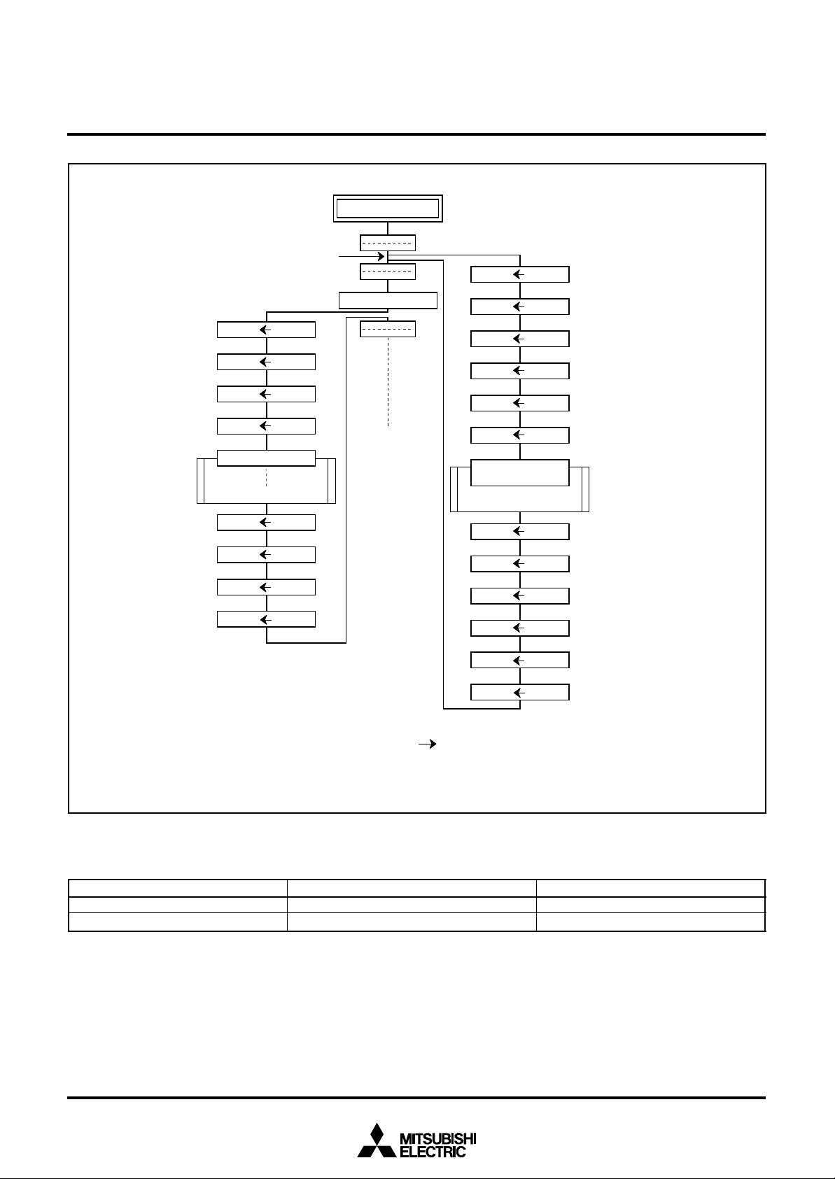
O n - g o i n g R o u t i n
MITSUBISHI MICROCOMPUTERS
38C2 Group
SINGLE-CHIP 8-BIT CMOS MICROCOMPUTER
P u s h r e t u r n a d d r e s s
o n s t a c k
P O P re t u r n
a d d r e s s f r o m s t a c k
I n t e r r u p t r e q u e s t
M ( S )( P CH)
S ) –
( S )
M ( S )( P CL)
S ) –
( S )
S u b r o u t i n e
E x e c u t e R T S
S ) +
( S )
( P CL)M ( S )
S ) +
( S )
( P CH)M ( S )
( N o t e )
(
(
1
(
(
M ( S )( P CH)
E x e c u t e J S R
1
1
1
S ) –
( S )
(
M ( S )( P CL)
S ) –
( S )
(
M ( S )( P S )
S ) –
( S )
(
I n t e r r u p t
S e r v i c e R o u t i n e
E x e c u t e R T I
S ) +
( S )
(
( P S )M ( S )
S ) +
( S )
(
( P CL)M ( S )
S ) +
( S )
(
1
P u s h r e t u r n a d d r e s s
o n s t a c k
1
P u s h c o n t e n t s o f p r o c e s s o r
s t a t u s r e g i s t e r o n s t a c k
1
I F l a g i s s e t f r o m “ 0 ” t o “ 1 ”
F e t c h t h e j u m p v e c t o r
1
P O P c o n t e n t s o f
p r o c e s s o r s t a t u s
r e g i s t e r f r o m s t a c k
1
P O P r e t u r n
a d d r e s s
1
f r o m s t a c k
N o t e: C o n d i t i o n f o r a c c e p t a n c e o f a n i n t e r r u p t I n t e r r u p t e n a b l e f l a g i s “ 1 ”
Fig. 6 Register push and pop at interrupt generation and subroutine call
Table 4 Push and pop instructions of accumulator or processor status register
Push instruction to stack
Accumulator
Processor status register
I n t e r r u p t d i s a b l e f l a g i s “ 0 ”
PHA
PHP
( P CH)M ( S )
Pop instruction from stack
PLA
PLP
8
Page 9
PRELIMINARY
Notice: This is not a final specification.
Some parametric limits are subject to change.
MITSUBISHI MICROCOMPUTERS
38C2 Group
SINGLE-CHIP 8-BIT CMOS MICROCOMPUTER
[Processor Status Register (PS)]
The processor status register is an 8-bit register consisting of 5 flags
which indicate the status of the processor after an arithmetic operation and 3 flags which decide MCU operation. Branch operations
can be performed by testing the Carry (C) flag , Zero (Z) flag, Overflow (V) flag, or the Negative (N) flag. In decimal mode, the Z, V, N
flags are not valid.
• Bit 0: Carry flag (C)
The C flag contains a carry or borrow generated by the arithmetic
logic unit (ALU) immediately after an arithmetic operation. It can
also be changed by a shift or rotate instruction.
• Bit 1: Zero flag (Z)
The Z flag is set if the result of an immediate arithmetic operation
or a data transfer is “0”, and cleared if the result is anything other
than “0”.
• Bit 2: Interrupt disable flag (I)
The I flag disables all interrupts except for the interrupt generated
by the BRK instruction.
Interrupts are disabled when the I flag is “1”.
• Bit 3: Decimal mode flag (D)
The D flag determines whether additions and subtractions are executed in binary or decimal. Binary arithmetic is executed when
this flag is “0”; decimal arithmetic is executed when it is “1”.
Decimal correction is automatic in decimal mode. Only the ADC
and SBC instructions can be used for decimal arithmetic.
• Bit 4: Break flag (B)
The B flag is used to indicate that the current interrupt was generated by the BRK instruction. The BRK flag in the processor status
register is always “0”. When the BRK instruction is used to generate an interrupt, the processor status register is pushed onto the
stack with the break flag set to “1”.
• Bit 5: Index X mode flag (T)
When the T flag is “0”, arithmetic operations are performed between accumulator and memory. When the T flag is “1”, direct arith-
metic operations and direct data transfers are enabled between
memory locations.
• Bit 6: Overflow flag (V)
The V flag is used during the addition or subtraction of one byte of
signed data. It is set if the result exceeds +127 to -128. When the
BIT instruction is executed, bit 6 of the memory location operated
on by the BIT instruction is stored in the overflow flag.
• Bit 7: Negative flag (N)
The N flag is set if the result of an arithmetic operation or data
transfer is negative. When the BIT instruction is executed, bit 7 of
the memory location operated on by the BIT instruction is stored in
the negative flag.
Table 5 Set and clear instructions of each bit of processor status register
Set instruction
Clear instruction
C flag
SEC
CLC
Z flag
–
–
I flag
SEI
CLI
D flag
SED
CLD
B flag
–
–
T flag
SET
CLT
V flag
–
CLV
N flag
–
–
9
Page 10
PRELIMINARY
Notice: This is not a final specification.
Some parametric limits are subject to change.
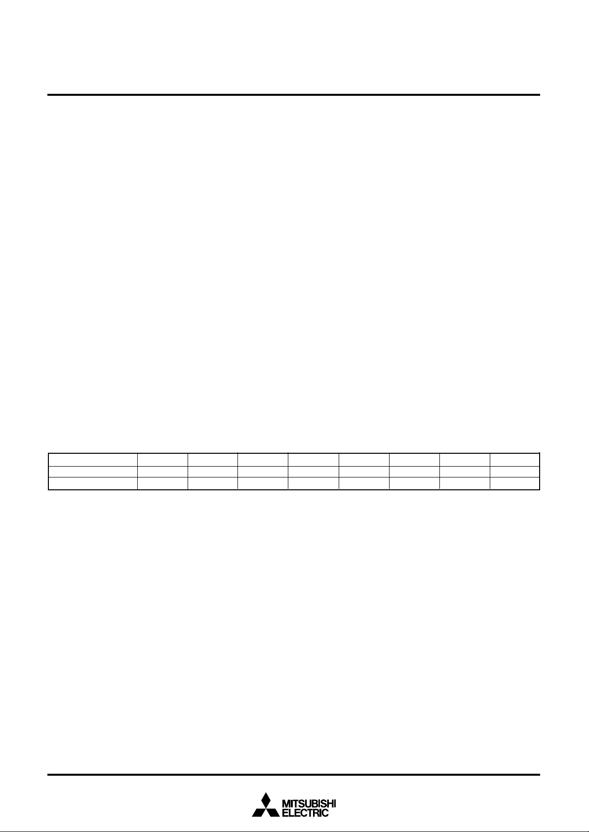
[CPU Mode Register (CPUM)] 003B16
The CPU mode register contains the stack page selection bit and
the control bit for the internal system clock.
The CPU mode register is allocated at address 003B16.
MITSUBISHI MICROCOMPUTERS
38C2 Group
SINGLE-CHIP 8-BIT CMOS MICROCOMPUTER
b7 b0
Fig. 7 Structure of CPU mode register
CPU mode register
(CPUM (CM) : address 003B
Processor mode bits
b1 b0
0 0 : Single-chip mode
0 1 :
1 0 :
1 1 :
Stack page selection bit
0 : RAM in the zero page is used as stack area
Not available
16
)
1 : RAM in page 1 is used as stack area
Not used (returns “1” when read)
(Do not write “0” to this bit.)
Main clock (X
b5 b4
0 0 : X
0 1 : X
1 0 : X
1 1 : X
System clock control bits
b7 b6
0 0 : X
0 1 : X
1 0 : X
1 1 : X
IN–XOUT
) d
ivision ratio selection bits
IN
/8 (frequency/8 mode)
IN
/4 (frequency/4 mode)
IN
/2 (frequency/2 mode)
IN
(through mode)
IN
stop, X
CIN
IN
oscillating, X
IN
oscillating, X
IN
oscillating, X
oscillating, system clock = X
CIN
CIN
CIN
stop, system clock = X
oscillating, system clock = X
oscillating, system clock = X
CIN
IN
CIN
IN
10
Page 11

PRELIMINARY
Notice: This is not a final specification.
Some parametric limits are subject to change.
MITSUBISHI MICROCOMPUTERS
38C2 Group
SINGLE-CHIP 8-BIT CMOS MICROCOMPUTER
MEMORY
Special Function Register (SFR) Area
The Special Function Register area in the zero page contains control
registers such as I/O ports and timers.
RAM
RAM is used for data storage and for stack area of subroutine calls
and interrupts.
ROM
The first 128 bytes and the last 2 bytes of ROM are reserved for
device testing and the rest is user area for storing programs.
Interrupt Vector Area
The interrupt vector area contains reset and interrupt vectors.
R A M a r e a
R A M s i z e
( b y t e s )
1 9 2
2 5 6
3 8 4
5 1 2
6 4 0
7 6 8
8 9 6
1 0 2 4
1 5 3 6
2 0 4 8
ROM area
R O M s i z e
( b y t e s )
4 0 9 6
8 1 9 2
1 2 2 8 8
1 6 3 8 4
2 0 4 8 0
2 4 5 7 6
2 8 6 7 2
3 2 7 6 8
3 6 8 6 4
4 0 9 6 0
4 5 0 5 6
4 9 1 5 2
5 3 2 4 8
5 7 3 4 4
6 1 4 4 0
A d d r e s s
X X X X
1 6
0 0 F F
1 6
0 1 3 F
1 6
0 1 B F
1 6
0 2 3 F
1 6
0 2 B F
1 6
0 3 3 F
1 6
0 3 B F
1 6
0 4 3 F
1 6
0 6 3 F
1 6
0 8 3 F
1 6
Address
YYYY
16
F 0 0 0
1 6
E 0 0 0
1 6
D 0 0 0
1 6
C 0 0 0
1 6
B 0 0 0
1 6
A 0 0 0
1 6
9 0 0 0
1 6
8 0 0 0
1 6
7 0 0 0
1 6
6 0 0 0
1 6
5 0 0 0
1 6
4 0 0 0
1 6
3 0 0 0
1 6
2 0 0 0
1 6
1 0 0 0
1 6
Address
ZZZZ
16
F 0 8 0
1 6
E 0 8 0
1 6
D 0 8 0
1 6
C 0 8 0
1 6
B 0 8 0
1 6
A 0 8 0
1 6
9 0 8 0
1 6
8 0 8 0
1 6
7 0 8 0
1 6
6 0 8 0
1 6
5 0 8 0
1 6
4 0 8 0
1 6
3 0 8 0
1 6
2 0 8 0
1 6
1 0 8 0
1 6
RAM
ROM
Zero Page
Access to this area with only 2 bytes is possible in the zero page
addressing mode.
Special Page
Access to this area with only 2 bytes is possible in the special page
addressing mode.
0 0 0 0
0 0 4 0
0 0 4 C
0100
XXXX
0 8 4 0
0 F E 0
1 0 00
Y Y Y Y
Z Z Z Z
F F 0 0
F F D C
F F F E
F F F F
1 6
1 6
16
16
1 6
1 6
1 6
1 6
1 6
1 6
1 6
1 6
1 6
1 6
S F R a r e a
L C D d i s p l a y R A M a r e a
R e s e r v e d a r e a
N o t u s e d
S F R a r e a
R e s e r v e d R O M a r e a
( 1 2 8 b y t e s )
Interrupt vector area
R e s e r v e d R O M a r e a
Zero
page
S p e c i a l
p a g e
Fig. 8 Memory map diagram
11
Page 12
PRELIMINARY
Notice: This is not a final specification.
Some parametric limits are subject to change.
MITSUBISHI MICROCOMPUTERS
38C2 Group
SINGLE-CHIP 8-BIT CMOS MICROCOMPUTER
Port P0 (P0)
0000
16
Port P0 direction register (P0D)
0001
16
Port P1 (P1)
0002
16
Port P1 direction register (P1D)
0003
16
Port P2 (P2)
0004
16
Port P2 direction register (P2D)
0005
16
Port P3 (P3)
0006
16
Port P3 direction register (P3D)
0007
16
Port P4 (P4)
0008
16
Port P4 direction register (P4D)
0009
16
Port P5 (P5)
000A
16
Port P5 direction register (P5D)
000B
16
Port P6 (P6)
000C
16
Port P6 direction register (P6D)
000D
16
000E
16
000F
16
0010
16
0011
16
0012
16
0013
16
0014
16
0015
16
0016
16
0017
16
Clock output control register (CKOUT)
0018
16
A-D control register (ADCON)
0019
16
A-D conversion register (low-order) (ADL)
001A
16
A-D conversion register (high-order) (ADH)
001B
16
Transmit/receive buffer register 1 (TB1/RB1)
001C
16
Serial I/O1 status register (SIO1STS)
001D
16
Transmit/receive buffer register 2 (TB2/RB2)
001E
16
Serial I/O2 status register (SIO2STS)
001F
16
0020
16
Timer 1 (T1)
Timer 2 (T2)
0021
16
Timer 3 (T3)
0022
16
Timer 4 (T4)
0023
16
0024
16
PWM01 register (PWM01)
0025
16
Timer 12 mode register (T12M)
0026
16
Timer 34 mode register (T34M)
0027
16
Compare register (low-order) (COMPL)
0028
16
0029
16
Compare register (high-order) (COMPH)
002A
16
Timer X (low-order) (TXL)
002B
16
Timer X (high-order) (TXH)
002C
16
Timer X (extension) (TXEX)
002D
16
Timer Y (low-order) (TYL)
002E
16
Timer Y (high-order) (TYH)
002F
16
Timer X mode register (TXM)
0030
16
Timer Y mode register (TYM)
0031
16
0032
16
0033
16
0034
16
0035
16
0036
16
Watchdog timer control register (WDTCON)
0037
16
LCD power control register (VLCON)
0038
16
LCD mode register (LM)
0039
16
Interrupt edge selection register (INTEDGE)
003A
16
003B
16
CPU mode register (CPUM)
Interrupt request register 1 (IREQ1)
003C
16
Interrupt request register 2 (IREQ2)
003D
16
003E
16
Interrupt control register 1 (ICON1)
Interrupt control register 2 (ICON2)
003F
16
Serial I/O1 control register (SIO1CON)
0FE0
16
UART1 control register (UART1CON)
0FE1
16
Baudrate generator 1 (BRG1)
0FE2
16
Serial I/O2 control register (SIO2CON)
0FE3
16
UART2 control register (UART2CON)
0FE4
16
Baudrate generator 2 (BRG2)
0FE5
16
0FE6
16
0FE7
16
0FE8
16
0FE9
16
0FEA
16
0FEB
16
0FEC
16
0FED
16
0FEE
16
0FEF
16
Fig. 9 Memory map of special function register (SFR)
12
0FF0
16
Oscillation output control register (OSCOUT)
0FF1
16
PULL register (PULL)
0FF2
16
Key input control register (KIC)
0FF3
16
Timer 1234 mode register (T1234M)
0FF4
16
Timer X control register (TXCON)
Timer 12 frequency division selection register (PRE12)
0FF5
16
Timer 34 frequency division selection register (PRE34)
0FF6
16
Timer XY frequency division selection register (PREXY)
0FF7
16
0FF8
16
Segment output disable register 0 (SEG0)
0FF9
16
Segment output disable register 1 (SEG1)
0FFA
16
Segment output disable register 2 (SEG2)
0FFB
16
Timer Y mode register 2 (TYM2)
0FFC
16
0FFD
16
0FFE
16
Flash memory control register (FMCR)
0FFF
16
Reserved area
Page 13
PRELIMINARY
Notice: This is not a final specification.
Some parametric limits are subject to change.
MITSUBISHI MICROCOMPUTERS
38C2 Group
SINGLE-CHIP 8-BIT CMOS MICROCOMPUTER
I/O PORTS
Direction Registers
The I/O ports P0–P6 have direction registers which determine the
input/output direction of each individual pin. Each bit in a direction
register corresponds to one pin, each pin can be set to be input port
or output port.
When “0” is written to the bit of the direction register , the corresponding pin becomes an input pin. As for ports P0–P2, when “1” is written
to the bit of the direction register and the segment output disable
register, the corresponding pin becomes an output pin. As for ports
P3–P6, when “1” is written to the bit of the direction register, the
corresponding pin becomes an output pin.
If data is read from a pin set to output, the value of the port output
latch is read, not the value of the pin itself. Pins set to input are floating. If a pin set to input is written to, only the port output latch is
written to and the pin remains floating.
Pull-up Control
Each individual bit of ports P0–P2 can be pulled up with a program
by setting direction registers and segment output disable registers 0
to 2 (addresses 0FF816 to 0FFA16).
The pin is pulled up by setting “0” to the direction register and “1” to
the segment output disable register.
By setting the PULL register (address 0FF116), ports P3–P6 can control pull-up with a program.
However, the contents of PULL register do not affect ports programmed as the output ports.
b7 b0
b7 b0
b7 b0
PULL register
(PULL : address 0FF1
P30–P33 pull-up
P3
4
–P37 pull-up
0
–P43 pull-up
P4
P4
4
–P47 pull-up
P5
0
–P53 pull-up
P5
4
–P57 pull-up
0
–P62 pull-up
P6
Not used (return “0” when read)
Segment output disable register 0
(SEG0 : address 0FF8
P00 pull-up
P0
1
pull-up
P0
2
pull-up
3
pull-up
P0
P0
4
pull-up
5
pull-up
P0
P0
6
pull-up
7
pull-up
P0
Segment output disable register 1
(SEG1 : address 0FF9
P10 pull-up
P1
1
pull-up
P1
2
pull-up
P1
3
pull-up
4
pull-up
P1
P1
5
pull-up
P1
6
pull-up
P1
7
pull-up
16
)
16
)
16
)
0: No pull-up
1: Pull-up
S e g m e n t o u t p u t
d i s a b l e r e g i s t e r
D i r e c t i o n r e g i s t e r
“ 0 ”
“ 1 ”
“ 0 ”“
I n p u t p o r t
N o p u l l - u p
S e g m e n t
o u t p u t
I n p u t p o r t
P u l l - u p
P o r t o u t p u t
Fig. 10 Structure of ports P0 to P2
b7 b0
1
”
I n i t i a l s t a t e
Note: The PULL register and segment output disable register
affect only ports programmed as the input ports.
Segment output disable register 2
(SEG2 : address 0FFA
P2
0
pull-up
P2
1
pull-up
P2
2
pull-up
P2
3
pull-up
4
pull-up
P2
P2
5
pull-up
P2
6
pull-up
P2
7
pull-up
16
)
0: No pull-up
1: Pull-up
Fig. 11 Structure of PULL register and segment output disable register
13
Page 14
MITSUBISHI MICROCOMPUTERS
PRELIMINARY
Notice: This is not a final specification.
Some parametric limits are subject to change.
Table 6 List of I/O port function
Pin
P00/SEG0 –
P03/SEG3
P04/SEG4 –
P07/SEG7
P10/SEG8 –
P17/SEG15
P20/SEG16 –
P25/SEG21
P26/SEG22/VL1
P27/SEG23/VL2
P30/SRDY2
P31/SCLK2
P32/TxD2
P33/RxD2
P34/INT2
P35/TXOUT
P36/T2OUT/φ
P37/CNTR0
P40/OOUT0/AN0
P41/OOUT1/AN1
P42/AN2–
P45/AN5
P46/RTP0/AN6
P47/RTP1/AN7
P50/INT0
P51/INT1
P52/T3OUT/PWM0
P53/T4OUT/PWM1
P54/RxD1
P55/TxD1
P56/SCLK1
P57/SRDY1
P60/CNTR1
P61/XCIN
P62/XCOUT
COM0–COM3
Notes 1: For details of how to use double/triple function ports as function I/O ports, refer to the applicable sections.
2: Make sure that the input level at each pin is either 0 V or V
When an input level is at an intermediate potential, a current will flow from V
Name
Port P0
Port P1
Port P2
Port P3
Port P4
Port P5
Port P6
Common
Input/Output
Input/Output,
individual bits
Input/Output,
individual bits
Input/Output,
individual bits
Input/Output,
individual bits
Input/Output,
individual bits
Input/Output,
individual bits
Input/Output,
individual bits
Output
I/O format
CMOS compatible
input level
CMOS 3-state output
CMOS compatible
input level
CMOS 3-state output
CMOS compatible
input level
CMOS 3-state output
CMOS compatible
input level
CMOS 3-state output
CMOS compatible
input level
CMOS 3-state output
CMOS compatible
input level
CMOS 3-state output
CMOS compatible
input level
CMOS 3-state output
LCD common output
CC during execution of the STP instruction.
LCD segment
output
Serial I/O2 function I/O
External interrupt input
Timer X output
Timer 2 output
Timer X function input
A-D conversion
input
External interrupt input
Timer 3 output
Timer 4 output
PWM output
Serial I/O1
function I/O
Timer Y function input
Sub-clock oscillation circuit
CC to VSS through the input-stage gate.
SINGLE-CHIP 8-BIT CMOS MICROCOMPUTER
Non-port function
Key input
(key-on wakeup)
interrupt input
LCD power
input
Oscillation
external
output
Real time
port function
output
Key input
(key-on wakeup)
interrupt input
38C2 Group
Related SFRs
Segment output disable
register 1
Segment output disable
register 2
Segment output disable
register 3
PULL register
Serial I/O2 control register
Serial I/O2 status register
UART2 control register
PULL register
Interrupt edge selection
register
PULL register
Timer X mode register
Timer 12 mode register
PULL register
Timer X mode register
PULL register
A-D control register
PULL register
A-D control register
Timer Y mode register
PULL register
Interrupt edge selection
register
PULL register
Timer 12 mode register
PULL register
Serial I/O1 control register
Serial I/O1 status register
UART1 control register
PULL register
Timer Y mode register
PULL register
CPU mode register
LCD mode register
Ref. No.
(1)
(2)
(3)
(4)
(5)
(6)
(7)
(8)
(9)
(7)
(11)
(10)
(11)
(7)
(9)
(12)
(13)
(14)
(15)
(7)
(16)
(17)
(18)
14
Page 15
PRELIMINARY
t
t
Notice: This is not a final specification.
Some parametric limits are subject to change.
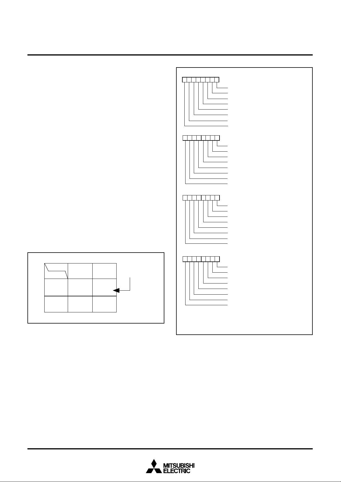
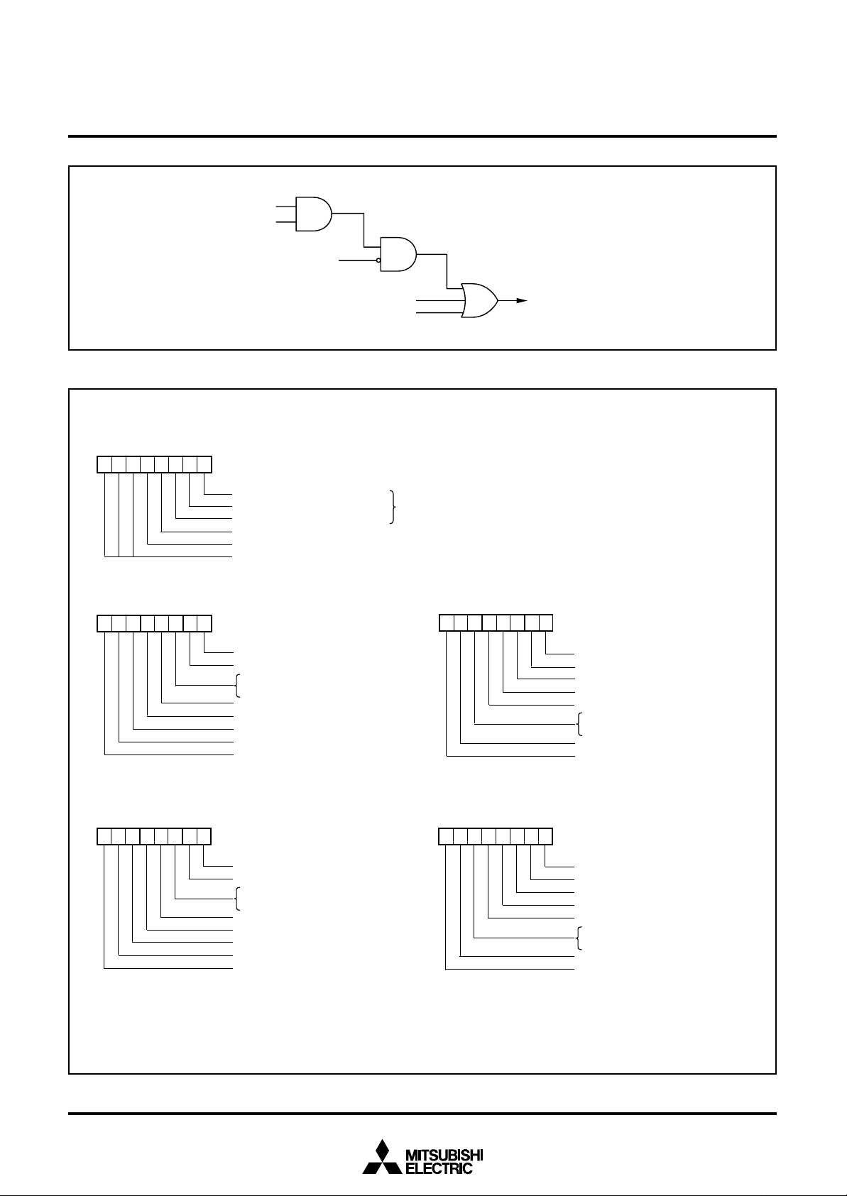
( 1 ) P o r t s P 00– P 0
S e g m e n t o u t p u t d i s a b l e b i t
3
V
MITSUBISHI MICROCOMPUTERS
38C2 Group
SINGLE-CHIP 8-BIT CMOS MICROCOMPUTER
( 2 ) P o r t s P 04– P 07, P 1 , P 2
V
L 2
/ V
L 2
/ V
L 3
S e g m e n t o u t p u t d i s a b l e b i t
L 3
S e g m e n t d a t a
S e g m e n t o u t p u t d i s a b l e b i t
D i r e c t i o n r e g i s t e r
D a t a b u s
K e y - o n w a k e u p
i n t e r r u p t i n p u t
(3) Port P3
Serial I/O mode selection bit
0
Serial I/O enable bit
RDY
output enable b it
S
D i r e c t i o n r e g i s t e r
P o r t l a t c h
V
L 1
/ V
S S
K e y i n p u t c o n t r o l
P u l l - u p c o n t r o l
S e g m e n t d a t a
Segment output disable bit
D i r e c t i o n r e g i s t e r
D a t a b u s
( 4 ) P o r t P 3
Serial I/O synchronous
1
clock selection bit
Serial I/O enable bit
Serial I/O mode selection bi
Serial I/O enable bi
Direction register
P o r t l a t c h
V
L 1
/ V
S S
L C D p o w e r i n p u t ( V
o n l y f o r P 26, P 2
L 1
, V
L 2
)
7
P u l l - u p c o n t r o l
Data bus
Serial I/O ready output
(5) Port P3
Data bus
P o r t l a t c h
2
P 3
2
/ T x D2 P - c h a n n e l
S e r i a l I / O e n a b l e b i t
o u t p u t d i s a b l e b i t
T r a n s m i t e n a b l e b i t
D i r e c t i o n r e g i s t e r
P o r t l a t c h
Serial I/O output
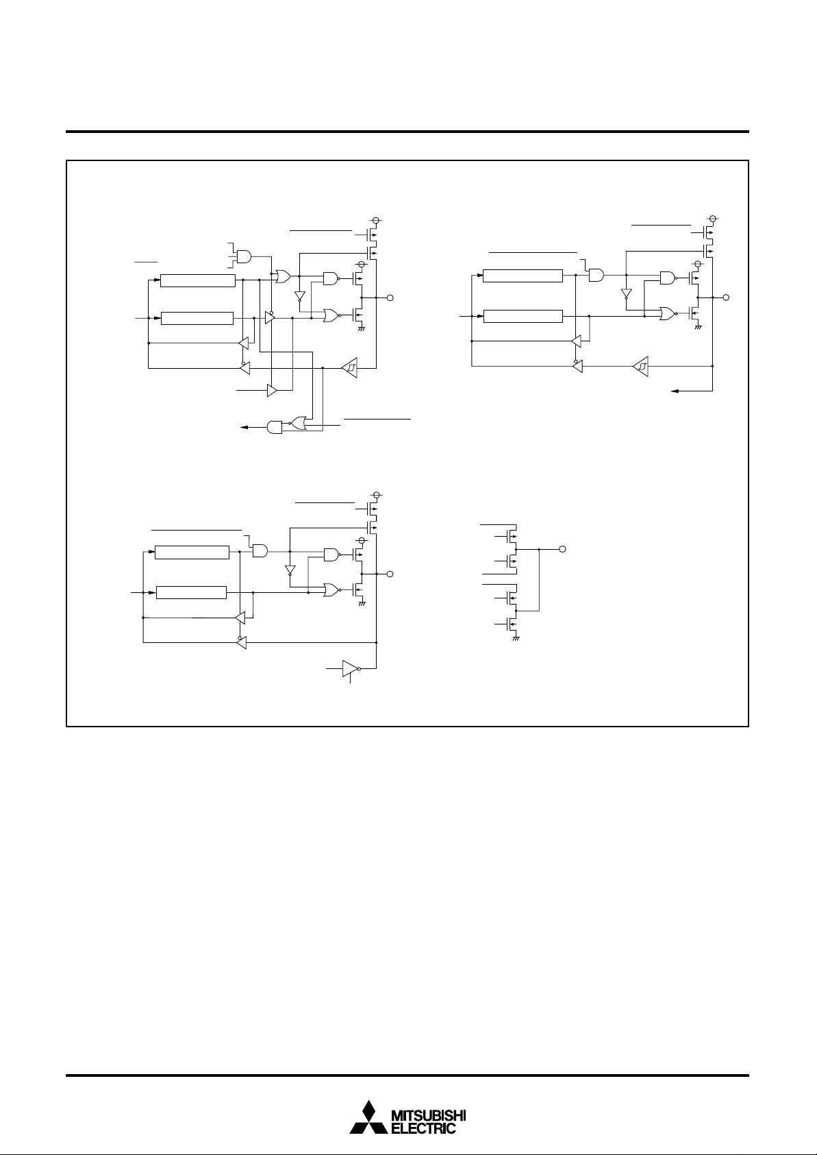
Fig. 12 Port block diagram (1)
P u l l - u p c o n t r o l
Data bus
(6) Port P3
Data bus
Port latch
S e r i a l I / O c l o c k o u t p u t
3
S e r i a l I / O e n a b l e b i t
R e c e i v e e n a b l e b i t
Direction register
P o r t l a t c h
S e r i a l I / O c l o c k i n p u t
P u l l - u p c o n t r o l
S e r i a l I / O i n p u t
15
Page 16
PRELIMINARY
t
t
Notice: This is not a final specification.
Some parametric limits are subject to change.
MITSUBISHI MICROCOMPUTERS
38C2 Group
SINGLE-CHIP 8-BIT CMOS MICROCOMPUTER
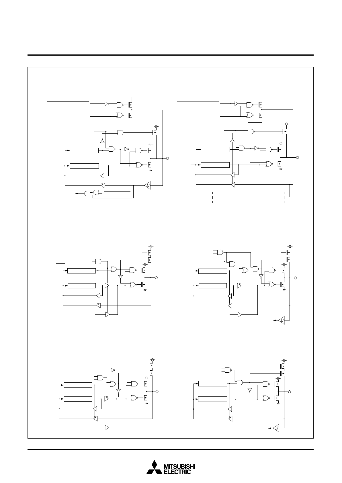
( 7 ) P o r t s P 34, P 37, P 50, P 51, P 6
Direction register
Data bus
C N T R0, C N T R1 i n t e r r u p t i n p u t
( 9 ) P o r t s P 36, P 52, P 5
D a t a b u s
T i m e r o u t p u t / S y s t e m c l o c k φ o u t p u t
( 1 1 ) P o r t s P 40, P 41, P 46, P 4
Port latch
0
– I N T2 i n t e r r u p t i n p u t
I N T
3
D i r e c t i o n r e g i s t e r
P o r t l a t c h
P o r t / T i m e r o u t p u t s e l e c t i o n
T i m e r o u t p u t / P W M o u t p u t
7
Direction register
0
P u l l - u p c o n t r o l
Pull-up control
P u l l - u p c o n t r o l
(8) Port P3
Data bus
5
D i r e c t i o n r e g i s t e r
P u l s e o u t p u t m o d e
T i m e r X o u t p u t
(10) Ports P42–P4
D a t a b u s
(12) Port P5
4
Serial I/O enable bi
Receive enable bi
Direction register
Pull-up control
Port latch
5
Pull-up control
D i r e c t i o n r e g i s t e r
P o r t l a t c h
A-D conversion input
A n a l o g i n p u t p i n s e l e c t i o n b i t
Pull-up control
Data bus
O s c i l l a t i o n o u t p u t c o n t r o l b i t /
( 1 3 ) P o r t P 5
D a t a b u s
K e y - o n w a k e u p i n t e r r u p t i n p u t
P o r t l a t c h
R e a l t i m e c o n t r o l b i t
O s c i l l a t i o n o u t p u t /
D a t a f o r r e a l t i m e p o r t
5
5
/ T x D1 P - c h a n n e l
P 5
S e r i a l I / O e n a b l e b i t
o u t p u t d i s a b l e b i t
T r a n s m i t e n a b l e b i t
Direction register
Port latch
S e r i a l I / O o u t p u t
Fig. 13 Port block diagram (2)
A - D c o n v e r s i o n i n p u t
Analog input pin selection bit
Pull-up control
K e y i n p u t c o n t r o l
D a t a b u s
Key-on wakeup interrupt input
(14) Port P5
S e r i a l I / O s y n c h r o n o u s c l o c k
S e r i a l I / O e n a b l e b i t
S e r i a l I / O m o d e s e l e c t i o n b i t
Data bus
6
s e l e c t i o n b i t
S e r i a l I / O e n a b l e b i t
Direction register
Port latch
Serial I/O clock output
K e y - o n w a k e u p i n t e r r u p t i n p u t
Port latch
Serial I/O input
K e y i n p u t c o n t r o l
Pull-up control
Serial I/O clock input
K e y i n p u t c o n t r o l
16
Page 17
PRELIMINARY
Notice: This is not a final specification.
Some parametric limits are subject to change.
MITSUBISHI MICROCOMPUTERS
38C2 Group
SINGLE-CHIP 8-BIT CMOS MICROCOMPUTER
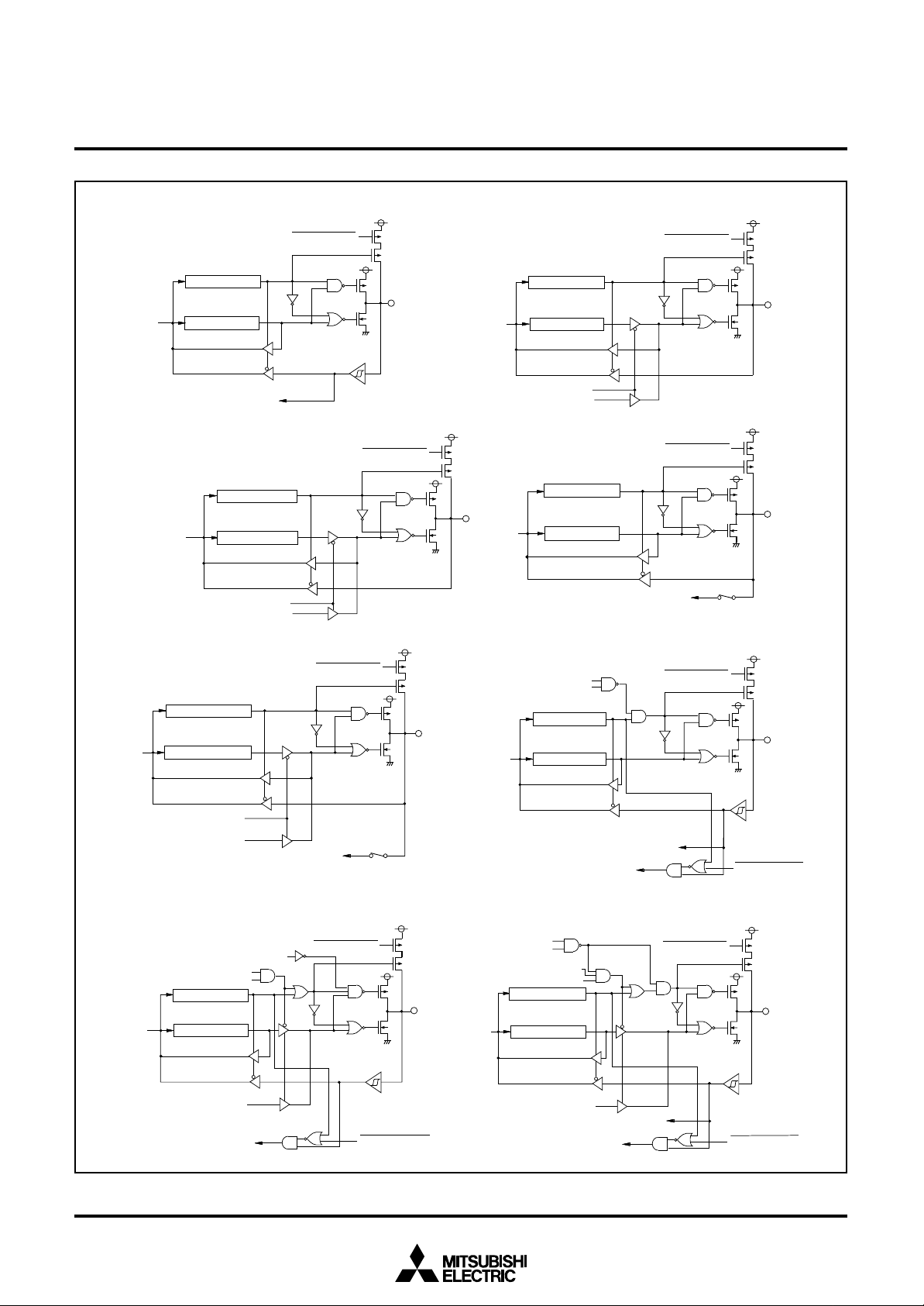
( 1 5 ) P o r t P 5
S e r i a l I / O m o d e s e l e c t i o n b i t
Data bus
K e y - o n w a k e u p i n t e r r u p t i n p u t
(17) Port P6
D a t a b u s
7
S e r i a l I / O e n a b l e b i t
R D Y
o u t p u t e n a b l e b i t
S
S e r i a l I / O r e a d y o u t p u t
2
X c o s c i l l a t i o n e n a b l e d
D i r e c t i o n r e g i s t e r
D i r e c t i o n r e g i s t e r
P o r t l a t c h
X c o s c i l l a t i o n e n a b l e d + P u l l - u p c o n t r o l
P o r t l a t c h
P u l l - u p c o n t r o l
Key input control
( 1 6 ) P o r t P 6
Data bus Port latch
( 1 7 ) C O M0– C O M
1
X c o s c i l l a t i o n e n a b l e d
Direction register
3
V
L3
V
L2
V
L1
Xc oscillation enabled + Pull-up control
Sub-clock generation circuit input
Gate input signal of
each gate depends
on the duty ratio
and bias values.
Fig. 14 Port block diagram (3)
Port P6
Oscillator
1
Xc oscillation enabled
V
SS
17
Page 18
PRELIMINARY
Notice: This is not a final specification.
Some parametric limits are subject to change.
MITSUBISHI MICROCOMPUTERS
38C2 Group
SINGLE-CHIP 8-BIT CMOS MICROCOMPUTER
INTERRUPTS
Interrupts occur by nineteen sources: six external, twelve internal,
and one software.
Interrupt Control
Each interrupt except the BRK instruction interrupt have both an interrupt request bit and an interrupt enable bit, and is controlled by the
interrupt disable flag. An interrupt occurs if the corresponding interrupt request and enable bits are “1” and the interrupt disable flag is
“0”.
Interrupt enable bits can be set or cleared by software. Interrupt request bits can be cleared by software, but cannot be set by software.
The BRK instruction interrupt and reset cannot be disabled with any
flag or bit. The I flag disables all interrupts except the BRK instruction
interrupt and reset. If several interrupts requests occurs at the same
time the interrupt with highest priority is accepted first.
Table 7 Interrupt vector addresses and priority
Interrupt Source
Reset (Note 2)
INT0
INT1
INT2
Key input
(key-on wakeup)
Serial I/O1 receive
Serial I/O1 transmit
Serial I/O2 receive
Serial I/O2 transmit
Timer X
Timer 1
Timer 2
Timer 3
Timer 4
CNTR0
Timer Y
CNTR1
A-D conversion
BRK instruction
Notes 1: Vector addresses contain interrupt jump destination addresses.
2: Reset function in the same way as an interrupt with the highest priority.
Priority
Vector Addresses (Note 1)
High
1
FFFD16
2
FFFB16
3
FFF916
4
FFF716
5
FFF516
6
FFF316
7
FFF116
8
FFEF16
9
FFED16
10
11
12
13
14
15
16
17
FFEB16
FFE916
FFE716
FFE516
FFE316
FFE116
FFDF16
FFDD16
Low
FFFC16
FFFA16
FFF816
FFF616
FFF416
FFF216
FFF016
FFEE16
FFEC16
FFEA16
FFE816
FFE616
FFE416
FFE216
FFE016
FFDE16
FFDC16
At reset
At detection of either rising or falling
edge of INT0 input
At detection of either rising or falling
edge of INT1 input
At detection of either rising or falling
edge of INT2 input
At falling of ports P00–P03, P54–P57
input logical level AND
At completion of serial I/O1 data receive
At completion of serial I/O1 transmit
shift or transmit buffer is empty
At completion of serial I/O2 data receive
At completion of serial I/O2 transmit
shift or transmit buffer is empty
At timer X underflow
At timer 1 underflow
At timer 2 underflow
At timer 3 underflow
At timer 4 underflow
At detection of either rising or falling
edge of CNTR0 input
At timer Y underflow
At detection of either rising or falling
edge of CNTR1 input
At completion of A-D conversion
At BRK instruction execution
Interrupt Operation
By acceptance of an interrupt, the following operations are automatically performed:
1.The processing being executed is stopped.
2.The contents of the program counter and processor status register are automatically pushed onto the stack.
3.The interrupt disable flag is set and the corresponding interrupt
request bit is cleared.
4.The interrupt jump destination address is read from the vector
table into the program counter.
■ Notes on Interrupts
When the active edge of an external interrupt (INT0 – INT2, CNTR0
or CNTR1) is set or an interrupt source where several interrupt source
is assigned to the same vector address is switched, the corresponding interrupt request bit may also be set. Therefore, take following
sequence:
(1) Disable the interrupt.
(2) Set the interrupt edge selection register (Timer X control reg-
ister for CNTR0, Timer Y mode register for CNTR1).
(3) Clear the set interrupt request bit to “0.”
(4) Enable the interrupt.
Interrupt Request
Generating Conditions
Non-maskable
External interrupt (active edge selectable)
External interrupt (active edge selectable)
Valid when INT2 interrupt is selected
External interrupt (active edge selectable)
Valid when key input interrupt is selected
External interrupt (falling valid)
Valid only when serial I/O1 is selected
Valid only when serial I/O1 is selected
Valid only when serial I/O2 is selected
Valid only when serial I/O2 is selected
Valid only when timer 1 interrupt is selected
Valid only when timer 2 interrupt is selected
External interrupt (active edge selectable)
External interrupt (active edge selectable)
Valid when A-D conversion interrupt is selected
Non-maskable software interrupt
Remarks
18
Page 19
PRELIMINARY
Notice: This is not a final specification.
Some parametric limits are subject to change.
Interrupt request bit
Interrupt enable bit
Interrupt disable flag (I)
MITSUBISHI MICROCOMPUTERS
38C2 Group
SINGLE-CHIP 8-BIT CMOS MICROCOMPUTER
Fig. 15 Interrupt control
b7 b0
b7 b0
BRK instruction
Interrupt edge selection register
16
(INTEDGE : address 003A
)
INT0 interrupt edge selection bit
1
interrupt edge selection bit
INT
INT
2
interrupt edge selection bit
2
/Key input interrupt switch bit
INT
Timer Y/CNTR
1
interrupt switch bit
Not used (return “0” when read)
(Do not write to “1”)
Interrupt request register 1
16
(IREQ1 : address 003C
)
INT0 interrupt request bit
1
interrupt request bit
INT
INT
2
interrupt request bit
Key input interrupt request bit
Serial I/O1 receive interrupt request bit
Serial I/O1 transmit interrupt request bit
Serial I/O2 receive interrupt request bit
Serial I/O2 transmit interrupt request bit
Timer X interrupt request bit
Reset
0 : Falling edge active
1 : Rising edge active
0 : INT2 interrupt
1 : Key input interrupt
0 : Timer Y interrupt
1 : CNTR
1
interrupt
b7 b0
Interrupt request
Interrupt request register 2
(IREQ2 : address 003D
Timer 1 interrupt request bit
Timer 2 interrupt request bit
Timer 3 interrupt request bit
Timer 4 interrupt request bit
CNTR
Timer Y interrupt request bit
CNTR
AD conversion interrupt request bit
Not used (returns “0” when read)
0 : No interrupt request issued
1 : Interrupt request issued
16
)
0
interrupt request bit
1
interrupt request bit
b7 b0
Interrupt control register 1
(ICON1 : address 003E
INT0 interrupt enable bit
1
interrupt enable bit
INT
INT
2
interrupt enable bit
Key input interrupt enable bit
Serial I/O1 receive interrupt enable bit
Serial I/O1 transmit interrupt enable bit
Serial I/O2 receive interrupt enable bit
Serial I/O2 transmit interrupt enable bit
Timer X interrupt enable bit
Fig. 16 Structure of interrupt-related registers
b7 b0
16
)
Interrupt control register 2
(ICON2 : address 003F
16
)
Timer 1 interrupt enable bit
Timer 2 interrupt enable bit
Timer 3 interrupt enable bit
Timer 4 interrupt enable bit
CNTR
0
interrupt enable bit
Timer Y interrupt enable bit
CNTR
1
interrupt enable bit
AD conversion interrupt enable bit
Not used (returns “0” when read)
(Do not write to “1”.)
0 : Interrupts disabled
1 : Interrupts enabled
19
Page 20

PRELIMINARY
Notice: This is not a final specification.
Some parametric limits are subject to change.
MITSUBISHI MICROCOMPUTERS
38C2 Group
SINGLE-CHIP 8-BIT CMOS MICROCOMPUTER
Key Input Interrupt (Key-on Wake-Up)
A key input interrupt request is generated by detecting the falling
edge from any pin of ports P0
input mode. In other words, it is generated when AND of input level
0–P03, P54–P57 that have been set to
P o r t P X x
“ L ” l e v e l o u t p u t
Segment output
disable register 1
Bit 3 = “1”
✽
3
o u t p u t
P 0
S e g m e n t o u t p u t
d i s a b l e r e g i s t e r 1
B i t 2 = “ 1 ”
✽
2
o u t p u t
P 0
Segment output
disable register 1
Bit 1 = “1”
✽
1
o u t p u t
P 0
Segment output
disable register 1
Bit 0 = “1”
✽
0
o u t p u t
P 0
✽
P 5
7
i n p u t
Port P0
direction register = “1”
✽✽
✽✽
✽✽
✽✽
P o r t P 5
d i r e c t i o n r e g i s t e r = “ 0 ”
✽✽
3
P o r t P 0
l a t c h
P o r t P 0
d i r e c t i o n r e g i s t e r = “ 1 ”
2
Port P0
latch
Port P0
direction register = “1”
1
Port P0
latch
Port P0
direction register = “1”
0
P o r t P 0
l a t c h
7
Port P5
7
latch
goes from “1” to “0”. An example of using a key input interrupt is
shown in Figure 17, where an interrupt request is generated by pressing one of the keys consisted as an active-low key matrix which inputs to ports P5
3
Key input control
register = “1”
2
Key input control
register = “1”
1
Key input control
register = “1”
0
Key input control
register = “1”
Key input control
register = “1”
4–P57.
K e y i n p u t i n t e r r u p t r e q u e s t
P o r t P 0
I n p u t r e a d i n g c i r c u i t
Port P5
6
P 5
P5
P 5
6
input
5
i n p u t
4
i n p u t
✽
✽
✽
PULL register
Bit 5 = “1”
direction register = “0”
✽✽
Port P5
latch
P o r t P 5
5
d i r e c t i o n r e g i s t e r = “ 0 ”
✽✽
Port P5
latch
Port P5
4
direction register = “0”
✽✽
Port P5
latch
K e y i n p u t c o n t r o l
r e g i s t e r = “ 1 ”
6
K e y i n p u t c o n t r o l
r e g i s t e r = “ 1 ”
5
Key input control
register = “1”
4
✽ P-channel transistor for pull-up
✽ ✽ CMOS output buffer
Fig. 17 Connection example when using key input interrupt and ports P0 and P5 block diagram
20
P o r t P 5
I n p u t r e a d i n g c i r c u i t
Page 21

PRELIMINARY
Notice: This is not a final specification.
Some parametric limits are subject to change.
A key input interrupt is controlled by the key input control register and
port direction registers. When the key input interrupt is enabled, set
“1” to the key input control register. A key input of any pin of ports
P00–P03, P54–P57 that have been set to input mode is accepted.
MITSUBISHI MICROCOMPUTERS
38C2 Group
SINGLE-CHIP 8-BIT CMOS MICROCOMPUTER
b7 b0
Key input control register
(KIC : address 0FF2
P54 key input control bit
5
key input control bit
P5
P5
6
key input control bit
7
key input control bit
P5
P0
0
key input control bit
1
key input control bit
P0
P0
2
key input control bit
3
key input control bit
P0
0 : Key input interrupt disabled
1 : Key input interrupt enabled
Fig. 18 Structure of key input control register
16
)
21
Page 22

PRELIMINARY
Notice: This is not a final specification.
Some parametric limits are subject to change.
TIMERS
8-Bit Timer
The 38C2 group has four built-in timers : Timer 1, Timer 2, Timer 3,
and Timer 4.
Each timer has the 8-bit timer latch. All timers are down-counters.
When the timer reaches “00
reloaded into the timer with the next count pulse. In this mode, the
interrupt request bit corresponding to that timer is set to “1.”
The count can be stopped by setting the stop bit of each timer to “1.”
● Frequency Divider For Timer
Timer 1, timer 2, timer 3 and timer 4 have the frequency divider for
the count source. The count source of the frequency divider is switched
to XIN or XCIN by the CPU mode register. The frequency divider is
controlled by the 3-bit register. The division ratio can be selected
from as follows;
1/1, 1/2, 1/16, 1/32, 1/64, 1/128, 1/256, 1/1024 of f(XIN) or f(XCIN).
16,” the contents of the timer latch is
MITSUBISHI MICROCOMPUTERS
38C2 Group
SINGLE-CHIP 8-BIT CMOS MICROCOMPUTER
●Timer 1, Timer 2
The count sources of timer 1 and timer 2 can be selected by setting
the timer 12 mode register.
When f(XCIN) is selected as the count source, counting can be performed regardless of XCIN oscillation. However, when XCIN is stopped,
the external pulse input from XCIN pin is counted. Also, by the timer
12 mode register, each time timer 2 underflows, the signal of which
polarity is inverted can be output from P36/T2OUT pin.
At reset, all bits of the timer 12 mode register are cleared to “0,” timer
1 is set to “FF16,” and timer 2 is set to “0116.”
When executing the STP instruction, previously set the wait time at
return.
● Timer 3, Timer 4
The count sources of timer 3 and timer 4 can be selected by setting
the timer 34 mode register. Also, by the timer 34 mode register, each
time timer 3 or timer 4 underflows, the signal of which polarity is
inverted can be output from P52/T3OUT pin or P53/T4OUT pin.
● Timer 3 PWM0 Mode, Timer 4 PWM1 Mode
A PWM rectangular waveform corresponding to the 10-bit accuracy
can be output from the P52/PWM0 pin and P53/PWM1 pin by setting the timer 34 mode register and PWM01 register (refer to Figure
21).
The “n” is the value set in the timer 3 (address 002216) or the timer
4 (address 002316). The “ts” is one period of timer 3 or timer 4
count source.
One output pulse is the short interval. Four output pulses are the
long interval. “H” width of the short interval is obtained by n ✕ ts.
However, in the long interval, “H” width of output pulse is extended
for ts which is set by the PWM01 register (address 002416).
22
Page 23

PRELIMINARY
Notice: This is not a final specification.
Some parametric limits are subject to change.
MITSUBISHI MICROCOMPUTERS
38C2 Group
SINGLE-CHIP 8-BIT CMOS MICROCOMPUTER
b7
b7
b7
b0
Timer 12 mode register
(T12M: address 0025
Timer 1 count stop bit
0 : Count operation
1 : Count stop
Timer 2 count stop bit
0 : Count operation
1 : Count stop
Timer 1 count source selection bits
b3 b2
0 0 : Frequency divider for Timer 1
0 1 : f(X
1 0 : Underflow of Timer Y
1 1 : Not available
Timer 2 count source selection bits
b5 b4
0 0 : Underflow of Timer 1
0 1 : f(X
1 0 : Frequency divider for Timer 2
1 1 : Not available
Timer 2 output selection bit (P3
0 : I/O port
1 : Timer 2 output
2OUT
output edge switch bit
T
0 : Start at “L” output
1 : Start at “H” output
b0
Timer 34 mode register
(T34M: address 0026
Timer 3 count stop bit
0 : Count operation
1 : Count stop
Timer 4 count stop bit
0 : Count operation
1 : Count stop
Timer 3 count source selection bit
0 : Frequency divider for Timer 3
1 : Underflow of Timer 2
Timer 4 count source selection bits
b4 b3
0 0 : Frequency divider for Timer 4
0 1 : Underflow of Timer 3
1 0 : Underflow of Timer 2
1 1 : Not available
Timer 3 operating mode selection bit
0 : Timer mode
1 : PWM mode
Timer 4 operating mode selection bit
0 : Timer mode
1 : PWM mode
Not used (returns “0” when read)
b0
Timer 1234 mode register
(T1234M: address 0FF3
3OUT
output edge switch bit
T
0 : Start at “L” output
1 : Start at “H” output
4OUT
output edge switch bit
T
0 : Start at “L” output
1 : Start at “H” output
Timer 3 output selection bit (P5
0 : I/O port
1 : Timer 3 output
Timer 4 output selection bit (P5
0 : I/O port
1 : Timer 4 output
Timer 2 write control bit
0 : Write data to both timer latch and timer
1 : Write data to timer latch only
Timer 3 write control bit
0 : Write data to both timer latch and timer
1 : Write data to timer latch only
Timer 4 write control bit
0 : Write data to both timer latch and timer
1 : Write data to timer latch only
Not used (returns “0” when read)
16
)
CIN
)
CIN
)
16
)
16
)
6
)
2
)
3
)
b7
b7
b0
PWM01 register
(PWM01: address 0024
PWM0 set bits
b1 b0
0 0 : No extended
0 1 : Extended once in four periods
1 0 : Extended twice in four periods
1 1 : Extended three times in four periods
PWM1 set bits
b3 b2
0 0 : No extended
0 1 : Extended once in four periods
1 0 : Extended twice in four periods
1 1 : Extended three times in four periods
Not used (returns “0” when read)
b0
Timer 12 frequency division selection register
(PRE12: address 0FF5
Timer 1 frequency division selection bits
b2 b1 b0
0 0 0 : 1/16 ✕ f(X
0 0 1 : 1/1 ✕ f(X
0 1 0 : 1/2 ✕ f(X
0 1 1 : 1/32 ✕ f(X
1 0 0 : 1/64 ✕ f(X
1 0 1 : 1/128 ✕ f(X
1 1 0 : 1/256 ✕ f(X
1 1 1 : 1/1024 ✕ f(X
Timer 2 frequency division selection bits
b5 b4 b3
0 0 0 : 1/16 ✕ f(X
0 0 1 : 1/1 ✕ f(X
0 1 0 : 1/2 ✕ f(X
0 1 1 : 1/32 ✕ f(X
1 0 0 : 1/64 ✕ f(X
1 0 1 : 1/128 ✕ f(X
1 1 0 : 1/256 ✕ f(X
1 1 1 : 1/1024 ✕ f(X
16
)
16
)
IN
) or 1/16 ✕ f(X
IN
) or 1/1 ✕ f(X
IN
) or 1/2 ✕ f(X
IN
) or 1/32 ✕ f(X
IN
) or 1/64 ✕ f(X
IN
) or 1/128 ✕ f(X
IN
) or 1/256 ✕ f(X
IN
) or 1/1024 ✕ f(X
IN
) or 1/16 ✕ f(X
IN
) or 1/1 ✕ f(X
IN
) or 1/2 ✕ f(X
IN
) or 1/32 ✕ f(X
IN
) or 1/64 ✕ f(X
IN
) or 1/128 ✕ f(X
IN
) or 1/256 ✕ f(X
IN
) or 1/1024 ✕ f(X
CIN
)
CIN
)
CIN
)
CIN
)
CIN
)
CIN
)
CIN
)
CIN
)
CIN
)
CIN
)
CIN
)
CIN
)
CIN
)
CIN
)
CIN
)
CIN
)
Not used (returns “0” when read)
b7
b0
Timer 34 frequency division selection register
(PRE34: address 0FF6
Timer 3 frequency division selection bits
b2 b1 b0
0 0 0 : 1/16 ✕ f(X
0 0 1 : 1/1 ✕ f(X
0 1 0 : 1/2 ✕ f(X
0 1 1 : 1/32 ✕ f(X
1 0 0 : 1/64 ✕ f(X
1 0 1 : 1/128 ✕ f(X
1 1 0 : 1/256 ✕ f(X
1 1 1 : 1/1024 ✕ f(X
Timer 4 frequency division selection bits
b5 b4 b3
0 0 0 : 1/16 ✕ f(X
0 0 1 : 1/1 ✕ f(X
0 1 0 : 1/2 ✕ f(X
0 1 1 : 1/32 ✕ f(X
1 0 0 : 1/64 ✕ f(X
1 0 1 : 1/128 ✕ f(X
1 1 0 : 1/256 ✕ f(X
1 1 1 : 1/1024 ✕ f(X
16
)
IN
) or 1/16 ✕ f(X
IN
) or 1/1 ✕ f(X
IN
) or 1/2 ✕ f(X
IN
) or 1/32 ✕ f(X
IN
) or 1/64 ✕ f(X
IN
) or 1/128 ✕ f(X
IN
) or 1/256 ✕ f(X
IN
) or 1/1024 ✕ f(X
IN
) or 1/16 ✕ f(X
IN
) or 1/1 ✕ f(X
IN
) or 1/2 ✕ f(X
IN
) or 1/32 ✕ f(X
IN
) or 1/64 ✕ f(X
IN
) or 1/128 ✕ f(X
IN
) or 1/256 ✕ f(X
IN
) or 1/1024 ✕ f(X
“
”
CIN
)
CIN
)
CIN
)
CIN
)
CIN
)
CIN
)
CIN
)
CIN
)
CIN
)
CIN
)
CIN
)
CIN
)
CIN
)
CIN
)
CIN
)
CIN
)
Fig. 19 Structure of timer related register
23
Page 24

PRELIMINARY
Notice: This is not a final specification.
Some parametric limits are subject to change.
X
I N
MITSUBISHI MICROCOMPUTERS
38C2 Group
SINGLE-CHIP 8-BIT CMOS MICROCOMPUTER
S y s t e m c l o c k c o n t r o l b i t s
Frequency divider
C
C
C
C
X
C I N
4
3
2
1
T h e f o l l o w i n g v a l u e s c a n b e s e l e c t e d
t h e c l o c k f o r T i m e r ;
1 / 1 , 1 / 2 , 1 / 1 6 , 1 / 3 2 , 1 / 6 4 , 1 / 1 2 8 , 1 / 2 5 6 , 1 / 1 0 2 4
P 36/ T
2 O U T
/ f / ( L E D6)
P36 direction
register
P 36 c l o c k o u t p u t
c o n t r o l b i t
P36
latch
T i m e r 2 o u t p u t s e l e c t i o n b i t
“1”
“0”
l o c k f o r T i m e r
l o c k f o r T i m e r
l o c k f o r T i m e r
l o c k f o r T i m e r
C l o c k f o r
T i m e r 1
T i m e r Y
o u t p u t
C l o c k f o r
T i m e r 2
S y s t e m c l o c k f
2OUT
output
T
edge switch bit
Clock for
Timer 3
12
X
CIN
Timer 2 out p u t c ontrol bit
“0”
S
1/2
Q
T
“1”
Q
T i m e r 1
T i m e r 2
T i m e r 3
T i m e r 4
“01”
“ 0 1 ”
“1”
“0”
F r e q u e n c y d i v i s i o n
s e l e c t i o n b i t s
( 3 b i t s f o r e a c h T i m e r )
T i m e r 1 c o u n t
s o u r c e s e l e c t i o n
“00”
b i t s
“10”
Timer 1 count stop bit
Timer 2 co unt
“ 0 0 ”
source selection
bits
“ 1 0 ”
Timer 2 count stop bit
Timer 3 count source
selecti on bi t
Timer 3 count stop bit
Timer 1 latch (8)
T i m e r 1 ( 8 )
Timer 2 latch (8)
T i m e r 2 ( 8 )
Timer 3 latch (8)
Timer 3 (8)
D a t a b u s
T i m e r 1 i n t e r r u p t r e q u e s t
Timer 2 wr i te
control bit
T i m e r 2 i n t e r r u p t r e q u e s t
T i m e r 3 w r i t e
c o n t r o l b i t
T i m e r 3 i n t e r r u p t r e q u e s t
T i m e r 3 o p e r a t i n g
P 52/ P W M0/ T
P5
register
T i m e r 3 o u t p u t s e l e c t i o n b i t
2
3 O U T
direction
m o d e s e l e c t i o n b i t
P5
2
latch
“1”
Timer 3 out p u t c ontrol bit
“0”
3OUT
output
T
edge switch bit
C l o c k f o r
T i m e r 4
T i m e r 4 o p e r a t i n g
P53/PWM1/T
T i m e r 4 o u t p u t s e l e c t i o n b i t
4OUT
3
d i r e c t i o n
P 5
r e g i s t e r
m o d e s e l e c t i o n b i t
P 5
l a t c h
“1”
Timer 4 out p u t c ontrol bit
“0”
3
4 O U T
o u t p u t
T
e d g e s w i t c h b i t
Fig. 20 Block diagram of timers 1, 2, 3 and 4
“ 0 ”
“ 1 ”
“0”
“1”
10 bit
PWM0
circuit
S
Q
Q
10 bit
PWM1
circuit
S
Q
Q
P W M 0 1 r e g i s t e r ( 2 )
T
1/2
T i m e r 4 w r i t e
c o n t r o l b i t
Timer 4 count source
“01”
selecti on bi ts
“ 1 0 ”
“00”
Timer 4 count stop bit
Timer 4 latch (8)
T i m e r 4 ( 8 )
T i m e r 4 i n t e r r u p t r e q u e s t
PWM01 register (2)
T
1/2
24
Page 25

PRELIMINARY
Notice: This is not a final specification.
Some parametric limits are subject to change.
O u t p u t w a v e f o r m o f T i m e r 3 P W M 0 o r T i m e r 4 P W M 1
MITSUBISHI MICROCOMPUTERS
SINGLE-CHIP 8-BIT CMOS MICROCOMPUTER
Long interval
4 ✕ 256 ✕
S h o r t i n t e r v a l Short in terval Short interval S h o r t i n t e r v a l
256 ✕ ts 256 ✕ ts 256 ✕ ts 256 ✕ ts
t
s
38C2 Group
P W M 0 1 r e g i s t e r = “ 0 02”
P W M 0 1 r e g i s t e r = “ 0 12”
P W M 0 1 r e g i s t e r = “ 1 02”
P W M 0 1 r e g i s t e r = “ 1 12”
n: Setting value of Timer 3 or Timer 4
ts: One period of Timer 3 c ount source or Timer 4 count sourc e
PWM01 register (address 0024
Fig. 21 Waveform of PWM01
(n+1) ✕ ts
(n+1) ✕ ts
(n+1) ✕ ts (n+1) ✕ ts ( n + 1 ) ✕ t s
16
16-bit Timer
● Frequency Divider For Timer
Each timer X and timer Y have the frequency dividers for the count
source. The count source of the frequency divider is switched to XIN
or XCIN by the CPU mode register. The division ratio of each timer
can be controlled by the 3-bit register. The division ratio can be selected from as follows;
1/1, 1/2, 1/16, 1/32, 1/64, 1/128, 1/256, 1/1024 of f(XIN) or f(XCIN).
● Timer X
The timer X count source can be selected by setting the timer X mode
register. When f(XCIN) is selected as the count source, counting can
be performed regardless of XCIN oscillation. However, when XCIN is
stopped, the external pulse input from XCIN pin is counted.
The timer X operates as down-count. When the timer contents reach
“000016”, an underflow occurs at the next count pulse and the timer
latch contents are reloaded. After that, the timer continues countdown. When the timer underflows, the interrupt request bit corresponding to the timer X is set to “1”.
Six operating modes can be selected for timer X by the timer X mode
register and timer X control register.
(1) Timer Mode
The count source can be selected by setting the timer X mode register. In this mode, timer X operates as the 18-bit counter by setting the
timer X register (extension).
(2) Pulse Output Mode
Pulses of which polarity is inverted each time the timer underflows
are output from the TXOUT pin. Except for that, this mode operates
just as in the timer mode.
When using this mode, set the port sharing the TXOUT pin to output
mode.
n ✕ t sn ✕ tsn ✕ t sn ✕ t s
n ✕ t sn ✕ t sn ✕ t s
n ✕ t s
) : 2-bit value corres ponding to PWM0 or PWM1
( n + 1 ) ✕ t s
n ✕ ts
n ✕ t s
(3) IGBT Output Mode
After dummy output from the TXOUT pin, count starts with the INT0
pin input as a trigger. In the case that the timer X output edge switch
bit is “0”, when the trigger is detected or the timer X underflows, “H” is
output from the TXOUT pin. When the count value corresponds with
the compare register value, the TXOUT output becomes “L”.
After noise is cleared by noise filters, judging continuous 4-time same
levels with sampling clocks to be signals, the INT0 signal can use 4
types of delay time by a delay circuit.
When using this mode, set the port sharing the INT0 pin to input
mode and set the port sharing the TXOUT pin to output mode.
When the timer X output control bit 1 or 2 of the timer X control register is set to “1”, the timer X count stop bit is fixed to “1” forcibly by
the interrupt signal of INT1 or INT2. And then, by stopping the timer X
counting, the TXOUT output can be fixed to the signal output at that
time.
Do not write “1” to the timer X register (extension) when using the
IGBT output mode.
(4) PWM Mode
IGBT dummy output, an external trigger with the INT0 pin and output
control with pins INT1 and INT2 are not used. Except for those, this
mode operates just as in the IGBT output mode.
The period of PWM waveform is specified by the timer X set value. In
the case that the timer X output edge switch bit is “0”, the “H” interval
is specified by the compare register set value.
When using this mode, set the port sharing the TXOUT pin to output
mode.
Do not write “1” to the timer X register (extension) when using the
PWM mode.
25
Page 26

PRELIMINARY
Notice: This is not a final specification.
Some parametric limits are subject to change.
t
s
Timer X count
source
T i m e r X
P W M m o d e
I G B T m o d e
W h e n t h e T i m e r X s e t t i n g v a l u e = n a n d t h e c o m p a r e r e g i s t e r s e t t i n g v a l u e = m ,
t h e f o l l o w i n g P W M w a v e f o r m i s o u t p u t ;
D u t y : ( n - m + 1 ) / ( n + 1 )
P e r i o d : ( n + 1 ) ✕ t s ( t s : p e r i o d o f t i m e r X c o u n t s o u r c e )
( n - m + 1 ) ✕ t sm
( n + 1 ) ✕ t s
MITSUBISHI MICROCOMPUTERS
38C2 Group
SINGLE-CHIP 8-BIT CMOS MICROCOMPUTER
✕ t s
Fig. 22 Waveform of PWM/IGBT
(5) Event Counter Mode
The timer counts signals input through the CNTR0 pin. In this mode,
timer X operates as the 18-bit counter by setting the timer X register
(extension). When using this mode, set the port sharing the CNTR0
pin to input mode.
In this mode, the window control can be performed by the timer 1
underflow. When the bit 5 (data for control of event counter window)
of the timer X mode register is set to “1”, counting is stopped at the
next timer 1 underflow. When the bit is set to “0”, counting is restarted at the next timer 1 underflow.
(6) Pulse Width Measurement Mode
In this mode, the count source is the output of frequency divider for
timer. In this mode, timer X operates as the 18-bit counter by setting
the timer X register (extension). When the bit 6 of the CNTR0 active
edge switch bits is “0”, counting is executed during the “H” interval of
CNTR0 pin input. When the bit is “1”, counting is executed during the
“L” interval of CNTR0 pin input. When using this mode, set the port
sharing the CNTR0 pin to input mode.
■ Notes on Timer X
(1) Write Order to Timer X
• In the timer mode, pulse output mode, event counter mode and
pulse width measurement mode, write to the following registers in
the order as shown below;
the timer X register (extension),
the timer X register (low-order),
the timer X register (high-order).
Do not write to only one of them.
When the above mode is set and timer X operates as the 16-bit
counter, if the timer X register (extension) is never set after reset is
released, setting the timer X register (extension) is not required. In
this case, write the timer X register (low-order) first and the timer X
register (high-order). However, once writing to the timer X register
is executed, note that the value is retained to the reload latch.
• In the IGBT and PWM modes, do not write “1” to the timer X register
(extension). Also, when “1” is already written to the timer X register,
be sure to write “0” to the register before using.
Write to the following registers in the order as shown below;
the compare register (high- and low-order),
the timer X register (extension),
the timer X register (low-order),
the timer X register (high-order).
It is possible to use whichever order to write to the compare register (high- and low-order). However, write both the compare register
and the timer X register at the same time.
(2) Read Order to Timer X
• In all modes, read the following registers in the order as shown below;
the timer X register (extension),
the timer X register (high-order),
the timer X register (low-order).
When reading the timer X register (extension) is not required, read
the timer X register (high-order) first and the timer X register (loworder).
Read order to the compare register is not specified.
• If reading to the timer X register during write operation or writing to
it during read operation is performed, normal operation will not be
performed.
(3) Write to Timer X
• When writing a value to the timer X address to write to the latch
only, the value is set into the reload latch and the timer is updated
at the next underflow. Normally, when writing a value to the timer X
address, the value is set into the timer and the timer latch at the
same time, because they are written at the same time.
When writing to the latch only, if the write timing to the high-order
reload latch and the underflow timing are almost the same, the value
is set into the timer and the timer latch at the same time. In this time,
counting is stopped during writing to the high-order reload latch.
• Do not switch the timer count source during timer count operation.
Stop the timer count before switching it.
26
Page 27

PRELIMINARY
Notice: This is not a final specification.
Some parametric limits are subject to change.
MITSUBISHI MICROCOMPUTERS
38C2 Group
SINGLE-CHIP 8-BIT CMOS MICROCOMPUTER
(4) Set of Timer X Mode Register
Set the write control bit of the timer X mode register to “1” (write to
the latch only) when setting the IGBT output and PWM modes.
Output waveform simultaneously reflects the contents of both registers at the next underflow after writing to the timer X register (highorder).
(5) Output Control Function of Timer X
When using the output control function (INT1 and INT2) in the IGBT
output mode, set the levels of INT1 and INT2 to “H” in the falling edge
active or to “L” in the rising edge active before switching to the IGBT
output mode.
(6) Note on Switch of CNTR0 Active Edge
• When the CNTR0 active edge switch bits are set, at the same time,
the interrupt active edge is also affected.
• When the pulse width is measured, set the bit 7 of the CNTR0 ac-
tive edge switch bits to “0”.
Timer Y
Timer Y is a 16-bit timer.
The timer Y count source can be selected by setting the timer Y mode
register. When f(XCIN) is selected as the count source, counting can
be performed regardless of XCIN oscillation. However, when XCIN is
stopped, the external pulse input from XCIN pin is counted.
Four operating modes can be selected for timer Y by the timer Y
mode register. Also, the real time port can be controlled.
(1) Timer Mode
The timer Y count source can be selected by setting the timer Y mode
register.
(2) Period Measurement Mode
The interrupt request is generated at rising/falling edge of CNTR1
pin input signal. Simultaneously, the value in timer Y latch is reloaded
in timer Y and timer Y continues counting. Except for that, this mode
operates just as in the timer mode.
The timer value just before the reloading at rising/falling of CNTR1
pin input is retained until the timer Y is read once after the reload.
The rising/falling timing of CNTR1 pin input is found by CNTR1 interrupt. When using this mode, set the port sharing the CNTR1 pin to
input mode.
■ Notes on Timer Y
● CNTR
CNTR1 interrupt active edge depends on the CNTR1 active edge
switch bit. However, in pulse width HL continuously measurement
mode, CNTR1 interrupt request is generated at both rising and falling
edges of CNTR1 pin input signal regardless of the setting of CNTR1
active edge switch bit.
1 Interrupt Active Edge Selection
● Timer Y Read/Write Control
• When reading from/writing to timer Y, read from/write to both the
high-order and low-order bytes of timer Y. When the value is read,
read the high-order bytes first and the low-order bytes next. When
the value is written, write the low-order bytes first and the highorder bytes next.
If reading from the timer Y register during write operation or writing
to it during read operation is performed, normal operation will not
be performed.
• When writing a value to the timer Y address to write to the latch
only, the value is set into the reload latch and the timer is updated
at the next underflow. Normally, when writing a value to the timer Y
address, the value is set into the timer and the timer latch at the
same time, because they are set to write at the same time.
When writing to the latch only, if the write timing to the high-order
reload latch and the underflow timing are almost the same, the value
is set into the timer and the timer latch at the same time. In this
time, counting is stopped during writing to the high-order reload
latch.
• Do not switch the timer count source during timer count operation.
Stop the timer count before switching it.
● Real Time Port Control
When the real time port function is valid, data for the real time port is
output from ports P47 and P46 each time the timer Y underflows.
(However, if the real time port control bit is changed from “0” to “1”
after the data for real time port is set, data is output independent of
the timer Y operation.) When the data for the real time port is changed
while the real time port function is valid, the changed data is output at
the next underflow of timer Y. Before using this function, set the corresponding port direction registers to output mode.
(3) Event Counter Mode
The timer counts signals input through the CNTR1 pin.
Except for that, this mode operates just as in the timer mode.
When using this mode, set the port sharing the CNTR1 pin to input
mode.
(4) Pulse Width HL Continuously Measurement
Mode
The interrupt request is generated at both rising and falling edges of
CNTR1 pin input signal. Except for that, this mode operates just as in
the period measurement mode. When using this mode, set the port
sharing the CNTR1 pin to input mode.
27
Page 28

PRELIMINARY
Notice: This is not a final specification.
Some parametric limits are subject to change.
MITSUBISHI MICROCOMPUTERS
38C2 Group
SINGLE-CHIP 8-BIT CMOS MICROCOMPUTER
b7
b7
b7
b0
Timer X mode register
(TXM: address 002F
Timer X operating mode bits
b2 b1 b0
0 0 0 : Timer mode
0 0 1 : Pulse output mode
0 1 0 : IGBT output mode
0 1 1 : PWM mode
1 0 0 : Event counter mode
1 0 1 : Pulse width measurement mode
Timer X write control bit
0 : Write data to both timer latch and timer
1 : Write data to timer latch only
Timer X count source selection bit
0 : Frequency divider output
1 : f(X
Data for control of event counter window
0 : Event count enabled
1 : Event count disabled
Timer X count stop bit
0 : Count operation
1 : Count stop
Timer X output selection bit (P3
0 : I/O port
1 : Timer X output
b0
Timer Y mode register
(TYM: address 0030
Real time port control bit
0 : Real time port function invalid
1 : Real time port functin valid
6
data for real time port
P4
P4
7
data for real time port
Timer Y count source selection bit
0 : Frequency divider output
1 : f(X
Timer Y operating mode bits
b5 b4
0 0 : Timer mode
0 1 : Period measurement mode
1 0 : Event counter mode
1 1 : Pulse width HL continuous measurement mode
CNTR
0 : Count at rising edge in event counter mode
Measure falling period in period measurement mode
Falling edge active for CNTR
1 : Count at falling edge in event counter mode
Measure rising period in period measurement mode
Rising edge active for CNTR
Timer Y count stop bit
0 : Count operation
1 : Count stop
b0
Timer Y mode register 2
(TYM2: address 0FFB
Timer Y write control bit
0 : Write data to both timer latch and timer
1 : Write data to timer latch only
Not used (returns “0” when read)
16
)
CIN
)
16
)
CIN
)
1
active edge switch bit
16
)
5
)
1
interrupt
1
interrupt
b7
b7
b0
Timer X control register
(TXCON: address 0FF4
Noise filter sampling clock selection bit
IN
)/2
0 : f(X
IN
)/4
1 : f(X
External trigger delay time selection bits
b2 b1
0 0 : Not delayed
0 1 : (4/f(X
1 0 : (8/f(X
1 1 : (16/f(X
Timer X output control bit 1 (P5
0 : Not used
1
interrupt used
1 : INT
Timer X output control bit 2 (P3
0 : Not used
2
interrupt used
1 : INT
Timer X output edge switch bit
0 : Start at “L” output
1 : Start at “H” output
0
active edge switch bits
CNTR
b7 b6
0 0 : Count at rising edge in event counter mode
Falling edge active for CNTR
Measure “H” pulse width in pulse width measurement mode
0 1 : Count at falling edge in event counter mode
Rising edge active for CNTR
Measure “L” pulse width in pulse width measurement mode
1 0 : Count at both edges in event counter mode
Both edges active for CNTR
1 1 : Count at both edges in event counter mode
Both edges active for CNTR
b0
Timer XY frequency division selection register
(PREXY: address 0FF7
Timer X frequency division selection bits
b2 b1 b0
0 0 0 : 1/16 ✕ f(X
0 0 1 : 1/1 ✕ f(X
0 1 0 : 1/2 ✕ f(X
0 1 1 : 1/32 ✕ f(X
1 0 0 : 1/64 ✕ f(X
1 0 1 : 1/128 ✕ f(X
1 1 0 : 1/256 ✕ f(X
1 1 1 : 1/1024 ✕ f(X
Timer Y frequency division selection bits
b5 b4 b3
0 0 0 : 1/16 ✕ f(X
0 0 1 : 1/1 ✕ f(X
0 1 0 : 1/2 ✕ f(X
0 1 1 : 1/32 ✕ f(X
1 0 0 : 1/64 ✕ f(X
1 0 1 : 1/128 ✕ f(X
1 1 0 : 1/256 ✕ f(X
1 1 1 : 1/1024 ✕ f(X
IN
)) µs
IN
)) µs
IN
)) µs
IN
IN
IN
IN
16
)
16
)
IN
) or 1/16 ✕ f(X
) or 1/1 ✕ f(X
) or 1/2 ✕ f(X
IN
) or 1/32 ✕ f(X
IN
) or 1/64 ✕ f(X
IN
) or 1/128 ✕ f(X
IN
) or 1/256 ✕ f(X
IN
) or 1/1024 ✕ f(X
IN
) or 1/16 ✕ f(X
) or 1/1 ✕ f(X
) or 1/2 ✕ f(X
IN
) or 1/32 ✕ f(X
IN
) or 1/64 ✕ f(X
IN
) or 1/128 ✕ f(X
IN
) or 1/256 ✕ f(X
IN
) or 1/1024 ✕ f(X
1
)
4
)
0
0
0
interrupt
0
interrupt
CIN
CIN
CIN
CIN
CIN
CIN
CIN
interrupt
interrupt
)
)
)
)
)
CIN
)
CIN
)
CIN
CIN
)
)
)
CIN
)
CIN
)
CIN
)
CIN
)
CIN
)
)
Not used (returns “0” when read)
Fig. 23 Structure of Timer X, Y related registers
28
Page 29

PRELIMINARY
Notice: This is not a final specification.
Some parametric limits are subject to change.
X
I N
Sy s t e m c l o c k c o n t r o l b i t s
F r e q u e n c y d i v i d e r
X c
I N
Xc
IN
P 50/ I N T
C l o c k f o r T i m e r X
C l o c k f o r T i m e r Y
T h e f o l l o w i n g v a l u e s c a n b e s e l e c t e d
t h e c l o c k f o r T i m e r ;
1 / 1 , 1 / 2 , 1 / 1 6 , 1 / 3 2 , 1 / 6 4 , 1 / 1 2 8 , 1 / 2 5 6 , 1 / 1 0 2 4
Timer X frequency division
3
selection bit
Timer Y frequency division
3
selection bit
0
“0”
Count source selection bit
“ 1 ”
F r e q u e n c y
d i v i d e r
1 / 2
“ 0 ”
N o i s e f i l t e r
( 4 t i m e s s a m e
l e v e l s j u d g m e n t )
X
I N
1 / 4
“1”
N o i s e f i l t e r s a m p l i n g
c l o c k s e l e c t i o n b i t
Delay
circuit
0 µs
4/f(XIN)
8/f(XIN)
16/f(X
MITSUBISHI MICROCOMPUTERS
38C2 Group
SINGLE-CHIP 8-BIT CMOS MICROCOMPUTER
D a t a b u s
Delay time
selection bits
“00”
“01”
“10”
IN
)
“11”
Timer X operating
mode bits
“ 0 1 0 ”
“000”
“001”
“011”
“100”
“101”
I N T
0
i n t e r r u p t r e q u e s t
Data for control of event counter window
P 37/ C N T R0/ ( L E D7)
T i m e r 1 i n t e r r u p t
P 34/ I N T2/ ( L E D4)
P35/T
XOUT
Clock for Timer Y
X c
P60/CNTR
P 47/ R T P1/ A N
P46/RTP0/AN
B o t h e d g e s
d e t e c t i o n
P 51/ I N T
/(LED5)
I N
“00”
“ 0 1 ”
“ 1 0 ”
“ 1 1 ”
C N T R0 a c t i v e
e d g e s w i t c h b i t s
1
1
7
6
D Q
L a t c h
P u l s e w i d t h
m e a s u r e m e n t m o d e
output
X O U T
o u t p u t
“ 0 ”
“ 1 ”
CNTR1 active
edge switch bit
Timer X
operating
mode bits
Output selection bit
“ 0 ”
T
XOUT
control bit 1
T
c o n t r o l b i t 2
P35
direction
register
Count source selection bit
“ 1 ”
Real time port
control bit
P47 direction
register
Real time port
control bit
6
direction
P4
register
T i m e r X o p e r a t i n g
m o d e b i t s
“000”
“001”
“010”
“011”
“101”
“ 1 0 0 ”
“ 0 1 0 ”
5
latch
P3
“10”
“ 1 ”
“0”
P4
7
latch
“1”
“0”
P4
6
latch
Timer X count
stop bit
Edge
detection
“0”
“ 1 ”
T
XOUT
switch bit
T i m e r Y c o u n t s t o p b i t
“00”, “01”, “11”
Timer Y operating
mode bits
Q D
Latch
Q D
L a t c h
T i m e r X w r i t e
c o n t r o l b i t
Timer X (low-order) latch (8)
Timer X (low-order)(8)
Compare register (low-order)(8) Compare register (high-order)(8)
edge
IGBT output mode
PWM mode
Rising edge detection
Falling edge detection
Timer Y write control bit
Timer Y (low-order) latch (8)
Timer Y (low-order)(8)
P4
7
data for real time port
P4
6
data for real time port
R
S
Q
T
Q
Timer X (high-order) latch (8)
T i m e r X ( h i g h - o r d e r ) ( 8 )
Pulse output mode
S
S
Q
T
Q
Pulse width HL continuous
measurement mode
Period measurement mode
Timer Y (high-order) latch (8)
Timer Y (high-order)(8)
R e a l t i m e p o r t c o n t r o l b i t
“0”
“1”
E x t e n d l a t c h ( 2 )
E x t e n d c o u n t e r ( 2 )
Equal
Timer Y operating mode bits
“00”, “01”, “10”
“ 1 1 ”
Timer Y mode register
write signal
T i m e r X i n t e r r u p t
r e q u e s t
CNTR
0
interrupt request
C N T R
1
i n t e r r u p t r e q u e s t
T i m e r Y i n t e r r u p t
r e q u e s t
Fig. 24 Block diagram of Timer X, Y
29
Page 30

PRELIMINARY
Notice: This is not a final specification.
Some parametric limits are subject to change.
MITSUBISHI MICROCOMPUTERS
38C2 Group
SINGLE-CHIP 8-BIT CMOS MICROCOMPUTER
SERIAL I/O
The 38C2 group has built-in two 8-bit serial I/O.
Serial I/O can be used as either clock synchronous or asynchronous
(UART) serial I/O. A dedicated timer is also provided for baud rate
generation.
Data bus
Address 001C
[Address 001E16]
Shift clock
Serial I/O synchronous
clock selection bit
Frequency division ratio 1/(n+1)
Baud rate generator
Transmit shift register
Transmit buffer register
Data bus
P54/RXD
[P33/RXD2]
P56/S
[P31/S
f(XIN)
(f(X
CIN
) in low-speed mode)
7/SRDY1
P5
[P30/S
5/TXD1
P5
[P32/TXD2]
CLK1
CLK2
RDY2
1
]
BRG count source selection bit
]
F/F
Receive buffer register
Receive shift register
1/4
Falling-edge detector
(1) Clock Synchronous Serial I/O Mode
Clock synchronous serial I/O mode can be selected by setting the
serial I/O mode selection bit of the serial I/O control register to “1”.
For clock synchronous serial I/O, the transmitter and the receiver
must use the same clock. If an internal clock is used, transfer is
started by a write signal to the TB/RB.
16
Address 0FE2
[Address 0FE516]
Clock control circuit
Shift clock
Address 001C
[Address 001E16]
16
Serial I/O control register
Receive buffer full flag (RBF)
Receive interrupt request (RI)
Clock control circuit
1/4
16
Transmit shift completion flag (TSC)
Transmit interrupt source selection bit
Transmit interrupt request (TI)
Transmit buffer empty flag (TBE)
Serial I/O status register
Address 0FE0
[Address 0FE316]
Address 001D
[Address 001F16]
16
16
[ ] : For Serial I/O2
Fig. 25 Block diagram of clock synchronous serial I/O
Transfer shift clock
(1/2 to 1/2048 of the internal
clock, or an external clock)
Serial output TxD
Serial input RxD
Receive enable signal SRDY
Write pulse to receive/transmit
buffer register
Notes
1: As the transmit interrupt (TI), which can be selected, either when the transmit buffer has emptied (TBE=1) or after the
transmit shift operation has ended (TSC=1), by setting the transmit interrupt source selection bit (TIC) of the serial I/O
control register.
2: If data is written to the transmit buffer register when TSC=0, the transmit clock is generated continuously and serial data
is output continuously from the TxD pin.
3: The receive interrupt (RI) is set when the receive buffer full flag (RBF) becomes “1” .
TBE = 0
D0 D1 D2 D3 D4 D5 D6
D0 D1 D2 D3 D4 D5 D6
TBE = 1
TSC = 0
D7
D7
RBF = 1
TSC = 1
Overrun error (OE)
detection
Fig. 26 Operation of clock synchronous serial I/O function
30
Page 31

PRELIMINARY
Notice: This is not a final specification.
Some parametric limits are subject to change.
MITSUBISHI MICROCOMPUTERS
38C2 Group
SINGLE-CHIP 8-BIT CMOS MICROCOMPUTER
(2) Asynchronous Serial I/O (UART) Mode
Clock asynchronous serial I/O mode (UART) can be selected by clearing the serial I/O mode selection bit of the serial I/O control register
to “0”.
Eight serial data transfer formats can be selected, and the transfer
formats used by a transmitter and receiver must be identical.
The transmit and receive shift registers each have a buffer, but the
Data bus
P5
[P33/RXD2]
P5
[P31/S
f(XIN)
CIN
) in low-speed mode)
(f(X
P5
[P32/TXD2]
4/RXD1
6/SCLK1
CLK2
5/TXD1
ST detector
7 bits
8 bits
]
BRG count source selection bit
1/4
Character length selection bit
Character length selection bit
Address 001C
[Address 001E16]
OE
Serial I/O synchronous clock selection bit
16
Receive buffer register
Receive shift register
PE FE
SP detector
Frequency division ratio 1/(n+1)
Baud rate generator
Address 0FE2
ST/SP/PA generator
Transmit shift register
Transmit buffer register
Address 001C
[Address 001E16]
Data bus
two buffers have the same address in memory. Since the shift register cannot be written to or read from directly , transmit data is written
to the transmit buffer register, and receive data is read from the receive buffer register.
The transmit buffer register can also hold the next data to be transmitted, and the receive buffer register can hold a character while the
next character is being received.
Serial I/O control register
Clock control circuit
16
[Address 0FE516]
1/16
16
Address 0FE0
[Address 0FE316]
Receive buffer full flag (RBF)
Receive interrupt request (RI)
1/16
Transmit interrupt source selection bit
Serial I/O status register
16
UART control register
Address 0FE1
[Address 0FE416]
16
Transmit shift completion flag (TSC)
Transmit interrupt request (TI)
Transmit buffer empty flag (TBE)
Address 001D
[Address 001F16]
16
[ ] : For Serial I/O2
Fig. 27 Block diagram of UART serial I/O
Transmit or receive clock
Transmit buffer write
Receive buffer read
signal
TBE=0 TBE=0
TSC=0
TBE=1
Serial output TXD
signal
X
Serial input R
Notes
D
1: Error flag detection occurs at the same time that the RBF flag becomes “1” (at 1st stop bit, during reception).
2: As the transmit interrupt (TI), when either the TBE or TSC flag becomes “1,” can be selected to occur depending on the setting of the transmit
interrupt source selection bit (TIC) of the serial I/O control register.
3: The receive interrupt (RI) is set when the RBF flag becomes “1.”
4: After data is written to the transmit buffer when TSC=1, 0.5 to 1.5 cycles of the data shift cycle is necessary until changing to TSC=0.
ST SP
0
ST
0
Fig. 28 Operation of UART serial I/O function
D
1
1 start bit
7 or 8 data bit
1 or 0 parity bit
1 or 2 stop bit (s)
D
1
TBE=1
STD
SP
RBF=1
STD
SP D
✽
TSC=1
D
0
D
1
✽
Generated at 2nd bit in 2-stop-bit mode
0
RBF=0
D
1
RBF=1
SP
31
Page 32

PRELIMINARY
Notice: This is not a final specification.
Some parametric limits are subject to change.
[Transmit Buffer Register/Receive Buffer Register (TB/RB)]
The transmit buffer register and the receive buffer register are located at the same address. The transmit buffer is write-only and the
receive buffer is read-only. If a character bit length is 7 bits, the MSB
of data stored in the receive buffer is “0”.
[Serial I/O Status Register (SIO1STS, SIO2STS)]
The read-only serial I/O status register consists of seven flags (bits 0
to 6) which indicate the operating status of the serial I/O function and
various errors.
Three of the flags (bits 4 to 6) are valid only in UART mode.
The receive buffer full flag (bit 1) is cleared to “0” when the receive
buffer register is read.
If there is an error, it is detected at the same time that data is transferred from the receive shift register to the receive buffer register,
and the receive buffer full flag is set. A write to the serial I/O status
register clears all the error flags OE, PE, FE, and SE (bit 3 to bit 6,
respectively). Writing “0” to the serial I/O enable bit SIOE (bit 7 of the
serial I/O control register) also clears all the status flags, including
the error flags.
All bits of the serial I/O status register are initialized to “0” at reset,
but if the transmit enable bit (bit 4) of the serial I/O control register
has been set to “1”, the transmit shift completion flag (bit 2) and the
transmit buffer empty flag (bit 0) become “1”.
MITSUBISHI MICROCOMPUTERS
38C2 Group
SINGLE-CHIP 8-BIT CMOS MICROCOMPUTER
[Serial I/O Control Register (SIO1CON, SIO2CON)]
The serial I/O control register consists of eight control bits for the
serial I/O function.
[UART Control Register (UART1CON, UART2CON)]
The UART control register consists of four control bits (bits 0 to 3)
which are valid when asynchronous serial I/O is selected and set the
data format of an data transfer and one bit (bit 4) which is always
valid and sets the output structure of the P55/TXD1 [P32/TxD2] pin.
[Baud Rate Generator (BRG1, BRG2)]
The baud rate generator determines the baud rate for serial transfer.
The baud rate generator divides the frequency of the count source
by 1/(n + 1), where n is the value written to the baud rate generator.
32
Page 33

PRELIMINARY
Notice: This is not a final specification.
Some parametric limits are subject to change.
MITSUBISHI MICROCOMPUTERS
38C2 Group
SINGLE-CHIP 8-BIT CMOS MICROCOMPUTER
Serial I/O status register
b7
b7
b0
(SIO1STS : address 001D16)
[SIO2STS : address 001F
Transmit buffer empty flag (TBE)
0: Buffer full
1: Buffer empty
Receive buffer full flag (RBF)
0: Buffer empty
1: Buffer full
Transmit shift completion flag (TSC)
0: Transmit shift in progress
1: Transmit shift completed
Overrun error flag (OE)
0: No error
1: Overrun error
Parity error flag (PE)
0: No error
1: Parity error
Framing error flag (FE)
0: No error
1: Framing error
Summing error flag (SE)
0: (OE) U (PE) U (FE)=0
1: (OE) U (PE) U (FE)=1
Not used (returns “1” when read)
UART control register
b0
(UART1CON : address 0FE1
[UART2CON : address 0FE4
Character length selection bit (CHAS)
0: 8 bits
1: 7 bits
Parity enable bit (PARE)
0: Parity checking disabled
1: Parity checking enabled
Parity selection bit (PARS)
0: Even parity
1: Odd parity
Stop bit length selection bit (STPS)
0: 1 stop bit
1: 2 stop bits
P5
5
/TXD1 [P32/TxD2] P-channel output disable bit (POFF)
0: CMOS output (in output mode)
1: N-channel open drain output (in output mode)
Not used (return “1” when read)
16
]
16
)
16
]
b7
b0
Serial I/O control register
(SIO1CON : address 0FE0
[SIO2CON : address 0FE3
BRG count source selection bit (CSS)
0: f(X
IN
) (f(X
CIN
IN
)/4 (f(X
1: f(X
Serial I/O synchronous clock selection bit (SCS)
0: BRG output divided by 4 when clock synchronous
serial I/O is selected.
BRG output divided by 16 when UART is selected.
1: External clock input when clock synchronous serial
I/O is selected.
External clock input divided by 16 when UART is selected.
S
RDY
output enable bit (SRDY)
7
[P30] pin operates as ordinary I/O pin
0: P5
7
[P30] pin operates as S
1: P5
Transmit interrupt source selection bit (TIC)
0: Interrupt when transmit buffer has emptied
1: Interrupt when transmit shift operation is completed
Transmit enable bit (TE)
0: Transmit disabled
1: Transmit enabled
Receive enable bit (RE)
0: Receive disabled
1: Receive enabled
Serial I/O mode selection bit (SIOM)
0: Clock asynchronous (UART) serial I/O
1: Clock synchronous serial I/O
Serial I/O enable bit (SIOE)
0: Serial I/O disabled
(pins P5
4
1: Serial I/O enabled
(pins P5
[P30] to P57 [P33] operate as ordinary I/O pins)
4
[P30] to P57 [P33] operate as serial I/O pins)
16
)
16
]
) in low-speed mode)
CIN
)/4 in low-speed mode)
RDY
output pin
( ) : For Serial I/O1
[ ] : For Serial I/O2
Fig. 29 Structure of serial I/O related registers
33
Page 34

PRELIMINARY
Notice: This is not a final specification.
Some parametric limits are subject to change.
MITSUBISHI MICROCOMPUTERS
38C2 Group
SINGLE-CHIP 8-BIT CMOS MICROCOMPUTER
A-D CONVERTER
The 38C2 group has a 10-bit A-D converter. The A-D converter performs successive approximation conversion.
[A-D Conversion Register (ADL, ADH)]
One of these registers is a high-order register, and the other is a loworder register. The high-order 8 bits of a conversion result is stored in
the A-D conversion register (high-order) (address 001B16), and the
low-order 2 bits of the same result are stored in bit 7 and bit 6 of the
A-D conversion register (low-order) (address 001A16).
During A-D conversion, do not read these registers.
Also, the connection between the resistor ladder and reference voltage input pin (VREF) can be controlled by the VREF input switch bit
(bit 0 of address 001A16). When “1” is written to this bit, the resistor
ladder is always connected to VREF. When “0” is written to this bit,
the resistor ladder is disconnected from VREF except during the A-D
conversion.
[A-D Control Register (ADCON)]
This register controls A-D converter. Bits 2 to 0 are analog input pin
selection bits. Bit 3 is an AD conversion completion bit and “0” during A-
D conversion. This bit is set to “1” upon completion of A-D conversion.
A-D conversion is started by setting “0” in this bit.
[Comparison V oltage Generator]
The comparison voltage generator divides the voltage between AVSS
and VREF, and outputs the divided voltages.
[Channel Selector]
The channel selector selects one of the input ports P47/AN7–P40/
AN0 and inputs it to the comparator.
[Comparator and Control Circuit]
The comparator and control circuit compares an analog input voltage with the comparison voltage and stores the result in the A-D
conversion register. When an A-D conversion is completed, the control circuit sets the AD conversion completion bit and the AD conversion interrupt request bit to “1.”
b7 b0
A-D control register
(ADCON: address 0019
Analog input pin selection bits
b2 b1 b0
0 0 0: P4
0 0 1: P41/AN
0 1 0: P42/AN
0 1 1: P43/AN
1 0 0: P44/AN
1 0 1: P45/AN
1 1 0: P46/AN
1 1 1: P47/AN
AD conversion completion bit
0: Conversion in progress
1: Conversion completed
AD conversion clock selection bits
b5 b4
0 0: Frequency not divided
0 1: Frequency divided by 2
1 0: Frequency divided by 4
1 1: Frequency divided by 8
10-bit or 8-bit conversion switch bit
0: 10-bit AD
1: 8-bit AD
Booster selection bit
0: Booster not used
1: Booster used
10-bit reading
(Read address 001B
A-D conversion register 1
(Address 001B
A-D conversion register 2
(Address 001A
* V
REF
input switch bit
0: ON only during A-D conversion
1: ON
Note : The bit 5 to bit 1 of address 001A16 becomes “0” at reading.
Also, bit 0 is undefined at reading.
16
before 001A16)
b7
16
)
16
)
b9 b8 b7 b6 b5 b4 b3 b2
b7
b0
b1
8-bit reading
(Read only address 001B
(Address 001B16)
16
)
b7
b9 b8 b7 b6 b5 b4 b3 b2
Fig. 30 Structure of A-D control register
16
)
0
/AN
0
1
2
3
4
5
6
7
b0
(high-order)
b0
(low-order)
*
b0
Data bus
A-D control register
0/OOUT0
/AN
OUT1
P42/AN
P43/AN
P44/AN
P45/AN
P46/AN
P47/AN
/AN
0
1
2
3
4
5
6
7
P4
P41/O
Fig. 31 Block diagram of A-D converter
34
b7 b0
3
A-D control circuit
Comparator
A-D conversion register (H)
Channel selector
(Address 001B16)
Resistor ladder
AV
SS
A-D conversion register (L)
(Address 001A
REF
V
A-D interrupt request
16
)
Page 35

PRELIMINARY
Notice: This is not a final specification.
Some parametric limits are subject to change.
MITSUBISHI MICROCOMPUTERS
38C2 Group
SINGLE-CHIP 8-BIT CMOS MICROCOMPUTER
LCD DRIVE CONTROL CIRCUIT
The 38C2 group has the built-in Liquid Crystal Display (LCD) drive
control circuit consisting of the following.
• LCD display RAM
• Segment output disable register
• LCD mode register
• Selector
• Timing controller
• Common driver
• Segment driver
• Bias control circuit
A maximum of 24 segment output pins and 4 common output pins
can be used.
Up to 96 pixels can be controlled for an LCD display. When the LCD
enable bit is set to “1” after data is set in the LCD mode register, the
b7 b0
Note : LCDCK is a clock for an LCD timing controller.
LCD mode register
(LM : address 0039
Duty ratio selection bits
b1 b0
0 0 : Not used
0 1 : 2 (use COM
1 0 : 3 (use COM
1 1 : 4 (use COM
Bias control bit
0 : 1/3 bias
1 : 1/2 bias
LCD enable bit
0 : LCD OFF
1 : LCD ON
LCD drive timing selection bit
0 : Type A
1 : Type B
LCD circuit divider division ratio selection bits
b6 b5
0 0 : Clock input
0 1 : 2 division of clock input
1 0 : 4 division of clock input
1 1 : 8 division of clock input
LCDCK count source selection bit (Note)
0 : f(X
1 : f(X
CIN
)/32
IN
)/8192 (f(X
16
)
0
,COM1)
0
–COM2)
0
–COM3)
CIN
)/8192 in low-speed mode)
segment output disable register, and the LCD display RAM, the LCD
drive control circuit starts reading the display data automatically, performs the bias control and the duty ratio control, and displays the
data on the LCD panel.
Table 8 Maximum number of display pixels at each duty ratio
Duty ratio
2
3
4
b7 b0
Maximum number of display pixels
48 dots
or 8 segment LCD 6 digits
72 dots
or 8 segment LCD 9 digits
96 dots
or 8 segment LCD 12 digits
Segment output disable register 0
(SEG0 : address 0FF8
Segment output disable bit 0
0 : Segment output SEG
1 : Output port P0
Segment output disable bit 1
0 : Segment output SEG
1 : Output port P0
Segment output disable bit 2
0 : Segment output SEG
1 : Output port P0
Segment output disable bit 3
0 : Segment output SEG
1 : Output port P0
Segment output disable bit 4
0 : Segment output SEG
1 : Output port P0
Segment output disable bit 5
0 : Segment output SEG
1 : Output port P0
Segment output disable bit 6
0 : Segment output SEG
1 : Output port P0
Segment output disable bit 7
0 : Segment output SEG
1 : Output port P0
16
)
0
0
1
1
2
2
3
3
4
4
5
5
6
6
7
7
b7 b0
Segment output disable register 1
(SEG1 : address 0FF9
Segment output disable bit 8
0 : Segment output SEG
1 : Output port P1
Segment output disable bit 9
0 : Segment output SEG
1 : Output port P1
Segment output disable bit 10
0 : Segment output SEG
1 : Output port P1
Segment output disable bit 11
0 : Segment output SEG
1 : Output port P1
Segment output disable bit 12
0 : Segment output SEG
1 : Output port P1
Segment output disable bit 13
0 : Segment output SEG
1 : Output port P1
Segment output disable bit 14
0 : Segment output SEG
1 : Output port P1
Segment output disable bit 15
0 : Segment output SEG
1 : Output port P1
Fig. 32 Structure of LCD related registers
b7 b0
16
)
8
0
9
1
10
2
11
3
12
4
13
5
14
6
15
7
Note : Only pins set to output ports by the direction register can be controlled to switch
to output ports or segment outputs by the segment output disable register.
Segment output disable register 2
(SEG2 : address 0FFA
Segment output disable bit 16
0 : Output port P2
1 : Segment output SEG
Segment output disable bit 17
0 : Output port P2
1 : Segment output SEG
Segment output disable bit 18
0 : Output port P2
1 : Segment output SEG
Segment output disable bit 19
0 : Output port P2
1 : Segment output SEG
Segment output disable bit 20
0 : Output port P2
1 : Segment output SEG
Segment output disable bit 21
0 : Output port P2
1 : Segment output SEG
Segment output disable bit 22
0 : Output port P2
1 : Segment output SEG
Segment output disable bit 23
0 : Output port P2
1 : Segment output SEG
16
)
0
16
1
17
2
18
3
19
4
20
5
21
6
22
7
23
35
Page 36

PRELIMINARY
(
X
C
I
N
)
/
3
2
f
(
X
I
N
)
/ 8 1 9
2
L
e
v
e
l
s
h
i
f
t
L
e
v
e
l
s
h
i
f
t
L
e
v
e
l
s
h
i
f
t
L
e
v
e
l
s
h
i
f
t
L
e
v
e
l
s
h
i
f
t
L
e v e
l
s
h i f
t
L
e v e
l
s
h i f
t
L
e v e
l
s
h i f
t
L
e v e
l
s
h i f
t
L
e v e
l
s
h i f
t
C
O
M
0
C
O
M
1
C
O
M
2
C
O
M
3
V
S
S
P
2
7
/
S E
G
2
3
/
V
L
2
V
L
3
P
2
6
/
S E
G
2
2
/
V
L
1
P
0
3
/
S E
G
3
P
0
2
/
S E
G
2
P
0
1
/
S E
G
1
P
0
0
/
S E
G
0
P
2
0
/
S E
G
1
6
0
”
“
1
”
C
D
C
K
P
2
7
/
V
L
2
S
E
G
2
3
/
P
2
6
/
V
L
1
S
E
G
2
2
/
D
a t a b u
s
T
i
m
i
n
g
c
o
n
t
r
o
l
l
e
r
L
C
D
d
i v i d e
r
(
f (
X
C
I
N
)
/ 8 1 9 2 i n
l
o w - s p e e d m o d e
)
C
o m m o
n
d
r
i
v
e
r
i
a
s
c
o
n
t
r
o
l
A
d
d
r
e
s
s
0
0
4
0
1
6
A
d
d
r
e
s
s
0
0
4
1
1
6
L
C D C K c o u n t o u r c e s e l e c t i o n b i t
L
C D c i r c u i t i v i d e r d i v i s i o n a t i o s e l e c t i o n b i t
s
B
i a s c o n t r o l b i
t
L
C D e n a b l e b i
t
D
u t y r a t i o s e l e c t i o n b i t
s
S
e
l
e
c
t
o
r
S
e
l
e
c
t
o
r
S
e
l
e
c
t
o
r
S
e
l
e
c
t
o
r
L
C D d i s p l a y R A
M
A
d d r e s s 0 0 4
C
1
6
S
e g m e n
t
d
r i v e
r
S
e g m e n
t
d
r i v e
r
S
e g m e n
t
d
r i v e
r
S
e g m e n
t
d
r i v e
r
C
o m m o
n
d
r
i
v
e
r
C
o m m o
n
d
r
i
v
e
r
C
o m m o
n
d
r
i
v
e
r
S
e
l
e
c
t
o
r
S
e
l
e
c
t
o
r
S
e g m e n
t
d
r i v e
r
S
e g m e n
t
d
r i v e
r
L
C D p o w e r
c
o n t r o l r e g i s t e
r
Notice: This is not a final specification.
Some parametric limits are subject to change.
MITSUBISHI MICROCOMPUTERS
38C2 Group
SINGLE-CHIP 8-BIT CMOS MICROCOMPUTER
Fig. 33 Block diagram of LCD controller/driver
36
Page 37

PRELIMINARY
Notice: This is not a final specification.
Some parametric limits are subject to change.
MITSUBISHI MICROCOMPUTERS
38C2 Group
SINGLE-CHIP 8-BIT CMOS MICROCOMPUTER
Bias Control and Applied V oltage to LCD Power
Input Pins
When the voltage is applied from the LCD power input pins (VL1–
VL3), set the VL pin input selection bit (bit 5 of the LCD power control
register) and VL3 connection bit (bit 6 of LCD power control register)
to “1”, apply the voltage value shown in Table 9 according to the bias
value. In this case, SEG22 pin and SEG23 pin cannot be used.
Select a bias value by the bias control bit (bit 2 of the LCD mode
register).
Table 9 Bias control and applied voltage to VL1–VL3
Bias value
VL3=VLCD
1/3 bias
1/2 bias
Note : VLCD is the maximum value of supplied voltage for the LCD panel.
VL2=2/3 VLCD
VL1=1/3 VLCD
VL3=VLCD
VL2=VL1=1/2 VLCD
Voltage value
Common Pin and Duty Ratio Control
The common pins (COM0–COM3) to be used are determined by duty
ratio. Select duty ratio by the duty ratio selection bits (bits 0 and 1 of
the LCD mode register). When reset is released, VCC voltage is output from the common pin.
Table 10 Duty ratio control and common pins used
Duty ratio selection bit
Duty
ratio
Note: Unused common pin outputs the unselected waveform.
Bit 1
2
3
4
0
1
1
Bit 0
1
0
1
Common pins used
COM0, COM1
COM0–COM2
COM0–COM3
Segment Signal Output Pin
The segment signal output pins (SEG0–SEG23) are shared with ports
P0–P2. When these pins are used as the segment signal output pins,
set the direction registers of the corresponding pins to “1”, and clear
the segment output disable register to “0”.
Also, these pins are set to the input port after reset, the VCC voltage
is output by the pull-up resistor.
C o n t r a s t a d j u s t
V
L 3
R1
V
L 2
R 2
V
L 1
R3
R 1 = R 2 = R 3
1 / 3 b i a s
Fig. 34 Example of circuit at each bias (at external power input)
1/2 bias
C o n t r a s t a d j u s t
V
L3
R 4
V
L2
V
L1
R5
R4 = R5
37
Page 38

PRELIMINARY
Notice: This is not a final specification.
Some parametric limits are subject to change.
LCD Power Circuit
The LCD power circuit has the dividing resistor for LCD power which
can be connected/disconnected with the LCD power control register.
MITSUBISHI MICROCOMPUTERS
38C2 Group
SINGLE-CHIP 8-BIT CMOS MICROCOMPUTER
b7 b0
Fig. 35 Structure of LCD power control register
LCD power control
register (bit 6)
LCD power control register
(VLCON : address 0038
Dividing resistor for LCD power control bit (LCDRON)
0 : Internal dividing resistor disconnected from LCD power circuit
1 : Internal dividing resistor connected to LCD power circuit
Dividing resistor for LCD power selection bits (RSEL)
b3 b2
1 0 : Larger resistor
0 1 :
0 0 :
1 1 : Smaller resistor
Not used (return “0” when read)
(Do not write to “1”)
VL pin input selection bit (VLSEL)
0 : Input invalid
1 : VL input function valid
V
L3
connection bit
0 : Connect LCD internal V
1 : Connect LCD internal VL3 to VL3 pin
Not used (return “0” when read)
(Do not write to “1”)
16
)
L3
to V
CC
Vcc
V
L 3
P 27/ S E G
V
P 26/ S E G
V
2 3
L 2
L 1
/
2 2
/
Fig. 36 VL block diagram
L C D p o w e r c o n t r o l
r e g i s t e r ( b i t 5 )
L C D p o w e r c o n t r o l
r e g i s t e r ( b i t s 2 a n d 1 )
D i v i d i n g r e s i s t o r
f o r L C D p o w e r
LCD power control
register (bit 0)
L C D m o d e
r e g i s t e r ( b i t 2 )
L C D i n t e r n a l V
L C D i n t e r n a l V
L C D i n t e r n a l V
L 3
L 2
L 1
38
Page 39

PRELIMINARY
Notice: This is not a final specification.
Some parametric limits are subject to change.
MITSUBISHI MICROCOMPUTERS
38C2 Group
SINGLE-CHIP 8-BIT CMOS MICROCOMPUTER
LCD Display RAM
The 12-byte area of address 004016 to 004B16 is the designated
RAM for the LCD display. When “1” is written to these addresses, the
corresponding segments of the LCD display panel are turned on.
LCD Drive Timing
For the LCD drive timing, type A or type B can be selected.
The LCD drive timing is selected by the timing selection bit (bit 4 of
LCD mode register).
Type A is selected by setting the LCD drive timing selection bit to “0”,
type B is selected by setting the bit to “1”. Type A is selected after
reset.
Bit
7 6543210
Address
004016
004116
004216
004316
004416
004516
004616
004716
004816
004916
004A16
004B16
O
O
O
C O M3
SEG1
SEG3
SEG5
SEG7
SEG9
SEG11
SEG13
SEG15
SEG17
SEG19
SEG21
SEG23
C
M2
C
The LCDCK timing frequency (LCD drive timing) is generated internally and the frame frequency can be determined with the following
equation;
(frequency of count source for LCDCK)
f(LCDCK)=
(divider division ratio for LCD)
f(LCDCK)
Frame frequency=
duty ratio
■ Note
(1) When the STP instruction is executed, the following bits are
cleared to “0”;
• LCD enable bit (bit 3 of LCD mode register)
• Bits other than bit 6 of the LCD power control register.
(2) When the voltage is applied to VL1 to VL3 by using the external
resistor, write “102” to dividing resistor for LCD power selection bits
(RSEL) of the LCD power control register (address 3816).
SEG0
SEG2
SEG4
SEG6
SEG8
SEG10
SEG12
SEG14
SEG16
SEG18
SEG20
SEG22
C
M2
C
M1
C
M0
M1
C
M0
O
O
O
C O M3
Fig. 37 LCD display RAM map
39
Page 40

PRELIMINARY
Notice: This is not a final specification.
Some parametric limits are subject to change.
I n t e r n a l s i g n a l
L C D C K t i m i n g
MITSUBISHI MICROCOMPUTERS
38C2 Group
SINGLE-CHIP 8-BIT CMOS MICROCOMPUTER
1 / 4 d u t y
C O M
C O M
C O M
C O M
S E G
LCD
1 / 3 d u t y
C O M
C O M
Voltage level
V
L3
VL2=V
0
1
2
3
0
COM
N O F FON
C O M
1
COM
0
3
COM
2
COM1COM
0
O F FO
C O M
3
COM
2
0
1
V
SS
V
L3
V
SS
V
L3
VL2=V
V
SS
L1
L1
C O M
2
S E G
0
LCD
C O M
OFFO N O NOFF O NO
0
C O M
2
1 / 2 d u t y
COM
0
C O M
1
S E G
0
L C D
C O M
OFFO N O F FO N OFFO N OFFO N
1
C O M
0
Fig. 38 LCD drive waveform (1/2 bias, type A)
COM
COM
V
L3
V
SS
F
F
C O M
COM
0
C O M2COM
0
C O M1COM
1
COM0C O M
0
COM1C O M
2
V
L3
VL2=V
L1
V
SS
V
L3
V
SS
0
1
1
40
Page 41

PRELIMINARY
Notice: This is not a final specification.
Some parametric limits are subject to change.
I n t e r n a l s i g n a l
L C D C K t i m i n g
MITSUBISHI MICROCOMPUTERS
38C2 Group
SINGLE-CHIP 8-BIT CMOS MICROCOMPUTER
1 / 4 d u t y
C O M
C O M
C O M
C O M
SEG
LCD
1 / 3 d u t y
C O M
C O M
Voltage level
V
L 3
V
0
1
2
3
0
O F FON OFFO
C O M
3
COM2COM1COM
0
1
COM
0
3
COM2COM1COM
N
0
L 2
V
L 1
V
S S
V
L 3
V
SS
V
L 3
V
L 2
V
L 1
V
SS
COM
2
S E G
0
L C D
COM
OFFO NO
0
COM2COM1COM
1/2 duty
C O M
0
C O M
1
S E G
0
L C D
C O M1COM
OFFO NO
0
Fig. 39 LCD drive waveform (1/3 bias, type A)
NOFF O
F
COM1COM
NOFF
COM2COM1COM0COM
0
FON O F FO NOFFO N
C O M1COM0COM1COM
0
V
L 3
V
SS
2
V
L 3
V
L 2
V
L1
V
S S
V
L 3
V
S S
0
41
Page 42

PRELIMINARY
Notice: This is not a final specification.
Some parametric limits are subject to change.
I n t e r n a l s i g n a l
L C D C K t i m i n g
MITSUBISHI MICROCOMPUTERS
38C2 Group
SINGLE-CHIP 8-BIT CMOS MICROCOMPUTER
1/4 duty
C O M
C O M
C O M
C O M
S E G
L C D
1 / 3 d u t y
C O M
COM
1 frame 1 f r a m e
0
1
2
3
0
OFF ON OFF ON
COM3COM2COM1COM0COM3COM2COM1COM
1 frame 1 frame
0
1
V o l t a g e l e v e l
0
V
L3
V
L2=VL1
V
SS
V
L3
V
SS
V
L3
V
L2=VL1
V
SS
C O M
2
S E G
0
L C D
O F FON O NO
C O M0C O M2C O M1COM0C O M2C O M1C O M0C O M
1 / 2 d u t y
C O M
C O M
S E G
LCD
0
1 frame 1 frame 1 frame 1 frame
0
1
O F FO NO
C O M1C O M0COM1C O M0C O M1COM0C O M1C O M
Fig. 40 LCD drive waveform (1/2 bias, type B)
F
FONO
F
FO NO
F
FO NOFFON
F
V
L3
V
SS
F
2
V
L3
V
L2=VL1
V
SS
V
L3
V
SS
0
42
Page 43

PRELIMINARY
Notice: This is not a final specification.
Some parametric limits are subject to change.
I n t e r n a l s i g n a l
L C D C K t i m i n g
MITSUBISHI MICROCOMPUTERS
38C2 Group
SINGLE-CHIP 8-BIT CMOS MICROCOMPUTER
1 / 4 d u t y
C O M
C O M
C O M
C O M
SEG
L C D
1 / 3 d u t y
C O M
C O M
1 f r a m e 1 f r a m e
0
1
2
3
0
V o l t a g e l e v e l
V
L 3
V
L 2
V
L 1
V
S S
V
L 3
V
L 2
V
L1
V
SS
OFF ON OFF ON
C O M
3
COM2COM1COM
1 frame 1 frame
0
1
COM
0
3
COM2COM1COM
0
V
L 3
V
L 2
V
L 1
V
SS
COM
2
SEG
0
LCD
O F FO NO
COM0COM2COM1COM0COM2COM1COM0COM
1 / 2 d u t y
C O M
C O M
SEG
L C D
0
1
0
1 frame 1 frame 1 frame 1 frame
O F FO NO
C O M1COM
0
Fig. 41 LCD drive waveform (1/3 bias, type B)
NO
F
COM1COM
F
FO
NO
FON OFFON O F FO N
C O M1C O M0COM1C O M
0
V
L3
V
L 2
V
L 1
V
SS
F
F
2
V
L 3
V
L 2
V
L1
V
S S
V
L 3
V
L 2
V
L1
V
S S
0
43
Page 44

PRELIMINARY
Notice: This is not a final specification.
Some parametric limits are subject to change.
MITSUBISHI MICROCOMPUTERS
38C2 Group
SINGLE-CHIP 8-BIT CMOS MICROCOMPUTER
WATCHDOG TIMER
The watchdog timer gives a mean of returning to the reset status
when a program cannot run on a normal loop (for example, because
of a software run-away). The watchdog timer consists of an 8-bit
counter.
Initial Value of Watchdog Timer
At reset or writing to the watchdog timer control register, each watchdog timer is set to “FF16.” Instructions such as ST A, LDM and CLB to
generate the write signals can be used.
The written data in bits 0 to 5 are not valid, and the above values are
set.
Standard Operation of Watchdog Timer
The watchdog timer is in the stop state at reset and the watchdog
timer starts to count down by writing an optional value in the watchdog timer control register. An internal reset occurs at an underflow of
the watchdog timer. Then, reset is released after the reset release
time is elapsed, the program starts from the reset vector address.
Normally, writing to the watchdog timer control register before an
underflow of the watchdog timer is programmed. If writing to the watchdog control register is not executed, the watchdog timer does not
operate.
W a t c h d o g t i m e r H
X
C I N
Sy s t e m c l o c k c o n t r o l
b i t ( b i t 6 )
X
IN
R E S E T
“1”
“0”
U n d e f i n e d i n s t r u c t i o n
S T P i n s t r u c t i o n d i s a b l e b i t
S T P i n s t r u c t i o n
I N
Fig. 42 Block diagram of Watchdog timer
1/1024
1 / 4
c o u n t s o u r c e
s e l e c t i o n b i t
“0”
“1”
R e s e t
Watchdog timer
L (2)
When reading the watchdog timer control register is executed, the
contents of the high-order 6-bit counter and the STP instruction disable bit (bit 6), and the count source selection bit (bit 7) are read out.
When the STP instruction disable bit is “0”, the STP instruction is
valid. The STP instruction is disabled by writing to “1” to this bit. In
this time, when the STP instruction is executed, it is handled as the
undefined instruction, the internal reset occurs. This bit cannot be
cleared to “0” by program. This bit is “0” after reset.
The time until the underflow of the watchdog timer control register
after writing to the watchdog timer control register is executed is as
follows (when the bit 7 of the watchdog timer control register is “0”) ;
• at through, frequency/2/4/8 mode (f(XIN)) = 8 MHz): 32.768 ms
• at low-speed mode (f(XCIN) = 32 KHz): 8.19s
■ Note
The watchdog timer continues to count even during the wait time set
by timer 1 and timer 2 to release the stop state and in the wait mode.
Accordingly, do not underflow the watchdog timer in this time.
D a t a b u s
Watchdog timer
H (6)
“ F F
1 6
” i s s e t w h e n
w a t c h d o g t i m e r
c o n t r o l r e g i s t e r i s
w r i t t e n t o .
R e s e t
c i r c u i t
Wait until reset release
Internal reset
b7
Fig. 43 Structure of Watchdog timer control register
f ( X
I N )
I n t e r n a l r e s e t
s i g n a l
Watchdog timer detected
Fig. 44 Timing diagram of reset output
44
b0
Watchdog timer control register
(WDTCON : address 0037
Watchdog timer H (for read-out of high-order 6 bit)
16
” is set to watchdog timer by writing to these bits.
“FF
STP instruction disable bit
0: STP instruction enabled
1: STP instruction disabled
Watchdog timer count source selection bit
0: 1/1024 of system clock
1: 1/4 of system clock
≈ 32msec
(at f(XIN)=8MHZ)
16
)
Page 45

PRELIMINARY
Notice: This is not a final specification.
Some parametric limits are subject to change.
MITSUBISHI MICROCOMPUTERS
38C2 Group
SINGLE-CHIP 8-BIT CMOS MICROCOMPUTER
CLOCK OUTPUT FUNCTION
A system clock φ can be output from I/O port P36.The triple function
of I/O port, timer 2 output function and system clock φ output function
is performed by the clock output control register (address 001816)
and the timer 2 output selection bit of the timer 12 mode register
(address 002516).
In order to output a system clock φ from I/O port P36, set the timer 2
output selection bit and bit 0 of the clock output control register to “1”.
When the clock output function is selected, a clock is output while
the direction register of port P36 is set to the output mode.
P36 is switched to the port output or the output (timer 2 output and
the clock output) except port at the cycle after the timer 2 output
control bit is switched.
T i m e r 2 l a t c h ( 8 )
T i m e r 2 ( 8 )
T i m e r 2 o u t p u t c o n t r o l b i t
S
T
1 / 2
Q
Q
o u t p u t
2 O U T
T
e d g e s w i t c h b i t
“ 0 ”
“ 1 ”
“ 0 ”
“ 1 ”
b7
b0
Fig. 45 Structure of clock output control register
P 36 c l o c k o u t p u t
c o n t r o l b i t
P 36 l a t c h
p u t s e l e c t i o n b i
T i m e r 2 o u t
d i r e c t i o n r e g i s t e
P 3
6
Clock output control register
(CKOUT : address 0018
6
clock output control bit
P3
0: Timer 2 output
1: System clock φ output
Not used (returns “0” when read)
O U
P 36/ T2
t
T/φ
r
16
)
S y s t e m c l o c k φ
Fig. 46 Block diagram of Clock output function
b 7 b 0
T i m e r 1 2 m o d e r e g i s t e r ( a d d r e s s 0 0 2 5
T 1 2 M
T i m e r 2 o u t p u t s e l e c t i o n b i t
0 : I / O p o r t
1 : T i m e r 2 o u t p u t
1 6)
45
Page 46

PRELIMINARY
Notice: This is not a final specification.
Some parametric limits are subject to change.
MITSUBISHI MICROCOMPUTERS
38C2 Group
SINGLE-CHIP 8-BIT CMOS MICROCOMPUTER
RESET CIRCUIT
To reset the microcomputer, RESET pin should be held at an “L”
level for 2 µs or more. Then the RESET pin is returned to an “H” level
(the power source voltage should be between VCC (min.) and 5.5 V,
and the quartz-crystal oscillator should be stable), reset is released.
After the reset is completed, the program starts from the address
contained in address FFFD16 (high-order byte) and address FFFC16
(low-order byte). Make sure that the reset input voltage meets VIL
spec. when a power source voltage passes VCC (min.).
Power source
voltage
V
RESET
RESET
CC
V
CC
0V
Reset input
voltage
0V
Fig. 47 Reset circuit example
Poweron
VIL spec.
Power source
voltage detection
circuit
IN
X
φ
RESET
Internal
reset
Address
Data
SYNC
Fig. 48 Reset sequence
????
XIN : about 8000 cycles
1: The frequency relation of f(XIN) and f(φ) is f(XIN) = 8 • f(φ).
Note
2: The question marks (?) indicate an undefined state that depends on the previous state.
FFFC FFFD
AD
L
Reset address from
vector table
AD
H, ADL
AD
H
46
Page 47

PRELIMINARY
Notice: This is not a final specification.
Some parametric limits are subject to change.
MITSUBISHI MICROCOMPUTERS
38C2 Group
SINGLE-CHIP 8-BIT CMOS MICROCOMPUTER
(1)
P o r t P 0
(2)
P o r t P 0 d i r e c t i o n r e g i s t e r
(3)
P o r t P 1
(4)
P o r t P 1 d i r e c t i o n r e g i s t e r
P o r t P 2
(5)
P o r t P 2 d i r e c t i o n r e g i s t e r
(6)
P o r t P 3
(7)
(8)
P o r t P 3 d i r e c t i o n r e g i s t e r
(9)
P o r t P 4
(10)
P o r t P 4 d i r e c t i o n r e g i s t e r
(11)
Port P5
(12)
P o r t P 5 d i r e c t i o n r e g i s t e r
(13)
P o r t P 6
(14)
P o r t P 6 d i r e c t i o n r e g i s t e r
(15)
Clock output control register
(16)
A-D control register
(17)
S e r i a l I / O 1 s t a t u s r e g i s t e r
(18)
Serial I/O2 status register
(19)
T i m e r 1
(20)
Timer 2
(21)
T i m e r 3
(22)
Timer 4
(23)
PWM01 register
(24)
T i m e r 1 2 m o d e r e g i s t e r
(25)
Timer 34 mode register
(26)
C o m p a r e r e g i s t e r ( l o w - o r d e r )
(27)
C o m p a r e r e g i s t e r ( h i g h - o r d e r )
(28)
T i m e r X ( l o w - o r d e r )
(29)
Timer X (high-order)
(30)
T i m e r X ( e x t e n s i o n )
( 3 1 )
T i m e r Y ( l o w - o r d e r )
( 3 2 )
T i m e r Y ( h i g h - o r d e r )
(33)
T i m e r X m o d e r e g i s t e r
( 3 4 )
Timer Y mode register
A d d r e s s R e g i s t e r c o n t e n t s
0 0 0 0
1 6
00
16
0 0 0 1
1 6
00
16
0 0 0 2
1 6
00
16
0 0 0 3
1 6
00
16
0 0 0 4
1 6
00
16
0 0 0 5
1 6
00
16
0 0 0 6
1 6
00
16
0 0 0 7
1 6
00
16
00
0 0 0 8
0 0 0 9
000A
0 0 0 B
0 0 0 C
0 0 0 D
0018
0 0 1 9
001D
0 0 1 F
0020
0 0 2 1
0022
0 0 2 3
0024
0025
0 0 2 6
0 0 2 8
0029
002A
0 0 2 B
0 0 2 C
0 0 2 D
0 0 2 E
002F
0 0 3 0
1 6
1 6
16
1 6
1 6
1 6
16
1 6
16
1 6
16
1 6
16
1 6
16
16
1 6
1 6
16
16
1 6
1 6
1 6
1 6
16
1 6
16
00
16
00
16
00
16
00
16
00
16
00
16
08
16
100000 00
100000 00
FF
16
01
16
FF
16
FF
16
00
16
00
16
00
16
00
16
00
16
FF
16
FF
16
00
16
FF
16
FF
16
00
16
00
16
A d d r e s s R e g i s t e r c o n t e n t s
0011 11 11
0 0 3 7
0 0 3 8
0039
0 0 3 A
0 0 3 B
0 0 3 C
0 0 3 D
0 0 3 E
0 0 3 F
0 F E 0
0 F E 1
0 F E 3
0FE4
0 F F 0
0 F F 1
0 F F 2
0 F F 3
0 F F 4
0FF5
0FF6
0 F F 7
0 F F 8
0 F F 9
0FFA
0FFB
0 F F E
(PS)
( P CH)
( P CL)
1 6
0 0
1 6
0 0
16
1 6
0 0
1 6
0100 10 00
1 6
0 0
0 0
1 6
1 6
0 0
1 6
0 0
1 6
00
1 6
111000 00
1 6
00
16
111000 00
1 6
0 0
1 6
00
1 6
00
1 6
0 0
1 6
0 0
16
00
16
0 0
1 6
0 0
1 6
F F
1 6
F F
16
F F
16
0 0
✕✕✕
1 6
F F F D
FFFC16 contents
( 3 5 )
W a t c h d o g t i m e r c o n t r o l r e g i s t e r
( 3 6 )
L C D p o w e r c o n t r o l r e g i s t e r
L C D m o d e r e g i s t e r
( 3 7 )
( 3 8 )
I n t e r r u p t e d g e s e l e c t i o n r e g i s t e r
( 3 9 )
CPU mode register
( 4 0 )
I n t e r r u p t r e q u e s t r e g i s t e r 1
( 4 1 )
I n t e r r u p t r e q u e s t r e g i s t e r 2
( 4 2 )
Interrupt control register 1
I n t e r r u p t c o n t r o l r e g i s t e r 2
( 4 3 )
(44)
S e r i a l I / O 1 c o n t r o l r e g i s t e r
( 4 5 )
U A R T1 c o n t r o l r e g i s t e r
( 4 6 )
S e r i a l I / O 2 c o n t r o l r e g i s t e r
(47)
U A R T 2 c o n t r o l r e g i s t e r
( 4 8 )
O s c i l l a t i o n o u t p u t c o n t r o l r e g i s t e r
(49)
PULL register
(50)
K e y i n p u t c o n t r o l r e g i s t e r
(51)
Timer 1234 mode register
( 5 2 )
T i m e r X c o n t r o l r e g i s t e r
T i m e r 1 2 f r e q u e n c y d i v i s i o n s e l e c t i o n r e g i s t e r
(53)
(54)
T i m e r 3 4 f r e q u e n c y d i v i s i o n s e l e c t i o n r e g i s t e r
Timer XY frequency division selection register
( 5 5 )
(56)
S e g m e n t o u t p u t d i s a b l e r e g i s t e r 0
( 5 7 )
S e g m e n t o u t p u t d i s a b l e r e g i s t e r 1
(58)
Segment output disable register 2
T i m e r Y m o d e r e g i s t e r 2
( 5 9 )
(60)
F l a s h m e m o r y c o n t r o l r e g i s t e r
(61)
P r o c e s s o r s t a t u s r e g i s t e r
( 6 2 )
P r o g r a m c o u n t e r
X: Not fixed
Since the initial values for other than above mentioned registers and
RAM contents are indefinite at reset, they must be set.
1 6
1 6
1 6
1 6
1 6
1 6
1 6
16
16
1 6
16
16
1 6
1 6
16
1 6
1 6
1 6
1 6
1 6
1 6
000
✕
✕✕✕✕✕✕
1
1 6
c o n t e n t s
1
0
Fig. 49 Internal status at reset
47
Page 48

PRELIMINARY
Notice: This is not a final specification.
Some parametric limits are subject to change.
MITSUBISHI MICROCOMPUTERS
38C2 Group
SINGLE-CHIP 8-BIT CMOS MICROCOMPUTER
CLOCK GENERATING CIRCUIT
The 38C2 group has two built-in oscillation circuits; main clock XIN–
OUT and sub-clock XCIN–XCOUT. An oscillation circuit can be formed
X
by connecting a resonator between X
Use the circuit constants in accordance with the resonator
manufacturer’s recommended values. No external resistor is needed
between XIN and XOUT since a feedback resistor exists on-chip. However, an external feedback resistor is needed between XCIN and
XCOUT.
When the clock signal is supplied from external for the main clock,
input the signal to XIN pin and input the inverted-phase signal of XIN
to XOUT pin by the external inverter.
When the clock signal is supplied from external for the sub-clock,
input the signal to XCIN and leave XCOUT open.
Immediately after power on, only the XIN oscillation circuit starts oscillating.
IN and XOUT (XCIN and XCOUT).
Frequency Control
(1) Frequency/8 Mode
The system clock φ is the frequency of XIN divided by 8. After reset is
released, this mode is selected.
(2) Frequency/4 Mode
The system clock φ is the frequency of XIN divided by 4.
(3) Frequency/2 Mode
The system clock φ is the frequency of XIN divided by 2.
■ Notes on Clock Generating Circuit
If you switch the mode between through, frequency/2/4, or 8 and
low-speed, stabilize both XIN and XCIN oscillations. The sufficient time
is required for the sub-clock to stabilize, especially immediately after
power on and at returning from stop mode. When switching the mode,
set the frequency on condition that f(XIN) > 3f(XCIN).
Oscillation Control
(1) Stop Mode
If the STP instruction is executed, the system clock φ stops at an “H”
level, and main clock and sub-clock oscillators stop.
In this time, values set previously to timer 1 latch and timer 2 latch
are loaded automatically to timer 1 and timer 2. Set the values to
generate the wait time required for oscillation stabilization to timer 1
latch and timer 2 latch (low-order 8 bits of timer 1 and high-order 8
bits of timer 2) before the STP instruction.
The frequency divider for timer 1 is used for the timer 1 count source,
and the output of timer 1 is forcibly connected to timer 2. In this time,
bits 0 to 5 of the timer 12 mode register are cleared to “0”.
The values of the timer 12 frequency divider selection register are
not changed.
Set the interrupt enable bits of the timer 1 and timer 2 to disabled
(“0”) before executing the STP instruction.
Oscillator restarts When reset occurs or an interrupt request is received, but the system clock φ is not supplied to the CPU until timer
2 underflows. This allows time for the clock circuit oscillation to stabilize.
(4) Through Mode
The system clock φ is the frequency of XIN.
(5) Low-speed Mode
The system clock φ is the frequency of XCIN divided by 2. In the lowspeed mode, the low-power dissipation operation can be performed
when the main clock XIN is stopped by setting the bit 7 of the CPU
mode register to “0”. In this case, when main clock XIN oscillation is
restarted, generate the wait time until the oscillation is stable by program after the bit 7 of the CPU mode register is set to “1”.
X
C I N
X
X
C O U T
X
R f c
C
C
C I N
C O U T
O U T
I N
C
C
I N
O U T
(2) Wait Mode
If the WIT instruction is executed, the system clock φ stops at an “H”
level. The states of XIN and XCIN are the same as the state before
executing the WIT instruction. The system clock φ restarts at reset or
when an interrupt is received. Since the oscillator does not stop, normal operation can be started immediately after the clock is restarted.
X
C I N XC O U T
E x t e r n a l o s c i l l a t i o n
c i r c u i t , o r E x t e r n a l p u l s e
V
C C
V
S S
X
I N XO U T
O p e n
E x t e r n a l o s c i l l a t i o n c i r c u i t
V
V
C C
S S
Fig. 50 Ceramic resonator circuit
48
Fig. 51 External clock input circuit
Page 49

PRELIMINARY
Notice: This is not a final specification.
Some parametric limits are subject to change.
MITSUBISHI MICROCOMPUTERS
38C2 Group
SINGLE-CHIP 8-BIT CMOS MICROCOMPUTER
S y s t e m c l o c k
c o n t r o l b i t s
P61/X
CIN
X
I N
Q
“ 0 0 , 1 0 , 1 1 ”
“01”
P 62/ X
C O U T
“ 0 0 , 1 0 , 1 1 ”“ 0 1 ”
X
O U T
System clock
control bits
“01,10,11”
“ 0 0 ”
S
R
STP instruction
System clock
control bits
S y s t e m c l o c k
c o n t r o l b i t s
“ 0 0 , 1 0 ”
“ 0 1 , 1 1 ”
F r e q u e n c y d i v i d e r f o r T i m e r
1 / 21 / 2
1 / 2
Frequency/8 mode
Frequency/4 mode
F r e q u e n c y / 2 m o d e
Through mode
WIT instruction
“00”
“00”
“01”
“10”
“ 1 1 ”
Q
S
R
Main clock
division ratio
selection bits
“01,11”
T i m e r 1 c o u n t s o u r c e
s e l e c t i o n b i t s
“ 0 1 ”
“ 0 0 ”
1 / 2
System clock
control bits
“ 0 0 , 1 0 ”
SRQ
STP instruction
T i m e r 1
System clock φ
T i m e r 2 c o u n t s o u r c e
s e l e c t i o n b i t s
“00”
“ 1 0 ”
T i m e r 2
Interrupt disable flag I
Reset
I n t e r r u p t r e q u e s t
Fig. 52 Clock generating circuit block diagram
49
Page 50

PRELIMINARY
Notice: This is not a final specification.
Some parametric limits are subject to change.
MITSUBISHI MICROCOMPUTERS
38C2 Group
SINGLE-CHIP 8-BIT CMOS MICROCOMPUTER
S y s t e m c l o c k = M a i n c l o c k f ( X
X
I N
o s c i l l a t i o n , X
C M
7
= 0 , C M6= 1
S y s t e m c l o c k φ : f ( X
C M
F r e q u e n c y / 2 m o d e
S y s t e m c l o c k φ : f ( X
C M
5
XIN oscillation, X
CM
7
=1, CM6=1
S y s t e m c l o c k φ : f ( X
C M
F r e q u e n c y / 2 m o d e
System clock φ : f(X
CM
C I N
T h r o u g h m o d e
5
= 1C M4= 1
= 1C M4= 0
CIN
T h r o u g h m o d e
5
= 1C M4= 1
5
=1 CM4=0
s t o p
I N
)
I N
) / 2
oscillation
I N
)
IN
)/2
Frequency/4 mode
S y s t e m c l o c k φ : f ( X
C M
F r e q u e n c y / 8 m o d e
S y s t e m c l o c k φ : f ( X
C M
5
CM7=“0”
CM
7
Frequency/4 mode
S y s t e m c l o c k φ : f ( X
C M
F r e q u e n c y / 8 m o d e
System clock φ : f(X
CM
CM
6
I N
)
5
= 0C M4= 1
= 0C M4= 0
=“1”
5
= 0C M4= 1
5
=0 CM4=0
=“1”
R e s e t
I N
) / 4
I N
) / 8
I N
) / 4
IN
)/8
S y s t e m c l o c k
C I N
= S u b - c l o c k f ( X
X
I N
o s c i l l a t i o n , X
C M
7
= 1 , C M6= 1
X
I N
s t o p , X
C M
7
= 0 , C M6= 0
1: When the mode is switched from through or frequency/2/4/8 to the low-speed mode,
N o t e s
or the opposite is performed, change CM
the changed mode is stabilized.
2: The all modes can be switched to the stop mode or the wait mode and return to the source mode
when the stop mode or the wait mode is ended.
3: Timer and LCD operate in the wait mode.
4: When the stop mode is ended, a delay time can be set by connecting timer 1 and timer 2.
Fig. 53 State transitions of system clock
C I N
C I N
o s c i l l a t i o n
)
o s c i l l a t i o n
L o w - s p e e d m o d e
S y s t e m c l o c k φ : f ( X
L o w - p o w e r d i s s i p a t i o n m o d e
S y s t e m c l o c k φ : f ( X
b7 b4
6
=“0”
CM
C I N
) / 2
CM7=“1”
CM
7
=“0”
C I N
) / 2
7
at first, and then, change CM6 after the oscillation of
CPU mode register
(CPUM : address 003B
CM5 CM4 : Main clock division ratio selection bits
00: X
IN
/8 (frequency/8)
01: X
IN
/4 (frequency/4)
10: X
IN
/2 (frequency/2)
11: X
IN
(through mode)
CM
7 CM6
: System clock control bits
00: X
IN
stop, X
CIN
01: XIN oscillation, X
10: XIN oscillation, X
11: XIN oscillation, X
oscillation, system clock = X
CIN
CIN
CIN
16
)
stop, system clock = X
oscillation, system clock = X
oscillation, system clock = X
CIN
IN
CIN
IN
50
Page 51

PRELIMINARY
Notice: This is not a final specification.
Some parametric limits are subject to change.
MITSUBISHI MICROCOMPUTERS
38C2 Group
SINGLE-CHIP 8-BIT CMOS MICROCOMPUTER
Oscillation External Output Function
The 38C2 group has the oscillation external output function to output
the rectangular waveform of the clock obtained by the oscillation circuits from P41 and P40.
In order to validate the oscillation external output function, set P40 or
P41, or both to the output mode (set the corresponding direction register to “1”).
The level of the XCOUT external output signal becomes “H” by the
P40/P41 oscillation output control bits (bits 0 and 1) of the oscillation
output control register (address 0FF016) in the following states;
• the function to output the signal from the XCOUT pin externally is
selected
• the sub-clock (XCIN–XCOUT) is in the oscillating or stop mode.
Likewise, the level of the XOUT external output signal becomes “H”
by the P40/P41 oscillation output control bits (bits 0 and 1) of the
oscillation output control register (address 0FF016) in the following
states;
• the function to output the signal from the XOUT pin externally is
selected
• the main clock (XIN–XOUT) is in the oscillating or stop mode.
P61/X
CIN
P62/X
COUT
“ 0 0 ” , “ 1 0 ” , “ 1 1 ”
“01”
System clock control bits
■ Note
When the signal from the XOUT pin or XCOUT pin of the oscillation
circuit is input directly to the circuit except this MCU and used, the
system operation may be unstabilized.
In order to share the oscillation circuit safely, use the clock output
from P40 and P41 by this function for the circuits except this MCU.
b7 b0
Fig. 54 Structure of oscillation output control register
Oscillation output control register
16
(OSCOUT : address 0FF0
)
P40/P41 oscillation output control bits
b1b0
00: P4
1
, P40 = Normal port
1
= Normal port, P40 = X
01: P4
10: P41 = Normal port, P40 = X
11: P41 = X
COUT
, P40 = X
OUT
Not used (return “0” when read)
(Do not write to “1”)
OUT
COUT
Sy s t e m c l o c k c o n t r o l b i t s
“00”, “10”, “11”
“ 0 1 ”
X
I N
I n t e r r u p t d i s a b l e f l a g I
I n t e r r u p t r e q u e s t
X
O U T
Sy s t e m c l o c k c o n t r o l b i t s
“ 0 1 ” , “ 1 0 ” , “ 1 1 ”
“ 0 0 ”
Q
S
R
STP instruction
R e s e t
Fig. 55 Block diagram of Oscillation output function
P41 output latch
P40 output latch
O s c i l l a t i o n
o u t p u t
s e l e c t i o n
c i r c u i t
OSCOUT control
P41 direction register
P40 direction register
P 41/ O
P 40/ O
O U T 1
O U T 0
51
Page 52

PRELIMINARY
Notice: This is not a final specification.
Some parametric limits are subject to change.
MITSUBISHI MICROCOMPUTERS
38C2 Group
SINGLE-CHIP 8-BIT CMOS MICROCOMPUTER
NOTES ON PROGRAMMING
Processor Status Register
The contents of the processor status register (PS) after a reset are
undefined, except for the interrupt disable flag (I) which is “1.” After a
reset, initialize flags which affect program execution. In particular, it
is essential to initialize the index X mode (T) and the decimal mode
(D) flags because of their effect on calculations.
Interrupts
The contents of the interrupt request bits do not change immediately
after they have been written. After writing to an interrupt request register, execute at least one instruction before performing a BBC or
BBS instruction.
Decimal Calculations
• To calculate in decimal notation, set the decimal mode flag (D) to
“1,” then execute an ADC or SBC instruction. After executing an
ADC or SBC instruction, execute at least one instruction before
executing an SEC, CLC, or CLD instruction.
• In decimal mode, the values of the negative (N), overflow (V), and
zero (Z) flags are invalid.
Timers
• If a value n (between 0 and 255) is written to a timer latch, the
frequency division ratio is 1/(n+1).
• The timers share the one frequency divider to generate the count
source. Accordingly, when each timer starts operating, initializing
the frequency divider is not executed. Therefore, when the frequency
divider is selected for the count source, the delay of the maximum
one cycle of the count source is generated until the timer starts
counting or the waveform is output from timer starts operating. Also,
the count source cannot be checked externally.
Serial I/O
In clock synchronous serial I/O, if the receive side is using an external clock and it is to output the S
bit, the receive enable bit, and the S
Serial I/O continues to output the final bit from the TXD pin after transmission is completed.
RDY signal, set the transmit enable
RDY output enable bit to “1.”
A-D Converter
The comparator uses internal capacitors whose charge will be lost if
the clock frequency is too low.
Therefore, make sure that f(XIN) is at least on 250 kHz (Note) during
an A-D conversion.
Note: When the frequency divided by 2/4/8 is selected by the AD
conversion clock selection bits, the above frequency is multiplied by 2/4/8. Also, when the STP instruction is executed during the A-D conversion, the A-D conversion is stopped immediately, the A-D conversion completion bit is set to “1”, and the
interrupt request is generated.
LCD
When the LCD power input pin VL3 is not used, connect it to VCC.
Instruction Execution Time
The instruction execution time is obtained by multiplying the number
of cycles shown in the list of machine instructions by the period of the
internal clock φ.
Multiplication and Division Instructions
• The index X mode (T) and the decimal mode (D) flags do not affect
the MUL and DIV instruction.
• The execution of these instructions does not change the contents
of the processor status register.
Ports
The contents of the port direction registers cannot be read. The following cannot be used:
• The data transfer instruction (LDA, etc.)
• The operation instruction when the index X mode flag (T) is “1”
• The addressing mode which uses the value of a direction register
as an index
• The bit-test instruction (BBC or BBS, etc.) to a direction register
• The read-modify-write instructions (ROR, CLB, or SEB, etc.) to a
direction register.
Use instructions such as LDM and STA, etc., to set the port direction
registers.
52
Page 53

PRELIMINARY
Notice: This is not a final specification.
Some parametric limits are subject to change.
ELECTRICAL CHARACTERISTICS
Absolute Maximum Ratings
Table 11 Absolute maximum ratings (Mask ROM version)
Symbol
VCC
VI
VI
VI
VI
VI
VO
VO
VO
VO
Pd
Topr
Tstg
Power source voltage
Input voltage P00–P07, P10–P17, P20–P27, P30–P37,
Input voltage VL1
Input voltage VL2
Input voltage VL3
Input voltage RESET, XIN, CNVSS
Output voltage P00–P07, P10–P17, P20–P27
Output voltage COM0–COM3
Output voltage P30–P37, P40–P47, P50–P57, P60–P62
Output voltage XOUT
Power dissipation
Operating temperature
Storage temperature
Parameter
P40–P47, P50–P57, P60–P62
MITSUBISHI MICROCOMPUTERS
SINGLE-CHIP 8-BIT CMOS MICROCOMPUTER
Conditions
All voltages are based on Vss.
Output transistors are cut off.
At output port
At segment output
Ta = 25°C
38C2 Group
Ratings
–0.3 to 6.5
–0.3 to VCC+0.3
–0.3 to VL2
VL1 to VL3
VL2 to 6.5
–0.3 to VCC+0.3
–0.3 to VCC+0.3
–0.3 to VL3+0.3
–0.3 to VL3+0.3
–0.3 to VCC+0.3
–0.3 to VCC+0.3
300
–20 to 85
–40 to 125
Unit
V
V
V
V
V
V
V
V
V
V
V
mW
°C
°C
Recommended Operating Conditions
Table 12 Recommended operating conditions (Mask ROM version)
(Vcc = 1.8 to 5.5 V, Ta = –20 to 85°C, unless otherwise noted)
Symbol
VCC
VSS
VREF
AVSS
VIA
VIH
VIH
VIH
VIH
VIL
VIL
VIL
VIL
Power source voltage f(φ) = 8 MHz
Power source voltage
A-D converter reference voltage
Analog power source voltage
Analog input voltage AN0–AN7
“H” input voltage P04–P07, P10–P17, P20–P27, P30, P32, P35,
P36, P40–P47, P52, P53, P62
“H” input voltage P00–P03, P31, P33, P34, P37, P50, P51,
P54–P57, P60, P61
“H” input voltage RESET
“H” input voltage XIN, XCIN
“L” input voltage P04–P07, P10–P17, P20–P27, P30, P32,P35,
P36, P40–P47, P52, P53, P62
“L” input voltage P00–P03, P31, P33, P34, P37, P50, P51,
P54–P57, P60, P61, CNVSS
“L” input voltage RESET
“L” input voltage XIN, XCIN
Parameter
f(φ) = 2 MHz
Low-speed mode
2.2 V ≤ VCC ≤ 5.5 V
VCC ≤ 2.2 V
2.2 V ≤ VCC ≤ 5.5 V
VCC ≤ 2.2 V
VCC –
Min.
4.0
1.8
1.8
VCC–0.3
AVSS
0.7VCC
0.8VCC
0.9VCC
65 ✕ VCC–99
100
1.5
0
0
0
0
0
Limits
Typ.
5.0
5.0
5.0
0
0
Max.
5.5
5.5
5.5
VCC+0.3
VCC
VCC
VCC
VCC
VCC
VCC
0.3VCC
0.2VCC
0.2VCC
65 ✕ VCC–99
100
0.4
Unit
V
V
V
V
V
V
V
V
V
V
V
V
V
V
V
53
Page 54

MITSUBISHI MICROCOMPUTERS
38C2 Group
PRELIMINARY
Notice: This is not a final specification.
Some parametric limits are subject to change.
Table 13 Recommended operating conditions
(Vcc = 1.8 to 5.5 V, Ta = –20 to 85°C, unless otherwise noted)
Symbol Unit
ΣIOH(peak)
ΣIOH(peak)
ΣIOL(peak)
ΣIOL(peak)
ΣIOL(peak)
ΣIOH(avg)
ΣIOH(avg)
ΣIOL(avg)
ΣIOL(avg)
ΣIOL(avg)
IOH(peak)
IOH(peak)
IOL(peak)
IOL(peak)
IOL(peak)
IOH(avg)
IOH(avg)
IOL(avg)
IOL(avg)
IOL(avg)
Notes 1: The total output current is the sum of all the currents flowing through all the applicable ports. The total average current is an average value measured over
100 ms. The total peak current is the peak value of all the currents.
2: The peak output current is the peak current flowing in each port.
3: The average output current is average value measured over 100 ms.
“H” total peak output current (Note 1)
P00–P07, P10–P17, P20–P27, P30–P37
“H” total peak output current (Note 1)
P40–P47, P50–P57, P60–P62
“L” total peak output current (Note 1)
P00–P07, P10–P17, P20–P27
“L” total peak output current (Note 1)
P40–P47, P50, P51, P54–P57, P60–P62
“L” total peak output current (Note 1)
P30–P37, P52, P53
“H” total average output current (Note 1)
P00–P07, P10–P17, P20–P27, P30–P37
“H” total average output current (Note 1)
P40–P47, P50–P57, P60–P62
“L” total average output current (Note 1)
P00–P07, P10–P17, P20–P27
“L” total average output current (Note 1)
P40–P47, P50, P51, P54–P57, P60–P62
“L” total average output current (Note 1)
P30–P37, P52, P53
“H” peak output current (Note 2)
P00–P07, P10–P17, P20–P27
“H” peak output current (Note 2)
P30–P37, P41–P47, P50–P57, P60–P62
“L” peak output current (Note 2)
P00–P07, P10–P17, P20–P27
“L” peak output current (Note 2)
P40–P47, P50, P51, P54–P57, P60–P62
“L” peak output current (Note 2)
P30–P37, P52, P53
“H” average output current (Note 3)
P00–P07, P10–P17, P20–P27
“H” average output current (Note 3)
P40–P47, P50–P57, P60–P62
“L” average output current (Note 3)
P00–P07, P10–P17, P20–P27
“L” average output current (Note 3)
P40–P47, P50, P51, P54–P57, P60–P62
“L” average output current (Note 3)
P30–P37, P52, P53
Parameter
SINGLE-CHIP 8-BIT CMOS MICROCOMPUTER
Limits
Min. Typ. Max.
–20
–20
20
20
110
–10
–10
10
10
90
–1.0
–5.0
10
10
30
–0.5
–2.5
5.0
5.0
15
mA
mA
mA
mA
mA
mA
mA
mA
mA
mA
mA
mA
mA
mA
mA
mA
mA
mA
mA
mA
54
Page 55

MITSUBISHI MICROCOMPUTERS
38C2 Group
PRELIMINARY
Notice: This is not a final specification.
Some parametric limits are subject to change.
Table 14 Recommended operating conditions (Mask ROM version)
(Vcc = 1.8 to 5.5 V, Ta = –20 to 85°C, unless otherwise noted)
Symbol Unit
f(CNTR0)
f(CNTR1)
f(φ)
f(XIN)
f(XCIN)
Notes 1: When the oscillation frequency has a duty cycle of 50%.
Timer X and Timer Y
Input frequency (duty cycle 50%)
System clock φ frequency
Main clock input oscillation frequency (Note 1)
Sub-clock input oscillation frequency (Notes 1, 2)
2: When using the microcomputer in low-speed mode, set the clock input oscillation frequency on condition that f(X
Parameter
(4.0 V ≤ VCC ≤ 5.5 V)
(VCC ≤ 4.0 V)
(4.0 V ≤ VCC ≤ 5.5 V)
(VCC ≤ 4.0 V)
(2.0 V ≤ VCC ≤ 5.5 V)
(VCC ≤ 2.0 V)
Electrical Characteristics
SINGLE-CHIP 8-BIT CMOS MICROCOMPUTER
Limits
Min. Typ.
32.768
CIN) < f(XIN)/3.
Max.
4.0
(15✕VCC–16)/11
8.0
(30✕VCC–32)/11
8.0
20✕VCC–32
50
MHz
MHz
MHz
MHz
MHz
MHz
kHz
Table 15 Electrical characteristics (Mask ROM version)
(Vcc = 4.0 to 5.5 V, Ta = –20 to 85°C, unless otherwise noted)
Symbol UnitTest conditions
VOH
VOH
VOL
VOL
VT+–VT-
VT+–VT-
VT+–VT-
IIH
IIH
IIH
IIL
IIL
IIL
“H” output voltage
P00–P07, P10–P17, P20–P27
“H” output voltage
P30–P37, P40–P47, P50–P57, P60–P62
“L” output voltage
P00–P07, P10–P17, P20–P27, P40–P47,
P50, P51, P54–P57, P60–P62
“L” output voltage
P30–P37, P52, P53
Hysteresis
INT0–INT2, CNTR0, CNTR1, P00–P03, P54–P57
Hysteresis SCLK1, SCLK2, RxD1, RxD2
Hysteresis RESET
“H” input current
P00–P07, P10–P17, P20–P27, P30–P37, P40–P47,
P50–P57, P60–P62
“H” input current RESET
“H” input current XIN
“L” input current
P00–P07, P10–P17, P20–P27, P30–P37, P40–P47,
P50–P57, P60–P62
“L” input current RESET
“L” input current XIN
Parameter
IOH = –1 mA
IOH = –0.25 mA
VCC = 1.8 V
IOH = –5 mA
IOH = –1.5 mA
IOH = –1.25 mA
VCC = 1.8 V
IOL = 10 mA
IOL = 3 mA
IOL = 2.5 mA
VCC = 1.8 V
IOL = 15 mA
IOL = 4 mA
VCC = 1.8 V
VI = VCC
VI = VCC
VI = VCC
VI = VSS
Pull-up “OFF”
VCC = 5.0 V, VI = VSS
Pull-up “ON”
VCC = 1.8 V, VI = VSS
Pull-up “ON”
VI = VSS
VI = VSS
Min.
VCC–2.0
VCC–0.8
VCC–2.0
VCC–0.5
VCC–0.8
–60
–5.0
Limits
Typ.
0.5
0.5
0.5
4.0
–120
–20
–4.0
Max.
2.0
0.5
0.8
2.0
0.8
5.0
5.0
–5.0
–240
–40
–5.0
V
V
V
V
V
V
V
V
V
V
V
V
V
µA
µA
µA
µA
µA
µA
µA
µA
55
Page 56

PRELIMINARY
Notice: This is not a final specification.
Some parametric limits are subject to change.
Table 16 Electrical characteristics (Mask ROM version)
(Vcc = 1.8 to 5.5 V, Ta = –20 to 85°C, unless otherwise noted)
Symbol
VRAM
ICC
Parameter
RAM hold voltage
Power source current
When clock is stopped
Through mode, Vcc = 5 V
f(XIN) = 8 MHz
f(XCIN) = 32.768 kHz
Output transistors “OFF”,
A-D converter in operating
Through mode, Vcc = 5 V
f(XIN) = 8 MHz (in WIT state)
f(XCIN) = 32.768 kHz
Output transistors “OFF”,
A-D converter stopped
Low-speed mode, VCC = 5 V,
Ta ≤ 55 °C
f(XIN) = stopped
f(XCIN) = 32.768 kHz
Output transistors “OFF”
Low-speed mode, VCC = 5 V,
Ta = 25 °C
f(XIN) = stopped
f(XCIN) = 32.768 kHz (in WIT state)
Output transistors “OFF”
Low-speed mode, VCC = 3 V,
Ta ≤ 55 °C
f(XIN) = stopped
f(XCIN) = 32.768 kHz
Output transistors “OFF”
Low-speed mode, VCC = 3 V,
Ta = 25 °C
f(XIN) = stopped
f(XCIN) = 32.768 kHz (in WIT state)
Output transistors “OFF”
All oscillation stopped
(in STP state)
Output transistors “OFF”
Test conditions
Ta = 25 °C
Ta = 85 °C
MITSUBISHI MICROCOMPUTERS
38C2 Group
SINGLE-CHIP 8-BIT CMOS MICROCOMPUTER
Min.
1.8
Limits
Typ.
5.1
1.0
14
6
7
3
0.1
Max.
5.5
7.5
2.0
21
10
12
6
1.0
10
Unit
V
mA
mA
µA
µA
µA
µA
µA
µA
56
Page 57

MITSUBISHI MICROCOMPUTERS
38C2 Group
PRELIMINARY
Notice: This is not a final specification.
Some parametric limits are subject to change.
A-D Converter Characteristics
Table 17 A-D converter characteristics (Mask ROM version)
(Vcc = 2.2 to 5.5 V, Vss = AVSS = 0 V, Ta = –20 to 85°C, Port state = stopped, unless otherwise noted)
Symbol
—
—
Tconv
RLADDER
IVREF
IIA
Note: When “Frequency/2, 4 or 8” is selected by the AD conversion clock selection bit, the above conversion time is multiplied by 2, 4 or 8.
Resolution
Differencial non-linearity error
Non-linearity error
Off-set error
Full-scale error
Differencial non-linearity error
Non-linearity error
Off-set error
Full-scale error
Conversion time
Ladder resistor
Reference input current
Analog input current
Parameter
Test conditions
VCC = VREF = 5 V
• VCC = VREF = 2.2 V, AD clock frequency = 250 kHz
• VCC = VREF = 2.3 V, AD clock frequency = 500 kHz
• VCC = VREF = 2.4 V, AD clock frequency = 1 MHz
• VCC = VREF = 2.5 V, AD clock frequency = 2 MHz
• VCC = VREF = 2.5 V, AD clock frequency = 4 MHz
• VCC = VREF = 2.6 V, AD clock frequency = 8 MHz
AD conversion clock selection bit :Frequency not divided,
10bitAD mode
VREF = 5 V
SINGLE-CHIP 8-BIT CMOS MICROCOMPUTER
Limits
Typ.
Min.
35
12
150
50
Max.
10
±1
±1
±3
±5
±1
±1
±2
±3
tc(XIN)✕121
(Note)
100
200
5.0
Unit
Bits
LSB
LSB
µs
kΩ
µA
µA
LCD Power Supply Characteristics
Table 18 LCD power supply characteristics (when connecting division resistors for LCD power supply)
(Vcc = 1.8 to 5.5 V, Ta = –20 to 85°C, unless otherwise noted)
Symbol
RLCD
Note: The value is the average of each one division resistor.
Parameter
Division resistor
for LCD power supply
(Note)
RSEL = “10”
RSEL = “11”
LCD drive timing A LCD circuit division ratio = divided by 1 RSEL = “01”
LCD drive timing B LCD circuit division ratio = divided by 1 RSEL = “01”
LCD circuit division ratio = divided by 2 RSEL = “01”
LCD circuit division ratio = divided by 4 RSEL = “01”
LCD circuit division ratio = divided by 8 RSEL = “01”
LCD circuit division ratio = divided by 2 RSEL = “01”
LCD circuit division ratio = divided by 4 RSEL = “01”
LCD circuit division ratio = divided by 8 RSEL = “01”
Test conditions
RSEL = “00”
RSEL = “00”
RSEL = “00”
RSEL = “00”
RSEL = “00”
RSEL = “00”
RSEL = “00”
RSEL = “00”
Min.
Limits
Typ.
200
5
120
90
150
120
170
150
190
170
150
120
170
150
190
170
190
190
Max.
Unit
kΩ
57
Page 58

MITSUBISHI MICROCOMPUTERS
38C2 Group
PRELIMINARY
Notice: This is not a final specification.
Some parametric limits are subject to change.
Timing Requirements And Switching Characteristics
Table 19 Timing requirements 1
(Vcc = 4.0 to 5.5 V, Vss = 0 V, Ta = –20 to 85°C, unless otherwise noted)
Symbol Unit
tw(RESET)
tc(XIN)
twH(XIN)
twL(XIN)
tc(CNTR)
twH(CNTR)
twL(CNTR)
twH(INT)
twL(INT)
tc(SCLK)
twH(SCLK)
twL(SCLK)
tsu(RxD-SCLK)
th(SCLK-RxD)
Note : When bit 6 of address 0FE016 or 0FE316 is “1” (clock synchronous).
Divide this value by four when bit 6 of address 0FE0
Reset input “L” pulse width
Main clock input cycle time (XIN input)
Main clock input “H” pulse width
Main clock input “L” pulse width
CNTR0, CNTR1 input cycle time
CNTR0, CNTR1 input “H” pulse width
CNTR0, CNTR1 input “L” pulse width
INT0–INT2 input “H” pulse width
INT0–INT2 input “L” pulse width
Serial I/O1, 2 clock input cycle time (Note)
Serial I/O1, 2 clock input “H” pulse width (Note)
Serial I/O1, 2 clock input “L” pulse width (Note)
Serial I/O1, 2 input setup time
Serial I/O1, 2 input hold time
Parameter
16 or 0FE316 is “0” (UART).
SINGLE-CHIP 8-BIT CMOS MICROCOMPUTER
Limits
Min.
2
125
45
40
250
105
105
80
80
800
370
370
220
100
Typ. Max.
µs
ns
ns
ns
ns
ns
ns
ns
ns
ns
ns
ns
ns
ns
Table 20 Timing requirements 2
(Vcc = 1.8 to 4.0 V, Vss = 0 V, Ta = –20 to 85°C, unless otherwise noted)
Symbol Unit
tw(RESET)
tc(XIN)
twH(XIN)
twL(XIN)
tc(CNTR)
twH(CNTR)
twL(CNTR)
twH(INT)
twL(INT)
tc(SCLK)
twH(SCLK)
twL(SCLK)
tsu(RxD-SCLK)
th(SCLK-RxD)
Note : When bit 6 of address 0FE016 or 0FE316 is “1” (clock synchronous).
Divide this value by four when bit 6 of address 0FE0
Reset input “L” pulse width
Main clock input cycle time (XIN input)
Main clock input “H” pulse width
Main clock input “L” pulse width
CNTR0, CNTR1 input cycle time
CNTR0, CNTR1 input “H” pulse width
CNTR0, CNTR1 input “L” pulse width
INT0–INT2 input “H” pulse width
INT0–INT2 input “L” pulse width
Serial I/O1, 2 clock input cycle time (Note)
Serial I/O1, 2 clock input “H” pulse width (Note)
Serial I/O1, 2 clock input “L” pulse width (Note)
Serial I/O1, 2 input setup time
Serial I/O1, 2 input hold time
Parameter
16 or 0FE316 is “0” (UART).
Min.
2
125
45
40
11000/(15✕VCC–16)
tc(CNTR)/2–20
tc(CNTR)/2–20
230
230
2000
950
950
400
200
Limits
Typ. Max.
µs
ns
ns
ns
ns
ns
ns
ns
ns
ns
ns
ns
ns
ns
58
Page 59

MITSUBISHI MICROCOMPUTERS
38C2 Group
PRELIMINARY
Notice: This is not a final specification.
Some parametric limits are subject to change.
Table 21 Switching characteristics 1
(Vcc = 4.0 to 5.5 V, Vss = 0 V, Ta = –20 to 85°C, unless otherwise noted)
Symbol Unit
twH(SCLK)
twL(SCLK)
td(SCLK-TxD)
tV(SCLK-TxD)
tr(SCLK)
tf(SCLK)
tr(CMOS)
tf(CMOS)
Notes 1: When the P-channel output disable bit (bit 4 of address 0FE116 or 0FE416) is “0.”
2: The X
Table 22 Switching characteristics 2
(Vcc = 1.8 to 4.0 V, Vss = 0 V, Ta = –20 to 85°C, unless otherwise noted)
Symbol Unit
twH(SCLK)
twL(SCLK)
td(SCLK-TxD)
tV(SCLK-TxD)
tr(SCLK)
tf(SCLK)
tr(CMOS)
tf(CMOS)
Notes 1: When the P-channel output disable bit (bit 4 of address 0FE116 or 0FE416) is “0.”
2: The X
Serial I/O1, 2 clock output “H” pulse width
Serial I/O1, 2 clock output “L” pulse width
Serial I/O1, 2 output delay time (Note 1)
Serial I/O1, 2 output valid time (Note 1)
Serial I/O1, 2 clock output rising time
Serial I/O1, 2 clock output falling time
CMOS output rising time (Note 2)
CMOS output falling time (Note 2)
OUT, XCOUT pins are excluded.
Parameter
Parameter
SINGLE-CHIP 8-BIT CMOS MICROCOMPUTER
Limits
Min.
tc(SCLK)/2–30
tc(SCLK)/2–30
–30
Min.
tC(SCLK)/2–50
tC(SCLK)/2–50
–30
Limits
Typ.
10
10
Typ.
20
20
Max.
140
Max.
350
30
30
30
30
50
50
50
50
ns
ns
ns
ns
ns
ns
ns
ns
ns
ns
ns
ns
ns
ns
ns
ns
Measurement output pin
100pF
C M O S o u t p u t
Fig. 56 Circuit for measuring output switching characteristics
Measurement output pin
N-channel open-drain output (Note)
Note: When bit 4 of the UART control register
(address 0E F 1
(N-channel open-drain output mode)
16
or 0FE416) is “ 1.”
1 kΩ
100pF
59
Page 60

PRELIMINARY
Notice: This is not a final specification.
Some parametric limits are subject to change.
CNTR0,CNTR
1
0.8V
tWH(CNTR)
CC
MITSUBISHI MICROCOMPUTERS
38C2 Group
SINGLE-CHIP 8-BIT CMOS MICROCOMPUTER
tC( C N T R )
tWL(CNTR)
0 . 2 V
C C
I N T0 t o I N T
R E S E T
X
IN
tWH(INT)
2
0.8V
CC
0 . 2 V
tWL(INT)
C C
tW( R E S E T )
0 . 8 V
C C
0.8V
0.2V
tWH(XIN)
CC
CC
tC( X
I N
)
tWL(XIN)
0 . 2 V
C C
S
S
RXD
RXD
TXD
TXD
Fig. 57 Timing chart
60
CLK1
CLK2
tC(S
CLK
)
t
t
f
1
2
td( S
1
2
0.2V
C L K
CC
- TXD )
t
W L
( S
C L K
) t
t
s u
( RXD - S
C L K
0 . 8 V
0.2V
r
)th( S
C C
CC
0 . 8 V
C L K
C C
- RXD )
W H
( S
C L K
)
tv(S
CLK-TX
D)
Page 61

PRELIMINARY
Notice: This is not a final specification.
Some parametric limits are subject to change.
PACKAGE OUTLINE
MITSUBISHI MICROCOMPUTERS
38C2 Group
SINGLE-CHIP 8-BIT CMOS MICROCOMPUTER
64P6N-A
EIAJ Package Code
QFP64-P-1414-0.80 1.11
64 49
1
16
17
e
JEDEC Code
H
D
D
–
48
33
32
b
y
Weight(g)
E
F
x
M
Plastic 64pin 14✕14mm body QFP
Lead Material
Alloy 42
e
2
b
I
2
Recommended Mount Pad
E
H
Symbol
A
A
1
A
2
b
c
D
E
A
L
1
e
H
D
H
E
L
L
2
A
1
A
c
L
Detail F
1
x ––0.2
y
b
2
I
2
M
D
M
E
D
M
E
M
Dimension in Millimeters
Min Nom Max
––
3.05
0
––
2.8
0.20.1
0.450.350.3
0.20.150.13
14.214.013.8
14.214.013.8
0.8
–
–
17.116.816.5
17.116.816.5
0.80.60.4
1.4
––
0.5
14.6
14.6
–
0.1
–
10°0°
––
––
––
––
–
1.3
64P6Q-A
EIAJ Package Code
LQFP64-P-1010-0.50 –
64 49
1
16
b
H
D
D
e
x
JEDEC Code
–
48
33
3217
y
M
E
E
H
F
Weight(g)
Lead Material
Cu Alloy
A
2
A
1
A
Detail F
Plastic 64pin 10✕10mm body LQFP
D
M
e
E
–
0.1
1.4
0.5
1.0
0.6
0.25
–
–
–
0.225
M
1.7
0.2
0.280.180.13
0.1750.1250.105
10.110.09.9
10.110.09.9
–
12.212.011.8
12.212.011.8
0.70.50.3
0.75
–
0.08
0.1
10°0°
––
––
––
––
2
b
I
2
Recommended Mount Pad
Symbol
Dimension in Millimeters
Min Nom Max
–
A
A
1
0
A
––
2
b
c
D
E
e
H
H
L
1
L
–
D
E
L
––
1
Lp 0.45
Lp
A3
c
L
A3
b
M
M
–
x
–
y
–
2
I
2
1.0
D
E
10.4
10.4
61
Page 62

PRELIMINARY
Notice: This is not a final specification.
Some parametric limits are subject to change.
MITSUBISHI MICROCOMPUTERS
38C2 Group
SINGLE-CHIP 8-BIT CMOS MICROCOMPUTER
HEAD OFFICE: 2-2-3, MARUNOUCHI, CHIYODA-KU, TOKYO 100-8310, JAPAN
Keep safety first in your circuit designs!
• Mitsubishi Electric Corporation puts the maximum effort into making semiconductor products better and more reliable, but there is always the possibility that trouble may occur with them. Trouble with semiconductors may lead to
personal injury, fire or property damage. Remember to give due consideration to safety when making your circuit designs, with appropriate measures such as (i) placement of substitutive, auxiliary circuits, (ii) use of non-flammable
material or (iii) prevention against any malfunction or mishap.
Notes regarding these materials
• These materials are intended as a reference to assist our customers in the selection of the Mitsubishi semiconductor product best suited to the customer’s application; they do not convey any license under any intellectual property
rights, or any other rights, belonging to Mitsubishi Electric Corporation or a third party.
• Mitsubishi Electric Corporation assumes no responsibility for any damage, or infringement of any third-party’s rights, originating in the use of any product data, diagrams, charts, programs, algorithms, or circuit application examples
contained in these materials.
• All information contained in these materials, including product data, diagrams, charts, programs and algorithms represents information on products at the time of publication of these materials, and are subject to change by
Mitsubishi Electric Corporation without notice due to product improvements or other reasons. It is therefore recommended that customers contact Mitsubishi Electric Corporation or an authorized Mitsubishi Semiconductor product
distributor for the latest product information before purchasing a product listed herein.
The information described here may contain technical inaccuracies or typographical errors. Mitsubishi Electric Corporation assumes no responsibility for any damage, liability, or other loss rising from these inaccuracies or errors.
Please also pay attention to information published by Mitsubishi Electric Corporation by various means, including the Mitsubishi Semiconductor home page (http://www.mitsubishichips.com).
• When using any or all of the information contained in these materials, including product data, diagrams, charts, programs, and algorithms, please be sure to evaluate all information as a total system before making a final decision
on the applicability of the information and products. Mitsubishi Electric Corporation assumes no responsibility for any damage, liability or other loss resulting from the information contained herein.
• Mitsubishi Electric Corporation semiconductors are not designed or manufactured for use in a device or system that is used under circumstances in which human life is potentially at stake. Please contact Mitsubishi Electric
Corporation or an authorized Mitsubishi Semiconductor product distributor when considering the use of a product contained herein for any specific purposes, such as apparatus or systems for transportation, vehicular, medical,
aerospace, nuclear, or undersea repeater use.
• The prior written approval of Mitsubishi Electric Corporation is necessary to reprint or reproduce in whole or in part these materials.
• If these products or technologies are subject to the Japanese export control restrictions, they must be exported under a license from the Japanese government and cannot be imported into a country other than the approved
destination.
Any diversion or reexport contrary to the export control laws and regulations of Japan and/or the country of destination is prohibited.
• Please contact Mitsubishi Electric Corporation or an authorized Mitsubishi Semiconductor product distributor for further details on these materials or the products contained therein.
© 2000 MITSUBISHI ELECTRIC CORP.
0008 Printed in Japan (ROD) II
New publication, effective Aug. 2000.
Specifications subject to change without notice.
Page 63

REVISION DESCRIPTION LIST 38C2 GROUP DATA SHEET
Rev. Rev.
No. date
1.0 First Edition 000830
1.1 P53 Table 12 Recommended operating condition 000901
Parameter of VIH, VIL : “XIN” (wrong) → “XIN, XCIN” (correct)
Revision Description
(1/1)
 Loading...