

Page 1

To all our customers
Regarding the change of names mentioned in the document, such as Mitsubishi
Electric and Mitsubishi XX, to Renesas Technology Corp.
The semiconductor operations of Hitachi and Mitsubishi Electric were transferred to Renesas
Technology Corporation on April 1st 2003. These operations include microcomputer, logic, analog
and discrete devices, and memory chips other than DRAMs (flash memory, SRAMs etc.)
Accordingly, although Mitsubishi Electric, Mitsubishi Electric Corporation, Mitsubishi
Semiconductors, and other Mitsubishi brand names are mentioned in the document, these names
have in fact all been changed to Renesas Technology Corp. Thank you for your understanding.
Except for our corporate trademark, logo and corporate statement, no changes whatsoever have been
made to the contents of the document, and these changes do not constitute any alteration to the
contents of the document itself.
Note : Mitsubishi Electric will continue the business operations of high frequency & optical devices
and power devices.
Renesas Technology Corp.
Customer Support Dept.
April 1, 2003
Page 2
MITSUBISHI MICROCOMPUTERS
3885 Group
SINGLE-CHIP 8-BIT CMOS MICROCOMPUTER
GENERAL DESCRIPTION
The 3885 group is the 8-bit microcomputer based on the 740 family core technology.
The 3885 group is designed for Keyboard Controller for the note
book PC.
The multi-master I2C-bus interface can be added by option.
FEATURES
<Microcomputer mode>
●Basic machine-language instructions ...................................... 71
●Minimum instruction execution time .................................. 0.5 µs
(at 8 MHz oscillation frequency)
●Memory size
ROM ................................................................. 32K to 60K bytes
RAM ...............................................................1024 to 2048 bytes
●Programmable input/output ports ............................................ 72
●Software pull-up transistors ....................................................... 8
●Interrupts ................................................. 22 sources, 16 vectors
●Timers............................................................................. 8-bit ✕ 4
●Watchdog timer ............................................................ 16-bit ✕ 1
●PWM output.................................................................. 14-bit ✕ 2
●Serial I/O....................... 8-bit ✕ 1(UART or Clock-synchronized)
●Multi-master I2C bus interface (option) ........................ 1 channel
●LPC interface.............................................................. 2 channels
●Serialized IRQ .................................................................. 3 factor
●A-D converter ............................................... 10-bit ✕ 8 channels
●D-A converter ................................................. 8-bit ✕ 2 channels
●Comparator circuit ...................................................... 8 channels
●Clock generating circuit..................................... Built-in 2 circuits
(connect to external ceramic resonator or quartz-crystal oscillator)
●Power source voltage................................................ 3.0 to 3.6 V
●Power dissipation
In high-speed mode ..........................................................20 mW
(at 8 MHz oscillation frequency, at 3.3 V power source voltage)
In low-speed mode ......................................................... 330 mW
(at 32 kHz oscillation frequency, at 3.3 V power source voltage)
●Operating temperature range....................................–20 to 85°C
<Flash memory mode>
●Supply voltage................................................. VCC = 3.3 ± 0.3V
●Program/Erase voltage .................................VPP = 5.0 V ± 10 %
●Programming method...................... Programming in unit of byte
●Erasing method
Parallel I/O mode
CPU reprogramming mode
●Program/Erase control by software command
●Number of times for programming/erasing ............................100
●Operating temperature range (at programming/erasing)
........................................................................Room temperature
APPLICATION
Note book PC
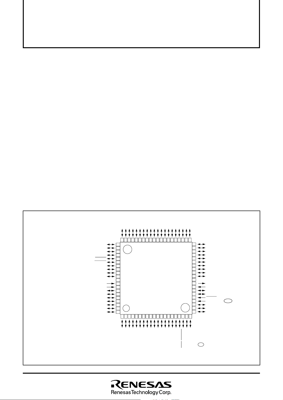
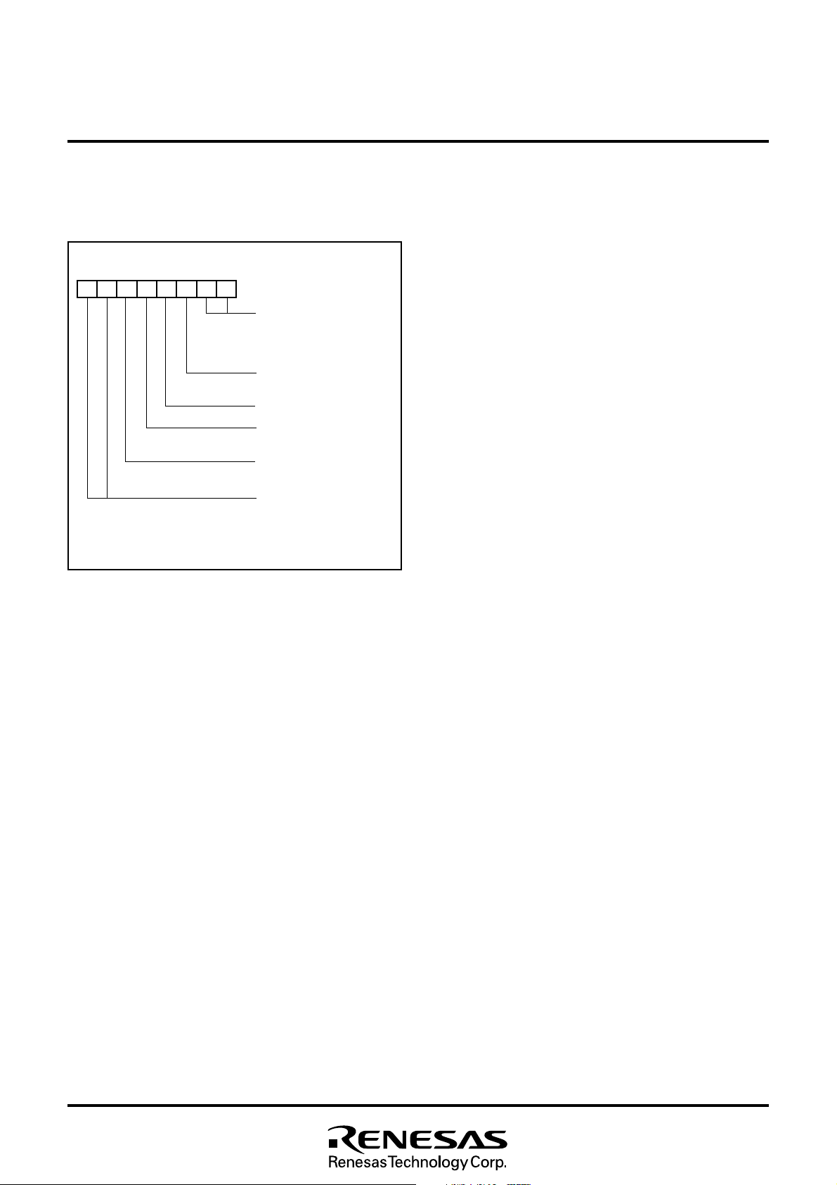
PIN CONFIGURATION (TOP VIEW)
P31/PWM10
P30/PWM00
7/SERIRQ
P8
P86/LCLK
P8
5/LRESET
P84/LFRAME
P83/LAD3
P82/LAD2
P81/LAD1
P80/LAD0
VCC
VREF
SS
AV
P67/AN7
P66/AN6
P65/AN5
P64/AN4
P63/AN3
P62/AN2
P61/AN1
0
6
3
5
2
P3
P34P3
P3
60
59
58
57
61
62
63
64
65
66
67
68
69
70
71
72
73
74
75
76
77
78
79
80
1
0
/AN
0
P6
56
M38857M8-XXXHP
M38858MC-XXXHP
M38859M8-XXXHP
M38859FFHP
5
3
2
4
31
41
CL
DA
/S
/S
7
6
/INT
/INT
4
5
P7
P7
P7
P7
2
3
1
7
P0
P3
P3
55
54
6
7
2
21
P7
/INT
3
P7
P04P05P06P07P11P12P13P14P1
P0
P0
P0
48
49
51
53
52
50
9
8
0
1
P7
P7
11
10
01
11
/PWM
/PWM
1
2
/DA
/DA
6
7
P5
P5
13
12
0
1
/CNTR
/CNTR
4
5
P5
P5
Package type : 80P6Q-A
47
14
40
/INT
3
P5
0
P1
46
15
30
/INT
2
P5
45
16
20
/INT
1
P5
44
43
17
18
5
/INT
0
P5
/CLKRUN
RDY
/S
7
P4
5
41
42
40
P16
39
P17
38
P20/CMPREF
37
P21
36
P22
35
P2
3
4(LED0)
P2
5(LED1)
P2
P26(LED2)
P27(LED3)
VSS
XOUT
XIN
P40/XCOUT
P41/XCIN
RESET
CNVSS
P42/INT0
P43/INT1
P44/RXD
: Flash memory version
VPP
19
CLK
/S
6
P4
34
33
32
31
30
29
28
27
26
25
24
23
22
21
20
XD
/T
5
P4
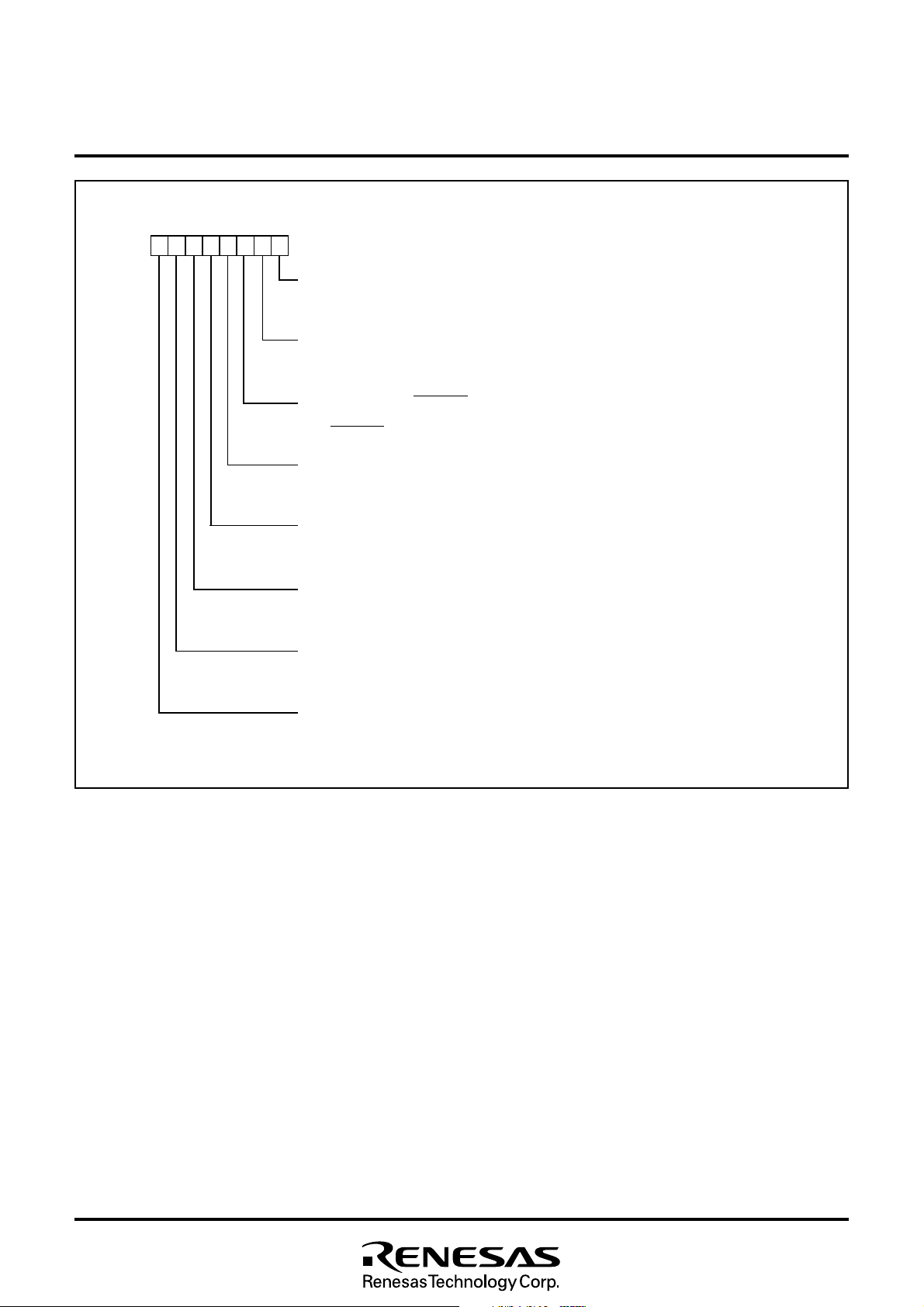
Fig. 1 Pin configuration
1
Page 3
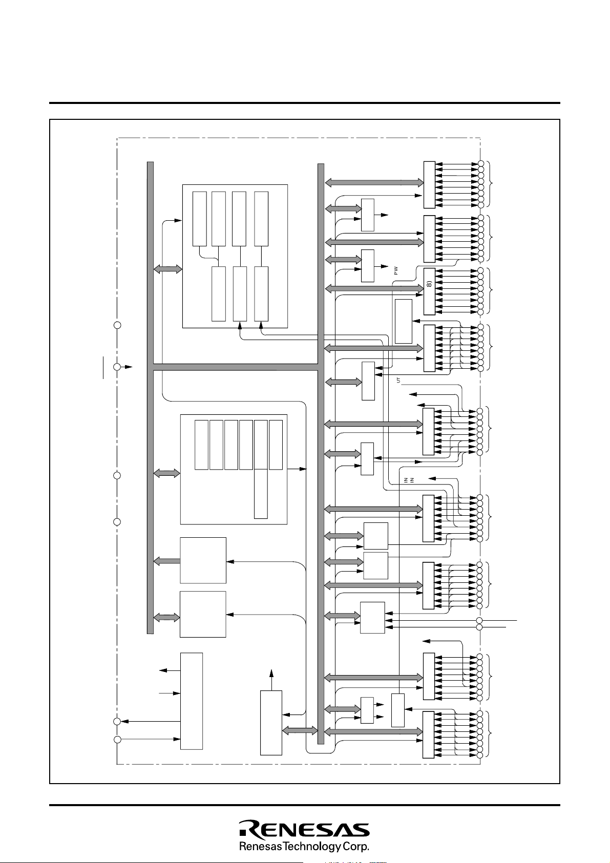
MITSUBISHI MICROCOMPUTERS
N
T
0
,
C
N T
R
0
C
N T
R
1
R
E
F
V
S
S
R
A
M
R
O
M
C
P
U
A
S
C
C
P
S
V
S
S
3
0
R
E S E
T
5
V
C
C
7
1
2
4
C
N
V
S
S
P
5 ( 8
)
P
7 ( 8
)
2
6
3
7
P
8 ( 8
)
P
6 ( 8
)
7
4
7
6
8
8
0
7
5
7
7
9
1
7
2
3
I
N
2
8
9
S
I / O ( 8
)
D
-
A
c
o n v e r t e r
2
(
8
)
e
s
e
t
i
n
p
u
t
C
l o c k g e n e r a t i n g c i r c u i
t
a
i
n
-
c
l
o
c
k
n
p
u
t
M
a i n - c l o c
k
o
u t p u
t
A
-
D
c
o
n
v
e
r
t
e
r
(
1
0
)
T
i m e r Y ( 8
)
T
i m e r X ( 8
)
P
r e s c a l e r 1 2 ( 8
)
P
r e s c a l e r X ( 8
)
P
r e s c a l e r Y ( 8
)
T
i m e r 1 ( 8
)
T
i m e r 2 ( 8
)
I
/
O
p
o
r
t
P
5
I
/ O p o r t P
7
I
/ O p o r t P
8
I
/
O
p
o
r
t
P
6
S
u b - c l o c
k
i
n p u
t
O
U
T
X
C
I
N
C
O
U
T
S
u b - c l o c
k
o
u t p u
t
W
a t c h d o
g
t
i
m
e
r
R
e s e
t
0
(
8
)
P
1 ( 8
)
P
2 ( 8
)
P
3 ( 8
)
I
/ O p o r t P
0
/
O
p
o
r
t
P
1
I
/ O p o r t P
2
I
/ O p o r t P
3
K
e y - o n
w
a k e - u
p
C
I
N
C
O U
T
P
4 ( 8
)
/
O
p
o
r
t
P
4
C
o m p a r a t o
r
I
N
T
1
W
M
0
(
1
4
)
P
W M 1 ( 1 4
)
W
M
0
0
,
W
M
0
1
P
W
M
1
0
,
P
W
M
1
1
P
C
i
n
t
e
r
f
a
c
e
I
C
S
C
L
S
D
A
N
T
4
1
I
N
T
2
1
,
N
T
3
1
,
6
3
5
6
7
9
4
6
6
8
0
D
-
A
c
o n v e r t e r
1
(
8
)
1
0
2
4
1
6
1
3
1
5
1
7
8
2
0
2
2
6
1
9
2
1
3
2
7
5
5
7
5
9
1
6
5
8
0
2
3
1
3
5
3
7
2
4
3
6
3
8
9
4
1
3
5
0
2
4
4
6
7
8
9
5
0
5
1
2
3
4
N
T
4
0
,
I
N
T
2
0
,
I
N
T
3
0
,
N
T
5
C
L K R U
N
C
M
P
R
E
F
3885 Group
SINGLE-CHIP 8-BIT CMOS MICROCOMPUTER
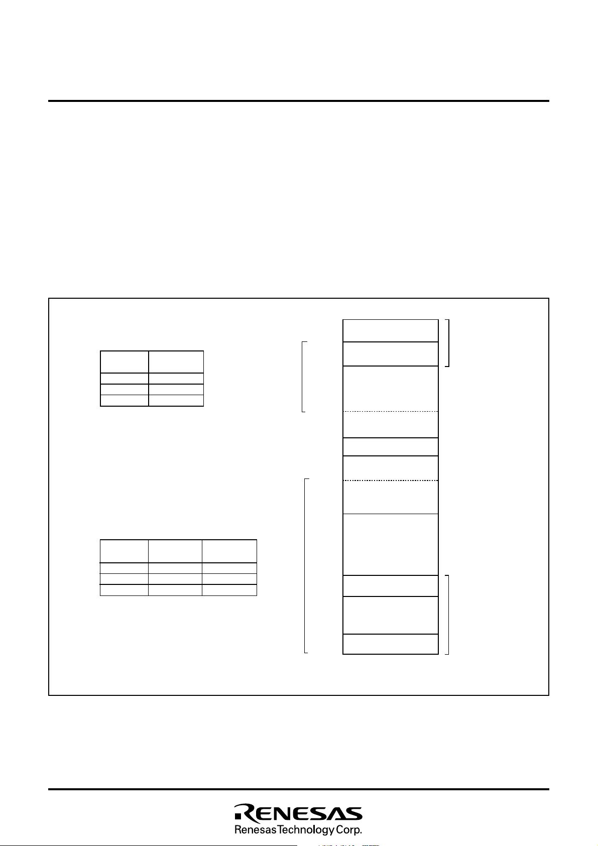
FUNCTIONAL BLOCK DIAGRAM (Package : 80P6Q-A)
Fig. 2 Functional block diagram
2
Page 4
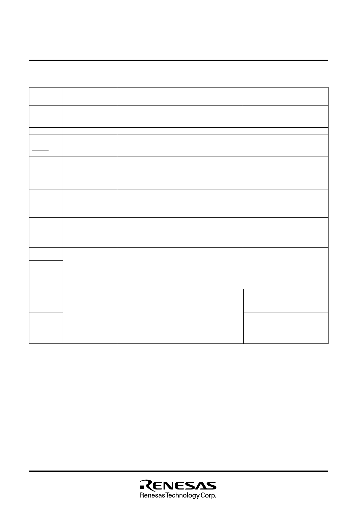
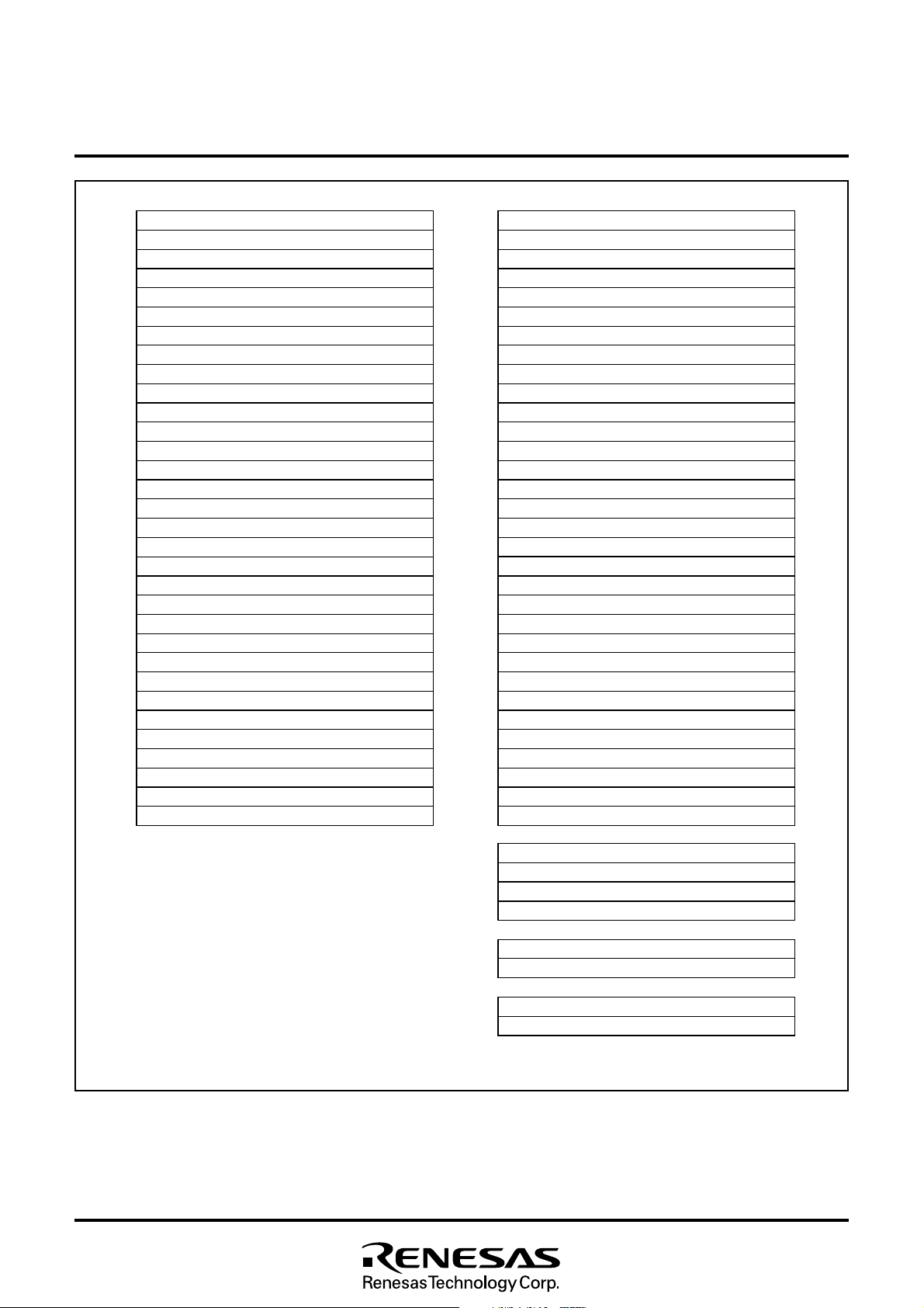
PIN DESCRIPTION
Table 1 Pin description (1)
MITSUBISHI MICROCOMPUTERS
3885 Group
SINGLE-CHIP 8-BIT CMOS MICROCOMPUTER
VCC, VSS
CNVSS
VREF
AVSS
RESET
XIN
XOUT
P00–P07
P10–P17
P20/CMPREF
P21–P27
P30/PWM00
P31/PWM10
P32–P37
NamePin
Power source
CNVSS input
Reference voltage
Analog power source
Reset input
Clock input
Clock output
I/O port P0
I/O port P1
I/O port P2
I/O port P3
Functions
•Apply voltage of 3.0 V ±10 % to Vcc, and 0 V to Vss.
•Connected to V
•In the flash memory version, this pin functions as the V
•Reference voltage input pin for A-D and D-A converters.
•Analog power source input pin for A-D and D-A converters.
•Connect to V
•Reset input pin for active “L”.
•Input and output pins for the clock generating circuit.
•Connect a ceramic resonator or quartz-crystal oscillator between the XIN and XOUT pins to set
the oscillation frequency.
•When an external clock is used, connect the clock source to the XIN pin and leave the XOUT
pin open.
•8-bit I/O port.
•I/O direction register allows each pin to be individually programmed as either input or output.
•CMOS compatible input level.
•CMOS 3-state output structure or N-channel open-drain output structure.
•8-bit I/O port.
•I/O direction register allows each pin to be individually programmed as either input or output.
•CMOS compatible input level.
•CMOS 3-state output structure or N-channel open-drain output structure.
•8-bit I/O port.
•I/O direction register allows each pin to be individually
programmed as either input or output.
•CMOS compatible input level.
•CMOS 3-state output structure.
•P24 to P27 (4 bits) are enabled to output large current for LED drive.
•8-bit I/O port.
•I/O direction register allows each pin to be individually
programmed as either input or output.
•CMOS compatible input level.
•CMOS 3-state output structure.
•These pins function as key-on wake-up and compara-
tor input.
•These pins are enabled to control pull-up.
SS.
SS.
Function except a port function
PP power source input pin.
•Comparator reference power source
input pin
•Key-on wake-up input pins
•Comparator input pins
•PWM output pins
•Key-on wake-up input pins
•Comparator input pins
3
Page 5
Table 2 Pin description (2)
MITSUBISHI MICROCOMPUTERS
3885 Group
SINGLE-CHIP 8-BIT CMOS MICROCOMPUTER
P4
0/XCOUT
P41/XCIN
P42/INT0
P43/INT1
P44/RxD
P45/TxD
P46/SCLK
P47/SRDY
/CLKRUN
P50/INT5
P51/INT20
P52/INT30
P53/INT40
P54/CNTR0
P55/CNTR1
P56/DA1/PWM01
P57/DA2/PWM11
P60/AN0–P67/AN
P70
P71
P72
P73/INT21
P74/INT31
P75/INT41
P76/SDA
P77/SCL
P80/LAD0
P81/LAD1
P82/LAD2
P83/LAD3
P84/LFRAME
P85/LRESET
P86/LCLK
P87/SERIRQ
I/O port P4
I/O port P5
7
I/O port P6
I/O port P7
I/O port P8
NamePin
•8-bit I/O port with the same function as port P0
<Input level>
CMOS compatible input level
<Output level>
P40, P41 : CMOS 3-state output structure
P42-P47 : CMOS 3-state output structure or N-
channel open-drain output structure
•Each pin level of P42 to P46 can be read even in
output port mode.
•8-bit I/O port with the same function as port P0
•CMOS compatible input level
•CMOS 3-state output structure
•8-bit I/O port with the same function as port P0
•CMOS compatible input level.
•CMOS 3-state output structure.
•8-bit CMOS I/O port with the same function as port P0
<Input level>
P70–P75 : CMOS compatible input level or
TTL compatible input level
P76, P77 : CMOS compatible input level or
SMBUS input level in the I2C-BUS
interface function,
<Output structure>
N-channel open-drain output structure
•Each pin level of P70 to P75 can be read evev in
output port mode.
•8-bit CMOS I/O port with the same function as port
P0
•CMOS compatible input level.
•CMOS 3-state output structure.
Functions
Function except a port function
•Sub-clock generating circuit I/O
pins (Connect a resonator.)
•Interrupt input pins
•Serial I/O function pins
•Serial I/O function pins
•Serialized IRQ function pin
•Interrupt input pins
•Timer X, timer Y function pins
•D-A converter output pins
•PWM output pins
•A-D converter output pins
•Interrupt input pins
•I2C-BUS interface function pins
•LPC interface function pins
•Serialized IRQ function pin
4
Page 6
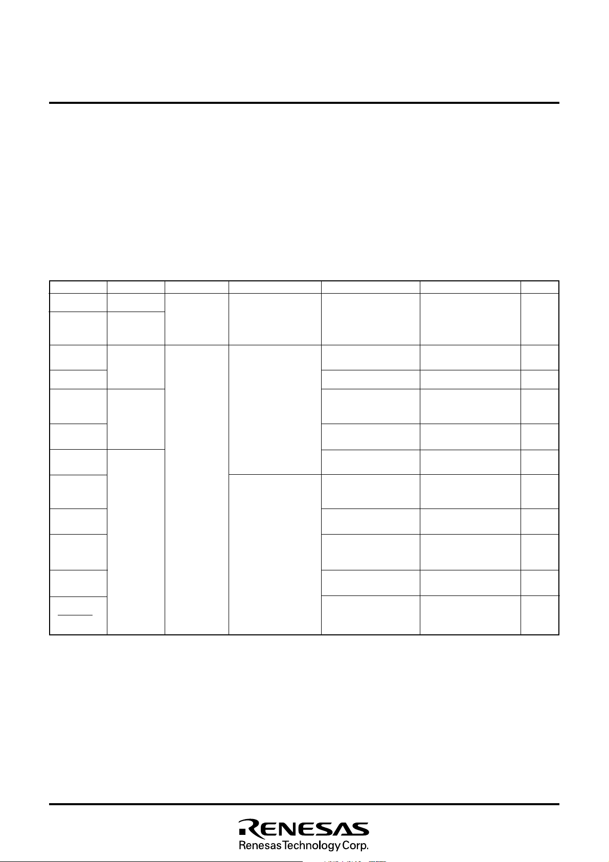
PART NUMBERING
MITSUBISHI MICROCOMPUTERS
3885 Group
SINGLE-CHIP 8-BIT CMOS MICROCOMPUTER
Product name
M3885 8 M C -XXX HP
Package type
HP : 80P6Q-A
ROM number
Omitted in the flash memory version.
ROM/Flash memory size
1
: 4096 bytes
2
: 8192 bytes
3
: 12288 bytes
4
: 16384 bytes
5
: 20480 bytes
6
: 24576 bytes
7
: 28672 bytes
8
: 32768 bytes
The first 128 bytes and the last 2 bytes of ROM are reserved
areas ; user cannot use those bytes.
However, they can be programmed or erased in the flash
memory version, so that the users can use them.
9: 36864 bytes
A: 40960 bytes
B: 45056 bytes
C: 49152 bytes
D: 53248 bytes
E: 57344 bytes
F: 61440 bytes
Fig. 3 Part numbering
Memory type
M
: Mask ROM version
F
: Flash memory version
RAM size
: 192 bytes
0
: 256 bytes
1
: 384 bytes
2
: 512 bytes
3
: 640 bytes
4
: 768 bytes
5
: 896 bytes
6
: 1024 bytes
7
: 1536 bytes
8
: 2048 bytes
9
5
Page 7
MITSUBISHI MICROCOMPUTERS
3885 Group
SINGLE-CHIP 8-BIT CMOS MICROCOMPUTER
GROUP EXPANSION
Mitsubishi plans to expand the 3885 group as follows.
Memory Type
Support for mask ROM, flash memory version.
Memory Size
ROM size ........................................................... 32 K to 60 K bytes
RAM size ..........................................................1024 to 2048 bytes
Memory Expansion
ROM size (bytes)
ROM
external
60K
56K
48K
40K
Packages
80P6Q-A ..................................0.5 mm-pitch plastic molded LQFP
M38859FF
M38858MC
Fig. 4 Memory expansion plan
Table 3 Products plan list
Product name
M38857M8-XXXHP
M38858MC-XXXHP
M38859M8-XXXHP
M38859FFHP
(P) ROM size (bytes)
ROM size for User in ( )
32768 (32638)
49152 (19022)
32768 (32638)
32K
24K
16K
8K
61440
256 512 768
RAM size (bytes)
1024
1536
2048
2048
M38857M8
1024 1280 1536 1792 2048
RAM size (bytes)
Package
80P6Q-A
Mask ROM version
Flash memory version
M38859M8
As of May 2002
Remarks
6
Page 8
MITSUBISHI MICROCOMPUTERS
3885 Group
SINGLE-CHIP 8-BIT CMOS MICROCOMPUTER
FUNCTIONAL DESCRIPTION
CENTRAL PROCESSING UNIT (CPU)
The 3885 group uses the standard 740 Family instruction set. Refer to the table of 740 Family addressing modes and machine
instructions or the 740 Family Software Manual for details on the
instruction set.
Machine-resident 740 Family instructions are as follows:
The FST and SLW instructions cannot be used.
The STP, WIT, MUL, and DIV instructions can be used.
[Accumulator (A)]
The accumulator is an 8-bit register. Data operations such as data
transfer, etc., are executed mainly through the accumulator.
[Index Register X (X)]
The index register X is an 8-bit register. In the index addressing
modes, the value of the OPERAND is added to the contents of
register X and specifies the real address.
[Index Register Y (Y)]
The index register Y is an 8-bit register. In partial instruction, the
value of the OPERAND is added to the contents of register Y and
specifies the real address.
[Stack Pointer (S)]
The stack pointer is an 8-bit register used during subroutine calls
and interrupts. This register indicates start address of stored area
(stack) for storing registers during subroutine calls and interrupts.
The low-order 8 bits of the stack address are determined by the
contents of the stack pointer. The high-order 8 bits of the stack address are determined by the stack page selection bit. If the stack
page selection bit is “0” , the high-order 8 bits becomes “0016”. If
the stack page selection bit is “1”, the high-order 8 bits becomes
“0116”.
The operations of pushing register contents onto the stack and
popping them from the stack are shown in Figure 7.
Store registers other than those described in Figure 7 with program when the user needs them during interrupts or subroutine
calls.
[Program Counter (PC)]
The program counter is a 16-bit counter consisting of two 8-bit
registers PCH and PCL. It is used to indicate the address of the
next instruction to be executed.
b7
b0
A Accumulator
b7
b0
X Index register X
b7
b0
Y Index register Y
b7 b0
S Stack pointer
b7b15 b0
H
PC
L
Program counterPC
b7 b0
N V T B D I Z C Processor status register (PS)
Carry flag
Zero flag
Interrupt disable flag
Decimal mode flag
Break flag
Index X mode flag
Overflow flag
Negative flag
Fig. 5 740 Family CPU register structure
7
Page 9
On-going Routin
e
MITSUBISHI MICROCOMPUTERS
3885 Group
SINGLE-CHIP 8-BIT CMOS MICROCOMPUTER
P u s h r e t u r n a d d r e s s
o n s t a c k
P O P re t u r n
a d d r e s s f r o m s t a c k
I n t e r r u p t r e q u e s t
M (S) (PCH)
( S )
M ( S )( P CL)
(S)
S u b r o u t i n e
E x e c u t e R T S
( S )
( P CL)M ( S )
( S )
( P CH)M ( S )
( S ) – 1
(S)– 1
( S ) + 1
( S ) + 1
( N o t e )
E x e c u t e J S R
M (S) (PCH)
(S)
(S) – 1
M (S) (PCL)
(S)
(S) – 1
M ( S )( P S )
(S)
(S) – 1
I n t e r r u p t
S e r v i c e R o u t i n e
E x e c u t e R T I
(S)
(S) + 1
( P S )M ( S )
(S)
(S) + 1
(PCL)M (S)
(S)
(S) + 1
Push return address
on stack
Push contents of processor
status register on stack
I Flag is set from “0” to “1”
Fetch the jump vector
POP contents of
processor status
register from stack
POP return
address
from stack
(PCH)M (S)
N o t e: C o n d i t i o n f o r a c c e p t a n c e o f a n i n t e r r u p t I n t e r r u p t e n a b l e f l a g i s “ 1 ”
Fig. 6 Register push and pop at interrupt generation and subroutine call
Table 4 Push and pop instructions of accumulator or processor status register
Push instruction to stack
Accumulator
Processor status register
Interrupt disable flag is “0”
PHA
PHP
Pop instruction from stack
PLA
PLP
8
Page 10

MITSUBISHI MICROCOMPUTERS
3885 Group
SINGLE-CHIP 8-BIT CMOS MICROCOMPUTER
[Processor status register (PS)]
The processor status register is an 8-bit register consisting of 5
flags which indicate the status of the processor after an arithmetic
operation and 3 flags which decide MCU operation. Branch operations can be performed by testing the Carry (C) flag , Zero (Z) flag,
Overflow (V) flag, or the Negative (N) flag. In decimal mode, the Z,
V, N flags are not valid.
•Bit 0: Carry flag (C)
The C flag contains a carry or borrow generated by the arithmetic
logic unit (ALU) immediately after an arithmetic operation. It can
also be changed by a shift or rotate instruction.
•Bit 1: Zero flag (Z)
The Z flag is set if the result of an immediate arithmetic operation
or a data transfer is “0”, and cleared if the result is anything other
than “0”.
•Bit 2: Interrupt disable flag (I)
The I flag disables all interrupts except for the interrupt
generated by the BRK instruction.
Interrupts are disabled when the I flag is “1”.
•Bit 3: Decimal mode flag (D)
The D flag determines whether additions and subtractions are
executed in binary or decimal. Binary arithmetic is executed when
this flag is “0”; decimal arithmetic is executed when it is “1”.
Decimal correction is automatic in decimal mode. Only the ADC
•Bit 4: Break flag (B)
The B flag is used to indicate that the current interrupt was
generated by the BRK instruction. The BRK flag in the processor
status register is always “0”. When the BRK instruction is used to
generate an interrupt, the processor status register is pushed
onto the stack with the break flag set to “1”.
•Bit 5: Index X mode flag (T)
When the T flag is “0”, arithmetic operations are performed
between accumulator and memory. When the T flag is “1”, direct
arithmetic operations and direct data transfers are enabled
between memory locations.
•Bit 6: Overflow flag (V)
The V flag is used during the addition or subtraction of one byte
of signed data. It is set if the result exceeds +127 to -128. When
the BIT instruction is executed, bit 6 of the memory location
operated on by the BIT instruction is stored in the overflow flag.
•Bit 7: Negative flag (N)
The N flag is set if the result of an arithmetic operation or data
transfer is negative. When the BIT instruction is executed, bit 7 of
the memory location operated on by the BIT instruction is stored
in the negative flag.
Table 5 Set and clear instructions of each bit of processor status register
Set instruction
Clear instruction
C flag
SEC
CLC
Z flag
–
–
I flag
SEI
CLI
D flag
SED
CLD
B flag
–
–
T flag
SET
CLT
V flag
–
CLV
N flag
–
–
9
Page 11
[CPU Mode Register (CPUM)] 003B16
The CPU mode register contains the stack page selection bit, etc.
The CPU mode register is allocated at address 003B16.
MITSUBISHI MICROCOMPUTERS
3885 Group
SINGLE-CHIP 8-BIT CMOS MICROCOMPUTER
b 7
1
b 0
C P U m o d e r e g i s t e r
(
C P U M : a d d r e s s
P r o c e s s o r m o d e b i t s
b 1 b 0
0 0 : S i n g l e - c h i p m o d e
0 1 : N o t a v a i l a b l e
1 0 : N o t a v a i l a b l e
1 1 : N o t a v a i l a b l e
S t a c k p a g e s e l e c t i o n b i t
0 : 0 p a g e
1 : 1 p a g e
F i x t h i s b i t t o “ 1 ” .
P o r t P 4
0 : I / O p o r t f u n c t i o n ( s t o p o s c i l l a t i n g )
1 : X
M a i n c l o c k ( X
0 : O s c i l l a t i n g
1 : S t o p p e d
M a i n c l o c k d i v i s i o n r a t i o s e l e c t i o n b i t s
b 7 b 6
0 0 : φ = f ( X
0 1 : φ = f ( X
1 0 : φ = f ( X
1 1 : N o t a v a i l a b l e
Fig. 7 Structure of CPU mode register
0
/ P 41 s w i t c h b i t
C I N
– X
C O U T
0 0 3 B
1 6
)
o s c i l l a t i n g f u n c t i o n
I N
– X
O U T
) s t o p b i t
I N
) / 2 ( h i g h - s p e e d m o d e )
I N
) / 8 ( m i d d l e - s p e e d m o d e )
C I N
) / 2 ( l o w - s p e e d m o d e )
10
Page 12
MITSUBISHI MICROCOMPUTERS
3885 Group
SINGLE-CHIP 8-BIT CMOS MICROCOMPUTER
MEMORY
RAM
RAM is used for data storage and for stack area of subroutine
calls and interrupts.
ROM
ROM is used for program code and data table storage.
The first 128 bytes and the last 2 bytes of ROM are reserved for
device testing code and the rest is user area. Programming/Erasing of the reserved ROM area is possible in the flash memory
version.
R A M a r e a
R A M s i z e
( b y t e s )
1 0 2 4
1 5 3 6
2 0 4 8
A d d r e s s
X X X X
0 4 3 F
0 6 3 F
0 8 3 F
1 6
1 6
1 6
1 6
R A M
Zero Page
Access to this area with only 2 bytes is possible in the zero page
addressing mode.
Special Page
Access to this area with only 2 bytes is possible in the special
page addressing mode.
Interrupt Vector Area
The interrupt vector area contains reset and interrupt vectors.
Special Function Register (SFR) Area
The special function register area contains the control registers
such as I/O ports, timers, serial I/O, etc.
0000
0040
0100
XXXX
16
16
16
16
S F R a r e a
Z e r o p a g e
R O M a r e a
R O M s i z e
( b y t e s )
3 2 7 6 8
4 9 1 5 2
6 1 4 4 0
Fig. 8 Memory map diagram
A d d r e s s
Y Y Y Y
8 0 0 0
4 0 0 0
1 0 0 0
Not used
0FF0
0 F F F
Y Y Y Y
16
1 6
1 6
SFR area
R e s e r v e d R O M a r e a
( N o t e )
( 1 2 8 b y t e s )
ZZZZ
16
A d d r e s s
1 6
1 6
1 6
1 6
Z Z Z Z
8 0 8 0
4 0 8 0
1 0 8 0
1 6
1 6
1 6
1 6
ROM
FF00
16
FFDC
16
I n t e r r u p t v e c t o r a r e a
FFFE
16
Reserved ROM area
FFFF
16
Notes: This area is reserv ed in the mask ROM version.
This area is usable in f las h memory version.
(Note)
Special page
11
Page 13
MITSUBISHI MICROCOMPUTERS
3885 Group
SINGLE-CHIP 8-BIT CMOS MICROCOMPUTER
P o r t P 0 ( P 0 )
0000
16
P o r t P 0 d i r e c t i o n r e g i s t e r ( P 0 D )
0 0 0 1
1 6
P o r t P 1 ( P 1 )
0 0 0 2
1 6
P o r t P 1 d i r e c t i o n r e g i s t e r ( P 1 D )
0 0 0 3
1 6
P o r t P 2 ( P 2 )
0 0 0 4
1 6
P o r t P 2 d i r e c t i o n r e g i s t e r ( P 2 D )
0 0 0 5
1 6
P o r t P 3 ( P 3 )
0 0 0 6
1 6
P o r t P 3 d i r e c t i o n r e g i s t e r ( P 3 D )
0 0 0 7
1 6
P o r t P 4 ( P 4 )
0 0 0 8
1 6
P o r t P 4 d i r e c t i o n r e g i s t e r ( P 4 D )
0 0 0 9
1 6
P o r t P 5 ( P 5 )
0 0 0 A
1 6
P o r t P 5 d i r e c t i o n r e g i s t e r ( P 5 D )
0 0 0 B
1 6
P o r t P 6 ( P 6 )
0 0 0 C
1 6
P o r t P 6 d i r e c t i o n r e g i s t e r ( P 6 D )
0 0 0 D
1 6
P o r t P 7 ( P 7 )
0 0 0 E
1 6
P o r t P 7 d i r e c t i o n r e g i s t e r ( P 7 D )
0 0 0 F
1 6
Port P8 (P8)/Port P4 in put register (P4I)
0 0 1 0
1 6
0 0 1 1
1 6
Port P8 direction register (P8D)/Port P7 input register (P7I)
0012
0013
0 0 1 4
0 0 1 5
0016
0017
0 0 1 8
0 0 1 9
001A
001B
0 0 1 C
0 0 1 D
0 0 1 E
001F
2
16
I
C d a t a s h i f t r e g i s t e r ( S 0 )
2
16
I
C a d d r e s s r e g i s t e r ( S 0 D )
2
1 6
I
C status register ( S 1)
2
1 6
I
C control register (S1D)
2
16
I
C c l o c k c o n t r o l r e g i s t e r ( S 2 )
2
16
I
C s t a r t / s t o p c o n d i t i o n c o n t r o l r e g i s t e r ( S 2 D )
Transmit/Receiv e buffer register (TB/RB)
1 6
Serial I/O status re gister (SIOSTS)
1 6
S e r i a l I / O c o n t r o l r e g i s t e r ( S I O C O N )
16
U A R T c o n t r o l r e g i s t e r ( U A R T C O N )
16
Baud rate generator ( B RG)
1 6
S e r i a l i z e d I R Q c o n t r o l r e g i s t e r ( S E R C O N )
1 6
W a t c h d o g t i m e r c o n t r o l r e g i s t e r ( W D T C O N )
1 6
S e r i a l i z e d I R Q r e q u e s t r e g i s t e r ( S E R I R Q )
16
0020
0021
0022
0023
0024
0025
0026
0027
0028
0029
002A
002B
002C
002D
002E
0 0 2 F
0030
0031
0032
0033
0034
0035
0036
0037
0038
0039
003A
003B
003C
003D
003E
003F
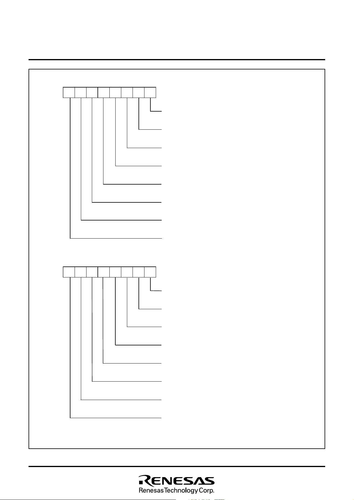
P r e s c a l e r 1 2 ( P R E 1 2 )
16
T i m e r 1 ( T 1 )
16
T i m e r 2 ( T 2 )
16
T i m e r X Y m o d e r e g i s t e r ( T M )
16
P r e s c a l e r X ( P R E X )
16
T i m e r X ( T X )
16
P r e s c a l e r Y ( P R E Y )
16
T i m e r Y ( T Y )
16
D a t a b a s b u f f e r r e g i s t e r 0 ( D B B 0 )
16
D a t a b a s b u f f e r s t a t u s r e g i s t e r 0 ( D B B S T S 0 )
16
L P C c o n t r o l r e g i s t e r ( L P C C O N )
16
D a t a b a s b u f f e r r e g i s t e r 1 ( D B B 1 )
16
D a t a b a s b u f f e r s t a t u s r e g i s t e r 1 ( D B B S T S 1 )
16
C o m p a r a t o r d a t a r e g i s t e r ( C M P D )
16
P o r t c o n t r o l r e g i s t e r 1 ( P C T L 1 )
16
P o r t c o n t r o l r e g i s t e r 2 ( P C T L 2 )
1 6
P W M 0 H r e g i s t e r ( P W M 0 H )
16
P W M 0 L r e g i s t e r ( P W M 0 L )
16
PWM1H register (PWM1H)
16
PWM1L register (PWM1L)
16
AD/DA control regi s ter (ADCON)
16
A - D c o n v e r s i o n r e g i s t e r 1 ( A D 1 )
16
D - A 1 c o n v e r s i o n r e g i s t e r ( D A 1 )
16
D-A2 conversion register (DA2)
16
A-D conversion regis ter 2 (AD2)
16
I n t e r r u p t s o u r c e s e l e c t i o n r e g i s t e r ( I N T S E L )
16
I n t e r r u p t e d g e s e l e c t i o n r e g i s t e r ( I N T E D G E )
16
C P U m o d e r e g i s t e r ( C P U M )
16
Interrupt request register 1 (IREQ1)
16
I n t e r r u p t r e q u e s t r e g i s t e r 2 ( I R E Q 2 )
16
I n t e r r u p t c o n t r o l r e g i s t e r 1 ( I C O N 1 )
16
I n t e r r u p t c o n t r o l r e g i s t e r 2 ( I C O N 2 )
16
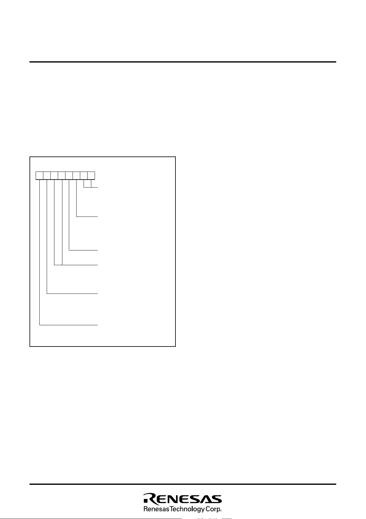
Fig. 9 Memory map of special function register (SFR)
12
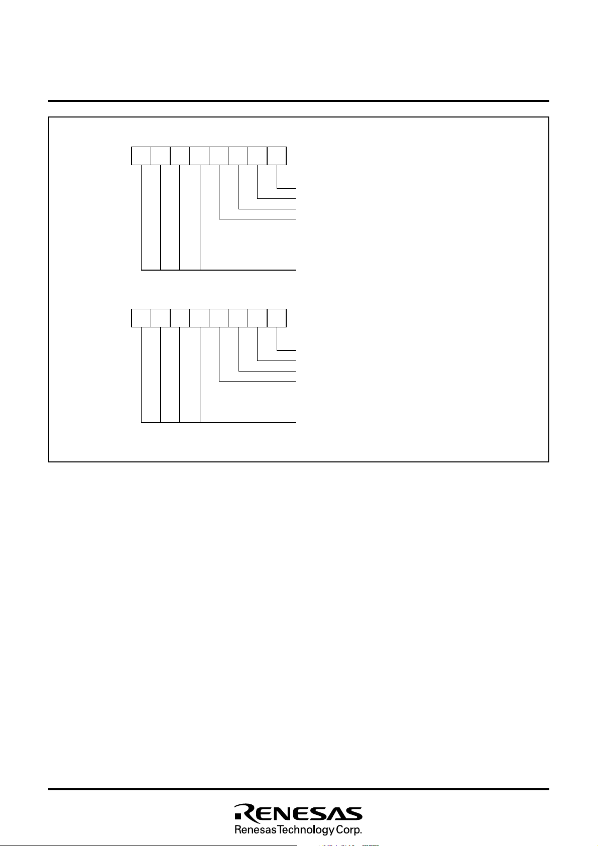
LPC0 address register L ( LP C0ADL)
0 F F 0
1 6
0FF1
0FF2
0FF8
0FFE
L P C 0 a d d r e s s r e g i s t e r H ( L P C 0 A D H )
16
L P C 1 a d d r e s s r e g i s t e r L ( L P C 1 A D L )
16
LPC1 address regist er H ( LP C1ADH)
0FF3
16
16
P o r t P 5 i n p u t r e g i s t e r ( P 5 I )
P o r t c o n t r o l r e g i s t e r 3 ( P C T L 3 )
0FF9
16
F l a s h m e m o r y c o n t r o l r e g i s t e r ( F M C R )
16
0FFF16Reserved
N o t e : T h i s a p p l i e s t o o n l y f l a s h m e m o r y v e r s i o n .
(Note)
(Note)
Page 14
MITSUBISHI MICROCOMPUTERS
3885 Group
SINGLE-CHIP 8-BIT CMOS MICROCOMPUTER
I/O PORTS
All I/O pins are programmable as input or output. All I/O ports
have direction registers which specify the data direction of each
pin like input/output. One bit in a direction register corresponds to
one pin. Each pin can be set to be input or output port.
Writing “0” to the bit corresponding to the pin, that pin becomes an
input mode. Writing “1” to the bit, that pin becomes an output
mode.
When the data is read from the bit of the port register corresponding to the pin which is set to output, the value shows the port latch
data, not the input level of the pin. When a pin set to input, the pin
Table 6 I/O port function (1)
Pin
P00-P07
P10–P17
P20/CMPREF
P21–P27
P30/PWM00
P31/PWM10
P32–P37
P40/XCOUT
P41/XCIN
P42/INT0
P43/INT1
P44/RXD
P45/TXD
P46/SCLK (13)
P47/SRDY
/CLKRUN
Name
Port P0
Port P1
Port P2
Port P3
Port P4
Input/Output
Input/output,
individual bits
I/O Structure Non-Port Function
CMOS compatible
input level
CMOS 3-state output
or N-channel opendrain output
CMOS compatible
input level
CMOS 3-state output
CMOS compatible
input level
CMOS 3-state output
or N-channel opendrain output
comes floating. In input port mode, writing the port register
changes only the data of the port latch and the pin remains high
impedance state.
When the P8 function selection bit of the port control register 2 is
set to “1”, reading from address 001016 reads the port P4 register,
and reading from address 001116 reads the port P7 register.
Especially, the input level of P42 to P46 pins and P70 to P75 pins
can be read regardless of the data of the direction registers in this
case.
Related SFRs
Port control register 1 (1)
Analog comparator
power source input pin
PWM output
Key-on wake up input
Comparator input
Key-on wake up input
Comparator input
Sub-clock generating
circuit
External interrupt input
Serial I/O function input
Serial I/O function output
Serial I/O function I/O
Serial I/O function output
Serialized IRQ function
output
Port control register 1
Port control register 2
Port control register 1
AD/DA control register
Port control register 1
CPU mode register
Interrupt edge selection
register
Port control register 2
Serial I/O control register
Port control register 2
Serial I/O control register
UART control register
Port control register 2
Serial I/O control register
Port control register 2
Serial I/O control register
Serialized IRQ control
register
Ref.No.
(2)
(3)
(4)
(5)
(6)
(7)
(8)
(9)
(10)
(11)
(12)
(14)
13
Page 15
Table 7 I/O port function (2)
Pin
P50/INT5
P51/INT20
P52/INT30
P53/INT40
P54/CNTR0
P55/CNTR1
Name
Port P5
MITSUBISHI MICROCOMPUTERS
3885 Group
SINGLE-CHIP 8-BIT CMOS MICROCOMPUTER
Input/Output I/O Format Non-Port Function Ref.No.
CMOS compatible
input level
CMOS 3-state output
or N-channel
opendrain output
External interrupt input
Timer X, timer Y function I/O
Related SFRs
Interrupt edge selection
register
Timer XY mode register
(15)
(16)
(17)
P56/DA1/
PWM01
P57/DA2/
PWM11
P60/AN0–
P67/AN7
P70
P71
P72
P73/INT21
P74/INT31
P75/INT41
P76/SDA
P77/SCL
P80/LAD0
P81/LAD1
P82/LAD2
P83/LAD3
P84/
LFRAME
P85/
LRESET
P86/LCLK
P87/
SERIRQ
Notes1: For details usage of double-function ports as function I/O ports, refer to the applicable sections.
2: Make sure that the input level of each pin should be either 0 V or V
When an input level is at an intermediate voltage level, the I
Port P6
Input/output,
individual bits
Port P7
Port P8
CMOS compatible
input level
CMOS 3-state output
CMOS compatible
input level or
TTL input level
Pure N-channel
open-drain output
CMOS compatible
input level or SMBUS
input level
Pure N-channel
open-drain output
CMOS compatible
input level
CMOS 3-state output
CC in STP mode.
CC current will become large because of the input buffer gate.
D-A converter output
PWM output
A-D converter input AD/DA control register
External interrupt input
I2C-BUS interface function I/O
LPC interface function
I/O
Serialized IRQ function
I/O
AD/DA control register
UART control register
Port control register 2
Interrupt edge selection
register
Port control register 2
I2C control register
Data bus buffer control
register
(18)
(19)
(20)
(21)
(22)
(23)
(24)
(25)
(26)
(27)
(28)
14
Page 16
MITSUBISHI MICROCOMPUTERS
g
3885 Group
SINGLE-CHIP 8-BIT CMOS MICROCOMPUTER
( 1 ) P o r t s P 0 , P 1
P 00– P 03,
P 04– P 07,
P 10– P 13,
P 14– P 1
7
D a t a b u s
( 3 ) P o r t P21– P 2
D a t a b u s
o u t p u t s t r u c t u r e
s e l e c t i o n b i t s
D i r e c t i o n
r e g i s t e r
P o r t l a t c h
7
i s t e
D i r e c t i o n
r
r e
P o r t l a t c h
( 2 ) P o r t P 2
D a t a b u s
( 4 ) P o r t s P 30, P 3
P W M0 ( P W M1) o u t p u t p i n s e l e c t i o n b i t
D a t a b u s
0
D i r e c t i o n
r e g i s t e r
P o r t l a t c h
C o m p a r a t o r r e f e r e n c e p o w e r s o u r c e i n p u t
1
PWM
0
(PWM1) enable bit
Direction
register
P o r t l a t c h
00
(PWM10) output
PWM
C o m p a r a t o r r e f e r e n c e i n p u t
P 3
0
– P 33 p u l l - u p c o n t r o l b i t
Comparator input
Key-on wake-up input
p i n s e l e c t b i t
( 5 ) P o r t s P 32– P 3
D a t a b u s
(7) Port P4
D a t a b u s
1
P o r t XC s w i t c h b i t
7
P30–P33,
P3
4
–P3
7
pull-up control bit
D i r e c t i o n
r e g i s t e r
P o r t l a t c h
Key-on wake-up input
D i r e c t i o n
r e g i s t e r
P o r t l a t c h
S u b - c l o c k o s c i l l a t i o n c i r c u i t
C o m p a r a t o r i n p u t
( 6 ) P o r t P 4
D a t a b u s
0
Port XC switch bit
D i r e c t i o n
r e g i s t e r
P o r t l a t c h
(8) Ports P42 , P4
P 4 o u t p u t s t r u c t u r e s e l e c t i o n b i t
D i r e c t i o n
Data bus
Port latch
3
r e g i s t e r
Sub-clock oscillation circuit
I n t e r r u p t i n p u t
✻1
Port P4
P o r t X
1
C
s w i t c h b i t
✻1 . R e a d i n g t h e p o r t P 8 r e g i s t e r ( a d d r e s s 0 0 1 0
r e g i s t e r 2 ( P C T L 2 ) .
1 6
) i s s w i t c h e d t o p o r t P 4 p i n i n p u t l e v e l b y t h e P 8 f u n c t i o n s e l e c t i o n b i t o f t h e p o r t c o n t r o l
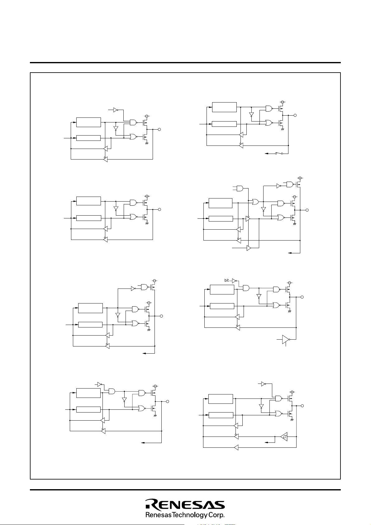
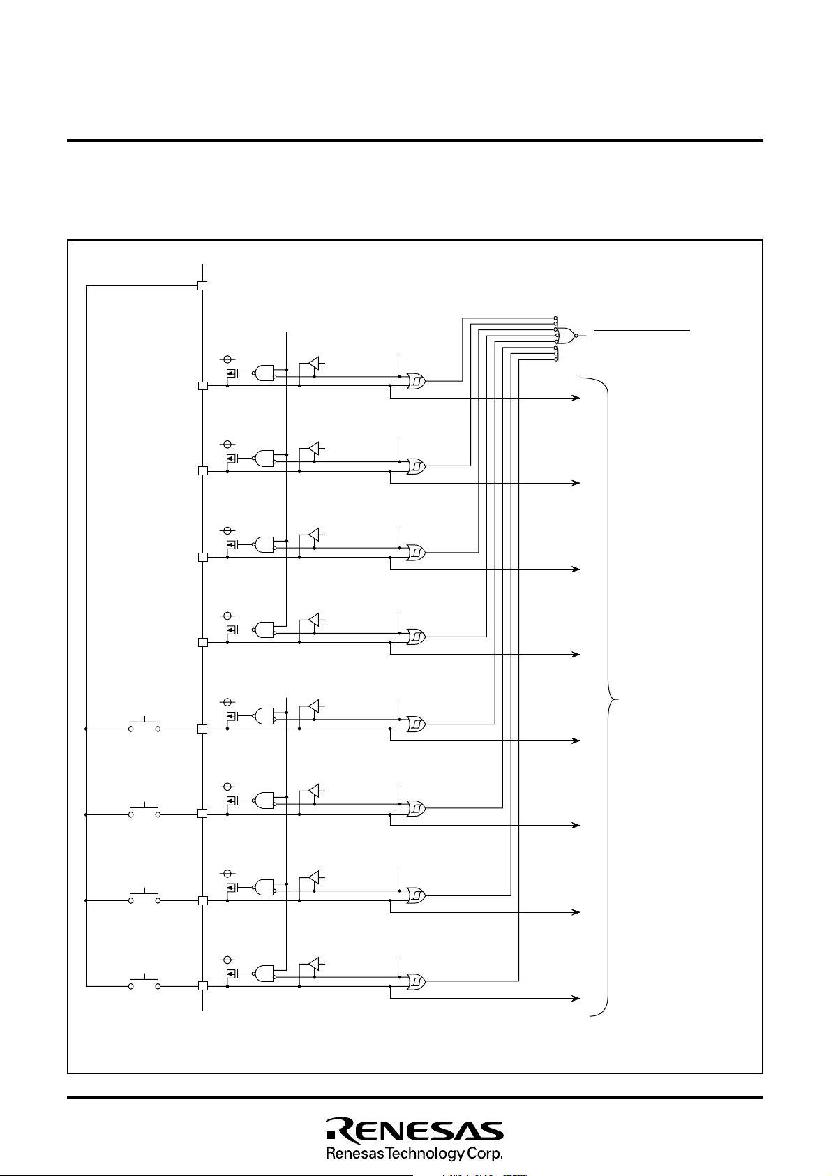
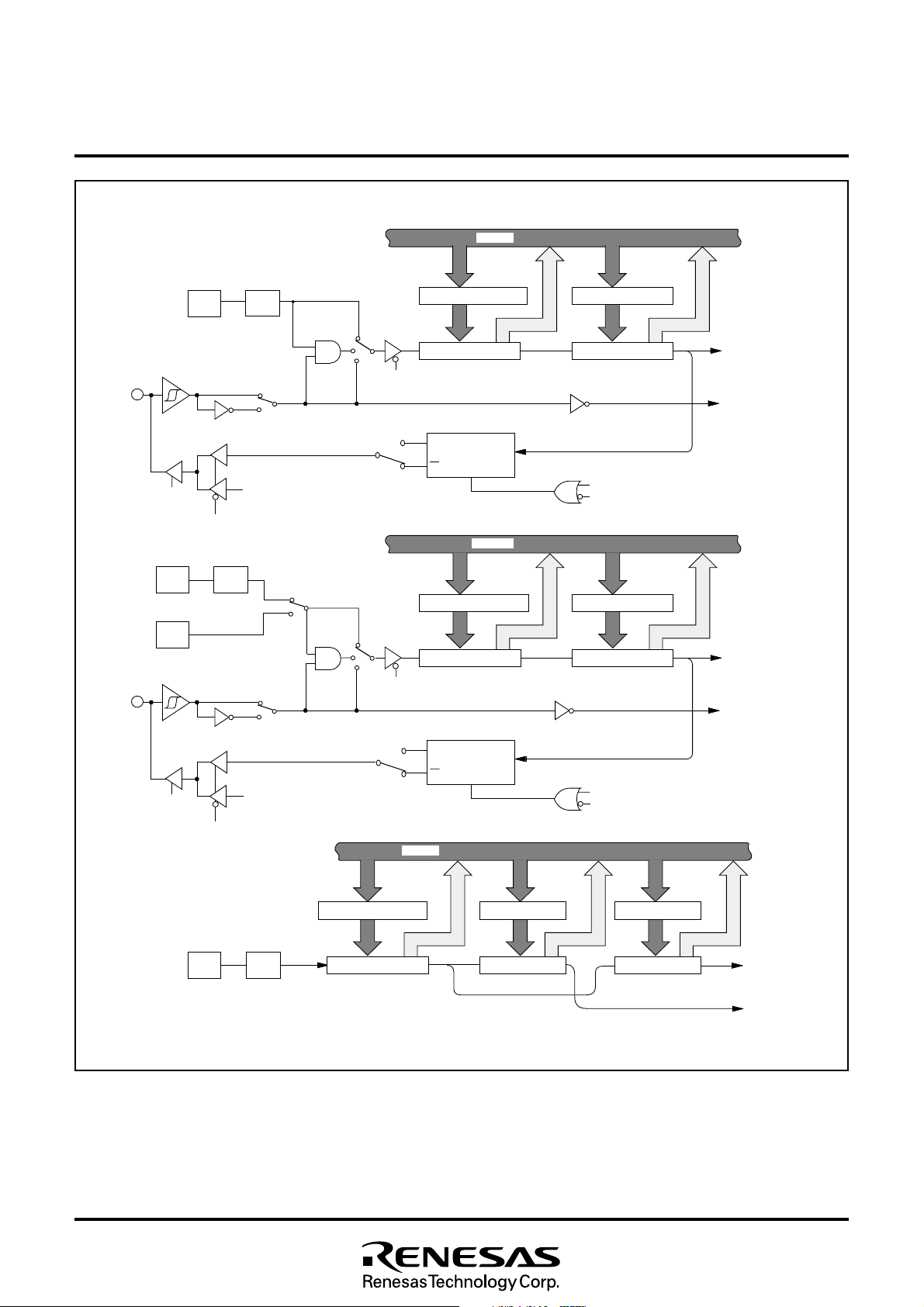
Fig. 10 Port block diagram (1)
15
Page 17
MITSUBISHI MICROCOMPUTERS
s
t
t
t
s
t
t
s
t
t
t
s
s
t
s
s
s
t
t
t
3885 Group
SINGLE-CHIP 8-BIT CMOS MICROCOMPUTER
( 9 ) P o r t P 44
P 4 o u t p u t s t r u c t u r e s e l e c t i o n b i t
S e r i a l I / O e n a b l e b i
R e c e i v e e n a b l e b i
D a t a b u
( 1 1 ) P o r t P 46
Serial I/O mode selection bi
S e r i a l I / O
s y n c h r o n o u s c l o c k s e l e c t i o n b i t
Serial I/O enable bi
Serial I/O enable bit
Data bu
Serial I/O clock output
D i r e c t i o n
r e g i s t e r
P o r t l a t c h
✻1
S e r i a l I / O i n p u t
P 4 o u t p u t s t r u c t u r e s e l e c t i o n b i
Direction
register
P o r t l a t c h
✻1
Serial I/O external clock input
(10) Port P45
5/
TXD P - c h a n n e l o u t p u t d i s a b l e b i
P 4
D a t a b u
S e r i a l I / O e n a b l e b i
T r a n s m i t e n a b l e b i
(12) Port P47
Serial I/O mode selection bi
Serial I/O enable bi
SRDY
Data bu
Serial I/O ready output
Direction
register
P o r t l a t c h
✻1
S e r i a l I / O o u t p u t
Serialized IRQ enable bit
output enable bi
Direction
register
P o r t l a t c h
CLKRUN output
(13) Ports P50 to P53
P 5 i o p e n d r a i n s e l e c t i o n b i t
D i r e c t i o n
r e g i s t e r
Data bu
Port latch
I n t e r r u p t i n p u t
(15) Ports P56, P57
P W M0 ( P W M1) o u t p u t p i n s e l e c t i o n b i t
i s s w i t c h e d t o p o r t P 4 p i n i n p u t l e v e l b y t h e P 8 f u n c t i o n s e l e c t i o n b i t o f t h e p o r t c o n t r o
✻1 . R e a d i n g t h e p o r t P 8 r e g i s t e r ( a d d r e s s 0 0 1 01
P W
P W M
0 (
M1) e n a b l e b i t
Data bu
P W
o u t p u
P W M
0 1 (
r e g i s t e r 2 ( P C T L 2 ) .
D i r e c t i o n
r e g i s t e r
P o r t l a t c h
M1
1)
t
D - A c o n v e r t e r o u t p u
D-A1 (D-A2) output enable bit
6)
(14) Ports P54, P55
Direction
register
Data bu
Port latch
Pulse output mode
Timer output
(16) Port P6
Data bu
C N T
C N T R
D i r e c t i o n
r e g i s t e r
P o r t l a t c h
0,
R1 i n t e r r u p t i n p u t
A-D converter input
A n a l o g i n p u t p i n s e l e c t i o n b i t
l
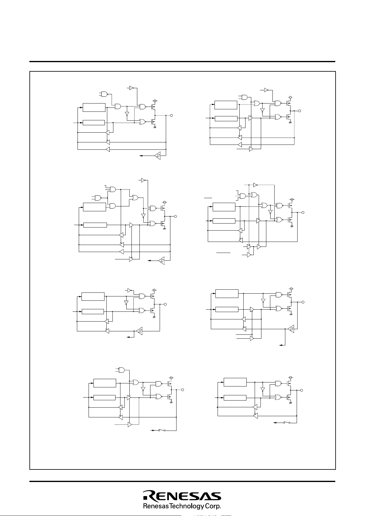
Fig. 11 Port block diagram (2)
16
Page 18
MITSUBISHI MICROCOMPUTERS
s
g
t
e
t
e
t
s
s
3885 Group
SINGLE-CHIP 8-BIT CMOS MICROCOMPUTER
( 1 7 ) P o r t s P 70 t o P 7
D i r e c t i o n
r e g i s t e r
D a t a b u
( 1 9 ) P o r t P 7
D a t a b u s
P o r t l a t c h
6
I2C - B U S i n t e r f a c
e n a b l e b i
i s t e
D i r e c t i o n
r e
Port latch
S
DA
( 2 1 ) P o r t s P 80 t o P 8
LPC enable bit
Direction
register
2
r
output
3
(18) Ports P73 to P7
Data bu
✻2
(20) Port P7
I2C-BUS interfac
D a t a b u
D A
S
i n p u
✻3
(22) Ports P84 to P8
LPC enable bit
7
enable bi
Direction
register
5
D i r e c t i o n
r e g i s t e r
P o r t l a t c h
D i r e c t i o n
r e g i s t e r
Port latch
S
C L
o u t p u t
6
✻2
I n t e r r u p t i n p u t
CL
input
S
✻3
Data bus
( 2 3 ) P o r t P 8
D a t a b u s
✻2. T h e i n p u t l e v e l c a n b e s w i t c h e d b e t w e e n C M O S c o m p a t i b l e i n p u t l e v e l a n d T T L l e v e l b y t h e P 7 i n p u t l e v e l s e l e c t i o n b i t o f t h e p o r t
c o n t r o l r e g i s t e r 2 ( P C T L 2 ) .
R e a d i n g t h e p o r t P 8 d i r e c t i o n r e g i s t e r i s s w i t c h e d t o p o r t P 7 p i n i n p u t l e v e l b y t h e P 8 f u n c t i o n s e l e c t i o n b i t o f t h e p o r t c o n t r o l r e g i s t e r 2
( P C T L 2 ) .
✻3. T h e i n p u t l e v e l c a n b e s w i t c h e d b e t w e e n C M O S c o m p a t i b l e i n p u t l e v e l a n d S M B U S l e v e l b y t h e I2C - B U S i n t e r f a c e p i n i n p u t s e l e c t i o n
b i t o f t h e I
Port latch
7
S I R Q e n a b l e b i t
D i r e c t i o n
r e g i s t e r
Port latch
2
C c o n t r o l r e g i s t e r ( S I D ) .
L A D [ 3 : 0 ]
I R Q S E R
Data bus
Port latch
L R E S E T
L C L K
L F R A M E
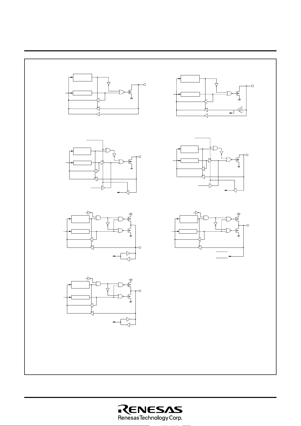
Fig. 12 Port block diagram (3)
17
Page 19
MITSUBISHI MICROCOMPUTERS
3885 Group
SINGLE-CHIP 8-BIT CMOS MICROCOMPUTER
b 7b
0
Port control register 1
1 6
( P C T L 1 : a d d r e s s 0 0 2 E
)
P00–P03 output structure selection bit
0: CMOS
1: N-channel open-drain
P0
4
–P07 output structure selection bit
0: CMOS
1: N-channel open-drain
P1
0
–P13 output structure selection bit
0: CMOS
1: N-channel open-drain
P1
4
–P17 output structure selection bit
0: CMOS
1: N-channel open-drain
P3
0
–P33 pull-up control bit
0: No pull-up
1: Pull-up
P3
4
–P37 pull-up control bit
0: No pull-up
1: Pull-up
PWM
0
enable bit
0: PWM
0
output disabled
1: PWM
0
output enabled
PWM
1
enable bit
0: PWM
1
output disabled
1: PWM
1
output enabled
b7 b0
Port control register 2
( P C T L 2 : a d d r e s s 0 0 2 F
1 6
)
N o t u s e d ( r e t u r n s “ 0 ” w h e n r e a d )
P 7 i n p u t l e v e l s e l e c t i o n b i t ( P 7
0
- P 75)
0 : C M O S i n p u t l e v e l
1 : T T L i n p u t l e v e l
P 4 o u t p u t s t r u c t u r e s e l e c t i o n b i t ( P 4
2
, P 43, P 44, P 46)
0 : C M O S
1 : N - c h a n n e l o p e n - d r a i n
P 8 f u n c t i o n s e l e c t i o n b i t
0 : P o r t P 8 / P o r t P 8 d i r e c t i o n r e g i s t e r
1 : P o r t P 4 i n p u t r e g i s t e r / P o r t P 7 i n p u t r e g i s t e r
I N T
2
, I N T3, I N T4 i n t e r r u p t s w i t c h b i t
0 : I N T
2 0
, I N T
3 0
, I N T
4 0
i n t e r r u p t
1 : I N T
2 1
, I N T
3 1
, I N T
4 1
i n t e r r u p t
T i m e r Y c o u n t s o u r c e s e l e c t i o n b i t
0 : f ( X
I N
) / 1 6 ( f ( X
C I N
) / 1 6 i n l o w - s p e e d m o d e )
1 : f ( X
C I N
)
O s c i l l a t i o n s t a b i l i z i n g t i m e s e t a f t e r S T P i n s t r u c t i o n r e l e a s e d b i t
0 : A u t o m a t i c s e t “ 0 1
1 6
” t o t i m e r 1 a n d “ F F
1 6
” t o p r e s c a l e r 1 2
1 : N o a u t o m a t i c s e t
C o m p a r a t o r r e f e r e n c e i n p u t s e l e c t i o n b i t
0 : P 2
0
/ C M P
R E F
i n p u t
1 : R e f e r e n c e i n p u t f i x e d
Fig. 13 Structure of port I/O related registers (1)
18
Page 20
MITSUBISHI MICROCOMPUTERS
SINGLE-CHIP 8-BIT CMOS MICROCOMPUTER
b 7b0
P o r t P 5 i n p u t r e g i s t e r
( P 5 I : a d d r e s s 0 F F 8
P 50 i n p u t l e v e l b i t
P 5
1
i n p u t l e v e l b i t
P 5
2
i n p u t l e v e l b i t
P 5
3
i n p u t l e v e l b i t
T h e s e b i t s d i r e c t l y s h o w t h e p i n i n p u t l e v e l s .
0 : “ L ” l e v e l i n p u t
1 : “ H ” l e v e l i n p u t
N o t u s e d ( r e t u r n s “ 0 ” w h e n r e a d )
b 7b0
P o r t c o n t r o l r e g i s t e r 3
( P C T L 3 : a d d r e s s 0 F F 9
1 6
)
1 6
)
3885 Group
Fig. 14 Structure of port I/O related registers (2)
P 50 o p e n d r a i n s e l e c t i o n b i t
P 5
1
o p e n d r a i n s e l e c t i o n b i t
P 5
2
o p e n d r a i n s e l e c t i o n b i t
P 5
3
o p e n d r a i n s e l e c t i o n b i t
0 : C M O S
1 : N - c h a n n e l o p e n d r a i n
N o t u s e d ( r e t u r n s “ 0 ” w h e n r e a d )
19
Page 21

MITSUBISHI MICROCOMPUTERS
3885 Group
SINGLE-CHIP 8-BIT CMOS MICROCOMPUTER
INTERRUPTS
Interrupts occur by 16 sources among 22 sources: thirteen external, nine internal, and one software.
Interrupt Control
Each interrupt is controlled by an interrupt request bit, an interrupt
enable bit, and the interrupt disable flag except for the software interrupt caused by the BRK instruction. An interrupt occurs when
both the corresponding interrupt request bit and interrupt enable
bit are “1” and the interrupt disable flag is “0”.
Interrupt enable bits can be set or cleared by software.
Interrupt request bits can be cleared by software, but cannot be
set by software.
The BRK instruction interrupt cannot be disabled with any flag or
bit. The I (interrupt disable) flag disables all interrupts except the
BRK instruction interrupt.
When several interrupts occur at the same time, the interrupts are
serviced according to the priority.
Interrupt Operation
By acceptance of an interrupt, the following operations are automatically performed:
1. The contents of the program counter and the processor status
register are automatically pushed onto the stack.
2. The interrupt disable flag is set and the corresponding interrupt
request bit is cleared.
3. The interrupt jump destination address is read from the vector
table and stored into the program counter.
Interrupt Source Selection
Any of the following interrupt sources can be selected by the interrupt source selection register (INTSEL).
1. INT0 or Input buffer full
2. INT1 or Output buffer empty
3. Serial I/O receive or LRESET
4. Serial I/O transmission or SCLSDA
5. Timer 2 or INT5
6. CNTR0 or INT0
7. CNTR1 or INT1
8. A-D conversion or Key-on wake-up
External Interrupt Pin Selection
The external interrupt sources of INT2, INT3, and INT4 can be selected from either input pin from INT20, INT30, INT40 or input pin
from INT21, INT31, INT41 by the INT2, INT3, INT4 interrupt switch
bit (bit 4 of PCTL2).
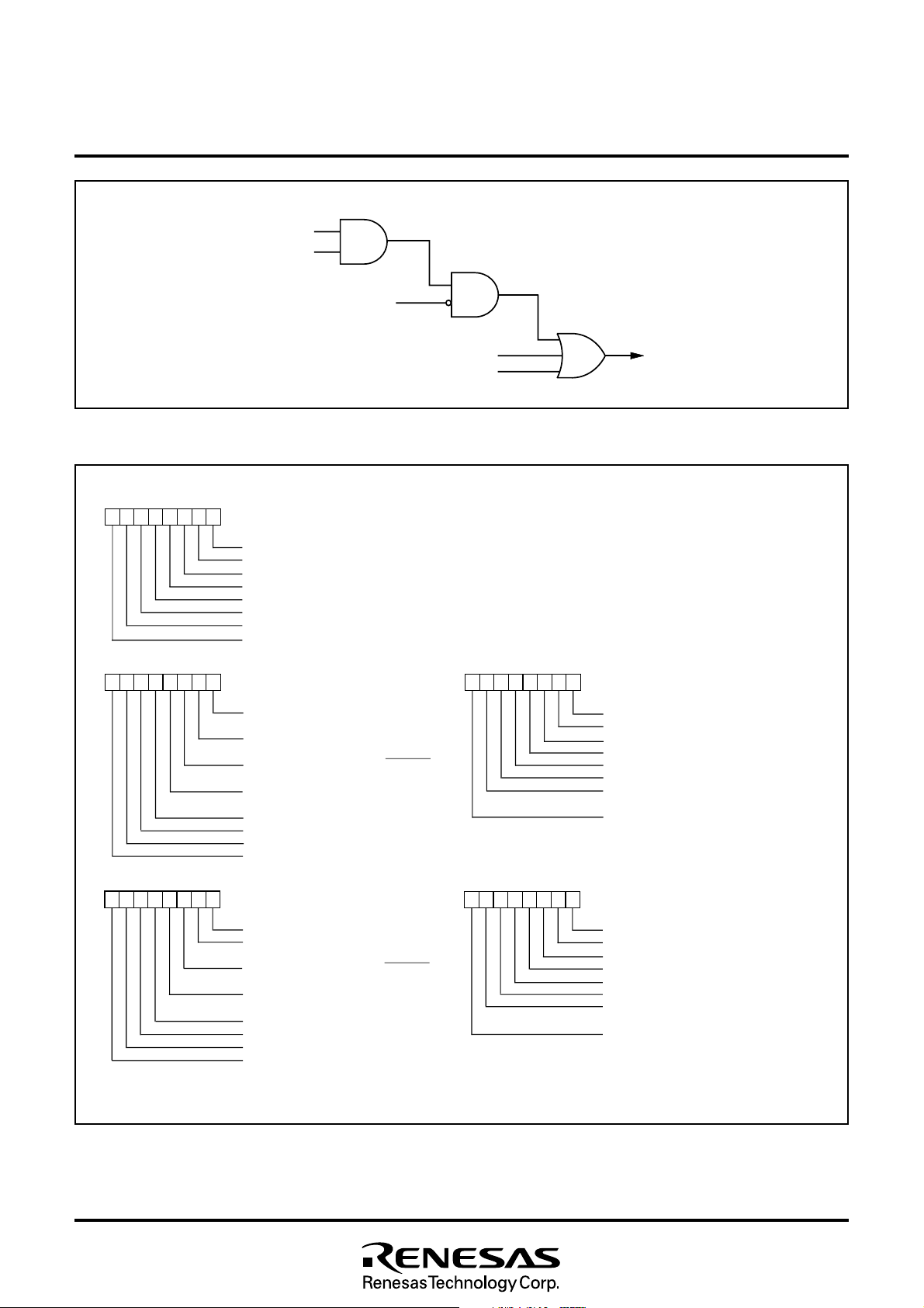
■ Notes
When setting the followings, the interrupt request bit may be set to
“1”.
•When setting external interrupt active edge
Related register: Interrupt edge selection register (address
003A16); Timer XY mode register (address
002316)
•When switching interrupt sources of an interrupt vector address
where two or more interrupt sources are allocated
Related register: Interrupt source selection register (address
003916)
•When setting input pin of external interrupts INT2, INT3 and INT4
Related register: INT2, INT3, INT4 interrupt switch bit of Port con-
trol register 2 (bit 4 of address 002F16)
When not requiring the interrupt occurrence synchronized with
these setting, take the following sequence.
➀ Set the corresponding interrupt enable bit to “0” (disabled).
➁ Set the active edge selection bit or the interrupt source selec-
tion bit to “1”.
➂ Set the corresponding interrupt request bit to “0” after 1 or more
instructions have been executed.
➃ Set the corresponding interrupt enable bit to “1” (enabled).
20
Page 22
Table 8 Interrupt vector addresses and priority
Interrupt Source
Reset (Note 2)
INT0
Input buffer full
(IBF)
INT1
Output buffer
empty (OBE)
Priority
1
2
3
Vector Addresses (Note 1)
High
16
FFFD
FFFB16
FFF916
Low
FFFC16
FFFA16
FFF816
MITSUBISHI MICROCOMPUTERS
SINGLE-CHIP 8-BIT CMOS MICROCOMPUTER
Interrupt Request
Generating Conditions
At reset
At detection of either rising or
falling edge of INT0 input
At input data bus buffer writing
At detection of either rising or
falling edge of INT1 input
At output data bus buffer reading
3885 Group
Remarks
Non-maskable
External interrupt
(active edge selectable)
External interrupt
(active edge selectable)
Serial I/O
reception
LRESET At falling edge of LRESET input External interrupt
Serial I/O
transmission
SCL, SDA
Timer X
Timer Y
Timer 1
Timer 2
INT5
CNTR0
INT0
CNTR1
INT1
I2C
INT2
INT3
INT4
10
11
12
13
14
15
4
5
6
7
8
9
FFF716
FFF516
FFF316
FFF116
FFEF16
FFED16
FFEB16
FFE916
FFE716
FFE516
FFE316
FFE116
FFF616
FFF416
FFF216
FFF016
FFEE16
FFEC16
FFEA16
FFE816
FFE616
FFE416
FFE216
FFE016
At completion of serial I/O data
reception
At completion of serial I/
Otransfer shift or when transmission buffer is empty
At detection of either rising or
falling edge of SCL or SDA
At timer X underflow
At timer Y underflow
At timer 1 underflow
At timer 2 underflow
At detection of either rising or
falling edge of INT5 input
At detection of either rising or
falling edge of CNTR0 input
At detection of either rising or
falling edge of INT0 input
At detection of either rising or
falling edge of CNTR1 input
At detection of either rising or
falling edge of INT1 input
At completion of data transfer
At detection of either rising or
falling edge of INT2 input
At detection of either rising or
falling edge of INT3 input
At detection of either rising or
falling edge of INT4 input
Valid when serial I/O is selected
Valid when serial I/O is selected
External interrupt
(active edge selectable)
STP release timer underflow
External interrupt
(active edge selectable)
External interrupt
(active edge selectable)
External interrupt
(active edge selectable)
External interrupt
(active edge selectable)
External interrupt (falling valid)
External interrupt
(active edge selectable)
External interrupt
(active edge selectable)
External interrupt
(active edge selectable)
A-D converter
16
Key-on wake-up
BRK instruction
Notes 1: Vector addresses contain interrupt jump destination addresses.
2: Reset functions in the same way as an interrupt with the highest priority.
17
FFDF16
FFDD16
FFDE16
FFDC16
At completion of A-D conversion
At falling of port P3 (at input) input logical level AND
At BRK instruction execution
External interrupt (falling valid)
Non-maskable software interrupt
21
Page 23
Interrupt request bi
t
t
I n t e r r u p t e n a b l e b i t
I n t e r r u p t d i s a b l e f l a g ( I )
MITSUBISHI MICROCOMPUTERS
3885 Group
SINGLE-CHIP 8-BIT CMOS MICROCOMPUTER
Fig. 15 Interrupt control
b7
b7
b7
b0
b0
b0
BRK instruction
Interrupt edge selection register
(INTEDGE : address 003A
INT0 active edge selection bit
INT
1
active edge selection bit
Not used (returns “0” when read)
INT
2
active edge selection bit
INT
3
active edge selection bit
INT
4
active edge selection bit
INT
5
active edge selection bit
Not used (returns “0” when read)
Interrupt request register 1
(IREQ1 : address 003C
INT0/input buffer full interrupt request
bit
INT
1
/output buffer empty interrupt
request bit
Serial I/O receive interrupt/LRESET
request bit
Serial I/O transmit/S
request bit
Timer X interrupt request bit
Timer Y interrupt request bit
Timer 1 interrupt request bit
Timer 2/INT
5
interrupt request bit
Interrupt control register 1
(ICON1 : address 003E
INT0/input buffer full interrupt enable bit
INT
1
/output buffer empty interrupt enable
bit
Serial I/O receive interrupt/LRESET
enable bit
Serial I/O transmit/S
enable bit
Timer X interrupt enable bit
Timer Y interrupt enable bit
Timer 1 interrupt enable bit
Timer 2/INT
5
interrupt enable bit
16
)
16
)
CL
, SDA interrupt
16
)
CL
, S
DA
interrupt
Rese
0 : Falling edge active
1 : Rising edge active
b7
b7
0
Interrupt request
b0
Interrupt request register 2
(IREQ2 : address 003D
CNTR0/INT0 interrupt request bit
CNTR
1
/INT1 interrupt request bit
2
I
C interrupt request bit
INT
2
interrupt request bit
INT
3
interrupt request bit
INT
4
interrupt request bit
AD converter/key-on wake-up interrupt
request bit
Not used (returns “0” when read)
0 : No interrupt request issued
1 : Interrupt request issued
b0
Interrupt control register 2
(ICON2 : address 003F
CNTR0/INT0 interrupt enable bit
CNTR
1
/INT1 interrupt enable bit
2
I
C interrupt enable bit
INT
2
interrupt enable bit
INT
3
interrupt enable bit
INT
4
interrupt enable bit
AD converter/key-on wake-up interrupt
enable bit
Not used (returns “0” when read)
(Do not write “1” to this bit)
0 : Interrupts disabled
1 : Interrupts enabled
16
)
16
)
Fig. 16 Structure of interrupt-related registers (1)
22
Page 24
MITSUBISHI MICROCOMPUTERS
3885 Group
SINGLE-CHIP 8-BIT CMOS MICROCOMPUTER
b 7
b 0
I n t e r r u p t s o u r c e s e l e c t i o n r e g i s t e r
( I N T S E L : a d d r e s s 0 0 3 9
1 6
)
INT0/input buffer full interrupt source selection bit
0 : INT
0
interrupt
1 : Input buffer full interrupt
INT
1
/output buffer empty interrupt source selection bit
0 : INT
1
interrupt
1 : Output buffer empty interrupt
Serial I/O receive/LRESET interrupt source selection bit
0 : Serial I/O receive
1 : LRESET interrupt
Serial I/O transmit/S
CL
, SDA interrupt source selection bit
0 : Serial I/O transmit interrupt
1 : S
CL
, SDA interrupt
Timer 2/INT
5
interrupt source selection bit
0 : Timer 2 interrupt
1 : INT
CNTR
0 : CNTR
1 : INT
CNTR
0 : CNTR
1 : INT
5
interrupt
0
/INT0 interrupt source selection bit
0
interrupt
0
interrupt
1
/INT1 interrupt source selection bit
1
interrupt
1
interrupt
AD converter/key-on wake-up interrupt source selection bit
0 : A-D
converter interrupt
1 : Key-on wake-up interrupt
Fig. 17 Structure of interrupt-related registers (2)
23
Page 25
MITSUBISHI MICROCOMPUTERS
3885 Group
SINGLE-CHIP 8-BIT CMOS MICROCOMPUTER
Key Input Interrupt (Key-on Wake Up)
A Key input interrupt request is generated by applying “L” level to
any pin of port P3 that have been set to input mode. In other
words, it is generated when the logical AND of all port P3 input
P o r t P X x
“ L ” l e v e l o u t p u t
P o r t c o n t r o l r e g i s t e r 1
P 3
P 3
P 3
7
o u t p u t
6
o u t p u t
5
o u t p u t
✻
✻
✻
B i t 5 = “ 0 ”
✻✻
✻✻
✻✻
Port P3
direction register = “1”
P o r t P 3
7
l a t c h
Port P3
direction register = “1”
P o r t P 3
6
l a t c h
P o r t P 3
5
l a t c h
Port P3
direction register = “1”
goes from “1” to “0”. An example of using a key input interrupt is
shown in Figure 18, where an interrupt request is generated by
pressing one of the keys consisted as an active-low key matrix
which inputs to ports P30–P33.
7
6
5
K e y i n p u t i n t e r r u p t r e q u e s t
P 3
4
o u t p u t
P3
3
P3
P 3
1
0
P 3
input
2
input
i n p u t
i n p u t
✻
P o r t c o n t r o l r e g i s t e r 1
B i t 4 = “ 1 ”
✻
✻
✻
✻
✻✻
✻✻
✻✻
✻✻
✻✻
P o r t P 3
l a t c h
Port P3
latch
Port P3
latch
Port P3
latch
P o r t P 30
l a t c h
P o r t P 3
d i r e c t i o n r e g i s t e r = “ 1 ”
4
Port P3
direction register = “0”
3
P o r t P 3
d i r e c t i o n r e g i s t e r = “ 0 ”
2
P o r t P 3
d i r e c t i o n r e g i s t e r = “ 0 ”
1
P o r t P 3
d i r e c t i o n r e g i s t e r = “ 0 ”
4
3
Port P3 input circuit
Comparator circuit
2
1
0
✻ P-channel transistor for pull-up
✻✻ CMOS output buffer
Fig. 18 Connection example when using key input interrupt and port P3 block diagram
24
Page 26
MITSUBISHI MICROCOMPUTERS
3885 Group
SINGLE-CHIP 8-BIT CMOS MICROCOMPUTER
TIMERS
The 3885 group has four timers: timer X, timer Y, timer 1, and
timer 2.
The division ratio of each timer or prescaler is given by 1/(n + 1),
where n is the value in the corresponding timer or prescaler latch.
All timers are count down structure. When the timer reaches
“0016”, an underflow occurs at the next count pulse and the corresponding timer latch is reloaded into the timer and the count is
continued. When a timer underflows, the interrupt request bit corresponding to that timer is set to “1”.
b7
Fig. 19 Structure of timer XY mode register
b 0
Timer XY mode register
(TM : address 0023
T i m e r X o p e r a t i n g m o d e b i t
b 1 b 0
0 0 : T i m e r m o d e
0 1 : P u l s e o u t p u t m o d e
1 0 : E v e n t c o u n t e r m o d e
1 1 : P u l s e w i d t h m e a s u r e m e n t m o d e
C N T R
0
a c t i v e e d g e s e l e c t i o n b i t
0 : I n t e r r u p t a t f a l l i n g e d g e
C o u n t a t r i s i n g e d g e i n e v e n t
c o u n t e r m o d e
1 : I n t e r r u p t a t r i s i n g e d g e
C o u n t a t f a l l i n g e d g e i n e v e n t
c o u n t e r m o d e
T i m e r X c o u n t s t o p b i t
0 : C o u n t s t a r t
1 : C o u n t s t o p
Timer Y operating mode bit
b5b4
0 0 : Timer mode
0 1 : Pulse output mode
1 0 : Event counter mode
1 1 : Pulse width measureme nt mode
CNTR
1
active edge selection bit
0: Interrupt at falling edge
Count at rising edge in event
counter mode
1: Interrupt at rising edge
Count at falling edge in event
counter mode
Timer Y count stop bit
0: Count start
1: Count stop
16
)
Timer 1 and Timer 2
The count source of prescaler 12 is the oscillation frequency divided by 16. The output of prescaler 12 is counted by timer 1 and
timer 2, and a timer underflow sets the interrupt request bit.
Timer X and Timer Y
Timer X and Timer Y can each select one of four operating modes
by setting the timer XY mode register.
(1) Timer Mode
The timer counts f(XIN)/16.
(2) Pulse Output Mode
Timer X (or timer Y) counts f(XIN)/16. Whenever the contents of
the timer reach “0016”, the signal output from the CNTR0 (or
CNTR1) pin is inverted. If the CNTR0 (or CNTR1) active edge selection bit is “0”, output begins at “ H”.
If it is “1”, output starts at “L”. When using a timer in this mode, set
the corresponding port P54 ( or port P55) direction register to output mode.
(3) Event Counter Mode
Operation in event counter mode is the same as in timer mode,
except that the timer counts signals input through the CNTR0 or
CNTR1 pin.
When the CNTR0 (or CNTR1) active edge selection bit is “0”, the
rising edge of the CNTR0 (or CNTR1) pin is counted.
When the CNTR0 (or CNTR1) active edge selection bit is “1”, the
falling edge of the CNTR0 (or CNTR1) pin is counted.
(4) Pulse Width Measurement Mode
If the CNTR0 (or CNTR1) active edge selection bit is “0”, the timer
counts f(XIN)/16 while the CNTR0 (or CNTR1) pin is at “H”. If the
CNTR0 (or CNTR1) active edge selection bit is “1”, the timer
counts while the CNTR0 (or CNTR1) pin is at “L”.
The count can be stopped by setting “1” to the timer X (or timer Y)
count stop bit in any mode. The corresponding interrupt request
bit is set each time a timer overflows.
The count source for timer Y in the timer mode or the pulse output
mode can be selected from either f(XIN)/16 or f(XCIN) by the timer
Y count source selection bit of the port control register 2 (bit 5 of
PCTL2).
25
Page 27
s
D a t a b u
MITSUBISHI MICROCOMPUTERS
3885 Group
SINGLE-CHIP 8-BIT CMOS MICROCOMPUTER
( f ( X
4
/ C N T R
P 5
d i r e c t i o n r e g i s t e r
(f(X
CIN
) in low-speed mode)
P 55/ C N T R
direction register
O s c i l l a t o r
I N
C I N
) i n l o w - s p e e d m o d e )
0
4
P o r t P 5
Pulse output mode
O s c i l l a t o r
I N
)
O s c i l l a t o r
f ( X
C I N
)
1
Port P5
5
Pulse output mode
)
C N T R
e d g e s e l e c t i o n
b i t
Divider
1 / 1 6f ( X
CNTR
edge selection
bit
D i v i d e r
1 / 1 6f ( X
0
a c t i v e
“ 0 ”
“1”
P o r t P 5
4
l a t c h
T i m e r Y c o u n t s o u r c e
s e l e c t i o n b i t
“ 0 ”
“1”
1
active
“ 0 ”
“ 1 ”
P o r t P 5 5
l a t c h
P u l s e w i d t h
m e a s u r e m e n t
m o d e
E v e n t
c o u n t e r
m o d e
C N T R
e d g e s e l e c t i o n
b i t
Pulse width
measurement mode
Event
counter
mode
C N T R
e d g e s e l e c t i o n
b i t
Timer mode
Pulse output mode
T i m e r X c o u n t s t o p b i t
0
a c t i v e
“ 1 ”
“ 0 ”
Timer mode
Pulse output mode
Timer Y count stop bit
1
a c t i v e
“1”
“0”
Data bus
P r e s c a l e r X l a t c h ( 8 )
Prescaler X (8)
Q
T o g g l e f l i p - f l o p
Q
R
Data bus
Prescaler Y latch (8)
Prescaler Y (8)
Q
Toggle flip-flop
Q
R
T i m e r X l a t c h ( 8 )
T i m e r X ( 8 )
T o t i m e r X i n t e r r u p t
r e q u e s t b i t
T o C N T R
0
i n t e r r u p t
r e q u e s t b i t
T
Timer X latch write pulse
Pulse output mode
T i m e r Y l a t c h ( 8 )
Timer Y (8)
To timer Y interrupt
request bit
To CNTR
1
interrupt
request bit
T
T i m e r Y l a t c h w r i t e p u l s e
P u l s e o u t p u t m o d e
Prescaler 12 latch (8)
D i v i d e rO s c i l l a t o r
Prescaler 12 (8)
(f(X
CIN
) in low-speed mode)
1/16f(XIN)
Fig. 20 Block diagram of timer X, timer Y, timer 1, and timer 2
26
Timer 1 latch (8)
Timer 1 (8)
Timer 2 latch (8)
T i m e r 2 ( 8 )
To timer 2 interrupt
request bit
T o t i m e r 1 i n t e r r u p t
r e q u e s t b i t
Page 28
WATCHDOG TIMER
The watchdog timer gives a mean of returning to the reset status
when a program cannot run on a normal loop (for example, because of a software run-away). The watchdog timer consists of an
8-bit watchdog timer L and an 8-bit watchdog timer H.
Basic Operation of Watchdog Timer
When any data is not written into the watchdog timer control register (WDTCON) after resetting, the watchdog timer is in the stop
state. The watchdog timer starts to count down by writing an optional value into the watchdog timer control register (WDTCON) and
an internal reset occurs at an underflow of the watchdog timer H.
Accordingly, programming is usually performed so that writing to
the watchdog timer control register (WDTCON) may be started before an underflow. When the watchdog timer control register
(WDTCON) is read, the values of the high-order 6 bits of the
watchdog timer H, STP instruction disable bit, and watchdog timer
H count source selection bit are read.
Initial Value of Watchdog Timer
At reset or writing to the watchdog timer control register
(WDTCON), each watchdog timer H and L is set to “FF16”.
MITSUBISHI MICROCOMPUTERS
3885 Group
SINGLE-CHIP 8-BIT CMOS MICROCOMPUTER
●Watchdog timer H count source selection bit operation
Bit 7 of WDTCON permits selecting a watchdog timer H count
source. When this bit is set to “0”, the count source becomes the
underflow signal of watchdog timer L. The detection time is set to
131.072 ms at f(XIN)=8 MHz and 32.768 s at f(XCIN)=32 kHz .
When this bit is set to “1”, the count source becomes the signal
divided by 16 for f(XIN) (or f(XCIN) in low speed mode). The detection time in this case is set to 512 µs at f(XIN)=8 MHz and 128 ms
at f(XCIN)=32 kHz . This bit is cleared to “0” after resetting.
●STP instruction disable bit
Bit 6 of WDTCON permits disabling the STP instruction when the
watchdog timer is in operation.
When this bit is “0”, the STP instruction is enabled.
When this bit is “1”, the STP instruction is disabled.
When this bit is “1”, the STP instruction execution cause an internal reset. When this bit is set to “1”, it cannot be rewritten to “0” by
program. This bit is cleared to “0” after resetting.
16” is set when
“FF
XCIN
Main clock division
ratio selection bits
(Note)
XIN
STP instruction disable bit
RESET
Note: Either high-speed, middle-speed or low-speed mode is selected by bits 7 and 6 of the CPU mode register.
watchdog timer
control register is
written to.
“10”
1/16
“00”
“01”
STP instruction
Fig. 21 Block diagram of Watchdog timer
b 7
Watchdog timer L (8)
“0”
“1”
Watchdog timer H count
source selection bit
b0
Watchdog timer H (8)
Watchdog timer control register
(WDTCON : address 001E
Watchdog timer H (for read-out of high-order 6 bit)
STP instruction disable bit
0: STP instruction enabled
1: STP instruction dis abled
Reset
circuit
Data bus
16” is set when
“FF
watchdog timer
control register is
written to.
Internal reset
16
)
Fig. 22 Structure of Watchdog timer control register
Watchdog timer H count source selection bit
0: Watchdog timer L underflow
1: f(X
IN
)/16 or f(X
CIN
)/16
27
Page 29
MITSUBISHI MICROCOMPUTERS
3885 Group
SINGLE-CHIP 8-BIT CMOS MICROCOMPUTER
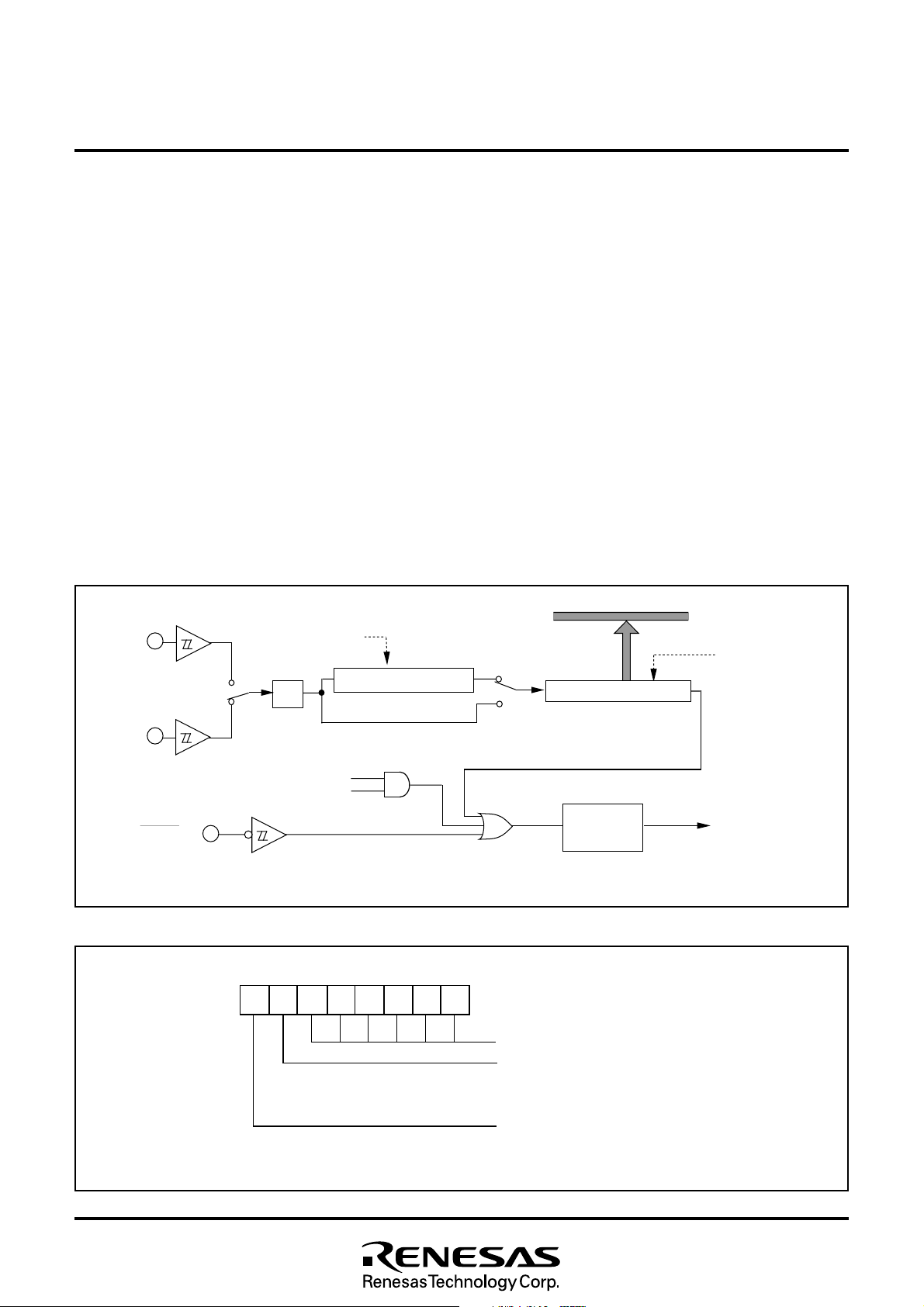
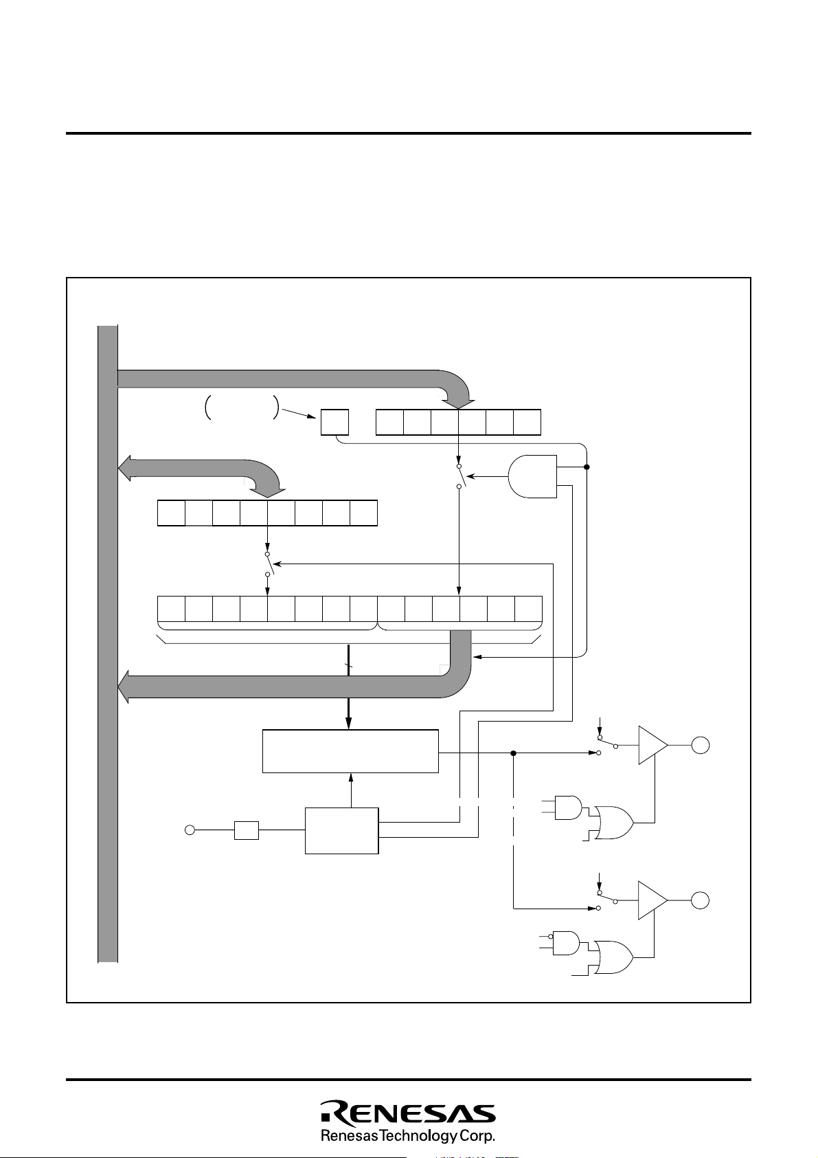
PULSE WIDTH MODULATION (PWM)
OUTPUT CIRCUIT
The 3885 group has two PWM output circuits, PWM0 and PWM1,
with 14-bit resolution respectively. These can operate independently. When the oscillation frequency X
Data Bus
Set to “1”
at write
bit 7
IN is 8 MHz, the minimum
bit 7
bit 5
bit 0
PWM0H register (Address 0030
resolution bit width is 250 ns and the cycle period is 4096 µs. The
PWM timing generator supplies a PWM control signal based on a
signal that is the frequency of the XIN clock.
The following explanation assumes f(XIN) = 8 MHz.
PWM0L register (Address 003116)
bit 0
16)
PWM0 latch (14 bits)
MSB
f(XIN)
(8MHz)
(4MHz)
1/2
14
14-bit PWM0 circuit
PWM0
(64 µs period)
timing
generator
(4096 µs period)
LSB
PWM0
PWM0 output selection bit
PWM0 enable bit
P30 direction register
PWM0 output selection bit
PWM
0 enable bit
P56 direction register
P3
0 latch
PWM0 enable bit
P5
6 latch
PWM
0 enable bit
0/PWM00
P3
6/DA1/PWM01
P5
Fig. 23 PWM block diagram (PWM0)
28
Page 30
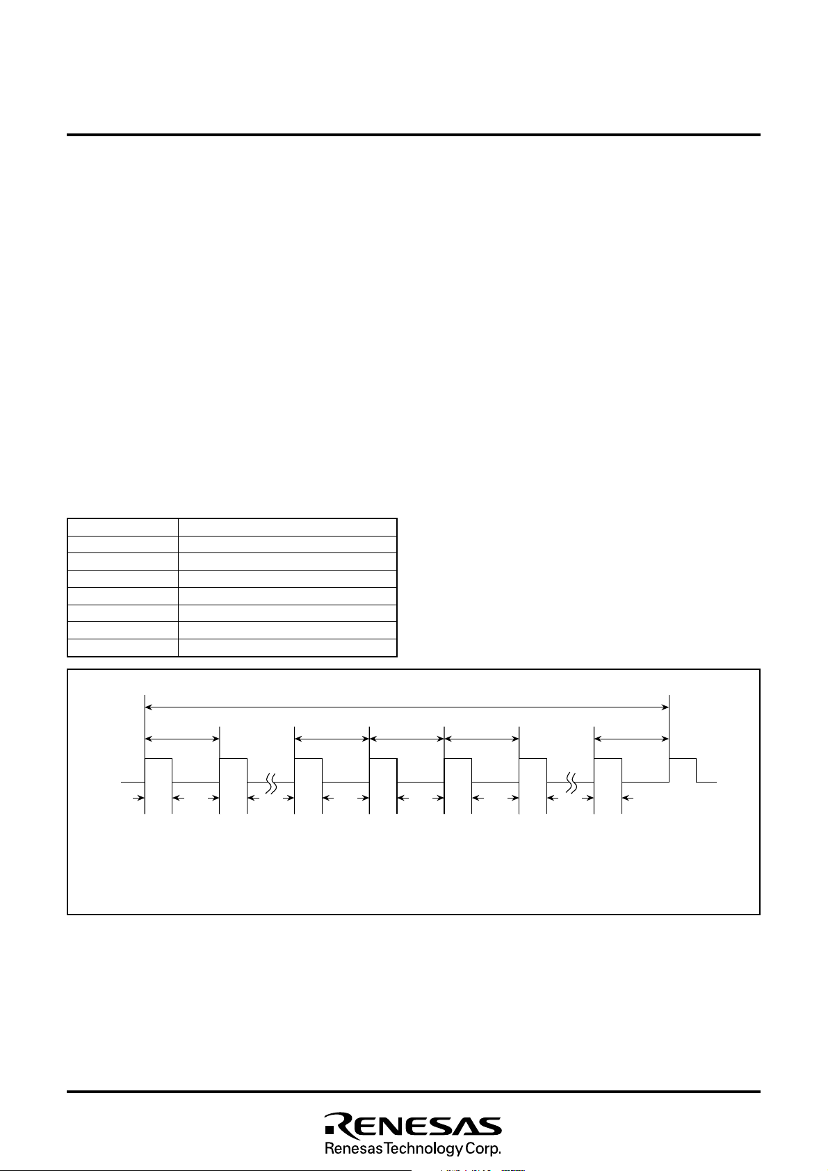
MITSUBISHI MICROCOMPUTERS
3885 Group
SINGLE-CHIP 8-BIT CMOS MICROCOMPUTER
Data Setup (PWM0)
The PWM0 output pin also functions as port P30 or P56. The
PWM0 output pin is selected from either P30/PWM00 or
P56/PWM01 by PWM0 output pin selection bit (bit 4 of ADCON).
The PWM0 output becomes enabled state by setting PWM
able bit (bit 6 of PCTL1). The high-order eight bits of output data
are set in the PWM0H register and the low-order six bits are set in
the PWM0L register.
PWM1 is set as the same way.
0 en-
PWM Operation
The 14-bit PWM data is divided into the low-order six bits and the
high-order eight bits in the PWM latch.
The high-order eight bits of data determine how long an “H”-level
signal is output during each sub-period. There are 64 sub-periods
in each period, and each sub-period is 256 ✕ τ (64 µs) long. The
signal is “H” for a length equal to N times τ, where τ is the minimum resolution (250 ns).
“H” or “L” of the bit in the ADD part shown in Figure 24 is added to
Table 9 Relationship between low-order 6 bits of data and
period set by the ADD bit
Low-order 6 bits of data (PWML)
000000
000001
000010
000100
001000
010000
100000
Sub-periods tm Lengthened (m=0 to 63)
LSB
None
m=32
m=16, 48
m=8, 24, 40, 56
m=4, 12, 20, 28, 36, 44, 52, 60
m=2, 6, 10, 14, 18, 22, 26, 30, 34, 38, 42, 46, 50, 54, 58, 62
m=1, 3, 5, 7, ................................................ ,57, 59, 61, 63
this “H” duration by the contents of the low-order 6-bit data according to the rule in Table 9.
That is, only in the sub-period tm shown by Table 9 in the PWM
cycle period T = 64t, its “H” duration is lengthened to the minimum
resolution τ added to the length of other periods.
For example, if the high-order eight bits of the 14-bit data are 0316
and the low-order six bits are 0516, the length of the “H”-level output in sub-periods t8, t24, t32, t40, and t56 is 4 τ, and its length is 3
τ in all other sub-periods.
Time at the “H” level of each sub-period almost becomes equal,
because the time becomes length set in the high-order 8 bits or
becomes the value plus τ, and this sub-period t (= 64 µs, approximate 15.6 kHz) becomes cycle period approximately.
Transfer From Register to Latch
Data written to the PWML register is transferred to the PWM latch
at each PWM period (every 4096 µs), and data written to the
PWMH register is transferred to the PWM latch at each sub-period
(every 64 µs). The signal which is output to the PWM output pin is
corresponding to the contents of this latch. When the PWML register is read, the latch contents are read. However, bit 7 of the
PWML register indicates whether the transfer to the PWM latch is
completed; the transfer is completed when bit 7 is “0” and it is not
done when bit 7 is “1”.
15.75 µs 15.75 µs 15.75 µs 16.0 µs 15.75 µs
Pulse width modulation register H
Pulse width modulation register L
Sub-periods where “H” pulse width is 16.0 µs :
Sub-periods where “H” pulse width is 15.75 µs :
Fig. 24 PWM timing
64 µs
m=0
64 µs
m=7
: 00111111
: 000101
4096 µs
64 µs
m=8
64 µs
m=9
15.75 µs
m = 8, 24, 32, 40, 56
m = all other values
64 µs
m=63
15.75 µs
29
Page 31

MITSUBISHI MICROCOMPUTERS
3885 Group
SINGLE-CHIP 8-BIT CMOS MICROCOMPUTER
PWM0H
register
PWM0L
register
P W M 0 l a t c h
( 1 4 b i t s )
E x a m p l e 1
PWM0 output
l o w - o r d e r
6 - b i t o u t p u t :
H L
1 6
, 2 4
6 A
Example 2
PWM0 output
l o w - o r d e r
6 - b i t o u t p u t :
H L
16
, 18
16
6A
Data 6A16 stored at address 0030
6A
5 9
1 6
16
Data 2416 stored at address 0031
1 3
1 6
1 6 5 3
1 6
1 A 9 3
A4
16
1 6
16
16
Bit 7 cleared after transfer
2 4
1 6
T r a n s f e r f r o m r e g i s t e r t o l a t c h
1 A A 4
1 6
T = 4096 µs
( 6 4 ✕ 6 4 µs )
Data 7B16 stored at address 0030
B 5
1 6
1AA4
16
1 E E 4
1 6
W h e n b i t 7 o f P W M 0 L i s 0 , t r a n s f e r
f r o m r e g i s t e r t o l a t c h i s d i s a b l e d .
7 B
1 6
Data 3516 stored at address 0031
35
16
T r a n s f e r f r o m r e g i s t e r t o l a t c h
1 E F 5
t = 64 µs
6 A6 A6
A6
A6A6
B6
B6
B6 A6
B6 B6B6
A6
B6B 6B6
A6
A6
A6
A6
B6
1
2
5 5 5 5
1 6
6B
16 ··············
( 1 0 7 ) ( 1 0 6 )
36 times 6A
5
5 5 5 5 5 5 5 5 5
16 ·············
28 times
106 ✕ 64 + 36
6 A 6 A 6 B 6B 6 B 6 A 6B 6B 6B 6 A 6 B 6B 6 B 6 A6 A 6 A 6 A 6 A 6 A 6A 6A 6 A 6 A 6 A 6 A 6 A 6 A
4 3 4 4 3 4 4 3 4
6A
16 ·······
6 B
1 6 · · · · · · · · · · · · · ·
2 4 t i m e s
40 times
1 0 6 ✕ 6 4 + 2 4
16
16
1 6
A6A6 B6 B6
B6
B
M i n i m u m r e s o l u t i o n b i t w i d t h τ = 0 . 2 5 µs
PWM output
2
8 - b i t
c o u n t e r
T h e A D D
p o r t i o n s w i t h
a d d i t i o n a l τ a r e
d e t e r m i n e d b y
P W M L .
6B 6A 69 68 67 02 01 6A 69 68 67 02 01
A D D A D D
0 2 0 1 0 0 F F FE F D 97 9 6 95 02 0 1 00F C FF F E F D 9 7 96 9 5FC
Fig. 25 14-bit PWM timing (PWM0)
t = 6 4 µs
·······
· · · · · · ·
H duration length specified by PWM0H
256 τ (64 µs), fixed
(256 ✕ 0.25 µs)
·······
· · · · · · ·
· · · · · · ·
· · · · · · ·
30
Page 32

MITSUBISHI MICROCOMPUTERS
3885 Group
SINGLE-CHIP 8-BIT CMOS MICROCOMPUTER
SERIAL I/O
Serial I/O
Serial I/O works as either clock synchronous serial I/O mode or
universal asynchronous receiver transmitter (UART) serial I/O
mode. A dedicated timer is also provided for baud rate generation.
Data bus
Receive buffer register
Receive shift register
Address 001C
Falling-edge detector
Transmit shift register
Transmit buffer register
Data bus
(f(X
mode)
CIN
) in low-speed
7/SRDY
/CLKRUN
P4
P4
P44/RXD
P46/S
f(X
5/TX
D
CLK
BRG count source selection bit
IN
)
F/F
1/4
(1) Clock Synchronous Serial I/O Mode
Clock synchronous serial I/O mode can be selected by setting the
serial I/O mode selection bit of the serial I/O control register (bit 6
of SIOCON) to “1”.
For clock synchronous serial I/O, the transmitter and the receiver
must use the same clock. When an internal clock is used, the
transfer starts by writing to the TB.
Address 0018
Serial I/O synchronous
clock selection bit
16
Frequency division ratio 1/(n+1)
16
Shift clock
Baud rate generator
Shift clock
Address 0018
Serial I/O control register
Clock control circuit
Clock control circuit
16
Address 001A
Receive buffer full flag (RBF)
Receive interrupt request (RI)
1/4
Transmit shift completion flag (TSC)
Transmit interrupt source selection bit
Transmit interrupt request (TI)
Transmit buffer empty flag (TBE)
Serial I/O status register
16
Fig. 26 Block diagram of clock synchronous serial I/O
Transfer shift clock
(1/2 to 1/2048 of the internal
clock, or an external clock)
TxD pin
RxD pin
S
RDY
pin
D
0
D
D
0
D
Write pulse to transmit buffer
register (TB)
TBE = 0
TSC = 1
1: As the transmit interrupt (TI), which can be selected, either when the transmit buffer has emptied (TBE=1) or after the
Notes
transmit shift operation has ended (TSC=1), by setting the transmit interrupt source selection bit (TIC) of the serial I/O
TBE = 1
TSC = 0
control register.
2: If data is written to the transmit buffer register when TSC=0, the transmit clock is generated continuously and the next
serial data is output continuously from the TxD pin.
3: The receive interrupt (RI) is set when the receive buffer full flag (RBF) becomes “1” .
Fig. 27 Operation of clock synchronous serial I/O function
D
1
D
2
D
3
D
4
D
5
D
6
1
D
2
D
3
D
4
D
5
D
6
7
D
7
RBF = 1
TSC = 1
Overrun error (OE)
detection
31
Page 33

MITSUBISHI MICROCOMPUTERS
3885 Group
SINGLE-CHIP 8-BIT CMOS MICROCOMPUTER
(2) Asynchronous Serial I/O (UART) Mode
Universal asynchronous transmitter receiver (UART) serial I/O
mode can be selected by clearing the serial I/O mode selection bit
of the serial I/O control register to “0”.
Eight serial data transfer formats can be selected, and the transfer
formats used by a transmitter and receiver must be identical.
Both the transmit and receive shift registers have a buffer, but the
Data bus
Address
0018
16
Receive buffer register
Receive shift register
PE FE
SP detector
Frequency division ratio 1/(n+1)
Baud rate generator
ST/SP/PA generator
Transmit shift register
Transmit buffer register
Data bus
(f(X
CIN
) in low-speed mode)
P4
P4
6/SCLK
P4
4/RX
f(XIN)
5/TX
ST detector
D
BRG count source selection bit
D
Character length selection bit
1/4
Character length selection bit
OE
7 bits
8 bits
Serial I/O synchronous clock selection bit
two buffers assigned the same address. Since the shift register
cannot be written to or read from directly, transmit data is written
to the transmit buffer register, and receive data is read from the receive buffer register.
The transmit buffer register can also hold the next data to be
transmitted, and the receive buffer register can hold a character
while the next character is being received.
Serial I/O control register
Receive buffer full flag (RBF)
Receive interrupt request (RI)
Clock control circuit
1/16
Transmit interrupt source selection bit
Address
16
001A
1/16
UART control register
Transmit shift completion flag (TSC)
Transmit interrupt request (TI)
Serial I/O status register
Transmit buffer empty flag (TBE)
Address 001B
Address 0019
16
16
Fig. 28 Block diagram of UART mode
32
Page 34

Transmit or receive clock
MITSUBISHI MICROCOMPUTERS
3885 Group
SINGLE-CHIP 8-BIT CMOS MICROCOMPUTER
Transmit buffer write
Serial output TXD pin
Receive buffer read
Serial input R
signal
TBE=0 TBE=0
TSC=0
TBE=1
ST
0
D
1
1 start bit
7 or 8 data bit
1 or 0 parity bit
signal
ST
X
D pin
Notes
1: Error flag detection occurs at the same time that the RBF flag becomes “1” (at 1st stop bit, during reception).
2: As the transmit interrupt (TI), when either the TBE or TSC flag becomes “1”, can be selected to occur depending on the setting of the transmit
interrupt source selection bit (TIC) of the serial I/O control register.
3: The receive interrupt (RI) is set when the RBF flag becomes “1”.
4: After data is written to the transmit buffer when TSC=1, 0.5 to 1.5 cycles of the data shift cycle is necessary until changing to TSC=0.
0
1 or 2 stop bit (s)
D
1
Fig. 29 Operation of UART mode function
[Serial I/O Control Register (SIOCON)] 001A16
The serial I/O control register consists of eight control bits for the
serial I/O function.
[UART Control Register (UARTCON)] 001B16
The UART control register consists of four control bits (bits 0 to 3)
which are valid in UART mode and set the data format of an data
transfer. The POFF bit (bit4) is always valid and define the output
structure of the P45/TXD pin.
[Serial I/O Status Register (SIOSTS)] 001916
The read-only serial I/O status register consists of seven flags
(bits 0 to 6) which indicate the operating status of the serial I/O
function and various errors.
Three of the flags (bits 4 to 6) are valid only in UART mode.
The receive buffer full flag (bit 1) is cleared to “0” when the receive
buffer register is read.
If there is an error, it is detected at the same time that data is
transferred from the receive shift register to the receive buffer register, and the receive buffer full flag is set. A write to the serial I/O
status register clears all the error flags OE, PE, FE, and SE (bit 3
to bit 6, respectively). Writing “0” to the serial I/O enable bit (SIOE,
bit 7 of SIDCON) also clears all the status flags, including the error flags.
Bits 0 to 6 of the serial I/O status register are initialized to “0” at reset, but if the transmit enable bit (TE, bit 4 of SIOCON) has been
set to “1”, the transmit shift completion flag (TSC, bit 2) and the
transmit buffer empty flag (TBE, bit 0) become “1”.
TBE=1
STD
SP
RBF=1
STD
SP D
D
0
D
1
✽
Generated at 2nd bit in 2-stop-bit mode
RBF=0
0
D
1
TSC=1
SP
RBF=1
SP
✽
[Transmit Buffer Register/Receive Buffer
Register (TB/RB)] 0018
The transmit buffer register and the receive buffer register are located at the same address. The transmit buffer is write-only and
the receive buffer is read-only. If a character length is 7 bits, the
MSB data stored in the receive buffer is “0”.
16
[Baud Rate Generator (BRG)] 001C16
The baud rate generator determines the baud rate for serial transfer.
The baud rate generator divides the frequency of the count source
by 1/(n + 1), where n is the value written to the baud rate generator.
■ Notes
When setting the transmit enable bit to “1”, the serial I/O transmit
interrupt request bit is automatically set to “1”. When not requiring
the interrupt occurrence synchronized with the transmission enabled, take the following sequence.
➀ Set the serial I/O transmit interrupt enable bit to “0” (disabled).
➁ Set the transmit enable bit to “1”.
➂ Set the serial I/O transmit interrupt request bit to “0” after 1 or
more instructions have been executed.
➃ Set the serial I/O transmit interrupt enable bit to “1” (enabled).
33
Page 35

MITSUBISHI MICROCOMPUTERS
3885 Group
SINGLE-CHIP 8-BIT CMOS MICROCOMPUTER
b7
b7
b0
Serial I/O status register
(SIOSTS : address 001916)
Transmit buffer empty flag (TBE)
0: Buffer full
1: Buffer empty
Receive buffer full flag (RBF)
0: Buffer empty
1: Buffer full
Transmit shift completion flag (TSC)
0: Transmit shift in progress
1: Transmit shift completed
Overrun error flag (OE)
0: No error
1: Overrun error
Parity error flag (PE)
0: No error
1: Parity error
Framing error flag (FE)
0: No error
1: Framing error
Summing error flag (SE)
0: (OE) U (PE) U (FE)=0
1: (OE) U (PE) U (FE)=1
Not used (returns “1” when read)
b0
UART control register
(UARTCON : address 001B16)
Character length selection bit (CHAS)
0: 8 bits
1: 7 bits
Parity enable bit (PARE)
0: Parity checking disabled
1: Parity checking enabled
Parity selection bit (PARS)
0: Even parity
1: Odd parity
Stop bit length selection bit (STPS)
0: 1 stop bit
1: 2 stop bits
5/TXD P-channel output disable bit (POFF)
P4
0: CMOS output (in output mode)
1: N-channel open drain output (in output mode)
Not used (return “1” when read)
b7
b0
Serial I/O control register
(SIOCON : address 001A
BRG count source selection bit (CSS)
IN) (f(XCIN) in low-speed mode)
0: f(X
1: f(X
IN)/4 (f(XCIN)/4 in low-speed mode)
Serial I/O synchronous clock selection bit (SCS)
0: BRG output divided by 4 when clock synchronous
serial I/O is selected, BRG output divided by 16
when UART is selected.
1: External clock input when clock synchronous serial
I/O is selected, external clock input divided by 16
when UART is selected.
RDY output enable bit (SRDY)
S
0: P4
7 pin operates as ordinary I/O pin
7 pin operates as SRDY output pin
1: P4
Transmit interrupt source selection bit (TIC)
0: Interrupt when transmit buffer has emptied
1: Interrupt when transmit shift operation is completed
Transmit enable bit (TE)
0: Transmit disabled
1: Transmit enabled
Receive enable bit (RE)
0: Receive disabled
1: Receive enabled
Serial I/O mode selection bit (SIOM)
0: Clock asynchronous (UART) serial I/O
1: Clock synchronous serial I/O
Serial I/O enable bit (SIOE)
0: Serial I/O disabled
4 to P47 operate as ordinary I/O pins)
(pins P4
1: Serial I/O enabled
4 to P47 operate as serial I/O pins)
(pins P4
16)
Fig. 30 Structure of serial I/O control registers
34
Page 36

MULTI-MASTER I2C-BUS INTERFACE
The multi-master I2C-BUS interface is a serial communications circuit, conforming to the Philips I2C-BUS data transfer format. This
interface, offering both arbitration lost detection and a synchronous
functions, is useful for the multi-master serial communications.
Figure 31 shows a block diagram of the multi-master I2C-BUS interface and Table 10 lists the multi-master I2C-BUS interface
functions.
This multi-master I2C-BUS interface consists of the I2C address
register, the I2C data shift register, the I2C clock control register,
the I2C control register, the I2C status register, the I2C start/stop
condition control register and other control circuits.
When using the multi-master I2C-BUS interface, set 1 MHz or
more to system clock φ.
MITSUBISHI MICROCOMPUTERS
3885 Group
SINGLE-CHIP 8-BIT CMOS MICROCOMPUTER
2
Table 10 Multi-master I
Item
Format
Communication mode
SCL clock frequency
System clock φ = f(XIN)/2 (high-speed mode)
φ = f(XIN)/8 (middle-speed mode)
C-BUS interface functions
Function
In conformity with Philips I2C-BUS
standard:
10-bit addressing format
7-bit addressing format
High-speed clock mode
Standard clock mode
In conformity with Philips I2C-BUS
standard:
Master transmission
Master reception
Slave transmission
Slave reception
16.1 kHz to 400 kHz (at φ = 4 MHz)
Serial data
(SDA)
S2D
STSP
SEL
SIS
Serial
clock
(SCL)
Interrupt
generating
circuit
Noise
elimination
circuit
SIP
SSC4SSC3 SSC2SSC1 SSC0
I2C start/stop condition
control register
Noise
elimination
circuit
Interrupt request signal
CLSDA
IRQ)
(S
Clock
control
circuit
Data
control
circuit
AL
circuit
BB
circuit
S0D
b7 b0
I2C address register
SAD6 SAD5 SAD4 SAD3 SAD2 SAD1 SAD0 RWB
Address comparator
b7
I2C data shift register
S
0
b7 b0
FAST
ACK
ACK
S2
I2C clock control register
CCR4 CCR3 CCR2 CCR1 CCR0
MODE
BIT
Clock division
b0
Internal data bus
Stop selection
Interrupt
generating
circuit
Interrupt request signal
2
CIRQ)
(I
b7
MST TRX BB PIN
S1
AL AAS AD0 LRB
I2C status register
I2C clock control register
b7 b0
CLK
10BIT
TISS
STP
SAD
ALS
System clock (φ)
S1D
ES0
BC2 BC1 BC0
Bit counter
b0
Fig. 31 Block diagram of multi-master I2C-BUS interface
✽ : Purchase of MITSUBISHI ELECTRIC CORPORATIONS I2C components conveys a license under the Philips I2C Patent Rights to use these components
2
an I
C system, provided that the system conforms to the I2C Standard Specification as defined by Philips.
35
Page 37

[I2C Data Shift Register (S0)] 001216
The I2C data shift register (S0) is an 8-bit shift register to store receive data and write transmit data.
When transmit data is written into this register, it is transferred to
the outside from bit 7 in synchronization with the SCL clock, and
each time one-bit data is output, the data of this register are
shifted by one bit to the left. When data is received, it is input to
this register from bit 0 in synchronization with the SCL clock, and
each time one-bit data is input, the data of this register are shifted
by one bit to the left. The minimum 2 cycles of φ are required from
the rising of the SCL clock until input to this register.
The I2C data shift register is in a write enable status only when the
I2C-BUS interface enable bit (ES0 bit : bit 3 S1D) of the I2C control register is “1”. The bit counter is reset by a write instruction to
the I2C data shift register. When both the ES0 bit and the MST bit
of the I2C status register (S1) are “1”, the SCL is output by a write
instruction to the I2C data shift register. Reading data from the I2C
data shift register is always enabled regardless of the ES0 bit
value.
MITSUBISHI MICROCOMPUTERS
SINGLE-CHIP 8-BIT CMOS MICROCOMPUTER
b7 b0
SAD6 SAD5 SAD4SAD3 SAD2 SAD1SAD0 RWB
Fig. 32 Structure of I2C address register
2
I
(S0D: address 0013
3885 Group
C address register
Read/write bit
Slave address
16
)
[I2C Address Register (S0D)] 001316
The I2C address register (S0D) consists of a 7-bit slave address and
_______
a read/write bit. In the addressing mode, the slave address written in
this register is compared with the address data to be received immediately after the START condition is detected.
•Bit 0: Read/write bit (RWB)
This is not used in the 7-bit addressing mode. In the 10-bit addressing mode, the first address data to be received is compared
with the contents (SAD6 to SAD0 + RWB) of the I2C address register.
The RWB bit is cleared to “0” automatically when the stop condition is detected.
•Bits 1 to 7: Slave address (SAD0–SAD6)
These bits store slave addresses. Regardless of the 7-bit addressing mode and the 10-bit addressing mode, the address data
transmitted from the master is compared these bits.
_________
36
Page 38

[I2C Clock Control Register (S2)] 001616
The I2C clock control register (S2) is used to set ACK control, SCL
mode and SCL frequency.
•Bits 0 to 4: SCL frequency control bits (CCR0–CCR4)
These bits control the SCL frequency. Refer to Table 11.
•Bit 5: SCL mode specification bit (FAST MODE)
This bit specifies the SCL mode. When this bit is set to “0”, the
standard clock mode is selected. When the bit is set to “1”, the
high-speed clock mode is selected.
When connecting the bus of the high-speed mode I2C bus standard (maximum 400 kbits/s), use 8 MHz or more oscillation
frequency f(XIN) and high-speed mode (2 division main clock).
•Bit 6: ACK bit (ACK BIT)
This bit sets the SDA status when an ACK clock✽ is generated.
When this bit is set to “0”, the ACK return mode is selected and
SDA goes to “L” at the occurrence of an ACK clock. When the bit is
set to “1”, the ACK non-return mode is selected. The SDA is held in
the “H” status at the occurrence of an ACK clock.
However, when the slave address matches with the address data
in the reception of address data at ACK BIT = “0”, the SDA is automatically made “L” (ACK is returned). If there is a unmatch
between the slave address and the address data, the SDA is automatically made “H” (ACK is not returned).
✽ACK clock: Clock for acknowledgment
•Bit 7: ACK clock bit (ACK)
This bit specifies the mode of acknowledgment which is an acknowledgment response of data transfer. When this bit is set to
“0”, the no ACK clock mode is selected. In this case, no ACK clock
occurs after data transmission. When the bit is set to “1”, the ACK
clock mode is selected and the master generates an ACK clock
each completion of each 1-byte data transfer. The device for
transmitting address data and control data releases the SDA at the
occurrence of an ACK clock (makes SDA “H”) and receives the
ACK bit generated by the data receiving device.
Note: Do not write data into the I2C clock control register during transfer. If
data is written during transfer, the I
that data cannot be transferred normally.
2
C clock generator is reset, so
MITSUBISHI MICROCOMPUTERS
3885 Group
SINGLE-CHIP 8-BIT CMOS MICROCOMPUTER
b7 b0
ACK
FAST
ACK
CCR4 CCR3 CCR2 CCR1 CCR0
BIT
MODE
Fig. 33 Structure of I2C clock control register
Table 11 Set values of I2C clock control register and SCL
frequency
Setting value of
CCR4–CCR0
CCR4
CCR3
CCR2
CCR1
0
0
0
0
0
0
0
0
0
0
0
1
0
0
0
1
0
0
1
0
0
0
1
0
0
0
1
1
…
…
…
…
1
1
1
0
1
1
1
1
1
1
1
1
Notes 1: Duty of SCL clock output is 50 %. The duty becomes 35 to 45 %
only when the high-speed clock mode is selected and CCR value
= 5 (400 kHz, at φ = 4 MHz). “H” duration of the clock fluctuates
from –4 to +2 cycles of
ates from –2 to +2 cycles of
the case of negative fluctuation, the frequency does not increase
because “L” duration is extended instead of “H” duration reduction.
These are value when S
nous function is not performed. CCR value is the decimal
notation value of the S
2: Each value of S
more. When using these setting value, use φ of 4 MHz or less.
3: The data formula of S
φ/(8 ✕ CCR value) Standard clock mode
φ/(4 ✕ CCR value) High-speed clock mode (CCR value ≠ 5)
φ/(2 ✕ CCR value) High-speed clock mode (CCR value = 5)
Do not set 0 to 2 as CCR value regardless of φ frequency.
Set 100 kHz (max.) in the standard clock mode and 400 kHz
(max.) in the high-speed clock mode to the S
ting the S
CL frequency control bits CCR4 to CCR0.
(at φ = 4 MHz, unit : kHz) (Note 1)
Standard clock
CCR0
Setting disabled
0
Setting disabled
1
Setting disabled
0
1
0
1
0
500/CCR value
…
1
0
1
φ
CL clock synchronization by the synchro-
CL frequency control bits CCR4 to CCR0.
CL frequency exceeds the limit at φ = 4 MHz or
CL frequency is described below:
I2C clock control register
(S2 : address 001616)
CL
frequency control
S
bits
Refer to Table 11.
CL
mode specification bit
S
0 : Standard clock mode
1 : High-speed clock
mode
ACK bit
0 : ACK is returned.
1 : ACK is not
returned.
ACK clock bit
0 : No ACK clock
1 : ACK clock
SCL frequency
High-speed clock
mode
mode
Setting disabled
Setting disabled
Setting disabled
– (Note 2)
– (Note 2)
100
83.3
333
250
400 (Note 3)
166
1000/CCR value
(Note 3)
17.2
16.6
16.1
in the standard clock mode, and fluctu-
φ
in the high-speed clock mode. In
(Note 3)
34.5
33.3
32.3
CL frequency by set-
37
Page 39

[I2C Control Register (S1D)] 001516
p
The I2C control register (S1D) controls data communication format.
•Bits 0 to 2: Bit counter (BC0–BC2)
These bits decide the number of bits for the next 1-byte data to be
transmitted. The I2C interrupt request signal occurs immediately
after the number of count specified with these bits (ACK clock is
added to the number of count when ACK clock is selected by ACK
bit (bit 7 of S2)) have been transferred, and BC0 to BC2 are returned to “0002”.
Also when a START condition is received, these bits become
“0002” and the address data is always transmitted and received in
8 bits.
•Bit 3: I2C interface enable bit (ES0)
This bit enables to use the multi-master I2C BUS interface. When
this bit is set to “0”, the use disable status is provided, so that the
SDA and the SCL become high-impedance. When the bit is set to
“1”, use of the interface is enabled.
When ES0 = “0”, the following is performed.
•PIN = “1”, BB = “0” and AL = “0” are set (which are bits of the I2C
status register at S1 ).
•Writing data to the I2C data shift register (S0) is disabled.
•Bit 4: Data format selection bit (ALS)
This bit decides whether or not to recognize slave addresses.
When this bit is set to “0”, the addressing format is selected, so
that address data is recognized. When a match is found between
a slave address and address data as a result of comparison or
when a general call (refer to “I2C Status Register”, bit 1) is received, transfer processing can be performed. When this bit is set
to “1”, the free data format is selected, so that slave addresses are
not recognized.
•Bit 5: Addressing format selection bit (10BIT SAD)
This bit selects a slave address specification format. When this bit
is set to “0”, the 7-bit addressing format is selected. In this case,
only the high-order 7 bits (slave address) of the I2C address register (S0D) are compared with address data. When this bit is set to
“1”, the 10-bit addressing format is selected, and all the bits of the
I2C address register are compared with address data.
•Bit 6: System clock stop selection bit (CLKSTP)
When executing the WIT or STP instruction, this bit selects the
condition of system clock provided to the multi-master I2C-BUS interface. When this bit is set to “0”, system clock and operation of
the multi-master I2C-BUS interface stop by executing the WIT or
STP instruction.
When this bit is set to “1”, system clock and operation of the multimaster I2C-BUS interface do not stop even when the WIT
instruction is executed.
When the system clock stop selection bit is “1”, do not execute the
STP instruction.
•Bit 7: I2C-BUS interface pin input level selection bit
This bit selects the input level of the SCL and SDA pins of the multimaster I2C-BUS interface.
MITSUBISHI MICROCOMPUTERS
SINGLE-CHIP 8-BIT CMOS MICROCOMPUTER
b7
10 BIT
CLK
TISS
STP
SAD
ALS
ES0
BC2
Fig. 34 Structure of I2C control register
b0
2
C control register
I
BC0
BC1
(S1D : address 0015
Bit counter (Number of
transmit/receive bits)
b2 b1 b0
000: 8
001: 7
010: 6
011: 5
100: 4
101: 3
110: 2
111: 1
2
I
C-BUS interface
enable bit
0 : Disabled
1 : Enabled
Data format selection bit
0 : Addressing format
1 : Free data format
Addressing format selection bit
0 : 7-bit addressing format
1 : 10-bit addressing format
System clock stop selection bit
0 : System clock stop
1 : Not system clock
I2C-BUS interface pin input
level selection bit
0 : CMOS input
1 : SMBUS in
3885 Group
16)
when executing WIT
or STP instruction
stop when executing
WIT instruction
(Do not use the STP
instruction.)
ut
38
Page 40

MITSUBISHI MICROCOMPUTERS
3885 Group
SINGLE-CHIP 8-BIT CMOS MICROCOMPUTER
[I2C Status Register (S1)] 001416
The I2C status register (S1) controls the I2C-BUS interface status.
The low-order 4 bits are read-only bits and the high-order 4 bits
can be read out and written to.
Set “00002” to the low-order 4 bits, because these bits become the
reserved bits at writing.
•Bit 0: Last receive bit (LRB)
This bit stores the last bit value of received data and can also be
used for ACK receive confirmation. If ACK is returned when an
ACK clock occurs, the LRB bit is set to “0”. If ACK is not returned,
this bit is set to “1”. Except in the ACK mode, the last bit value of
received data is input. The state of this bit is changed from “1” to
“0” by executing a write instruction to the I2C data shift register
(S0).
•Bit 1: General call detecting flag (AD0)
When the ALS bit is “0”, this bit is set to “1” when a general call
whose address data is all “0” is received in the slave mode. By a
general call of the master device, every slave device receives control data after the general call. The AD0 bit is set to “0” by
detecting the STOP condition or START condition, or reset.
✽General call:The master transmits the general call address “0016” to all
•Bit 2: Slave address comparison flag (AAS)
This flag indicates a comparison result of address data when the
ALS bit is “0”.
➀ In the slave receive mode, when the 7-bit addressing format is
selected, this bit is set to “1” in one of the following conditions:
• The address data immediately after occurrence of a START
condition agrees with the slave address stored in the high-order 7 bits of the I2C address register (S0D).
• A general call is received.
➁ In the slave reception mode, when the 10-bit addressing format
is selected, this bit is set to “1” with the following condition:
• When the address data is compared with the I
ister (8 bits consisting of slave address and RWB bit), the first
bytes agree.
➂ This bit is set to “0” by executing a write instruction to the I2C
data shift register (S0) when ES0 is set to “1” or reset.
•Bit 3: Arbitration lost✽ detecting flag (AL)
In the master transmission mode, when the SDA is made “L” by
any other device, arbitration is judged to have been lost, so that
this bit is set to “1”. At the same time, the TRX bit is set to “0”, so
that immediately after transmission of the byte whose arbitration
was lost is completed, the MST bit is set to “0”. The arbitration lost
can be detected only in the master transmission mode. When arbitration is lost during slave address transmission, the TRX bit is
set to “0” and the reception mode is set. Consequently, it becomes
possible to detect the agreement of its own slave address and address data transmitted by another master device.
slaves.
2
C address reg-
•Bit 4: SCL pin low hold bit (PIN)
This bit generates an interrupt request signal. Each time 1-byte
data is transmitted, the PIN bit changes from “1” to “0”. At the
same time, an interrupt request signal occurs to the CPU. The PIN
bit is set to “0” in synchronization with a falling of the last clock (including the ACK clock) of an internal clock and an interrupt
request signal occurs in synchronization with a falling of the PIN
bit. When the PIN bit is “0”, the S CL is kept in the “0” state and
clock generation is disabled. Figure 42 shows an interrupt request
signal generating timing chart.
The PIN bit is set to “1” in one of the following conditions:
• Executing a write instruction to the I2C data shift register (S0).
(This is the only condition which the prohibition of the internal
clock is released and data can be communicated except for the
✽
start condition detection.)
• When the ES0 bit is “0”
• At reset
• When writing “1” to the PIN bit by software
The conditions in which the PIN bit is set to “0” are shown below:
• Immediately after completion of 1-byte data transmission (includ-
ing when arbitration lost is detected)
• Immediately after completion of 1-byte data reception
• In the slave reception mode, with ALS = “0” and immediately af-
ter completion of slave address agreement or general call
address reception
• In the slave reception mode, with ALS = “1” and immediately after completion of address data reception
•Bit 5: Bus busy flag (BB)
This bit indicates the status of use of the bus system. When this
bit is set to “0”, this bus system is not busy and a START condition
can be generated. The BB flag is set/reset by the SCL, SDA pins input signal regardless of master/slave. This flag is set to “1” by
detecting the start condition, and is set to “0” by detecting the stop
condition. The condition of these detecting is set by the start/stop
condition setting bits (SSC4–SSC0) of S2D. When the ES0 bit (bit
3 of S1D) is “0” or reset, the BB flag is set to “0”.
For the writing function to the BB flag, refer to the sections
“START Condition Generating Method” and “STOP Condition Gen-
erating Method” described later.
✽Arbitration lost :The status in which communication as a master is dis-
abled.
39
Page 41

•Bit 6: Communication mode specification bit
L
(transfer direction specification bit: TRX)
This bit decides a direction of transfer for data communication.
When this bit is “0”, the reception mode is selected and the data of
a transmitting device is received. When the bit is “1”, the transmission mode is selected and address data and control data are
output onto the SDA in synchronization with the clock generated on
the SCL.
This bit is set/reset by software and hardware. About set/reset by
hardware is described below. This bit is set to “1” by hardware
when all the following conditions are satisfied:
• When ALS is “0”
• In the slave reception mode or the slave transmission mode
•
When the R/W bit reception is “1”
___
This bit is set to “0” in one of the following conditions:
• When arbitration lost is detected.
• When a STOP condition is detected.
• When writing “1” to this bit by software is invalid by the START
condition duplication preventing function (Note).
• With MST = “0” and when a START condition is detected.
• With MST = “0” and when ACK non-return is detected.
• At reset
•Bit 7: Communication mode specification bit
(master/slave specification bit: MST)
This bit is used for master/slave specification for data communication. When this bit is “0”, the slave is specified, so that a START
condition and a STOP condition generated by the master are received, and data communication is performed in synchronization
with the clock generated by the master. When this bit is “1”, the
master is specified and a START condition and a STOP condition
are generated. Additionally, the clocks required for data communication are generated on the SCL.
This bit is set to “0” in one of the following conditions.
• Immediately after completion of 1-byte data transfer when arbitration lost is detected
• When a STOP condition is detected.
• Writing “1” to this bit by software is invalid by the START condi-
tion duplication preventing function (Note).
• At reset
MITSUBISHI MICROCOMPUTERS
3885 Group
SINGLE-CHIP 8-BIT CMOS MICROCOMPUTER
b7
MST
TRX BB
Note: These bit and flags can be read out but cannot
AL AAS AD0 LRB
PIN
be written.
Write “0” to these bits at writing.
Fig. 35 Structure of I2C status register
b0
I2C status register
(S1 : address 001416)
Last receive bit (Note)
0 : Last bit = “0”
1 : Last bit = “1”
General call detecting flag
(Note)
0 : No general call detected
1 : General call detected
Slave address comparison flag
(Note)
0 : Address disagreement
1 : Address agreement
Arbitration lost detecting flag
(Note)
0 : Not detected
1 : Detected
SCL pin low hold bit
0 : low hold
1 : release
Bus busy flag
0 : Bus free
1 : Bus busy
Communication mode
specification bits
00 : Slave receive mode
01 : Slave transmit mode
10 : Master receive mode
11 : Master transmit mode
Note: START condition duplication preventing function
The MST, TRX, and BB bits is set to “1” at the same time after confirming that the BB flag is “0” in the procedure of a START condition
occurrence. However, when a START condition by another master
device occurs and the BB flag is set to “1” immediately after the contents of the BB flag is confirmed, the START condition duplication
preventing function makes the writing to the MST and TRX bits invalid. The duplication preventing function becomes valid from the
rising of the BB flag to reception completion of slave address.
2
C I R Q
I
SC
PIN
Fig. 36 Interrupt request signal generating timing
40
Page 42

MITSUBISHI MICROCOMPUTERS
3885 Group
SINGLE-CHIP 8-BIT CMOS MICROCOMPUTER
START Condition Generating Method
When writing “1” to the MST, TRX, and BB bits of the I2C status
register (S1) at the same time after writing the slave address to
the I2C data shift register (S0) with the condition in which the ES0
bit of the I2C control register (S1D) and the BB flag are “0”, a
START condition occurs. After that, the bit counter becomes
“0002” and an SCL for 1 byte is output. The START condition gen-
erating timing is different in the standard clock mode and the
high-speed clock mode. Refer to Figure 37, the START condition
generating timing diagram, and Table 12, the START condition
generating timing table.
I2C s t a t u s r e g i s t e r
w r i t e s i g n a l
S
C L
S
DA
Fig. 37 START condition generating timing diagram
Table 12 START condition generating timing table
START/STOP condition
Item
generating selection bit
Setup
time
Hold
time
Note: Absolute time at φ = 4 MHz. The value in parentheses denotes the
number of φ
cycles.
“0”
“1”
“0”
“1”
Setup
time
clock mode
5.0 µs (20 cycles)
13.0 µs (52 cycles)
5.0 µs (20 cycles)
13.0 µs (52 cycles)
H o l d t i m e
Standard
High-speed
clock mode
2.5 µs (10 cycles)
6.5 µs (26 cycles)
2.5 µs (10 cycles)
6.5 µs (26 cycles)
START/STOP Condition Detecting Operation
The START/STOP condition detection operations are shown in
Figures 39, 40, and Table 14. The START/STOP condition is set
by the START/STOP condition set bit.
The START/STOP condition can be detected only when the input
signal of the SCL and SDA pins satisfy three conditions: SCL release time, setup time, and hold time (see Table 14).
The BB flag is set to “1” by detecting the START condition and is
reset to “0” by detecting the STOP condition.
The BB flag set/reset timing is different in the standard clock mode
and the high-speed clock mode. Refer to Table 14, the BB flag set/
reset time.
Note: When a STOP condition is detected in the slave mode (MST = 0), an
interrupt request signal “I
SCL
SDA
BB flag
Fig. 39 START condition detecting timing diagram
S
C L
SDA
B B f l a g
2
CIRQ” occurs to the CPU.
SCL release time
Setup
time
H o l d t i m e
BB flag
reset
time
SCL release time
Setup
time
H o l d t i m e
B B f l a g
r e s e t
t i m e
STOP Condition Generating Method
When the ES0 bit of the I2C control register (S1D) is “1”, write “1”
to the MST and TRX bits, and write “0” to the BB bit of the I2C status register (S1) simultaneously. Then a STOP condition occurs.
The STOP condition generating timing is different in the standard
clock mode and the high-speed clock mode. Refer to Figure 38,
the STOP condition generating timing diagram, and Table 13, the
STOP condition generating timing table.
I2C status register
write signal
S
CL
SDA
Fig. 38 STOP condition generating timing diagram
Table 13 STOP condition generating timing table
START/STOP condition
Item
generating selection bit
Setup
time
Hold
time
Note: Absolute time at φ = 4 MHz. The value in parentheses denotes the
number of φ
cycles.
“0”
“1”
“0”
“1”
S e t u p
t i m e
Standard
clock mode
5.5 µs (22 cycles)
13.5 µs (54 cycles)
5.5 µs (22 cycles)
13.5 µs (54 cycles)
Hold time
High-speed
clock mode
3.0 µs (12 cycles)
7.0 µs (28 cycles)
3.0 µs (12 cycles)
7.0 µs (28 cycles)
Fig. 40 STOP condition detecting timing diagram
Table 14 START condition/STOP condition detecting conditions
Standard clock mode
SCL release time
Setup time
Hold time
BB flag set/
reset time
Note: Unit : Cycle number of system clock φ
SSC value is the decimal notation value of the START/STOP condition set bits SSC4 to SSC0. Do not set “0” or an odd number to SSC
value. The value in parentheses is an example when the I
STOP condition control register is set to “18
SSC value + 1 cycle (6.25 µs)
SSC value
SSC value
SSC value –1
+ 1 cycle < 4.0 µs (3.25 µs)
2
cycle < 4.0 µs (3.0 µs)
2
+ 2 cycles (3.375 µs)
2
High-speed clock mode
4 cycles (1.0 µs)
2 cycles (1.0 µs)
2 cycles (0.5 µs)
3.5 cycles (0.875 µs)
2
16” at φ = 4 MHz.
C START/
41
Page 43

MITSUBISHI MICROCOMPUTERS
3885 Group
SINGLE-CHIP 8-BIT CMOS MICROCOMPUTER
[I2C START/STOP Condition Control Register
(S2D)] 0017
The I2C START/STOP condition control register (S2D) controls
START/STOP condition detection.
•Bits 0 to 4: START/STOP condition set bits (SSC4–SSC0)
SCL release time, setup time, and hold time change the detection
condition by value of the main clock divide ratio selection bit and
the oscillation frequency f(XIN) because these time are measured
by the internal system clock. Accordingly, set the proper value to
the START/STOP condition set bits (SSC4 to SSC0) in considered
of the system clock frequency. Refer to Table 14.
Do not set “000002” or an odd number to the START/STOP condition set bits (SSC4 to SSC0).
Refer to Table 15, the recommended set value to START/STOP
condition set bits (SSC4–SSC0) for each oscillation frequency.
•Bit 5: SCL/SDA interrupt pin polarity selection bit (SIP)
An interrupt can occur when detecting the falling or rising edge of
the SCL or SDA pin. This bit selects the polarity of the SCL or SDA
pin interrupt pin.
•Bit 6: SCL/SDA interrupt pin selection bit (SIS)
This bit selects the pin of which interrupt becomes valid between
the SCL pin and the SDA pin.
Note: When changing the setting of the SCL/SDA interrupt pin polarity se-
lection bit, the S
interface enable bit ES0, the S
set. When selecting the S
rupt before the S
S
DA interrupt pin selection bit, or the I
ES0 is set. Reset the request bit to “0” after setting these bits, and
enable the interrupt.
•Bit 7: START/STOP condition generating selection bit
Setup/Hold time when the START/STOP condition is generated
can be selected.
Cycle number of system clock becomes standard for setup/hold
time. Additionally, setup/hold time is different between the START
condition and the STP condition. (Refer to Tables 12 and 13.) Set
“1” to this bit when the system clock frequency is 4 MHz or more.
16
(STSPSEL)
CL/SDA interrupt pin selection bit, or the I
CL/SDA interrupt pin polarity selection bit, the SCL/
CL/SDA interrupt request bit may be
CL/SDA interrupt source, disable the inter-
2
C-BUS interface enable bit
2
C-BUS
➁ 10-bit addressing format
To adapt the 10-bit addressing format, set the 10BIT SAD bit of
the I2C control register (S1D) to “1”. An address comparison is
performed between the first-byte address data transmitted from
the master and the 8-bit slave address stored in the I2C address register (S0). At the time of this comparison, an address
comparison between the RWB bit of the I2C address register
(S0) and the R/W bit which is the last bit of the address data
transmitted from the master is made. In the 10-bit addressing
mode, the RWB bit which is the last bit of the address data not
only specifies the direction of communication for control data,
but also is processed as an address data bit.
When the first-byte address data agree with the slave address,
the AAS bit of the I2C status register (S1) is set to “1”. After the
second-byte address data is stored into the I2C data shift register (S0), perform an address comparison between the
second-byte data and the slave address by software. When the
address data of the 2 bytes agree with the slave address, set
the RWB bit of the I2C address register (S0D) to “1” by software. This processing can make the 7-bit slave address and R/
___
W data agree, which are received after a RESTART condition
is detected, with the value of the I2C address register (S0D).
For the data transmission format when the 10-bit addressing
format is selected, refer to Figure 42, (3) and (4).
Address Data Communication
There are two address data communication formats, namely, 7-bit
addressing format and 10-bit addressing format. The respective
address communication formats are described below.
➀ 7-bit addressing format
To adapt the 7-bit addressing format, set the 10BIT SAD bit of
the I2C control register (S1D) to “0”. The first 7-bit address data
transmitted from the master is compared with the high-order 7bit slave address stored in the I2C address register (S0D). At
the time of this comparison, address comparison of the RWB bit
of the I2C address register (S0D) is not performed. For the data
transmission format when the 7-bit addressing format is selected, refer to Figure 42, (1) and (2).
42
Page 44

MITSUBISHI MICROCOMPUTERS
a
3885 Group
SINGLE-CHIP 8-BIT CMOS MICROCOMPUTER
b7
STSP
SEL
SSC4SSC3 SSC2 SSC1 SSC0
SIS SIP
b0
I2C START/STOP condition
control register
(S2D : address 001716)
START/STOP condition set bits
SCL/SDA interrupt pin polarity
selection bit
0 : Falling edge active
1 : Rising edge active
SCL/SDA interrupt pin selection bit
0 : SDA valid
1 : SCL valid
START/STOP condition generating
selection bit
0 : Setup/Hold time short mode
1 : Setup/Hold time long mode
Fig. 41 Structure of I2C START/STOP condition control register
Table 15 Recommended set value to START/STOP condition set bits (SSC4–SSC0) for each oscillation frequency
Oscillation
frequency
f(XIN) (MHz)
8
8
4
2
Note: Do not set “000002” or an odd number to the START/STOP condition set bits (SSC4 to SSC0).
Main clock
divide ratio
2
8
2
2
System
clock φ
(MHz)
4
1
2
1
START/STOP
condition
control register
XXX11010
XXX11000
XXX00100
XXX01100
XXX01010
XXX00100
SCL release time
(µs)
6.75 µs (27 cycles)
6.25 µs (25 cycles)
5.0 µs (5 cycles)
6.5 µs (13 cycles)
5.5 µs (11 cycles)
5.0 µs (5 cycles)
Setup time
(µs)
3.5 µs (14 cycles)
3.25 µs (13 cycles)
3.0 µs (3 cycles)
3.5 µs (7 cycles)
3.0 µs (6 cycles)
3.0 µs (3 cycles)
3.25 µs (13 cycles)
3.0 µs (12 cycles)
2.0 µs (2 cycles)
3.0 µs (6 cycles)
2.5 µs (5 cycles)
2.0 µs (2 cycles)
Hold time
(µs)
SS l a v e a d d r e s sR / W
7 b i t s“
AD a t aAData
0
”1
t o 8 b i t
s1
A / A P
t o 8 b i t
s
( 1 ) A m a s t e r - t r a n s m i t t e r t r a n s n m i t s d a t a t o a s l a v e - r e c e i v e r
S l a v e a d d r e s s
S
R / W
7 b i t s“
AD a t aAData
1
”1
t o 8 b i t
s1
A
t o 8 b i t
s
( 2 ) A m a s t e r - r e c e i v e r r e c e i v e s d a t a f r o m a s l a v e - t r a n s m i t t e r
S l a v e a d d r e s s
S
1 s t 7 b i t s
R / W
7 b i t s“
0
”8
S l a v e a d d r e s s
A
2 n d b y t e s
b i t
s
A D a t
AD a t a
1 t o 8 b i t s1
( 3 ) A m a s t e r - t r a n s m i t t e r t r a n s m i t s d a t a t o a s l a v e - r e c e i v e r w i t h a 1 0 - b i t a d d r e s s
S l a v e a d d r e s s
S
1 s t 7 b i t s
R / W
7 b i t s“
0
”8
S l a v e a d d r e s s
A
2 n d b y t e s
A
b i t
s
S l a v e a d d r e s s
S r
1 s t 7 b i t s
7 b i t s
( 4 ) A m a s t e r - r e c e i v e r r e c e i v e s d a t a f r o m a s l a v e - t r a n s m i t t e r w i t h a 1 0 - b i t a d d r e s s
S : S T A R T c o n d i t i o n
A : A C K b i t
P : S T O P c o n d i t i o n
R / W : R e a d / W r i t e b i t
S r : R e s t a r t c o n d i t i o n
Fig. 42 Address data communication format
P
A / A P
t o 8 b i t
s
R / W
Data P
A
AData
A
“1” 1 to 8 bits 1 to 8 bits
43
Page 45

MITSUBISHI MICROCOMPUTERS
3885 Group
SINGLE-CHIP 8-BIT CMOS MICROCOMPUTER
Example of Master Transmission
An example of master transmission in the standard clock mode, at
the SCL frequency of 100 kHz and in the ACK return mode is
shown below.
(1) Set a slave address in the high-order 7 bits of the I
register (S0D) and “0” into the RWB bit.
(2) Set the ACK return mode and S
in the I2C clock control register (S2).
(3) Set “0016” in the I2C status register (S1) so that transmission/
reception mode can become initializing condition.
(4) Set a communication enable status by setting “0816” in the I2C
control register (S1D).
(5) Confirm the bus free condition by the BB flag of the I2C status
register (S1).
(6) Set the address data of the destination of transmission in the
high-order 7 bits of the I2C data shift register (S0) and set “0”
in the least significant bit.
(7) Set “F016” in the I2C status register (S1) to generate a START
condition. At this time, an SCL for 1 byte and an ACK clock automatically occur.
(8) Set transmit data in the I2C data shift register (S0). At this time,
an SCL and an ACK clock automatically occur.
(9) When transmitting control data of more than 1 byte, repeat step
(8).
(10) Set “D016” in the I2C status register (S1) to generate a STOP
condition if ACK is not returned from slave reception side or
transmission ends.
CL = 100 kHz by setting “8516”
2
C address
■Precautions when using multi-master I2C-
BUS interface
(1) Read-modify-write instruction
The precautions when the read-modify-write instruction such as
SEB, CLB etc. is executed for each register of the multi-master
I2C-BUS interface are described below.
• I2C data shift register (S0: address 001216)
When executing the read-modify-write instruction for this register during transfer, data may become a value not intended.
• I2C address register (S0D: address 001316)
When the read-modify-write instruction is executed for this register at detecting the STOP condition, data may become a value
not intended. It is because H/W changes the read/write bit
(RWB) at the above timing.
• I2C status register (S1: address 001416)
Do not execute the read-modify-write instruction for this register
because all bits of this register are changed by H/W.
• I2C control register (S1D: address 001516)
When the read-modify-write instruction is executed for this register at detecting the START condition or at completing the byte
transfer, data may become a value not intended. Because H/W
changes the bit counter (BC0-BC2) at the above timing.
• I2C clock control register (S2: address 001616)
The read-modify-write instruction can be executed for this register.
• I2C START/STOP condition control register (S2D: address
001716)
The read-modify-write instruction can be executed for this register.
Example of Slave Reception
An example of slave reception in the high-speed clock mode, at
the SCL frequency of 400 kHz, in the ACK non-return mode and
using the addressing format is shown below.
(1) Set a slave address in the high-order 7 bits of the I2C address
register (S0D) and “0” in the RWB bit.
(2) Set the no ACK clock mode and SCL = 400 kHz by setting
“2516” in the I2C clock control register (S2).
(3) Set “0016” in the I2C status register (S1) so that transmission/
reception mode can become initializing condition.
(4) Set a communication enable status by setting “0816” in the I2C
control register (S1D).
(5) When a START condition is received, an address comparison
is performed.
(6)•When all transmitted addresses are “0” (general call):
AD0 of the I2C status register (S1) is set to “1” and an interrupt
request signal occurs.
• When the transmitted address matches with the address set
in (1):
ASS of the I2C status register (S1) is set to “1” and an interrupt
request signal occurs.
• In the cases other than the above AD0 and AAS of the I2C
status register (S1) are set to “0” and no interrupt request sig-
nal occurs.
(7) Set dummy data in the I2C data shift register (S0).
(8) When receiving control data of more than 1 byte, repeat step (7).
(9) When a STOP condition is detected, the communication ends.
44
Page 46

MITSUBISHI MICROCOMPUTERS
3885 Group
SINGLE-CHIP 8-BIT CMOS MICROCOMPUTER
(2) START condition generating procedure using multi-master
1. Procedure example (The necessary conditions of the generating procedure are described as the following 2 to 5.
.....
LDA — (Taking out of slave address value)
SEI (Interrupt disabled)
BBS 5, S1, BUSBUSY (BB flag confirming and branch pro
cess)
BUSFREE:
ST A S0 (Writing of slave address value)
LDM #$F0, S1 (Trigger of ST ART condition generating)
CLI (Interrupt enabled)
.....
BUSBUSY:
CLI (Interrupt enabled)
.....
2. Use “Branch on Bit Set” of “BBS 5, $0014, –” for the BB flag
confirming and branch process.
3. Use “STA $12, STX $12” or “STY $12” of the zero page addressing instruction for writing the slave address value to the
I2C data shift register.
4. Execute the branch instruction of above 2 and the store instruction of above 3 continuously shown the above procedure
example.
5. Disable interrupts during the following three process steps:
• BB flag confirming
• Writing of slave address value
• Trigger of START condition generating
When the condition of the BB flag is bus busy, enable interrupts
immediately.
(4) Writing to I2C status register
Do not execute an instruction to set the PIN bit to “1” from “0” and
an instruction to set the MST and TRX bits to “0” from “1” simultaneously. It is because it may enter the state that the SCL pin is
released and the SDA pin is released after about one machine
cycle. Do not execute an instruction to set the MST and TRX bits
to “0” from “1” simultaneously when the PIN bit is “1”. It is because
it may become the same as above.
(5) Process of after STOP condition generating
Do not write data in the I2C data shift register S0 and the I2C status register S1 until the bus busy flag BB becomes “0” after
generating the STOP condition in the master mode. It is because
the STOP condition waveform might not be normally generated.
Reading to the above registers do not have the problem.
(6) ES0 bit switch
In standard clock mode when SSC = “000102” or in high-speed
clock mode, flag BB may switch to “1” if ES0 bit is set to “1” when
SDA is “L”.
Countermeasure:
Set ES0 to “1” when SDA is “H”.
(3) RESTART condition generating procedure
1. Procedure example (The necessary conditions of the generating procedure are described as the following 2 to 4.)
Execute the following procedure when the PIN bit is “0”.
LDM #$00, S1 (Select slave receive mode)
.....
LDA — (Taking out of slave address value)
SEI (Interrupt disabled)
STA S0 (Writing of slave address value)
LDM #$F0, S1 (
CLI (Interrupt enabled)
2. Select the slave receive mode when the PIN bit is “0”. Do not
.....
write “1” to the PIN bit. Neither “0” nor “1” is specified for the
writing to the BB bit.
The TRX bit becomes “0” and the SDA pin is released.
3. The SCL pin is released by writing the slave address value to
the I2C data shift register.
4. Disable interrupts during the following two process steps:
• Writing of slave address value
• Trigger of RESTART condition generating
Trigger of RESTART condition generating
)
45
Page 47

LPC INTERFACE
LPC interface function is base on Low Pin Count (LPC) Interface
Specification, Revision 1.0. The 3885 supports only I/O read cycle
and
I/O write cycle. There are two channels of bus buffers to the host.
The functions of Input Data Bus Buffer, Output Data Bus Buffer
and Data Bus Buffer Status Register are the same as that of the
8042, 3880 group, 3881 group and 3886 group. It can be written in
or read out from the host controller through LPC interface. LPC interface function block diagram is shown in Figure 43.
Functional input or output pins of LPC interface are shared with
Port 8 (P80–P86). Setting the LPC interface enable bit (bit3 of
LPCCON) to “1” enables LPC interface. Enabling channel i (i = 0,
1) of the data bus buffer is controlled by the data bus buffer i (i =
0, 1) enable bits (bit 4 or bit 5 of LPCCON).
The slave addresses of the data bus buffer channel i (i = 0, 1) are
definable by setting LPCi (i = 0, 1) address register H/L
(LPC0ADL, LPC0ADH, LPC1ADL, LPC1ADH). The bit 2 value of
LPCi address register L is not decoded. This bit returns “0” when
the internal CPU read. The bit 2 of slave address is latched to
XA2i flag when the host controller writes the data.
The input buffer full (IBF) interrupt occurs when the host controller
writes the data. The output buffer empty (OBE) interrupt is generated when the host controller reads out the data. The 3885
merges two input buffer full (IBF) interrupt requests and two output
buffer empty (OBE) interrupt requests as shown in Figure 44.
MITSUBISHI MICROCOMPUTERS
3885 Group
SINGLE-CHIP 8-BIT CMOS MICROCOMPUTER
Table 16 Function explanation of the control pin in LPC interface
Pin name
P80/LAD
Input/
Output
0
I/O
These pins communicate address, control and data
Function
information between the host and the data bus buffer of
P81/LAD
P8
P8
P8
1
2
/LAD
2
3
/LAD
3
4
/LFRAME I
I/O
I/O
I/O
the 3885.
Input the signal to indicate the start of new cycle and
termination of abnormal communication cycles.
5
/LRESET I
P8
P86/LCLK
Input the signal to reset the LPC interface function.
Input the LPC synchronous clock signal.
I
46
Page 48

P 84/
P 85/
P8
L F R A M E
L R E S E T
P 86/
0/LAD0
L C L K
MITSUBISHI MICROCOMPUTERS
3885 Group
SINGLE-CHIP 8-BIT CMOS MICROCOMPUTER
L
H
r
I
n p u t D a t a C o m p a r a t o
r
r
St
a r t r e g i s t e
R
D / W R r e g i s t e
A
d d r e s s r e g i s t e r H
A
d d r e s s r e g i s t e r H
d d r e s s r e g i s t e r L
L
H
A
d d r e s s r e g i s t e r L
A
L A D
1/
P 8
P82/LAD2
L A D
P 8
3/
1
s
I n p u t D a t a
B u s B u f f e r [ 7 : 4 ]
L
P C D a t a B u
3
Output Data
Bus Buffer [7:4]
r
A R r e g i s t e
S
Y N C r e g i s t e
Input Control Circ uit
Input Data
Bus Buffer [3:0]
Output Data
Bus Buffer [3:0]
O u tp u t C o n t r o l C i r c u i t
r
T
Data bus buffer status register
U
7 iU6iU5iU4 i
I n t e r r u p t G e n e r a t e
C i r c u i t
X A 2 iU2iI B F iOBFi
Interrupt signal
IBF, OBE
s
I
n t e r n a l C P U B u
Fig. 43 Block diagram of LPC interface function (1ch)
b6 b5 b4 b3
0
LPC control register (LPCCON)
b 2b 1b 0
47
Page 49

MITSUBISHI MICROCOMPUTERS
3885 Group
SINGLE-CHIP 8-BIT CMOS MICROCOMPUTER
I n p u t b u f f e r
f u l l f l a g 0 I B F
I n p u t b u f f e r
f u l l f l a g 1 I B F
O u t p u t b u f f e r
f u l l f l a g 0 O B F
O u t p u t b u f f e r
f u l l f l a g 1 O B F
IBF
0
IBF
1
IBF
0
1
0
1
R i s i n g e d g e
d e t e c t i o n c i r c u i t
R i s i n g e d g e
d e t e c t i o n c i r c u i t
O B E
0
O B E
1
R i s i n g e d g e
d e t e c t i o n c i r c u i t
R i s i n g e d g e
d e t e c t i o n c i r c u i t
One-shot pulse
generating circuit
One-shot pulse
generating circuit
O n e - s h o t p u l s e
g e n e r a t i n g c i r c u i t
O n e - s h o t p u l s e
g e n e r a t i n g c i r c u i t
I n t e r r u p t r e q u e s t i s s e t a t t h i s r i s i n g e d g e
Input buffer full interrupt
request signal IBF
Output buffer empty interrupt
request signal OBE
0
OBF
OBE
0)
(
O B F
1
O B E
1 )
(
O B E
Fig. 44 Interrupt request circuit of data bus buffer
Interrupt request is set at this rising edge
48
Page 50

MITSUBISHI MICROCOMPUTERS
3885 Group
SINGLE-CHIP 8-BIT CMOS MICROCOMPUTER
[LPC Control Register (LPCCON)] 002A16
• SYNC output select bit (SYNCSEL)
“00”: OK
“01”: LONG & OK
“10”: Err
“11”: LONG & Err
• LPC interface software reset bit (LPCSR)
“0”: Reset release (automatic)
“1”: Reset
• LPC interface enable bit (LPCBEN)
“0”: P80–P86 works as port
“1”: P80–P86 works as LPC interface
• Data bus buffer 0 enable bit (DBBEN0)
“0”: Data bus buffer 0 disable
“1”: Data bus buffer 0 enable
• Data bus buffer 1 enable bit (DBBEN1)
“0”: Data bus buffer 1 disable
“1”: Data bus buffer 1 enable
Bits 0 and 1 of the LPC control register (LPCCON) specify the
SYNC code output.
Bit 2 of the LPC control register (LPCCON) enables the LPC interface to enter the reset state by software. When LPCSR is set to
“1”, LPC interface is initialized in the same manner as the external
“L” input to LRESET pin (See Figure 50). Writing “0” to LPCSR the
reset state will be released after 1.5 cycle of φ and this bit is
cleared to “0”.
[Output Data Bus Buffer i (i = 0, 1)
(DBBOUT0, DBBOUT1)] 0028
Writing data to data bus buffer registers (DBB0 , DBB1) address
from the internal CPU means writing to DBBOUTi (i = 0, 1). The
data of DBBOUTi (i = 1, 0) is read out from the host controller
when bit 2 of slave address (A2) is “0”.
16, 002B16
[LPCi address register H/L
(LPC0ADL, LPC1ADL / LPC0ADH, LPC1ADH)]
16 to 0FF316
0FF0
The slave addresses of data bus buffer channel i(i=0,1) are definable by setting LPCi address registers H/L (LPC0ADL, LPC0ADH,
LPC1ADL, LPC1ADH ). These registers can be set and cleared
any time. When the internal CPU reads LPCi address register L,
the bit 2 (A2) is fixed to “0”. The bit 2 of slave address (A2) is
latched to XA2i flag when the host controller writes the data. The
slave addresses, set in these registers, is used for comparing with
the addresses from the host controller.
[Data Bus Buffer Status Register i (i = 0, 1)
(DBBSTS0, DBBSTS1)] 0029
Bits 0, 1 and 3 are read-only bits and indicate the status of the
data bus buffer. Bits 2, 4, 5, 6 and 7 are user definable flags which
can be read and written by software. The data bus buffer status
register can be read out by the host controller when bit 2 of the
slave address (A2) is “1”.
•Bit 0: Output buffer full flag i (OBFi)
This bit is set to “1” when a data is written into the output data bus
buffer i and cleared to “0” when the host controller reads out the
data from the output data bus buffer i.
•Bit 1: Input buffer full flag i (IBFi)
This bit is set to “1” when a data is written into the input data bus
buffer i by the host controller, and cleared to “0” when the data is
read out from the input data bus buffer i by the internal CPU.
•Bit 3: XA2 flag (XA2i)
The bit 2 of slave address is latched while a data is written into the
input data bus buffer i.
16, 002C16
[Input Data Bus Buffer i(i=0,1)
(DBBIN0, DBBIN1)] 0028
In I/O write cycle from the host controller, the data byte of the data
phase is latched to DBBINi (i=0,1). The data of DBBINi can be
read out form the data bus buffer registers (DBB0, DBB1) address
in SFR area.
16, 002B16
49
Page 51

L P C c o n t r o l r e g i s t e r
b 7b6b 5b 4b 3b 2b 1b 0
d d r e s
h e n r e s e
0 2
S y m b o lA
L P C C O N0
sW
A
1 6
MITSUBISHI MICROCOMPUTERS
3885 Group
SINGLE-CHIP 8-BIT CMOS MICROCOMPUTER
0 0 0 0 0 0 0 0
t
2
B i t s y m b o l
L P C S R
L P C E N
D B BE N 0
D B BE N 1
C a n n o t w r i t e t o t h i s b i t .
R e t u r n s “ 0 ” w h e n r e a d .
Fig. 45 LPC control register
D a t a b u s b u f f e r s t a t u s r e g i s t e r i ( i = 0 , 1 )
d d r e s
h e n r e s e
0 2
b 7b 6b5b 4b 3b 2b 1b 0
0 2
S y m b o lA
D B B S T S 00
D B B S T S 10
B i t n a m eF
S Y N C o u t p u t s e l e c t b i tS Y N C S E L
L P C i n t e r f a c e s o f t w a r e r e s e t b i t
L P C i n t e r f a c e e n a b l e b i t
D a t a b u s b u f f e r 0 e n a b l e b i t
D a t a b u s b u f f e r 1 e n a b l e b i t
sW
9
1 6
C
1 6
u n c t i o
n
0 0 : O K
0 1 : L o n g & O K
1 0 : E r r
1 1 : L o n g & E r r
0 : R e s e t r e l e a s e ( a u t o m a t i c )
1 : R e s e t
0 : P 80 t o P 8
1 : L P C i n t e r f a c e e n a b l e
0 : D a t a b u s b u f f e r 0 d i s a b l e
1 : D a t a b u s b u f f e r 0 e n a b l e
0 : D a t a b u s b u f f e r 1 d i s a b l e
1 : D a t a b u s b u f f e r 1 e n a b l e
0 0 0 0 0 0 0 0
0 0 0 0 0 0 0 0
6
a s p o r t
t
2
2
WR
O B F i O u t p u t b u f f e r f u l l f l a g 0 : B u f f e r e m p t y
I B F i
U 2 i
X A 2 i
U 4 i
U 5 i
U 6 i
U 7 i
Fig. 46 Data bus buffer control register
50
B i t n a m eF
I n p u t b u f f e r f u l l f l a g
User definable flag
X A 2 i f l a g
User definable flag
u n c t i o
nB i t s y m b o l
1 : B u f f e r f u l l
0 : B u f f e r e m p t y
1 : B u f f e r f u l l
T h i s f l a g c a n b e f r e e l y d e f i n e d
b y u s e r .
T h i s f l a g i n d i c a t e s t h e A 2
s t a t u s w h e n I B F i f l a g i s s e t .
T h i s f l a g c a n b e f r e e l y d e f i n e d
b y u s e r .
WR
Page 52

LPCi address register L (i=0,1) (Note2)
MITSUBISHI MICROCOMPUTERS
3885 Group
SINGLE-CHIP 8-BIT CMOS MICROCOMPUTER
b 7b 6b 5b 4b 3b 2b 1b 0
Notes 1: Always returnes “0” when read , even if writing “1” to this bit.
Symbol Address When reset
LPC0ADL 0FF0
LPC1ADL 0FF22 000000002
L P C S A D 0
L P C S A D 1
L P C S A D 2
L P C S A D 3
L P C S A D 4
L P C S A D 5
L P C S A D 6
L P C S A D 7
2: Do not set the same 16-bit slave address to both channel 0 and channel 1.
S l a v e a d d r e s s b i t 0
S l a v e a d d r e s s b i t 1
S l a v e a d d r e s s b i t 2 (Note 1)
Slave address bit 3
S l a v e a d d r e s s b i t 4
S l a v e a d d r e s s b i t 5
S l a v e a d d r e s s b i t 6
S l a v e a d d r e s s b i t 7
2 000000002
B i t n a m eB i t s y m b o l
WR
L P Ci a d d r e s s r e g i s t e r H (i= 0 , 1 )
d d r e s
h e n r e s e
F F
0 0 0 0 0 0
b 7b 6b 5b 4b 3b 2b 1b 0
F F
S y m b o lA
L P C 0 A D H 0
L P C 1 A D H 0
L P C S A D 8
L P C S A D 9
L P C S A D 1 0
L P C S A D 1 1
L P C S A D 1 2
L P C S A D 1 3
L P C S A D 1 4
L P C S A D 1 5
sW
1
2 0
32 0 0 0 0 0 0 0 02
B i t n a m eB i t s y m b o l
S l a v e a d d r e s s b i t 8
S l a v e a d d r e s s b i t 9
S l a v e a d d r e s s b i t 1 0
S l a v e a d d r e s s b i t 1 1
S l a v e a d d r e s s b i t 1 2
S l a v e a d d r e s s b i t 1 3
S l a v e a d d r e s s b i t 1 4
S l a v e a d d r e s s b i t 1 5
t
02
WR
Fig. 47 LPC related registers
51
Page 53

MITSUBISHI MICROCOMPUTERS
3885 Group
SINGLE-CHIP 8-BIT CMOS MICROCOMPUTER
Basic Operation of LPC Interface
Set up steps for LPC interface is as below.
•Set the LPC interface enable bit (bit3 of LPCCON) to “1”.
•Choose which data bus buffer channel use.
•Set the data bus buffer i enable bit (i = 0, 1) (bit 4 or 5 of
LPCCON) to “1”.
•Set the slave address to LPCi address register L and H (i = 0, 1)
(LPC0ADL, LPC0ADH, LPC1ADL, LPC1ADH).
(1) Example of I/O write cycle
The I/O write cycle timing is shown in Figure 48. The standard
transfer cycle number of I/O write cycle is 13. The communication
starts from the falling edge of LFRAME.
The data on LAD [3:0] is monitored at every rising edge of LCLK.
• 1st clock: The last clock when LFRAME is “Low”. The host send
nd
• 2
• From 3
16-bit slave address. The 3885 compares it with the LPCi address register H and L (i = 0, 1).
th
• 7
data is written to the input data bus buffer (DBBINi, i = 0, 1)
th
• 9
tion from the host→the peripheral to the slave→the host.
• 11th clock: The 3885 outputs “00002” (SYNC OK) to LAD [3:0] for
• 12th clock: The 3885 outputs “11112” to LAD [3:0]. In this timing
• 13th clock: The LAD [3:0] is set to tri-state by the host to turn the
“00002” on LAD [3:0] for communication start.
clock: LFRAME is “High”. The host send “001X2” on LAD
[3:0] to inform the cycle type as I/O write.
rd
clock to 6
rd
3
clock: The slave address bit [15:12].
th
4
clock: The slave address bit [11:8].
th
5
clock: The slave address bit [7:4].
th
clock : In these four cycles , the host sends
6th clock: The slave address bit [3:0].
clock and 8
7
th
clock are used for one data byte transfer. The
th
clock: The host sends the data bit [3:0].
8th clock: The host sends the data bit [7:4].
clock and 10
th
clock are for turning the communication direc-
9th clock: The host outputs “11112” on LAD [3:0].
10th clock: The LAD [3:0] is set to tri-state by the host to
turn the communication direction.
acknowledgment.
the address bit 2 is latched to XA2i (bit3 of DBBSTSi),
IBFi (bit 1 of DBBSTSi) is set to “1” and IBF interrupt
signal is generated.
communication direction.
(2) Example for I/O read cycle
The I/O read cycle timing is shown in Figure 49. The standard
transfer cycle number of I/O read cycle is 13. The data on LAD
[3:0] is monitored at every rising edge of LCLK. The communication starts from the falling edge of LFRAME.
•1st clock: The last clock when LFRAME is “Low”. The host sends
nd
•2
• From 3
16-bit slave address. The 3885 compares it with the LPCi address register H or L (i = 0, 1).
• 7thclock and 8thclock are used for turning the communication di-
rection from the host→the peripheral to the peripheral→the host.
• 9th clock: The 3885 outputs “00002” (SYNC OK) to LAD [3:0] for
• 10th clock and 11th clock are used for one data byte transfer from
the output data bus buffer i (DBBOUTi) or data bus buffer status
register i (DBBSTSi).
• 12th clock: The 3885 outputs “11112” to LAD [3:0]. In this timing
• 13th clock: The LAD [3:0] is set to tri-state by the host to turn the
“00002” on LAD [3:0] for communication start.
clock: LFRAME is “High”. The host sends “000X2” on LAD
[3:0] to inform the cycle type as I/O read.
rd
clock to 6th clock: In these four cycles , the host sends
3rd clock: The slave address bit [15:12].
4th clock: The slave address bit [11:8].
5th clock: The slave address bit [7:4].
6th clock: The slave address bit [3:0].
7th clock: The host outputs “11112” on LAD [3:0].
8th clock: The LAD [3:0] is set to tri-state by the host to
turn the communication direction.
acknowledgment.
10th clock: The 3885 sends the data bit [3:0].
11th clock: The 3885 sends the data bit [7:4].
OBFi (bit 2 of DBBSTSi) is cleared to “0” and OBE
interrupt signal is generated.
communication direction.
52
Page 54

●
D a t a w r i t e ( I / O w r i t e c y c l e )
L C L K
L F R A M E
L A D [ 3 : 0 ]
I n p u t d a t a b u s b u f f e r i
S T A R T
CYCTYPE
+
DIR
MITSUBISHI MICROCOMPUTERS
3885 Group
SINGLE-CHIP 8-BIT CMOS MICROCOMPUTER
A D D R E S S DATA TAR SYNC T A R
(Note)
X A 2 i f l a g
IBFi flag
●
Command write (I/O write cycle)
START
CYCTYPE
L C L K
L F R A M E
LAD [3:0]
I n p u t d a t a b u s b u f f e r i
X A 2 i f l a g
DIR
driven by the host
+
ADDRESS DATA
TARSYNCTAR
driven by the 3885
(Note)
I B F i f l a g
Fig. 48 Data and command write timing
driven by the host
d r i v e n b y t h e 3 8 8 5
N o t e : L A D0 t o L A D3 p i n s r e m a i n t r i - s t a t e a f t e r t r a n s f e r c o m p l e t i o n .
53
Page 55

●
Data Read (I/O read cycle)
L C L K
L F R A M E
L A D [ 3 : 0 ]
O u t p u t d a t a b u s b u f f e r i
S T A R T
C Y C T Y P E
+
D I R
SINGLE-CHIP 8-BIT CMOS MICROCOMPUTER
A D D R E S ST
A
RSYNCD
MITSUBISHI MICROCOMPUTERS
3885 Group
A T
AT
A
R
( N o t e 1 )
O B F i f l a g
●
Status Read (I/O read cycle)
START
L C L K
L F R A M E
L A D [ 3 : 0 ]
OBFi flag
C Y C T Y P E
+
D I R
driven by the host driven by the 3885
ADDRESS TAR SYNC DATA TAR
( N o t e 1 )
(Note 2)
driven by the host driven by the the 3885
Notes 1: LAD0 to LAD3 pins remain tri-state after transfer completion.
2: OBFi flag does not change.
Fig. 49 Data and status read timing
54
Page 56

φ
L P C S R w r i t e s i g n a l
MITSUBISHI MICROCOMPUTERS
3885 Group
SINGLE-CHIP 8-BIT CMOS MICROCOMPUTER
(LPC interface software reset signal)
C P U R E S E T
Fig. 50 Reset timing and block
Table 17 Reset conditions of LPC interface function
Pin name / Internal register
P80/LAD0
LPCSR bit
C P U D a t a b u s b i t 2
LPCSR write signa l
LRESET = “L”
Tri-state
P81/LAD1
P82/LAD2
Pin
P83/LAD3
P84/LFRAME
P85/LRESET
P86/LCLK
Input data bus buffer registeri
Output data bus buffer registeri
Input
LPC bus interface function
Input
Keep same value before
LRESET goes “L”.
Uxi flag 7, 6, 5, 4, 2
D
Q
CK
R
C P U R E S E T
1 . 5 c y c l e o f φ
D
LRESET
D
Q
C K
R
Q
C K
R
L P C i n t e r f a c e r e s e t s i g n a l
Note
XA2i flag
IBFi flag
Initialization to “0”.
Initialization to “0”.
There is possibility to generate
IBF interrupt request.
OBFi flag
Initialization to “0”.
There is possibility to generate
OBE interrupt request.
LPCi address register
Internal register
Keep same value before
LRESET goes “L”.
LPCCON
55
Page 57

SERIALIZED INTERRUPT
The serialized IRQ circuit communicates the interrupt status to the
host controller based on the Serialized IRQ Support for PCI System,
Version 6.0.
Table 18 shows the summary of serialized interrupt of 3885.
Table 18 Smmary of serialized IRQ function
Item
The factors of serialized IRQ
The number of frame
Operation clock
Clock restart
Clock stop inhibition
The numbers of serialized IRQ factor that can output simultaneously are 3.
• Channel 0 (IRQ1,IRQ2)
➀ Setting Software IRQi (i = 1, 12) request bit (bits 0, 1 of SERIRQ) to “1”.
➁ The “1” of OBF0 and Hardware IRQi ( i=1, 12) request bit (bits 3, 4 of SERCON) to “1”.
• Channel 1 (IRQx ; user selectable)
➀ Setting the IRQx request bit (bit 7 of SERIRQ) to “1”.
➁ The “1” of OBF1 and Hardware IRQx request bit to “1”.
• Channel 0 (IRQ1, IRQ12)
➀ Setting Software IRQ1 request bit (bit 0 of SERIRQ) t o “1” or detecting “1” of OBF0 with
“1” of Hardware IRQ1 request bit (bit 4 of SERCON) selects IRQ1 Frame .
➁ Setting IRQ12 Software request bit (bit 1 of SERIRQ) to “1” or detecting “1” of OBF0 with
“1” of Hardware IRQ1 request bit (bit 4 of SERCON) selects IRQ12 Frame.
• Channel 1 (IRQx ; user selectable)
Setting IRQx frame select bit (bit 2-6 of SERIRQ) selects IRQ 1–15 frame or extend
frame 0–10.
Synchronized with LCLK (Max. 33 MHz).
LPC clock restart enable bit (bit 1 of SERCON) enables restart owing to “L” output of CLKRUN
with the interrupt when the LPC clock has stopped or slowed down.
LPC clock stop inhibition bit (bit 2 of SERCON) enables the inhibition of clock stop control
during the IRQSER cycle when the clock tends to stop or slow down.
MITSUBISHI MICROCOMPUTERS
3885 Group
SINGLE-CHIP 8-BIT CMOS MICROCOMPUTER
Function
56
Page 58

MITSUBISHI MICROCOMPUTERS
SINGLE-CHIP 8-BIT CMOS MICROCOMPUTER
Internal data bus
S e r i a l i z e d I R Q c o n t r o l r e g i s t e r S e r i a l i z e d I R Q r e q u e s t r e g i s t e r
3885 Group
b 7 b 6b 5b 4b 3b2b1b0
S e r i a l i z e d I R Q e n a b l e
O B F 0 – O B F 1
SERIRQ
C l o c k s t o p i n h i b i t i o n e n a b l e
a n d c l o c k r e s t a r t e n a b l e
O B F i n t e r r u p t c o n t r o l
S e r i a l i z e d i n t e r r u p t r e q u e s t
c o n t r o l c i r c u i t
Serialized
IRQ request
Serialized interrupt
control circuit
Clock operation
status and finish
acknowledgement
Clock monitor
control circuit
b 7b 6b 5b 4b 3b 2b 1b 0
S o f t w a r e S e r i a l i z e d I R Q r e q u e s t
I R Q x f r a m e n u m b e r
F r a m e n u m b e r
Clock restart request
and start frame
activate request
Open Drain
*
*
C L K R U N #
L C L K
L R E S E T #
C P U c l o c k φ
Fig. 51 Block diagram of serialized interrupt
57
Page 59

MITSUBISHI MICROCOMPUTERS
3885 Group
SINGLE-CHIP 8-BIT CMOS MICROCOMPUTER
Register Explanation
The serialized IRQ function is configured and controlled by the serialized IRQ request register (SERIRQ) and the serialized IRQ
control register (SERCON).
[Serialized IRQ control register (SERCON)] 001D16
Bit 0 : Serialized IRQ enable bit (SIRQEN )
This bit enables/disables the serialized IRQ interface. When this
bit is “1”, use of serialized IRQ is enabled. Then P87 functions as
IRQ/Data line (SERIRQ) and P47 functions as CLKRUN.
Output structure of CLKRUN pin becomes N-channel open drain.
Bit 1 : LPC clock restart enable bit (RUNEN )
Setting this bit to “1” enables clock restart with “L” output of
CLKRUN.
Bit 2 : LPC clock stop inhibition bit (SUPEN )
Setting this bit to “1” makes CLKRUN output change to “L” for inhibiting the clock stop.
Serializ ed IRQ control registe r
b 7b 6b 5b 4b 3b 2b 1b 0
Symbol Address When reset
SERCON 001D
Bit 3 : Hardware IRQ1 request bit (SEIR1)
When this bit is “1”, OBF0 status is directly connected to the IRQ1
frame.
Bit 4 : Hardware IRQ12 request bit (SEIR12 )
When this bit is “1”, OBF0 status is directly connected to IRQ12
frame.
Bit 5 : Hardware IRQx request bit (SEIRx )
When this bit is “1”, OBF1 status is directly connected to the IRQx
frame.
Bit 6 : IRQ1/IRQ12 disable bit (SCH0EN )
This bit controls whether the serialized IRQ channel 0 transfers
the IRQ1 and IRQ12 frame to the host or not.
Bit 7 : IRQx output polarity bit (SCH1POL)
This bit selects IRx frame output level.
16
00000000
2
S I R Q E N
RUNEN
S U P E N
S E I R 1
S E I R 1 2
SEIRx
SCH0EN
S C H 1 P O L
Fig. 52 Configuration of serialized IRQ control register
Serialized IRQ enable bit
L P C c l o c k r e s t a r t e n a b l e b i t
LPC clock stop inhibition bit
Hardware IRQ1 request bit
H a r d w a r e I R Q 1 2 r e q u e s t b i t
Hardware IRQx request bit
I R Q 1 / I R Q 1 2 d i s a b l e b i t
I R Q x o u t p u t p o l a r i t y b i t0
Bit name FunctionBit symbol
R
W
0 : Serialized IRQ disable
1 : Serialized IRQ enable
0 : Clock restart disable
1 : Clock restart enable
0 : S t o p i n h i b i t i o n c o n t r o l d i s a b l e
1 : S t o p i n h i b i t i o n c o n t r o l e n a b l e
0 : No IRQ1 request
1 : OBF
0
synchronized IRQ1 request
0 : No IRQ12 request
1 : OBF
0
synchronized IRQ12 request
0 : N o I R Q x r e q u e s t
1 : O B F
1
s y n c h r o n i z e d I R Q x r e q u e s t
0 : I R Q 1 / I R Q 1 2 o u t p u t e n a b l e
1 : I R Q 1 / I R Q 1 2 o u t p u t d i s a b l e
: - R e q u e s t H i z - H i z - H i
z
- N o r e q u e s t L - H - H i z
1 : - R e q u e s t L - H - H i z
- N o r e q u e s t H i z - H i z - H i z
58
Page 60

MITSUBISHI MICROCOMPUTERS
3885 Group
SINGLE-CHIP 8-BIT CMOS MICROCOMPUTER
[Serialized IRQ request register (SERIRQ)] 001F16
The interrupt source is definable by this register.
Bit 0 : Software IRQ1 request bit (IR1)
SERIRQ line shows IR1 value at the sample phase of IRQ1 frame,
when the SCH0EN is “1”.
Bit 1 : Software IRQ12 request bit (IR12)
SERIRQ line shows IR12 value at the sample phase of IRQ12
frame, when the SCH0EN is “1”.
Serializ ed IRQ request registe r
b7 b6 b5 b4 b3 b2 b1 b0
Symbol
SERIRQ
B i t s y m b o l
IR1
IR12
IS0
IS1
IS2
IS3
IS4
S o f t w a r e I R Q 1
r e q u e s t b i t
Software IRQ12
request bit
IRQx frame select bit
A d d r e s s
0 0 1 F
B i t n a m eF
Bits 2-6 : IRQx frame select bits (ISi, i = 0–4)
These bits select the active IRQ frame of serial IRQ channel 1.
When these bit are “000002”, the serial IRQ channel 1 is disabled.
Bit 7 : Software IRQx request bit (IRx)
SERIRQ line shows IRx value at the sample phase of IRQx frame
which is selected by bits 2 to 6 of SERIRQ. Output level is selectable by the IRQx output polarity bit (SCH1POL).
W h e n r e s e t
1 6
0 0 0 0 0 0 0 0
0 : N o I R Q 1 r e q u e s t
1 : I R Q 1 r e q u e s t
0: No IRQ12 request
1: IRQ12 request
b6b5b4b3b2
0 0 0 0 0 : Disable serial IRQ channel 1
0 0 0 0 1 : IRQ1 Frame
0 0 0 1 0 : IRQ2 Frame
0 0 0 1 1 : IRQ3 Frame
0 0 1 0 0 : IRQ4 Frame
0 0 1 0 1 : IRQ5 Frame
0 0 1 1 0 : IRQ6 Frame
0 0 1 1 1 : IRQ7 Frame
0 1 0 0 0 : IRQ8 Frame
0 1 0 0 1 : IRQ9 Frame
0 1 0 1 0 : IRQ10 Frame
0 1 0 1 1 : IRQ11 Frame
0 1 1 0 0 : IRQ12 Frame
0 1 1 0 1 : IRQ13 Frame
0 1 1 1 0 : IRQ14 Frame
0 1 1 1 1 : IRQ15 Frame
1 0 0 0 0 : Do not select
1 0 0 0 1 : Do not select
1 0 0 1 0 : Do not select
1 0 0 1 1 : Do not select
1 0 1 0 0 : Do not select
1 0 1 0 1 : Extend Frame 0
1 0 1 1 0 : Extend Frame 1
1 0 1 1 1 : Extend Frame 2
1 1 0 0 0 : Extend Frame 3
1 1 0 0 1 : Extend Frame 4
1 1 0 1 0 : Extend Frame 5
1 1 0 1 1 : Extend Frame 6
1 1 1 0 0 : Extend Frame 7
1 1 1 0 1 : Extend Frame 8
1 1 1 1 0 : Extend Frame 9
1 1 1 1 1 : Extend Frame 10
2
u n c t i o
n
WR
IRx
Fig. 53 Structure of serialized IRQ request register
S o f t w a r e I R Q x
r e q u e s t b i t
0: No IRQx request
1: IRQx request
59
Page 61

MITSUBISHI MICROCOMPUTERS
3885 Group
SINGLE-CHIP 8-BIT CMOS MICROCOMPUTER
Operation of Serialized IRQ
A cycle operation of serialized IRQ starts with Start Frame and finishes with Stop Frame. There are two modes of operation :
Continuous (Idle) mode and Quiet (Active) mode. The next operation mode is determined by monitoring the stop frame pulse width.
●Timing of serialized IRQ cycle
Figure 54 shows the timing diagram of serialized IRQ cycle.
(1) Start Frame
The Start Frame is detected when the SERIRQ line remains “L” in
4 to 8 clocks.
Start frame I R Q 0 f r a m e IRQ1 frame IRQ15 frame IOCHK frame
C l o c k
S E R I R Q
Driver source
H o s t c o n t r o l
IRQ1
device
control
(2) IRQ/Data Frame
Each IRQ/Data Frame is three clocks. When the IRQi (i = 0, 1, x)
request is “0”, then the SERIRQ line is driven to “L” during the
Sample phase (1st clock) of the corresponding IRQ/Data frame,
to “H” during the Recovery phase (2nd clock), to tri-state during
the Turn-around phase (3rd clock). When the IRQi request is “1”,
then the SERIRQ line is tri-state in all phases (3 clocks period).
(3) Stop Frame
The Stop Frame is detected when the SERIRQ line remains “L” in
2 or 3 clocks. The next operation mode is Quiet mode when the
pulse width of “L” is 2 clocks. The next operation mode is the
Continuous mode when the pulse width is 3 clocks.
S t o p f r a m e To t h e n e x t c y c l e
IRQ15
device
control
Host control
Fig. 54 Timing diagram of serialized IRQ cycle
60
Page 62

MITSUBISHI MICROCOMPUTERS
a
3885 Group
SINGLE-CHIP 8-BIT CMOS MICROCOMPUTER
Operation Mode
Figure 55 shows the timing of continuous mode; Figure 56 shows
that of Quiet mode.
(1) Continuous mode
Serialized IRQ cycles starts in Continuous mode after CPU reset
in the case of LRESET = “L” and the previous stop frame being 3
clocks.
S t a r t f r a m e ( N o t e ) I R Q0 f r a m e I R Q 1 f r a m e
L C L K
S E R I R Q l i n e
Ho s tS E R I R Q o u t p u t
3 8 8 5S E R I R Q o u t p u t
Dr i v e s o u r c e
Fig. 55 Timing diagram of Continuous mode
Ho s t 3 8 8 5
N o t e : T h e s t a r t f r a m e c o u n t i s 4 c l o c k s a s e x e m p l e .
After receiving the start frame; the IRQ1 Frame, IRQ12 Frame or
IRQx frame is asserted.
Note : If the pulse width of “L” is less than 4 clocks, or 9 clocks or
more; the start frame is not detected and the next start (the
falling edge of SERIRQ) is waited.
I R Q 2 f r a m e I R Q 3 f r a m e
(2) Quiet mode
At clock stop, clock slow down or the pulse width of the last stop
frame being 2 clocks, it is the Quiet mode.
In this mode the 3885 drives the SERIRQ line to “L” in the 1
clock. After that the host drives the rest start frame (Note). The
IRQ1 frame, IRQ12 frame or IRQx frame is asserted.
S t a r t f r a m e ( N o t e ) I R Q 0 f r a m e I R Q 1 f r a m e
L C L K
S E R I R Q l i n e
Ho s t S E R I R Q o u t p u t
3 8 8 5S E R I R Q o u t p u t
Dr i v e s o u r c e
3 8 8 5
Ho s t
N o t e : T h e s t a r t f r a m e c o u n t i s 4 c l o c k s a s e x e m p l e
Fig. 56 Timing diagram of Quiet mode
Note: When the sum of pulse width of “L” driven by the 3885 in
the 1st clock and driven by the host in the rest clocks is
within 4 to 8-clock cycles, the start frame is detected.
st
If the sum of pulse width of “L” is less than 4 clocks, or 9
clocks or more; the start frame is not detected and the next
start (the falling edge of SERIRQ) is waited.
I R Q 2 f r a m e I R Q 3 f r
3 8 8 5
61
Page 63

MITSUBISHI MICROCOMPUTERS
3885 Group
SINGLE-CHIP 8-BIT CMOS MICROCOMPUTER
Clock Restart/Stop Inhibition Request
Asserting the CLKRUN signal can request the host to restart for
clocks stopped or slowed down, or maintain the clock tending to
stop or slow down.
Figure 57 shows the timing diagram of clock restart request; Figure 58 shows an example of timing of clock stop inhibition
request.
L C L K
Bus CLKRU N
C e n t r a l R e s o u r c e C L K R U N
3 8 8 5 C L K R U N
B u s S E R I R Q
Ho s t S E R I R Q
3885 SERIRQ
φ
Interrupt request
Internal restart
request signal
(1) Clock restart operation
In case the LPC clock restart enable bit (bit 1 of SERCON) is “1”
and the CLKRUN (BUS) is “H”, when the serialized interrupt request occurs, the 3885 drives CLKRUN to “L” for requesting the
PCI clock generator to restart the LCLK if the clock is slowed
down or stopped.
R e s t a r t f r a m e
Start frame
Fig. 57 Timing diagram of clock restart request
(2) Clock stop inhibition request
In case the LPC clock stop inhibition bit (bit 2 of SERCON) is “1”
and the serialized interrupt request is held, if the LCLK tends to
stop, the 3885 drives CLKRUN to “L” for requesting the PCI clock
generator not to stop LCLK.
L C L K
B u s C L K R U N
C e n t r a l R e s o u r c e C L K R U N
3885 CLKRUN
Bus SERIRQ IRQSER cycle
I n t e r r u p t r e q u e s t
Internal inhibition request signal
Fig. 58 Timing diagram of clock stop inhibition request
Inhibition
request
62
Page 64

MITSUBISHI MICROCOMPUTERS
8
4
0
9
6
3
2
3885 Group
SINGLE-CHIP 8-BIT CMOS MICROCOMPUTER
A-D CONVERTER
[A-D Conversion Register 1,2 (AD1, AD2)]
16, 003816
0035
The A-D conversion register is a read-only register that stores the
result of an A-D conversion. When reading this register during an
A-D conversion, the previous conversion result is read.
Bit 7 of the A-D conversion register 2 is the conversion mode selection bit. When this bit is set to “0,” the A-D converter becomes
the 10-bit A-D mode. When this bit is set to “1,” that becomes the
8-bit A-D mode. The conversion result of the 8-bit A-D mode is
stored in the A-D conversion register 1. As for 10-bit A-D mode,
10-bit reading or 8-bit reading can be performed by selecting the
reading procedure of the A-D conversion register 1, 2 after A-D
conversion is completed (in Figure 60).
The A-D conversion register 1 performs the 8-bit reading inclined
to MSB after reset, the A-D conversion is started, or reading of the
A-D converter register 1 is generated; and the register becomes
the 8-bit reading inclined to LSB after the A-D converter register 2
is generated.
[AD/DA Control Register (ADCON)] 003416
The AD/DA control register controls the A-D conversion process.
Bits 0 to 2 select a specific analog input pin. Bit 3 signals the
completion of an A-D conversion. The value of this bit remains at
“0” during an A-D conversion, and changes to “1” when an A-D
conversion ends. Writing “0” to this bit starts the A-D conversion.
Comparison Voltage Generator
The comparison voltage generator divides the voltage between
AVSS and VREF into 1024, and outputs the divided voltages in the
10-bit A-D mode (256 division in 8-bit A-D mode).
The A-D converter successively compares the comparison voltage
Vref in each mode, dividing the VREF (see below), with the input
voltage.
•10-bit A-D mode (10-bit reading)
VREF
Vref = ✕ n (n = 0–1023)
1024
•10-bit A-D mode (8-bit reading)
VREF
Vref = ✕ n (n = 0–255)
256
•8-bit A-D mode
VREF
Vref = ✕ (n–0.5) (n = 1–255)
256
=0 (n = 0)
Channel Selector
The channel selector selects one of ports P60/AN0 to P67/AN7,
and inputs the voltage to the comparator.
Comparator and Control Circuit
The comparator and control circuit compares an analog input voltage with the comparison voltage, and then stores the result in the
A-D conversion registers 1, 2. When an A-D conversion is completed, the control circuit sets the A-D conversion completion bit
and the A-D interrupt request bit to “1”.
Note that because the comparator consists of a capacitor coupling, set f(XIN) to 500 kHz or more during an A-D conversion.
b 7
Fig. 59 Structure of AD/DA control register
b e f o r e 0 0 3
1 0 - b i t r e a d i n g
( R e a d a d d r e s s 0 0 3 8
( A d d r e s s 0 0 3 8
( A d d r e s s 0 0 3 51
b e c o m e s “ 0 ” a t r e a d i n g
N o t e : B i t s 2 t o 6 o f a d d r e s s 0 0 3 81
b 0
A D / D A c o n t r o l r e g i s t e r
( A D C O N : a d d r e s s 0 0 3 4
A
P W
P W
o u t p u t p i n s e l e c t i o n b i t
A n a l o g i n p u t p i n s e l e c t i o n b i t s
b 2 b 1 b 0
0 0 0 : P 6
0 0 1 : P 61/ A N1
0 1 0 : P 62/ A N2
0 1 1 : P 63/ A N3
1 0 0 : P 64/ A N4
1 0 1 : P 65/ A N5
1 1 0 : P 66/ A N6
1 1 1 : P 67/ A N7
A - D c o n v e r s i o n c o m p l e t i o n b i t
0 : C o n v e r s i o n i n p r o g r e s s
1 : C o n v e r s i o n c o m p l e t e d
P W M
0
0 : P 5
6/
1 : P 30/ P W M0
P W M1 o u t p u t p i n s e l e c t i o n b i t
0 : P 5
7/
1 : P 31/ P W M1
D A 1 o u t p u t e n a b l e b i t
0 : D A 1 o u t p u t d i s a b l e d
1 : D A 1 o u t p u t e n a b l e d
D A 2 o u t p u t e n a b l e b i t
0 : D A 2 o u t p u t d i s a b l e d
1 : D A 2 o u t p u t e n a b l e d
1 6
b 7
1 6)
0
6)
b 7
b 7b 6b 5b
6
1 6)
0/
N0
M0
1
0
M1
1
0
51
6)
b
b 3b 2b 1b
b 0
b
b 0
.
8 - b i t r e a d i n g ( R e a d o n l y a d d r e s s 0 0 3 5
( A d d r e s s 0 0 3 5
1 6)
b 7
b 9b 8b 7b
1 6)
b 5b 4b
b 0
b
Fig. 60 Structure of 10-bit A-D mode reading
63
Page 65

Data bus
MITSUBISHI MICROCOMPUTERS
3885 Group
SINGLE-CHIP 8-BIT CMOS MICROCOMPUTER
AD/DA control register
(Address 003416)
P60/AN
0
P61/AN
1
P62/AN
2
P63/AN
3
P64/AN
4
P65/AN
5
P66/AN
6
P67/AN
7
Fig. 61 Block diagram of A-D converter
b7 b0
3
Comparator
Channel selector
A-D control circuit
A-D conversion register 2
A-D conversion register 1
Resistor ladder
V
REF
AV
A-D interrupt request
(Address 003816)
(Address 003516)
10
SS
64
Page 66

D-A CONVERTER
The 3885 group has two internal D-A converters (DA1 and DA2)
with 8-bit resolution.
The D-A converter is performed by setting the value in each D-A
conversion register. The result of D-A conversion is output from
the DA1 or DA2 pin by setting the DA output enable bit to “1”.
When using the D-A converter, the corresponding port direction
register bit (P56 for DA1 or P57 for DA2) must be set to “0” (input
status).
The output analog voltage V is determined by the value n (decimal
notation) in the D-A conversion register as follows:
V = VREF ✕ n/256 (n = 0 to 255)
Where VREF is the reference voltage.
MITSUBISHI MICROCOMPUTERS
3885 Group
SINGLE-CHIP 8-BIT CMOS MICROCOMPUTER
D - A 1 c o n v e r s i o n r e g i s t e r ( 8 )
1
o u t p u t e n a b l e b i t
R - 2 R r e s i s t o r l a d d e r
s
D
a t a b u
D - A 2 c o n v e r s i o n r e g i s t e r ( 8 )
D A
P 56/ D A1/ P W M
0 1
At reset, the D-A conversion registers are cleared to “0016”, the
DA output enable bits are cleared to “0”, and the P56/DA1/PWM01
and P57/DA2/PWM11 pins become high impedance.
The DA output does not have buffers. Accordingly, connect an external buffer when driving a low-impedance load.
D A
1
o u t p u t e n a b l e b i t
“0”
6
/ D A1/ P W M
P 5
D-A1 conversion register
AV
V
R E F
Fig. 63 Equivalent connection circuit of D-A converter (DA1)
0 1
“1”
M S B
“ 0 ”
SS
2R
“1”
R
R
2R
R-2R resistor ladder
Fig. 62 Block diagram of D-A converter
R
2R
2R
R
2 R
R
2 R
2
o u t p u t e n a b l e b i t
D A
R
P 5
7
/ D A2/ P W M
R
2R 2 R
L S B
1 1
2 R
65
Page 67

MITSUBISHI MICROCOMPUTERS
3885 Group
SINGLE-CHIP 8-BIT CMOS MICROCOMPUTER
COMPARATOR CIRCUIT
Comparator Configuration
The comparator circuit consists of the ladder resistors, the analog
comparators, a comparator control circuit, the comparator reference input selection bit (bit 7 of PCTL2), a comparator data
register (CMPD), the comparator reference power source input pin
(P20/CMPREF) and analog input pins (P30–P37). The analog input
pin (P30–P37) also functions as an ordinary digital port.
Comparator Operation
To activate the comparator circuit, first set port P3 to input mode
by setting the corresponding direction register (P3D) to “0” to use
port P3 as an analog voltage input pin. The internal fixed analog
voltage (VCC ✕ 29/32) can be generated by setting “1” to the comparator reference input selection bit (bit 7 of PCTL2). The internal
fixed analog voltage becomes about 2.99 V at VCC = 3.3 V. When
setting “0” to the comparator reference input selection bit, the P20/
CMPREF pin becomes the comparator reference power source input pin and it is possible to input the comparator reference power
source optionally from the external. The voltage comparison is immediately performed by the writing operation to the comparator
Data bus
data register (CMPD). After 14 cycles of the internal system clock
φ (the time required for the comparison), the comparison result is
stored in the comparator data register (CMPD).
If the analog input voltage is greater than the internal reference
voltage, each bit of this register is “1”; if it is less than the internal
reference voltage, each bit of this register is “0”. To perform another comparison, the voltage comparison must be performed
again by writing to the comparator data register (CMPD).
Read the result when 14 cycles of φ or more have passed after the
comparator operation starts. The ladder resistor is turned on during 14 cycles of φ , which is required for the comparison, and the
reference voltage is generated. An unnecessary current is not
consumed because the ladder resistor is turned off while the comparator operation is not performed. Since the comparator consists
of capacitor coupling, the electric charge may lost if the clock frequency is low.
Keep the clock frequency more than 1 MHz during the comparator
operation. Do not execute the STP, WIT, or port P3 I/O instruction.
8
P3 (8)
P3
7
P3
6
P3
0
P20/CMP
Fig. 64 Comparator circuit
REF
8
Comparator data register
Comparator
Comparator
Comparator
Comparator connecting
signal
Comparator
control circuit
b0
Comparator reference input selection bit
(bit 7 of PCTL2)
“0”
“1”
V
CC
VCC✕29/32
Ladder resistor
connecting signal
V
SS
66
Page 68

MITSUBISHI MICROCOMPUTERS
.
3885 Group
SINGLE-CHIP 8-BIT CMOS MICROCOMPUTER
RESET CIRCUIT
To reset the microcomputer, RESET pin should be held at an “L”
____________
level for 16 XIN cycle or more. (When the power source voltage
should be between 3.3V ± 0.3V and the oscillation should be
stable.) Then the RESET pin set to “H”, the reset state is released.
____________
After the reset is completed, the program starts from the address
contained in address FFFD16 (high-order byte) and address
FFFC16 (low-order byte). Make sure that the reset input voltage is
less than 0.6 V for VCC of 3.0 V.
Power source
voltage
V
RESET
RESET
CC
0V
Reset input
voltage
0V
Note : Reset release voltage ; Vcc=3.0 V
V
CC
Fig. 65 Reset circuit example
Poweron
(Note)
0.2V
CC
Power source
voltage detection
circuit
X
IN
φ
RESET
Internal
reset
Address
Data
SYNC
Fig. 66 Reset sequence
?
?
XIN: 10.5 to 18.5 clock cycles
H,L
AD
AD
Reset address from the vector table
H
?
??
??
Notes
1: The frequency relation of f(XIN) and f(φ) is f(XIN)=8 • f(φ).
2: The question marks (?) indicate an undefined data that depends on the previous state.
?
FFFC FFFD
?
?
AD
L
67
Page 69

(1)
Port P0 (P0)
(2)
Port P0 direction register (P0D)
(3)
Port P1 (P1)
(4)
Port P1 direction register (P1D)
(5)
Port P2 (P2)
(6)
Port P2 direction register (P2D)
(7)
Port P3 (P3)
(8)
Port P3 direction register (P3D)
(9)
Port P4 (P4)
(10)
Port P4 direction register (P4D)
(11)
Port P5 (P5)
(12)
Port P5 direction register (P5D)
(13)
Port P6 (P6)
(14)
Port P6 direction register (P6D)
(15)
Port P7 (P7)
(16)
Port P7 direction register (P7D)
(17)
Port P8 (P8)
(18)
Port P8 direction register (P8D)
2
(19)
I
C data shift register (S0)
2
(20)
I
C address register (S0D)
2
(21)
I
C status register (S1)
2
(22)
I
C control register (S1D)
2
(23)
I
C clock control register (S2)
(24)
I2C start/stop condition control register (S2D)
(25)
Transmit/Receive buffer register (TB/RB)
(26)
Serial I/O status register (SIOSTS)
(27)
Serial I/O control register (SIOCON)
(28)
UART control register (UARTCON)
(29)
Baud rate generator (BRG)
(30)
Serialized IRQ control register (SERCON)
(31)
Watchdog timer control register (WDTCON)
(32)
Serialized IRQ request register (SERIRQ)
(33)
Prescaler 12 (PRE12)
(34)
Timer 1 (T1)
(35)
Timer 2 (T2)
(36)
Timer XY mode register (TM)
(37)
Prescaler X (PREX)
Address
0000
0001
0002
0003
0004
0005
0006
0007
0008
0009
000A
000B
000C
000D
000E
000F
0010
0011
0012
0013
0014
0015
0016
0017
0018
0019
001A
001B
001C
001D
001E
001F
0020
0021
0022
0023
0024
16
16
16
16
16
16
16
16
16
16
16
16
16
16
16
16
16
16
16
16
16
16
16
16
16
16
16
16
16
16
16
16
16
16
16
16
16
Register contents
00
16
00
16
00
16
00
16
00
16
00
16
00
16
00
16
00
16
00
16
00
16
00
16
00
16
00
16
00
16
00
16
00
16
00
16
XXXXXXXX
00
16
0001000X
00
16
00
16
00011010
XXXXXXXX
10000000
00
16
11100000
XXXXXXXX
00
16
00111111
XXXXXXXX
FF
16
01
16
FF
16
00
16
FF
16
MITSUBISHI MICROCOMPUTERS
SINGLE-CHIP 8-BIT CMOS MICROCOMPUTER
(38)
Timer X (TX)
(39)
Prescaler Y (PREY)
(40)
Timer Y (TY)
(41)
Data bus buffer register 0 (DBB0)
(42)
Data bus buffer status register 0 (DBBSTS0)
(43)
LPC control register (LPCCON)
(44)
Data bus buffer register 1 (DBB1)
(45)
Data bus buffer status register 1 (DBBSTS1)
(46)
Comparator data register (CMPD)
(47)
Port control register 1 (PCTL1)
(48)
Port control register 2 (PCTL2)
(49)
PWM0H register (PWM0H)
(50)
PWM0L register (PWM0L)
(51)
PWM1H register (PWM1H)
(52)
PWM1L register (PWM1L)
(53)
AD/DA control register (ADCON)
(54)
A-D conversion register 1 (AD1)
(55)
D-A1 conversion register (DA1)
(56)
D-A2 conversion register (DA2)
(57)
A-D conversion register 2 (AD2)
(58)
Interrupt source selection register (INTSEL)
(59)
Interrupt edge selection register (INTEDGE)
(60)
CPU mode register (CPUM)
(61)
Interrupt request register 1 (IREQ1)
(62)
Interrupt request register 2 (IREQ2)
(63)
Interrupt control register 1 (ICON1)
(64)
Interrupt control register 2 (ICON2)
(65)
LPC0 address register L (LPC0ADL)
(66)
LPC0 address register H (LPC0ADH)
(67)
LPC1 address register L (LPC1ADL)
(68)
LPC1 address register H (LPC1ADH)
(69)
Port P5 input register (P5I)
(70)
Port control register 3 (PCTL3)
(71)
Flash memory control register (FMCR)
(72)
Processor status register
(73)
Program counter
Address
0025
0026
0027
0028
0029
002A
002B
002C
002D
002E
002F
0030
0031
0032
0033
0034
0035
0036
0037
0038
0039
003A
003B
003C
003D
003E
003F
0FF0
0FF1
0FF2
0FF3
0FF8
0FF9
0FFE
(PS)
(PC
H
(PC
L
)
16
16
16
16
16
16
16
16
16
16
16
16
16
16
16
16
16
16
16
16
16
16
16
16
16
16
16
16
16
16
16
16
16
16
)
3885 Group
Register contents
16
FF
FF
16
FF
16
XXXXXXXX
00
16
00
16
XXXXXXXX
00
16
0016
00
16
00
16
XXXXXXXX
X0XXXXXX
XXXXXXXX
X0XXXXXX
00001000
XXXXXXXX
00
16
00
16
000000XX
00
16
00
16
01001000
00
16
00
16
00
16
00
16
00
16
00
16
00
16
00
16
00
16
00
16
0
0
1
00
XXX
1
XXXXXXX
FFFD16 contents
16
contents
FFFC
Note : X : Not fixed
Since the initial values for other than above mentioned registers and
RAM contents are indefinite at reset, they must be set.
Fig. 67 Internal status at reset
68
Page 70

MITSUBISHI MICROCOMPUTERS
3885 Group
SINGLE-CHIP 8-BIT CMOS MICROCOMPUTER
CLOCK GENERATING CIRCUIT
The 3885 group has two built-in oscillation circuits. An oscillation
circuit can be formed by connecting a resonator between XIN and
XOUT (XCIN and XCOUT). Use the circuit constants in accordance
with the resonator manufacturer’s recommended values. No external resistor is needed between XIN and XOUT since a feed-back
resistor exists on-chip. However, an external feed-back resistor is
needed between XCIN and XCOUT.
Immediately after power on, only the XIN oscillation circuit starts
oscillating, and XCIN and XCOUT pins function as I/O ports.
Frequency Control
(1) Middle-speed mode
The internal clock φ is the frequency of XIN divided by 8. After reset, this mode is selected.
(2) High-speed mode
The internal clock φ is half the frequency of XIN.
(3) Low-speed mode
The internal clock φ is half the frequency of XCIN.
■Note
If you switch the mode between middle/high-speed and lowspeed, stabilize both XIN and XCIN oscillations. The sufficient time
is required for the sub clock to stabilize, especially immediately after power on and at returning from stop mode. When switching the
mode between middle/high-speed and low-speed, set the frequency on condition that f(XIN) > 3f(XCIN).
(4) Low power dissipation mode
The low power consumption operation can be realized by stopping
the main clock XIN in low-speed mode. To stop the main clock, set
bit 5 of the CPU mode register to “1”. When the main clock XIN is
restarted (by setting the main clock stop bit to “0”), set sufficient
time for oscillation to stabilize.
(2) Wait mode
If the WIT instruction is executed, the internal clock φ stops at an
“H” level, but the oscillator does not stop. The internal clock φ re-
starts at reset or when an interrupt is received. Since the oscillator
does not stop, normal operation can be started immediately after
the clock is restarted.
X
CIN
X
COUT XIN XOUT
Rf
Rd
C
C
C
Fig. 68 Ceramic resonator circuit
X
CINXCOUT
External oscillation
circuit
V
CC
V
SS
Fig. 69 External clock input circuit
COUT
CIN
Open Open
External oscillation
V
V
C
CC
SS
IN
X
INXOUT
circuit
OUT
Oscillation Control
(1) Stop mode
If the STP instruction is executed, the internal clock φ stops at an
“H” level, and XIN and XCIN oscillators stop. When the oscillation
stabilizing time set after STP instruction released bit is “0,” the
prescaler 12 is set to “FF16” and timer 1 is set to “0116”. When the
oscillation stabilizing time set after STP instruction released bit is
“1”, set the sufficient time for oscillation of used oscillator to stabilize since nothing is set to the prescaler 12 and timer 1.
Either XIN or XCIN divided by 16 is input to the prescaler 12 as
count source, and the output of the prescaler 12 is connected to
timer 1. Set the timer 1 interrupt enable bit to disabled (“0”) before
executing the STP instruction. Oscillator restarts when an external
interrupt is received, but the internal clock φ is not supplied to the
CPU (remains at “H”) until timer 1 underflows. The internal clock φ
is supplied for the first time, when timer 1 underflows. Therefore
make sure not to set the timer 1 interrupt request bit to “1” before
the STP instruction stops the oscillator. When the oscillator is restarted by reset, apply “L” level to the RESET pin until the
oscillation is stable since a wait time will not be generated.
69
Page 71

XCIN
O U
XC
“ 1 ”
T
“ 0 ”
P o r t X
s w i t c h b i t
MITSUBISHI MICROCOMPUTERS
3885 Group
SINGLE-CHIP 8-BIT CMOS MICROCOMPUTER
C
XIN
Q
S
R
I n t e r r u p t d i s a b l e f l a g l
I n t e r r u p t r e q u e s t
R e s e t
XOUT
M a i n c l o c k d i v i s i o n r a t i o
s e l e c t i o n b i t s ( N o t e 1 )
L o w - s p e e d m o d e
H i g h - s p e e d o r
m i d d l e - s p e e d
m o d e
M a i n c l o c k s t o p b i t
S T P i n s t r u c t i o n
1 / 2 1 / 4
H i g h - s p e e d o r
l o w - s p e e d m o d e
WIT instruction
1/2
M a i n c l o c k d i v i s i o n r a t i o
s e l e c t i o n b i t s ( N o t e 1 )
Middle-speed mode
SRQ
P r e s c a l e r 1 2
F F1
SRQ
STP instruction
T i m e r 1
6 0
11
6
T i m i n g φ ( i n t e r n a l c l o c k )
R e s e t o r
S T P i n s t r u c t i o n
( N o t e 2 )
N o t e s 1 : E i t h e r h i g h - s p e e d , m i d d l e - s p e e d o r l o w - s p e e d m o d e i s s e l e c t e d b y b i t s 7 a n d 6 o f t h e C P U m o d e r e g i s t e r .
W h e n l o w - s p e e d m o d e i s s e l e c t e d , s e t p o r t X c s w i t c h b i t ( b 4 ) t o “ 1 ” .
I N
) / 1 6 i s s u p p l i e d a s t h e c o u n t s o u r c e t o t h e P r e s c a l e r 1 2 a t r e s e t . W h e n e x c i t i n g S T P i n s t r u c t i o n , t h e c o u n t s o u r c e
2 : f ( X
d o e s n o t c h a n g e e i t h e r f ( X
I N
) ) / 1 6 o r f ( X
C I N
) ) / 1 6 a f t e r r e l e a s i n g s t o p m o d e . O s c i l l a t i o n s t a b i l i z i n g t i m e i s n o t f i x e d “ 0 1 F F
w h e n t h e b i t 6 o f P C T L 2 i s “ 1 ” .
Fig. 70 System clock generating circuit block diagram (Single-chip mode)
70
1 6
”
Page 72

Rese
t
s
MITSUBISHI MICROCOMPUTERS
3885 Group
SINGLE-CHIP 8-BIT CMOS MICROCOMPUTER
M i d d l e - s p e e d m o d e
( f (φ) = 1 M H z )
C M7= 0
C M
6
= 1
C M
5
= 0 ( 8 M H z o s c i l l a t i n g )
C M
4
= 0 ( 3 2 k H z s t o p p e d )
”
4
M
C
“
1 ”← →“ 0
Middle-speed mode
(f(φ)=1 MHz)
7
= 0
C M
C M
6
= 1
C M
5
= 0 ( 8 M H z o s c i l l a t i n g )
C M
4
= 1 ( 3 2 k H z o s c i l l a t i n g )
H i g h - s p e e d m o d e
C M
6
“ 1 ”← →“ 0 ”
1 ”← →“ 0
0 ”← →“ 1
C
M
”
4
1 ”← →“ 0
1 ”← →“ 0
M
C
“
”
6
M
C
“
C M
6
“ 1 ”← →“ 0 ”
“
4
C
M
“
6
”
0 ”← →“ 1
1 ”← →“ 0
C
M
“
7
C
M
“
6
”
”
( f (φ) = 4 M H z )
7
= 0
C M
C M
6
= 0
C M
5
= 0 ( 8 M H z o s c i l l a t i n g )
C M
4
= 0 ( 3 2 k H z s t o p p e d )
4
”
M
C
1 ”← →“ 0
H i g h - s p e e d m o d e
( f (φ) = 4 M H z )
7
=0
CM
CM
6
=0
CM
5
=0(8 MHz oscillating)
CM
4
=1(32 kHz oscillating)
7
M
C
1 ”← →“ 0
L o w - s p e e d m o d e
( f (φ) = 1 6 k H z )
CM
7
=1
CM
6
=0
CM
5
=0(8 MHz oscillating)
4
=1(32 kHz oscillating)
CM
”
“
”
“
b7 b 4
CPU mode register
(CPUM : address 003B16)
N o t e s
1 : S w i t c h t h e m o d e b y t h e a l l o w s s h o w n b e t w e e n t h e m o d e b l o c k s . ( D o n o t s w i t c h b e t w e e n t h e m o d e s d i r e c t l y w i t h o u t a n a l l o w . )
2 : T h e a l l m o d e s c a n b e s w i t c h e d t o t h e s t o p m o d e o r t h e w a i t m o d e a n d r e t u r n t o t h e s o u r c e m o d e w h e n t h e s t o p m o d e o r t h e w a i t m o d e i
e n d e d .
3 : T i m e r o p e r a t e s i n t h e w a i t m o d e .
4 : W h e n t h e s t o p m o d e i s e n d e d , a d e l a y o f a p p r o x i m a t e l y 1 m s o c c u r s b y c o n n e c t i n g p r e s c a l e r 1 2 a n d T i m e r 1 i n m i d d l e / h i g h - s p e e d m o d e .
5 : W h e n t h e s t o p m o d e i s e n d e d , a d e l a y o f a p p r o x i m a t e l y 0 . 2 5 s o c c u r s b y T i m e r 1 a n d T i m e r 2 i n l o w - s p e e d m o d e .
6 : W a i t u n t i l o s c i l l a t i o n s t a b i l i z e s a f t e r o s c i l l a t i n g t h e m a i n c l o c k X
m o d e .
7 : T h e e x a m p l e a s s u m e s t h a t 8 M H z i s b e i n g a p p l i e d t o t h e X
Fig. 71 State transitions of system clock
”
5
M
C
“
1 ”← →“ 0
Low-speed mode
(f(φ)=16 kHz)
7
= 1
C M
6
= 0
C M
C M
5
= 1 ( 8 M H z s t o p p e d )
C M
4
= 1 ( 3 2 k H z o s c i l l a t i n g )
I N
C M
4
: P o r t X c s w i t c h b i t
0 : I / O p o r t f u n c t i o n ( s t o p o s c i l l a t i n g )
1 : X
C M
0 : O p e r a t i n g
1 : S t o p p e d
C M
b 7 b 6
0 0 : φ = f ( X
0 1 : φ = f ( X
1 0 : φ = f ( X
1 1 : N o t a v a i l a b l e
I N
b e f o r e t h e s w i t c h i n g f r o m t h e l o w - s p e e d m o d e t o m i d d l e / h i g h - s p e e d
p i n a n d 3 2 k H z t o t h e X
C I N
p i n . φ i n d i c a t e s t h e i n t e r n a l c l o c k .
C I N
- X
C O U T
5
: M a i n c l o c k ( X
7
, C M6: M a i n c l o c k d i v i s i o n r a t i o s e l e c t i o n b i t
o s c i l l a t i n g f u n c t i o n
I N
- X
O U T
) s t o p b i t
I N
) / 2 ( H i g h - s p e e d m o d e )
I N
) / 8 ( M i d d l e - s p e e d m o d e )
C I N
) / 2 ( L o w - s p e e d m o d e )
71
Page 73

MITSUBISHI MICROCOMPUTERS
3885 Group
SINGLE-CHIP 8-BIT CMOS MICROCOMPUTER
FLASH MEMORY MODE
The 3885 (flash memory version) has an internal new DINOR
flash memory that can be reprogrammed with 2 power sources
when VCC is 3.3 V.
For this flash memory , two flash memory modes are available in
which to read, program, and erase: parallel I/O and a CPU reprogram mode in which the flash memory can be manipulated by the
Central Processing Unit (CPU). Each mode is detailed in the
pages to follow.
Product name
M38859FF 1000
Flash memory
start address
Parallel I/O mode
CPU reprogram mode
16
1000
16
8000
FFFF
1000
8000
FFFF
Block 1 : 28 Kbyte
16
Block 0 : 32Kbyte
16
User ROM area
BSEL = 0 BSEL = 1
16
Block 1 : 28 Kbyte
16
Block 0 : 32 Kbyte
16
User ROM area
User area / Boot area selection bit = 0 User area / Boot area selection bit = 1
The flash memory of the 3885 is divided into User ROM area and
Boot ROM area as shown in Figure 72.
In addition to the ordinary user ROM area to store a microcomputer operation control program, 3885 program has a Boot ROM
area that is used to store a program to control reprogramming in
CPU reprogram mode. The user can store a reprogram control
software in this area that suits the user’s application system. This
Boot ROM area can be reprogrammed in only parallel I/O mode.
16
F000
FFFF
F000
FFFF
16
16
16
4 Kbyte
Boot ROM area
4 Kbyte
Boot ROM area
Fig. 72 Block diagram of flash memory version
Notes 1: The Boot ROM area can be rewritten in only parallel input/
output mode.
2: To specify a block, use the maximum address in the block.
72
Page 74

MITSUBISHI MICROCOMPUTERS
3885 Group
SINGLE-CHIP 8-BIT CMOS MICROCOMPUTER
Parallel I/O Mode
The parallel I/O mode is entered by making connections shown in
Figures 73 and then turning the Vcc power supply on.
Address
The user ROM is divided into two blocks as shown in Figure 72. The
block address referred to in this data sheet is the maximum address
value of each block.
User ROM and Boot ROM Areas
In parallel I/O mode, the user ROM and boot ROM areas shown in Figure 72 can be rewritten. The BSEL pin is used to choose between these
two areas. The user ROM area is selected by pulling the BSEL input
low; the boot ROM area is selected by driving the BSEL input high. Both
areas of flash memory can be operated on in the same way.
Program and block erase operations can be performed in the user ROM
area. The user ROM area and its blocks are shown in Figure 72.
The user ROM area is 60 Kbytes in size. In parallel I/O mode, it is
located at addresses 100016 through FFFF16. The boot ROM area is
4 Kbytes in size. In parallel I/O mode, it is located at addresses
F00016 through FFFF16. Make sure program and block erase operations are always performed within this address range. (Access to any
location outside this address range is prohibited.)
In the Boot ROM area, an erase block operation is applied to only
one 4 Kbyte block.
Functional Outline (Parallel I/O Mode)
In parallel I/O mode, bus operation modes—Read, Output Disable,
Standby, Write, and Deep Power Down—are selected by the status
_____ _____ _____ _____
of the CE, OE, WE, and RP input pins.
The contents of erase, program, and other operations are selected
by writing a software command. The data, status register, etc. in
memory can only be read out by a read after software command
input.
Program and erase operations are controlled using software commands.
The following explains about bus operation modes, software commands, and status register.
Bus Operation Modes
Read
The Read mode is entered by pulling the OE pin low when the CE
pin is low and the WE and RP pins are high. There are two read
modes: array, and status register, which are selected by software
command input. In read mode, the data corresponding to each software command entered is output from the data I/O pins D0–D7. The
read array mode is automatically selected when the device is powered on or after it exits deep power down mode.
_____ _____
Output Disable
The output disable mode is entered by pulling the CE pin low and the
_____ _____ _____
WE, OE, and RP pins high. Also, the data I/O pins are placed in the
high-impedance state.
Standby
The standby mode is entered by driving the CE pin high when the RP
pin is high. Also, the data I/O pins are placed in the high-impedance
state. However, if the CE pin is set high during erase or program
operation, the internal control circuit does not halt immediately and
normal power consumption is required until the operation under way
is completed.
_____
Write
The write mode is entered by pulling the WE pin low when the CE pin
is low and the OE and RP pins are high. In this mode, the device
accepts the software commands or write data entered from the data
I/O pins. A program, erase, or some other operation is initiated depending on the content of the software command entered here. The
input data such as address and software command is latched at the
rising edge of WE or CE whichever occurs earlier.
_____ _____
_____ _____
Deep Power Down
The deep power down is entered by pulling the RP pin low. Also, the
data I/O pins are placed in the high-impedance state. When the device is freed from deep power down mode, the read array mode is
selected and the content of the status register is set to “8016.” If the
_____
RP pin is pulled low during erase or program operation, the operation under way is canceled and the data in the relevant block becomes invalid.
_____ _____
_____
_____ _____
_____ _____
_____
Table 19 Relationship between control signals and bus operation modes
Mode
Read
Output disabled
Stand by
Write Erase
Deep power down
Note : X can be VIL or VIH.
Pin name
Array
Status register
Program
Other
_____
CE
VIL
VIL
VIL
VIH
VIL
VIL
VIL
X
_____
OE
VIL
VIL
VIH
X
VIH
VIH
VIH
X
______
WE
VIH
VIH
VIH
X
VIL
VIL
VIL
X
_____
RP
VIH
VIH
VIH
VIH
VIH
VIH
VIH
VIL
D0 to D7
Data output
Status register data output
Hi-z
Hi-z
Command/data input
Command input
Command input
Hi-z
73
Page 75

Table 20 Description of Pin Function (Flash Memory Parallel I/O Mode)
MITSUBISHI MICROCOMPUTERS
3885 Group
SINGLE-CHIP 8-BIT CMOS MICROCOMPUTER
Pin name
VCC,VSS
CNVSS
IN Clock input
X
Signal name I/O
Power supply input
Power suppy input
Reset input
I
Apply 3.0 ± 0.3 V to the Vcc pin and 0 V to the Vss pin.
I
Connect to V
Input “L” level.
IRESET
Connect a ceramic or crystal resonator between the X
I
pp = 5V ± 0.5V.
When entering an externally derived clock, enter it from XIN and leave
OUT Clock output O
X
AVSS
VREF
P00 to P07
P1
0 to P17 I These are address A8–A15 input pins.
0 to P27
P2
Analog power supply input
Reference voltage input
Address input A0 to A7
Address input A
8 to A15
Data I/O D0 to D7
XOUT open.
I
Connect to Vss.
I
Connect to Vss.
This is address A0–A7 input pins. I
These are data D0–D7 input/output pins.I/O
IP30 Input P30 Input “H” or “L” or keep open.
IP31 BSEL input This is a BSEL input pin.
Input “H” or “L” or keep open.
IP32 Input P32
P33 I
WE input
This is a WE input pin.
Function
IN and XOUT pins.
4 I
P3
P35
P3
6
7 I
P3
P4
0 to P45 Input P40 to P45 I
RP input
RY/BY output
CE input
OE input
P46 Flash mode Input Connect “L” for Pallarel I/O mode.I
P47 Input P47 I
P50 to P57 Input P5 I
P60 to P67 Input P6 I
0 to P77 Input P7 I
P7
0 to P87 Input P8 I
P8
This is a RP input pin.
This is a RY/BY output pin.
O
I
This is a CE input pin.
This is a OE input pin.
Input “H” or “L” or keep open.
Input “H” or “L” or keep open.
Input “H” or “L” or keep open.
Input “H” or “L” or keep open.
Input “H” or “L” or keep open.
Input “H” or “L” or keep open.
74
Page 76

MITSUBISHI MICROCOMPUTERS
3885 Group
SINGLE-CHIP 8-BIT CMOS MICROCOMPUTER
A3
A4
A5
A6
A7
A0
A1
CE
RP
WE
6
3
5
2
P3
BSEL
P31/PWM10
P30/PWM00
P8
7/SERIRQ
6/LCLK
P8
P8
5/LRESET#
P84/LFRAME#
P83/LAD3
P82/LAD2
P81/LAD1
Vcc
P80/LAD0
VCC
VREF
AV
P67/AN7
P66/AN6
P65/AN5
P64/AN4
P63/AN3
P62/AN2
P61/AN1
SS
60
61
62
63
64
65
66
67
68
69
70
71
72
73
74
75
76
77
78
79
80
1
P3
P3
P34P3
57
56
59
58
M38859FFHP
3
2
5
4
A2
OE
0
7
2
3
1
P0
P3
P0
P0
P0
55
54
53
52
50
51
6
7
9
8
10
A8
A9
A12
A13
A11
A10
P04P05P06P07P11P12P13P14P1
11
0
P1
46
44
43
49
48
47
45
15
14
13
12
41
42
18
17
16
19
5
40
P16
39
P17/CMPREF
38
P20
37
P21
36
P22
35
P2
34
33
32
31
30
29
28
27
26
25
24
23
22
21
20
3
P2
4(LED0)
5(LED1)
P2
P26(LED2)
P27(LED3)
VSS
XOUT
XIN
P40/XCOUT
P41/XCIN
RESET
CNVSS
P42/INT0
P43/INT1
P44/RXD
A14
A15
D0
D1
D2
D3
D4
D5
D6
D7
Vpp
Vss
*
Mode setup method
Signal
CNV
SS
P46/S
CLK
RESET
Fig. 73 Pin connection diagram in parallel I/O mode
Value
V
pp
V
SS
V
SS
0
/AN
0
P6
0
1
2
31
41
CL
/S
7
P7
21
DA
/S
6
/INT
/INT
4
5
P7
P7
P7
/INT
3
P7
P7
P7
P7
RY/BY
11
01
/PWM
/PWM
2
1
/DA
/DA
7
6
P5
P5
0
1
/CNTR
/CNTR
4
5
P5
P5
40
/INT
3
P5
30
/INT
2
P5
20
/INT
1
P5
5
/INT
0
P5
/CLKRUN#
RDY
/S
7
P4
CLK
/S
6
P4
XD
/T
5
P4
✽ :Connect to the ceramic oscillation circuit.
indicates the flash memory pin.
75
Page 77

MITSUBISHI MICROCOMPUTERS
3885 Group
SINGLE-CHIP 8-BIT CMOS MICROCOMPUTER
Software Commands
Table 21 lists the software commands. By entering a software command from the data I/O pins (D0–D7) in Write mode, specify the content of the operation, such as erase or program operation, to be performed.
The following explains the content of each software command.
Read Array Command (FF16)
The read array mode is entered by writing the command code “FF16”
in the first bus cycle. When an address to be read is input in one of
the bus cycles that follow, the content of the specified address is
output from the data I/O pins (D0–D7).
The read array mode is retained intact until another command is written.
The read array mode is also selected automatically when the device
is powered on and after it exits deep power down mode.
Table 21 Software command list (parallel I/O mode)
Command
Read array
Read status register
Clear status register
Program
Block erase
Notes 1: SRD = Status Register Data
2: WA = Write Address, WD = Write Data
3: BA = Block Address (Enter the maximum address of each block)
4: X denotes a given address in the user ROM area or boot ROM area.
Cycle number
1
2
1
2
2
Mode
Write
Write
Write
Write
Write
Read Status Register Command (7016)
When the command code “7016” is written in the first bus cycle, the
content of the status register is output from the data I/O pins (D0–D7)
by a read in the second bus cycle. Since the content of the status
register is updated at the falling edge of OE or CE, the OE or CE
signal must be asserted each time the status is read. The status
register is explained in the next section.
_____ _____ _____ _____
Clear Status Register Command (5016)
This command is used to clear the bits SR4,SR5 of the status register after they have been set. These bits indicate that operation has
ended in an error. To use this command, write the command code
“5016” in the first bus cycle.
First bus cycle
Address
X(Note 4)
X
X
X
X
Data
(D0 to D7)
FF16
7016
5016
4016
2016
Second bus cycle
Mode
Read
Write
Write
Address
X
WA(Note 2)
BA(Note 3)
Data
(D0 to D7)
SRD(Note 1)
WD(Note 2)
D016
76
Page 78

MITSUBISHI MICROCOMPUTERS
3885 Group
SINGLE-CHIP 8-BIT CMOS MICROCOMPUTER
Program Command (4016)
The program operation starts when the command code “4016” is written in the first bus cycle. Then, if the address and data to program
are written in the 2nd bus cycle, program operation (data programming and verification) will start.
Whether the write operation is completed can be confirmed by reading the status register or the RY/BY signal status. When the program
starts, the read status register mode is accessed automatically and
the content of the status register can be read out from the data bus
(D0–D7). The status register bit 7 (SR7) is set to “0” at the same time
the write operation starts and is returned to “1” upon completion of
the write operation. In this case, the read status register mode remains active until the read array command (FF16) is written.
The RY/BY pin is “L” during write operation and “H” when the write
____
operation is completed as is the status register bit 7.
At program end, program results can be checked by reading the status register.
Start
_____
Block Erase Command (2016/D016)
By writing the command code “2016” in the first bus cycle and the
confirmation command code “D016” in the second bus cycle that
follows to the block address of a flash memory block, the system
initiates a block erase (erase and erase verify) operation.
Whether the block erase operation is completed can be confirmed
by reading the status register or the RY/BY signal. At the same time
the block erase operation starts, the read status register mode is
automatically entered, so the content of the status register can be
read out. The status register bit 7 (SR7) is set to “0” at the same time
the block erase operation starts and is returned to “1” upon completion of the block erase operation. In this case, the read status register mode remains active until the read array command (FF16) is written.
____
The RY/BY pin is “L” during block erase operation and “H” when the
block erase operation is completed as is the status register bit 7.
After the block erase operation is completed, the status register can
be read out to know the result of the block erase operation. For details, refer to the section where the status register is detailed.
Start
____
Write
4016
Write address
Write
Write data
Status register
read
SR7=1?
or
RY/BY=1?
YES
NO
NO
SR4=0?
YES
Program
completed
Fig. 74 Page program flowchart
In this case, the read status
register mode remains
active until the read array
command (FF
Program
error
16) is written.
Write 20
16
D0
Write
Status register
Erase completed
16
Block address
read
SR7=1?
or
RY/BY=1?
YES
SR5=0?
YES
NO
NO
Fig. 75 Block erase flowchart
Erase error
In this case, the read status
register mode remains active
until the read array command
16
) is written.
(FF
77
Page 79

MITSUBISHI MICROCOMPUTERS
3885 Group
SINGLE-CHIP 8-BIT CMOS MICROCOMPUTER
Status Register
The status register indicates status such as whether an erase operation or a program ended successfully or in error. It can be read under
the following conditions.
(1) In the read array mode when the read status register command
(7016) is written and the block address is subsequently read.
(2) In the period from when the program write or auto erase starts to
when the read array command (FF16)
The status register is cleared in the following situations.
(1) By writing the clear status register command (5016)
(2) In the deep power down mode
(3) In the power supply off state
Table 22 gives the definition of each status register bit. When power
is turned on or returning from the deep power down mode, the status
register outputs “8016”.
Sequencer status (SR7)
The sequencer status indicates the operating status of the flash
memory. When power is turned on or returning from the deep power
down mode, “1” is set for it. This bit is “0” (busy) during the write or
erase operations and becomes “1” when these operations ends.
Erase Status (SR5)
The erase status reports the operating status of the erase operation.
If an erase error occurs, it is set to “1”. When the erase status is
cleared, it is set to “0”.
Program Status (SR4)
The program status reports the operating status of the write operation. If a write error occurs, it is set to “1”. When the program status is
cleared, it is set to “0”.
If “1” is written for any of the SR5, SR4 bits, the program erase all
blocks, block erase, commands are not accepted. Before executing
these commands, execute the clear status register command (5016)
and clear the status register.
Also, any commands are not correct, both SR5 and SR4 are set to
“1”.
Full Status Check
Results from executed erase and program operations can be known
by running a full status check. Figure 76 shows a flowchart of the full
status check and explains how to remedy errors which occur.
Ready/Busy (RY/BY) pin
____
The RY/BY pin is an output pin (N-chanel open drain output) which,
like the sequencer status (SR7), indicates the operating status of the
flash memory. It is “L” level during auto program or auto erase operations and becomes to the high impedance state (ready state) when
these operations end. The RY/BY pin requires an external pull-up.
____
____
Table 22 Status register
Each bit of
SRD0 bits
SR7 (D7)
SR6 (D6)
SR5 (D5)
SR4 (D4)
SR3 (D3)
SR2 (D2)
SR1 (D1)
SR0 (D0)
Status name
Sequencer status
Reserved
Erase status
Program status
Reserved
Reserved
Reserved
Reserved
Definition
“1” “0”
Ready
Ended in error
Ended in error
-
-
-
-
Busy
Ended successfully
Ended successfully
-
-
-
-
78
Page 80

Read status register
MITSUBISHI MICROCOMPUTERS
3885 Group
SINGLE-CHIP 8-BIT CMOS MICROCOMPUTER
SR4=1 and SR5
=1 ?
SR5=0?
SR4=0?
End (block erase, program)
YES
NO
NO
YES
NO
YES
Command
sequence error
Block erase error
Program error
Execute the clear status register command (50
to clear the status register. Try performing the
operation one more time after confirming that the
command is entered correctly.
Should a block erase error occur, the block in error
cannot be used.
Should a program error occur, the block in error
cannot be used.
Note: When one of SR5 to SR4 is set to “1” , none of the program, all blocks erase, or block erase
is accepted. Execute the clear status register command (5016) before executing these commands.
Fig. 76 Full status check flowchart and remedial procedure for errors
16
)
79
Page 81

MITSUBISHI MICROCOMPUTERS
3885 Group
SINGLE-CHIP 8-BIT CMOS MICROCOMPUTER
CPU Reprogram Mode
In CPU reprogram mode, the on-chip flash memory can be operated
on (read, program, or erase) under control of the Central Processing
Unit (CPU).
In CPU reprogram mode, only the user ROM area shown in Figure
72 can be reprogrammed; the Boot ROM area cannot be reprogrammed. Make sure the program and block erase commands are
issued for only the user ROM area.
The control program for CPU reprogram mode can be stored in either user ROM or Boot ROM area. In the CPU reprogram mode,
because the flash memory cannot be read from the CPU, the reprogram control software must be transferred to internal RAM area before it can be executed.
Microcomputer Mode and Boot Mode
The control software for CPU reprogram mode must be programed
into the user ROM or Boot ROM area in parallel I/O mode beforehand. (If the control software is programed into the Boot ROM area,
the standard serial I/O mode becomes unusable.)
See Figure 72 for details about the Boot ROM area.
Normal microcomputer mode is entered when the microcomputer is
released from reset with pulling CNVSS pin low. In this case, the
CPU starts operating using the control software in the user ROM
area.
When the microcomputer is released from reset by pulling the P46/
SCLK pin high, the CNVSS pin high, the CPU starts operating using
the control software in the Boot ROM area (program start address
should be stored FFFC16, FFFD16). This mode is called the “boot
mode”.
Block Address
Block addresses refer to the maximum address of each block. These
addresses are used in the block erase command. In case of the
M38859FF, these are two block.
Outline Performance (CPU Reprogram Mode)
In the CPU reprogram mode, the CPU erases, programs and reads
the internal flash memory as instructed by software commands. This
reprogram control software must be transferred to internal RAM before it can be executed.
The CPU reprogram mode is accessed by applying 5V ± 10% to the
CNVSS pin and writing “1” for the CPU reprogram mode select bit (bit
1 in address 0FFE16). Software commands are accepted once the
mode is accessed.
Use software commands to control software and erase operations.
Whether a program or erase operation has terminated normally or in
error can be verified by reading the status register.
Figure 77 shows the flash memory control register.
Bit 0 is the RY/BY status flag used exclusively to read the operating
status of the flash memory. During programming and erase operations, it is “0”. Otherwise, it is “1”.
Bit 1 is the CPU reprogram mode select bit. When this bit is set to “1”
and 5V ± 10% are applied to the CNVSS pin, the M38859FF enters
the CPU reprogram mode. Software commands are accepted once
the mode is accessed. In CPU reprogram mode, the CPU becomes
unable to access the internal flash memory. Therefore, use the con-
_____
trol software in RAM for write to bit 1. To set this bit to “1”, it is necessary to write “0” and then write “1” in succession. The bit can be set
to “0” by only writing a “0”.
Bit 2 is the CPU reprogram mode entry flag. This bit can be read to
check whether the CPU reprogram mode has been entered or not.
Bit 3 is the flash memory reset bit used to reset the control circuit of
the internal flash memory. This bit is used when exiting CPU reprogram mode and when flash memory access has failed. When the
CPU reprogram mode select bit is “1”, writing “1” for this bit resets
the control circuit. To release the reset, it is necessary to set this bit
to “0”.
Bit 4 is the User area/Boot area selection bit. When this bit is set to
“1”, Boot ROM area is accessed, and CPU reprogram mode in Boot
ROM area is available. In boot mode, this bit is set “1” automatically.
To set and clear this bit must be operated in RAM area.
Figure 78 shows a flowchart for setting/releasing the CPU reprogram mode.
Notes on CPU Reprogram Mode
Described below are the precautions to be observed when reprogram the flash memory in CPU reprogram mode.
(1) Operation speed
During CPU reprogram mode, set the internal clock φ frequency
4MHz or less using the main clock division ratio selection bits (bit
6,7 at 003B16).
(2) Instructions inhibited against use
The instructions which refer to the internal data of the flash
memory cannot be used during CPU reprogram mode .
(3) Interrupts inhibited against use
The interrupts cannot be used during CPU reprogram mode because they refer to the internal data of the flash memory.
(4) Watchdog timer
In case of the watchdog timer has been running already, the internal reset generated by watchdog timer underflow does not
happen, because of watchdog timer is always clearing during
program or erase operation.
(5) Reset
Reset is always valid. In case of CNVSS = “H” when reset is released, boot mode is active. So the program starts from the address contained in address FFFC16 and FFFD16 in boot ROM
area.
80
Page 82

MITSUBISHI MICROCOMPUTERS
SINGLE-CHIP 8-BIT CMOS MICROCOMPUTER
b0b7
F l a s h m e m o r y c o n t r o l r e g i s t e r ( a d d r e s s 0 F F E1
F M C R
RY/BY status flag (FMCR0)
0: Busy (being programmed or erased)
1: Ready
CPU reprogram mode select bit (FMCR1) (Note 2)
0: Normal mode (Software commands invalid)
1: CPU rewrite mode (Software commands acceptable)
CPU reprogram mode entry flag (FMCR2)
0: Normal mode
1: CPU rewrite mode
Flash memory reset bit (FMCR3) (Note 3)
0: Normal operation
1: Reset
User ROM area / Boot ROM area select bit (FMCR4) (Note 4)
0: User ROM area accessed
1: Boot ROM area accessed
Reserved bits (Indefinite at read/ “0” at write)
N o t e s1: T h e c o n t e n t s o f f l a s h m e m o r y c o n t r o l r e g i s t e r a r e “ X X X 0 0 0 0 1 ” j u s t a f t e r r e s e t r e l e a s e .
2: F o r t h i s b i t t o b e s e t t o “ 1 ” , t h e u s e r n e e d s t o w r i t e “ 0 ” a n d t h e n “ 1 ” t o i t i n s u c c e s s i o n . I f i t i s n o t
t h i s p r o c e d u r e , t h i s b i t w i l l n o t b e s e t t o ” 1 ” . A d d i t i o n a l l y , i t i s r e q u i r e d t o e n s u r e t h a t n o i n t e r r u p t
w i l l b e g e n e r a t e d d u r i n g t h a t i n t e r v a l .
U s e t h e c o n t r o l p r o g r a m i n t h e a r e a e x c e p t t h e b u i l t - i n f l a s h m e m o r y f o r w r i t e t o t h i s b i t .
3: T h i s b i t i s v a l i d w h e n t h e C P U r e w r i t e m o d e s e l e c t b i t i s “ 1 ” . S e t t h i s b i t 3 t o “ 0 ” s u b s e q u e n t l y a f t e r
s e t t i n g b i t 3 t o “ 1 ” .
4: U s e t h e c o n t r o l p r o g r a m i n t h e a r e a e x c e p t t h e b u i l t - i n f l a s h m e m o r y f o r w r i t e t o t h i s b i t .
6)
3885 Group
Fig. 77 Flash memory control registers
Program in ROM Program in RAM
Start
Single-chip mode, or boot mode
Set CPU mode register (Note 1)
Transfer CPU reprogram mode
control program to internal RAM
Jump to transferred control program in RAM
(Subsequent operations are executed by control
program in this RAM)
*1
*1
Set CPU reprogram mode select bit to “1” (by
writing “0” and then “1” in succession)(Note 3)
Check the CPU reprogram mode entry flag
Using software command execute erase,
program, or other operation
Execute read array command or reset flash
memory by setting flash memory reset bit (by
writing “1” and then “0” in succession) (Note 2)
Write “0” to CPU reprogram mode select bit
End
Notes 1: Set bit 6,7 (Main clock division ratio selection bits ) at CPU mode register (003B
2: Before exiting the CPU reprogram mode after completing erase or program operation, always be sure to
execute a read array command or reset the flash memory.
Fig. 78 CPU rewrite mode set/reset flowchart
16
).
81
Page 83

MITSUBISHI MICROCOMPUTERS
r
r
X
6
e
r
3885 Group
SINGLE-CHIP 8-BIT CMOS MICROCOMPUTER
Software Commands
Table 23 lists the software commands.
After setting the CPU reprogram mode select bit to “1”, write a software command to specify an erase or program operation.
The content of each software command is explained below.
Read Array Command (FF16)
The read array mode is entered by writing the command code “FF16”
in the first bus cycle. When an address to be read is input in next bus
cycles, the content of the specified address is read out at the data
bus (D0–D7).
The read array mode is retained intact until another command is written. And after power on and after recover from deep power down
mode, this mode is selected also.
Table 23 List of software commands (CPU rewrite mode)
Command
Read array
Read status registe
Clear status registe
Program
Block erase
N o t e 1 : S R D = S t a t u s R e g i s t e r D a t a
2 : W A = W r i t e A d d r e s s , W D = W r i t e D a t a
3 : B A = B l o c k A d d r e s s ( E n t e r t h e m a x i m u m a d d r e s s o f e a c h b l o c k . )
4 : X d e n o t e s a g i v e n a d d r e s s i n t h e u s e r R O M a r e a .
Cycle numbe
1
2
1
2
2
Read Status Register Command (7016)
When the command code “7016” is written in the first bus cycle, the
content of the status register is read out at the data bus (D0–D7) by a
read in the second bus cycle.
The status register is explained in the next section.
Clear Status Register Command (5016)
This command is used to clear the bits SR1,SR4 and SR5 of the
status register after they have been set. These bits indicate that operation has ended in an error. To use this command, write the command code “5016” in the first bus cycle.
F i r s t b u s c y c l e Second bus cycle
M o d eAddress
W r i t e
W r i t e
W r i t e
W r i t e
Write D0
( N o t e 4 )
X
X
X
X
Data
(D0 to D7)
F F
70
16
50
16
40
16
20
16
Mod
1
Write
W r i t eBA
Address
XS
(Note 2)
WA
(Note 3)
(D
R
WD
Data
0
DR e a d
to D7)
( N o t e 1 )
(Note 2)
16
82
Page 84

MITSUBISHI MICROCOMPUTERS
3885 Group
SINGLE-CHIP 8-BIT CMOS MICROCOMPUTER
Program Command (4016)
Program operation starts when the command code “4016” is written
in the first bus cycle. Then, if the address and data to program are
written in the 2nd bus cycle, program operation (data programming
and verification) will start.
Whether the program operation is completed can be confirmed by
reading the status register or the RY/BY status flag. When the program starts, the read status register mode is accessed automatically
and the content of the status register is read into the data bus (D0–
D7). The status register bit 7 (SR7) is set to “0” at the same time the
program operation starts and is returned to “1” upon completion of
the program operation. In this case, the read status register mode
remains active until the read array command (FF16) is written.
____
The RY/BY status flag is “0” during program operation and “1” when
the program operation is completed as is the status register bit 7.
At program end, program results can be checked by reading the status register.
Start
_____
Block Erase Command (2016/D016)
By writing the command code “2016” in the first bus cycle and the
confirmation command code “D016” in the second bus cycle that
follows to the block address of a flash memory block, the system
initiates a block erase (erase and erase verify) operation.
Whether the block erase operation is completed can be confirmed
by reading the status register or the RY/BY status flag. At the same
time the block erase operation starts, the read status register mode
is automatically entered, so the content of the status register can be
read out. The status register bit 7 (SR7) is set to “0” at the same time
the block erase operation starts and is returned to “1” upon completion of the block erase operation. In this case, the read status register mode remains active until the read array command (FF16) is written.
The RY/BY status flag is “0” during block erase operation and “1”
____
when the block erase operation is completed as is the status register
bit 7.
After the block erase operation is completed, the status register can
be read out to know the result of the block erase operation. For details, refer to the section where the status register is detailed.
Start
____
Write 4016
Program address
Write
Program data
Status register
read
SR7=1?
RY/BY=1?
SR4=0?
Program
completed
Fig. 79 Program flowchart
or
YES
YES
NO
NO
Program
error
Write 20
Write
D0
Block address
Status register
read
SR7=1?
or
RY/BY=1?
SR5=0?
YES
Erase completed
Fig. 80 Erase flowchart
YES
16
16
NO
NO
Erase error
83
Page 85

MITSUBISHI MICROCOMPUTERS
3885 Group
SINGLE-CHIP 8-BIT CMOS MICROCOMPUTER
Status Register
The status register shows the operating state of the flash memory
and whether erase operations and programs ended successfully or
in error. It can be read in the following ways.
(1) By reading an arbitrary address from the user ROM area after
writing the read status register command (7016)
(2) By reading an arbitrary address from the user ROM area in the
period from when the program starts or erase operation starts to
when the read array command (FF16) is input
Table 24 shows the status register.
Also, the status register can be cleared in the following way.
(1) By writing the clear status register command (5016)
(2) In the deep power down mode
(3) In the power supply off state
After a reset, the status register is set to “8016”.
Each bit in this register is explained below.
Table 24 Definition of each bit in status register
Each bit of
SRD0 bits
SR7 (bit7)
SR6 (bit6)
SR5 (bit5)
SR4 (bit4)
SR3 (bit3)
SR2 (bit2)
SR1 (bit1)
SR0 (bit0)
Status name
Sequencer status
Reserved
Erase status
Program status
Reserved
Reserved
Reserved
Reserved
Sequencer status (SR7)
After power-on, and after recover from deep power down mode, the
sequencer status is set to “1”(ready).
The sequencer status indicates the operating status of the device.
This status bit is set to “0” (busy) during program or erase operation
and is set to “1” upon completion of these operations.
Erase status (SR5)
The erase status informs the operating status of erase operation to
the CPU. When an erase error occurs, it is set to “1”.
The erase status is reset to “0” when cleared.
Program status (SR4)
The program status informs the operating status of write operation to
the CPU. When a write error occurs, it is set to “1”.
The program status is reset to “0” when cleared.
If “1” is set for any of the SR5 or SR4 bits, the program, erase all
blocks, and block erase commands are not accepted. Before executing these commands, execute the clear status register command (5016) and clear the status register.
Also, any commands are not correct, both SR5 and SR4 are set to
“1”.
Definition
“1” “0”
Ready
Terminated in error
Terminated in error
-
-
-
-
Terminated normally
Terminated normally
Busy
-
-
-
-
-
84
Page 86

Full Status Check
By performing full status check, it is possible to know the execution
results of erase and program operations. Figure 81 shows a full status check flowchart and the action to be taken when each error occurs.
Read status register
MITSUBISHI MICROCOMPUTERS
3885 Group
SINGLE-CHIP 8-BIT CMOS MICROCOMPUTER
SR4=1 and SR5
=1 ?
SR5=0?
YES
SR4=0?
YES
End (block erase, program)
YES
NO
NO
NO
Command
sequence error
Block erase error
Program error
Note: When one of SR5 to SR4 is set to “1” , none of the program, erase all blocks,
and block erase commands is accepted. Execute the clear status register
command (50
Fig. 81 Full status check flowchart and remedial procedure for errors
16
) before executing these commands.
Execute the clear status register command (50
to clear the status register. Try performing the
operation one more time after confirming that the
command is entered correctly.
Should a block erase error occur, the block in error
cannot be used.
Should a program error occur, the block in error
cannot be used.
16
)
85
Page 87

MITSUBISHI MICROCOMPUTERS
3885 Group
SINGLE-CHIP 8-BIT CMOS MICROCOMPUTER
Functions To Inhibit Rewriting Flash Memory
To prevent the contents of the flash memory data from being read
out or rewritten easily, the device incorporates a ROM code protect
function for use in parallel I/O mode.
ROM code protect function
The ROM code protect function is the function inhibit reading out or
modifying the contents of the flash memory version by using the
ROM code protect control address (FFDB16) during parallel I/O
mode. Figure 82 shows the ROM code protect control address
(FFDB16). (This address exists in the user ROM area.)
If one of the pair of ROM code protect bits is set to “0”, ROM code
b0b 7
ROM code protect control (address FFDB16) (Note 1)
11
ROMCP
R e s e r v e d b i t s ( “ 1 ” a t r e a d / w r i t e )
R O M c o d e p r o t e c t l e v e l 2 s e t b i t s ( R O M C P 2 ) (N o t e s 2 , 3)
b 3 b 2
0 0 : P r o t e c t e n a b l e d
0 1 : P r o t e c t e n a b l e d
1 0 : P r o t e c t e n a b l e d
1 1 : P r o t e c t d i s a b l e d
R O M c o d e p r o t e c t r e s e t b i t s
b 5 b 4
0 0 : P r o t e c t r e m o v e d
0 1 : P r o t e c t s e t b i t s e f f e c t i v e
1 0 : P r o t e c t s e t b i t s e f f e c t i v e
1 1 : P r o t e c t s e t b i t s e f f e c t i v e
R O M c o d e p r o t e c t l e v e l 1 s e t b i t s ( R O M C P 1 ) (N o t e 2)
b 7 b 6
0 0 : P r o t e c t e n a b l e d
0 1 : P r o t e c t e n a b l e d
1 0 : P r o t e c t e n a b l e d
1 1 : P r o t e c t d i s a b l e d
Notes 1: The contents of ROM code protect control register are “FF16” just after reset
release. This area is on the ROM in the mask ROM version.
2: When ROM code protect is turned on, the internal flash memory is protected
against readout or modification in parallel I/O mode.
3: When ROM code protect level 2 is turned on, ROM code readout by a shipment
inspection LSI tester, etc. also is inhibited.
4: The ROM code protect reset bits can be used to turn off ROM code protect level 1
and ROM code protect level 2. However, since these bits cannot be modified in
parallel I/O mode, they need to be rewritten in standard serial I/O mode or CPU
rewrite mode.
protect is turned on, so that the contents of the flash memory data
are protected against readout and reprogram. ROM code protect is
implemented in two levels. If level 2 is selected, the flash memory is
protected even against readout by a manufactures inspection test
also. When an attempt is made to select both level 1 and level 2,
level 2 is selected by default.
If both of the two ROM code protect reset bits are set to “00”, ROM
code protect is turned off, so that the contents of the flash memory
data can be read out or reprogram. Once ROM code protect is
turned on, the contents of the ROM code protect reset bits cannot
be modified in parallel I/O mode. Use CPU reprogram mode to reprogram the contents of the ROM code protect reset bits.
( R O M C R ) (N o t e 4)
Fig. 82 ROM code protect control address
86
Page 88

Flash Memory Electrical Characteristics
Table 25 Flash memory mode Electrical characteristics
(Ta = 25oC, Vcc = 3.3 ± 0.3V unless otherwise noted)
Symbol
IPP1
IPP2
IPP3
VIL
VIH
VPP
Note: Input pins for parallel I/O mode.
VPP power source current (read)
VPP power source current (program)
VPP power source current (erase)
“L” input voltage (Note)
“H” input voltage (Note)
VPP power source voltage
Parameter
Test conditions
MITSUBISHI MICROCOMPUTERS
3885 Group
SINGLE-CHIP 8-BIT CMOS MICROCOMPUTER
Min.
0
2.0
4.5
Limits
Typ.
Max.
100
60
30
0.8
VCC
5.5
Unit
µA
mA
mA
V
V
V
87
Page 89

MITSUBISHI MICROCOMPUTERS
3885 Group
SINGLE-CHIP 8-BIT CMOS MICROCOMPUTER
NOTES ON PROGRAMMING
Processor Status Register
The contents of the processor status register (PS) after a reset are
undefined, except for the interrupt disable flag (I) which is “1”. After a reset, initialize flags which affect program execution. In
particular, it is essential to initialize the index X mode (T) and the
decimal mode (D) flags because of their effect on calculations.
Interrupts
The contents of the interrupt request bits do not change immediately after they have been written. After writing to an interrupt
request register, execute at least one instruction before performing a BBC or BBS instruction.
Decimal Calculations
• To calculate in decimal notation, set the decimal mode flag (D)
to “1”, then execute an ADC or SBC instruction. After executing
an ADC or SBC instruction, execute at least one instruction before executing a SEC, CLC, or CLD instruction.
• In decimal mode, the values of the negative (N), overflow (V),
and zero (Z) flags are invalid.
Timers
If a value n (between 0 and 255) is written to a timer latch, the frequency division ratio is 1/(n+1).
Multiplication and Division Instructions
• The index X mode (T) and the decimal mode (D) flags do not affect the MUL and DIV instruction.
• The execution of these instructions does not change the contents of the processor status register.
Serial I/O
In clock synchronous serial I/O, if the receive side is using an external clock and it is to output the SRDY signal, set the transmit
enable bit, the receive enable bit, and the SRDY output enable bit
to “1”.
Serial I/O continues to output the final bit from the TXD pin after
transmission is completed.
In clock-synchronous mode, an external clock is used as synchronous clock, write transmission data to the transmit buffer register
during transfer clock is “H”.
A-D Converter
The comparator uses capacitive coupling amplifier whose charge
will be lost if the clock frequency is too low.
Therefore, make sure that f(XIN) is at least on 500 kHz during an
A-D conversion.
Do not execute the STP or WIT instruction during an A-D conversion.
D-A Converter
When a D-A converter is not used, set all values of D-Ai conversion registers (i=1, 2) to “0016”.
Instruction Execution Time
The instruction execution time is obtained by multiplying the period of the internal clock φ by the number of cycles needed to
execute an instruction.
The number of cycles required to execute an instruction is shown
in the list of machine instructions.
The period of the internal clock φ is twice of the XIN period in highspeed mode.
Ports
The contents of the port direction registers cannot be read. The
following cannot be used:
• The data transfer instruction (LDA, etc.)
• The operation instruction when the index X mode flag (T) is “1”
• The instruction with the addressing mode which uses the value
of a direction register as an index
• The bit-test instruction (BBC or BBS, etc.) to a direction register
• The read-modify-write instructions (ROR, CLB, or SEB, etc.) to
a direction register.
Use instructions such as LDM and STA, etc., to set the port direction registers.
88
Page 90

NOTES ON USAGE
Handling of Power Source Pins
In order to avoid a latch-up occurrence, connect a capacitor suitable for high frequencies as bypass capacitor between power
source pin (VCC pin) and GND pin (VSS pin), between power
source pin (VCC pin) and analog power source input pin (AVSS
pin), and between program power source pin (CNVss/VPP) and
GND pin for flash memory version when on-board reprogramming
is executed. Besides, connect the capacitor to as close as possible. For bypass capacitor which should not be located too far
from the pins to be connected, a ceramic capacitor of 0.01 µF–0.1 µF
is recommended.
Flash Memory Version
The CNVSS pin is connected to the internal memory circuit block
by a low-ohmic resistance, since it has the multiplexed function to
be a programmable power source pin (VPP pin) as well.
To improve the noise reduction, connect a track between CNVSS
pin and VSS pin with 1 to 10 kΩ resistance.
For the mask ROM version, there is no operational interference
even if CNVSS pin is connected to Vss pin via a resistor.
MITSUBISHI MICROCOMPUTERS
3885 Group
SINGLE-CHIP 8-BIT CMOS MICROCOMPUTER
Electric Characteristic Differences Between Mask ROM and Flash Memory Version MCUs
There are differences in electric characteristics, operation margin,
noise immunity, and noise radiation between Mask ROM and
Flash Memory version MCUs due to the difference in the manufacturing processes.
When manufacturing an application system with the Flash
Memory version and then switching to use of the Mask ROM version, please perform sufficient evaluations for the commercial
samples of the Mask ROM version.
DATA REQUIRED FOR MASK ORDERS
The following are necessary when ordering a mask ROM production:
1.Mask ROM Order Confirmation Form
2.Mark Specification Form
3.Data to be written to ROM, in EPROM form (three identical cop-
ies) or one floppy disk.
For the mask ROM confirmation and the mark specifications, refer
to the “Mitsubishi MCU Technical Information” Homepage:
http://www.infomicom.maec.co.jp/indexe.htm
89
Page 91

MITSUBISHI MICROCOMPUTERS
SINGLE-CHIP 8-BIT CMOS MICROCOMPUTER
ELECTRICAL CHARACTERISTICS
Table 26 Absolute maximum ratings
Symbol Parameter Conditions Ratings
VCC
VI
VI
VI
VI
VO
VO
Pd
Topr
Tstg
Notes 1: Flash memory version
2: Mask ROM version
Power source voltages
Input voltage P00–P07, P10–P17, P20–P27,
P30–P37, P40–P47, P50–P57,
P60–P67, P80–P87, VREF
RESET, XIN
Input voltage P70–P77
Input voltage CNVSS (Note 1)
Input voltage CNVSS (Note 2)
Output voltage P00–P07, P10–P1 7, P2 0–P27,
P30–P37, P40–P47, P50–P57,
P60–P67, P80–P87, XOUT
Output voltage P70–P77
Power dissipation
Operating temperature
Storage temperature
All voltages are based on VSS.
Output transistors are cut off.
Ta = 25 °C
–0.3 to 4.6
–0.3 to VCC +0.3
–0.3 to 5.8
–0.3 to 6.5
–0.3 to VCC +0.3
–0.3 to VCC +0.3
–0.3 to 5.8
–20 to 85
–40 to 125
3885 Group
Unit
V
V
V
V
V
V
V
500
mW
°C
°C
Table 27 Recommended operating conditions
(VCC = 3.3 V ± 0.3V, Ta = –20 to 85 °C, unless otherwise noted)
Symbol Parameter
VCC
VSS
VREF
AVSS
VIA
VIH
VIH
VIH
VIH
VIH
VIH
VIL
VIL
VIL
VIL
VIL
Power source voltage
Power source voltage
Analog reference voltage
Analog power source voltage
A-D converter input voltage AN0–AN7
“H” input voltage P00–P07, P10–P17, P20–P27, P30–P37, P40–P47,
P50–P57, P60–P67, P80–P87, RESET, CNVSS
“H” input voltage P70–P77
“H” input voltage (when TTL input level is selected)
P70–P75
“H” input voltage (when I2C-BUS input level is selected)
SDA, SCL
“H” input voltage (when SMBUS input level is selected)
SDA, SCL
“H” input voltage XIN, XCIN
“L” input voltage P00–P07, P10–P17, P20–P27, P30–P37, P40–P47,
P50–P57, P60–P67, P70–P77, P80–P87, RESET,
CNVSS
“L” input voltage (when TTL input level is selected)
P70–P75
“L” input voltage (when I2C-BUS input level is selected)
SDA, SCL
“L” input voltage (when SMBUS input level is selected)
SDA, SCL
“L” input voltage XIN, XCIN
when A-D converter is used
when D-A converter is used
Min.
3.0
2.0
2.7
AVSS
0.8VCC
0.8VCC
2.0
0.7VCC
1.4
0.8VCC
0
0
0
0
0
Limits
Typ. Max.
3.3
0
0
3.6
VCC
VCC
VCC
VCC
5.5
5.5
5.5
5.5
VCC
0.2VCC
0.8
0.3VCC
0.6
0.16VCC
Unit
V
V
V
V
V
V
V
V
V
V
V
V
V
V
V
V
90
Page 92

MITSUBISHI MICROCOMPUTERS
3885 Group
SINGLE-CHIP 8-BIT CMOS MICROCOMPUTER
Table 28 Recommended operating conditions
(VCC = 3.3 V ± 0.3V, Ta = –20 to 85 °C, unless otherwise noted)
Symbol Parameter
ΣIOH(peak)
ΣIOH(peak)
ΣIOL(peak)
ΣIOL(peak)
ΣIOL(peak)
ΣIOH(avg)
ΣIOH(avg)
ΣIOL(avg)
ΣIOL(avg)
ΣIOL(avg)
Note : The total output current is the sum of all the currents flowing through all the applicable ports. The total average current is an average value measured
over 100 ms. The total peak current is the peak value of all the currents.
“H” total peak output current
“H” total peak output current P40–P47, P5 0–P57, P60–P67
“L” total peak output current
“L” total peak output current P24–P27
“L” total peak output current P40–P47,P50–P57, P60–P67, P70–P77
“H” total average output current
“H” total average output current P40–P47,P50–P57, P6 0–P6 7
“L” total average output current
“L” total average output current P24–P27
“L” total average output current P40–P47,P50–P57, P60–P67, P70–P77
P00–P07, P10–P17, P20–P23, P30–P37, P80–P8
P00–P07, P10–P17, P20–P23, P30–P37, P80–P8
P00–P07, P10–P17, P20–P27, P30–P37, P80–P8
P00–P07, P10–P17, P20–P23, P30–P37, P80–P8
7
7
7
7
Min.
Limits
Typ. Max.
–80
–80
80
80
80
–40
–40
40
40
40
Unit
mA
mA
mA
mA
mA
mA
mA
mA
mA
mA
Table 29 Recommended operating conditions
(VCC = 3.3 V ± 0.3V, Ta = –20 to 85 °C, unless otherwise noted)
Symbol Parameter
IOH(peak)
“H” peak output current P00–P07, P10–P17, P20–P27, P30–P37, P40–P47,
P50–P57, P60–P67, P80–P87 (Note 1)
IOL(peak)
“L” peak output current P00–P07, P10–P17, P20–P23, P30–P37, P40–P47,
P50–P57, P60–P67, P70–P77, P80–P87 (Note 1)
IOL(peak)
IOH(avg)
“L” peak output current P24–P27 (Note 1)
“H” average output current P00–P07, P10–P17, P20–P27, P30–P37, P40–P47,
P50–P57, P60–P67, P80–P87 (Note 2)
IOL(avg)
“L” average output current P00–P07, P10–P1 7, P2 0–P23, P30–P37, P40–P47,
P50–P57, P60–P67, P70–P77, P80–P87 (Note 2)
IOL(avg)
f(XIN)
f(XCIN)
Notes 1: The peak output current is the peak current flowing in each port.
2: The average output current I
3: When the oscillation frequency has a duty cycle of 50%.
4: When using the microcomputer in low-speed mode, set the sub-clock input oscillation frequency on condition that f(X
“L” peak output current P24–P27 (Note 2)
Main clock input oscillation frequency (Note 3)
Sub-clock input oscillation frequency (Notes 3, 4)
OL(avg), IOH(avg) are average value measured over 100 ms.
Min.
Limits
Typ. Max.
–10
10
–5
5
32.768
CIN) < f(XIN)/3.
20
15
50
Unit
mA
mA
mA
mA
mA
mA
8
MHz
kHz
91
Page 93

SINGLE-CHIP 8-BIT CMOS MICROCOMPUTER
Table 30 Electrical characteristics
(VCC = 3.3 V ± 0.3V, VSS = 0 V, Ta = –20 to 85 °C, unless otherwise noted)
Symbol
“H” output voltage
VOH
P00–P07, P10–P17, P20–P27
P30–P37, P40–P47, P50–P57
P60–P67, P80–P87 (Note)
“L” output voltage
VOL
P00–P07, P10–P17, P20–P27
P30–P37, P40–P47, P50–P57
P60–P67, P70–P77, P80–P87
Hysteresis
CNTR0, CNTR1, INT0, INT1
VT+–VT–
INT20–INT40, INT21–INT41, INT5
P30–P37, RxD, SCLK, LRESET
LFRAME, LCLK, SERIRQ
“H” input current
P00–P07, P10–P17, P20–P27
IIH
P30–P37, P40–P47, P50–P57
P60–P67, P70–P77, P80–P87
RESET, CNVSS
IIH
“H” input current XIN
“L” input current
P00–P07, P10–P17, P20–P27
IIL
P30–P37, P40–P47, P50–P57
P60–P67, P70–P77, P80–P87
RESET,CNVSS
IIL
IIL
“L” input current XIN
“L” input current
P30–P37 (at Pull-up)
VRAM
Note: P00–P03 are measured when the P00–P03 output structure selection bit (bit 0 of PCTL1) is “0”.
P0
4–P07 are measured when the P04–P07 output structure selection bit (bit 1 of PCTL1) is “0”.
P1
0–P13 are measured when the P10–P13 output structure selection bit (bit 2 of PCTL1) is “0”.
P1
4–P17 are measured when the P14–P17 output structure selection bit (bit 3 of PCTL1) is “0”.
P4
2, P43, P44, and P46 are measured when the P4 output structure selection bit (bit 2 of PCTL2) is “0”.
P4
5 is measured when the P45/TXD P-channel output disable bit (bit 4 of UARTCON) is “0”.
RAM hold voltage
Parameter
Test conditions
IOH = –5 mA
IOL = 5 mA
IOL = 1.6 mA
VI = VCC
(Pin floating.
Pull-up transistors “off”)
VI = VCC
VI = VSS
(Pin floating.
Pull-up transistors “off”)
VI = VSS
VI = VSS
When clock stopped
MITSUBISHI MICROCOMPUTERS
3885 Group
Limits
Min.
VCC–1.0
–13
2.0
Typ.
0.4
3
–3
–50
Max.
1.0
0.4
5.0
µA
–5.0
µA
–100
3.6
Unit
V
V
V
V
µA
µA
µA
V
92
Page 94

MITSUBISHI MICROCOMPUTERS
3885 Group
SINGLE-CHIP 8-BIT CMOS MICROCOMPUTER
Table 31 Electrical characteristics
(VCC = 3.3 V ± 0.3V, VSS = 0 V, Ta = –20 to 85 °C, Mask ROM version unless otherwise noted)
Symbol Unit
ICC
Parameter
Power source current
Test conditions
High-speed mode
f(XIN) = 8 MHz
f(XCIN) = 32.768 kHz
Output transistors “off”
High-speed mode
f(XIN) = 8 MHz (in WIT state)
f(XCIN) = 32.768 kHz
Output transistors “off”
Middle-speed mode
f(XIN) = 8 MHz
f(XCIN) = stopped
Output transistors “off”
Middle-speed mode
f(XIN) = 8 MHz (in WIT state)
f(XCIN) = stopped
Output transistors “off”
Low-speed mode
f(XIN) = stopped
f(XCIN) = 32.768 kHz
Output transistors “off”
Low-speed mode
f(XIN) = stopped
f(XCIN) = 32.768 kHz (in WIT state)
Output transistors “off”
Additional current when A-D converter
works
f(XIN) = 8 MHz
Additional current when LPC I/F functions
LCLK = 33 MHz
All oscillation stopped
(in STP state)
Output transistors “off”
Ta = 25 °C
Ta = 85 °C
Min. Typ.
Limits
2.5
0.8
1.5
0.6
15
10
500
1.5
0.1
Max.
7
2
4
1.5
40
20
1.0
10
mA
mA
mA
mA
µA
µA
µA
mA
µA
µA
93
Page 95

MITSUBISHI MICROCOMPUTERS
3885 Group
SINGLE-CHIP 8-BIT CMOS MICROCOMPUTER
Table 32 Electrical characteristics
(VCC = 3.3 V ± 0.3V, VSS = 0 V, Ta = –20 to 85 °C, Flash memory version, unless otherwise noted)
Symbol Unit
ICC
Parameter
Power source current
Test conditions
High-speed mode
f(XIN) = 8 MHz
f(XCIN) = 32.768 kHz
Output transistors “off”
High-speed mode
f(XIN) = 8 MHz (in WIT state)
f(XCIN) = 32.768 kHz
Output transistors “off”
Middle-speed mode
f(XIN) = 8 MHz
f(XCIN) = stopped
Output transistors “off”
Middle-speed mode
f(XIN) = 8 MHz (in WIT state)
f(XCIN) = stopped
Output transistors “off”
Low-speed mode
f(XIN) = stopped
f(XCIN) = 32.768 kHz
Output transistors “off”
Low-speed mode
f(XIN) = stopped
f(XCIN) = 32.768 kHz (in WIT state)
Output transistors “off”
Additional current when A-D converter
works
f(XIN) = 8 MHz
Additional current when LPC I/F functions
LCLK = 33 MHz
All oscillation stopped
(in STP state)
Output transistors “off”
Ta = 25 °C
Ta = 85 °C
Min. Typ.
Limits
6.0
0.8
2.0
0.6
100
10
500
1.5
0.1
Max.
13
2
7
1.5
200
20
1.0
10
mA
mA
mA
mA
µA
µA
µA
mA
µA
µA
94
Page 96

MITSUBISHI MICROCOMPUTERS
SINGLE-CHIP 8-BIT CMOS MICROCOMPUTER
Table 33 A-D converter characteristics (1)
(VCC = 3.3 V ± 0.3V, VREF = 2.0 V to VCC, VSS = AVSS = 0 V, Ta = –20 to 85 °C, unless otherwise noted)
10-bit A-D mode (when conversion mode selection bit (bit 7 of AD2) is “0”)
Symbol
–
–
tCONV
RLADDER
IVREF
II(AD)
Table 34 A-D converter characteristics (2)
(VCC = 3.3 V ± 0.3V, VREF = 2.0 V to VCC, VSS = AVSS = 0 V, Ta = –20 to 85 °C, unless otherwise noted)
8-bit A-D mode (when conversion mode selection bit (bit 7 of AD2) is “1”)
Symbol
–
–
tCONV
RLADDER
IVREF
II(AD)
Resolution
Absolute accuracy (excluding quantization error)
Conversion time
Ladder resistor
Reference power
source input current
A-D port input current
Resolution
Absolute accuracy (excluding quantization error)
Conversion time
Ladder resistor
Reference power
source input current
A-D port input current
Parameter
at A-D converter operated
at A-D converter stopped
Parameter
at A-D converter operated
at A-D converter stopped
Test conditions
VCC = VREF = 3.3 V
VREF = 3.3 V
VREF = 3.3 V
Test conditions
VCC = VREF = 3.3 V
VREF = 3.3 V
VREF = 3.3 V
Min.
12
50
Min.
12
50
3885 Group
Limits
Typ.
35
150
Limits
Typ.
35
150
Max.
10
±4
61
100
200
5
5.0
Max.
8
±2
50
100
200
5
5.0
Unit
bit
LSB
2tc(XIN)
kΩ
µA
µA
µA
Unit
bit
LSB
2tc(XIN)
kΩ
µA
µA
µA
Table 35 D-A converter characteristics
(VCC = 3.3 V ± 0.3V, VREF = 2.7 V to VCC, VSS = AVSS = 0 V, Ta = –20 to 85 °C, unless otherwise noted)
Parameter
–
–
tsu
RO
IVREF
Table 36 Comparator characteristics
(VCC = 3.3 V ± 0.3V, VSS = 0 V, Ta = –20 to 85 °C, unless otherwise noted)
–
TCONV
VIA
IIA
RLADDER
CMPREF
Resolution
Absolute accuracy
Setting time
Output resistor
Reference power source input current
Parameter
Absolute accuracy
Conversion time
Analog input voltage
Analog input current
Ladder resistor
Internal reference voltage
External reference input voltage
Test conditionsSymbol
Test conditionsSymbol
1LSB = VCC/16
at 8 MHz operating
at 4 MHz operating
Min.
2
Min.
0
20
VCC/32
Limits
Typ.
3.5
Limits
Typ.
40
29VCC/32
Max.
8
1.0
3
5
2.1
Max.
1/2
3.5
7
VCC
5.0
50
VCC
Unit
Bits
%
µs
kΩ
mA
Unit
LSB
µs
µs
V
µA
kΩ
V
V
95
Page 97

MITSUBISHI MICROCOMPUTERS
3885 Group
SINGLE-CHIP 8-BIT CMOS MICROCOMPUTER
Table 37 Timing requirements
(VCC = 3.3 V ± 0.3V, VSS = 0 V, Ta = –20 to 85 °C, unless otherwise noted)
Symbol Unit
tW(RESET)
tC(XIN)
tWH(XIN)
tWL(XIN)
tC(XCIN)
tWH(XCIN)
tWL(XCIN)
tC(CNTR)
tWH(CNTR)
tWL(CNTR)
tWH(INT)
tWL(INT)
tC(SCLK1)
tWH(SCLK1)
tWL(SCLK1)
tsu(RxD-SCLK1)
th(SCLK1-RxD)
Note : When bit 6 of SIOCON is “1” (clock synchronous).
Divide this value by four when bit 6 of SIOCON is “0” (UART).
Reset input “L” pulse width
Main clock input cycle time
Main clock input “H” pulse width
Main clock input “L” pulse width
Sub-clock input cycle time
Sub-clock input “H” pulse width
Sub-clock input “L” pulse width
CNTR0, CNTR1 input cycle time
CNTR0, CNTR1 input “H” pulse width
CNTR0, CNTR1 input “L” pulse width
INT0, INT1, INT20, INT30, INT40, INT21, INT31, INT41
input “H” pulse width
INT0, INT1, INT20, INT30, INT40, INT21, INT31, INT41
input “L” pulse width
Serial I/O clock input cycle time (Note)
Serial I/O clock input “H” pulse width (Note)
Serial I/O clock input “L” pulse width (Note)
Serial I/O input setup time
Serial I/O input hold time
Parameter
Min.
16
125
50
50
20
5
5
200
80
80
80
80
800
370
370
220
100
Limits
Typ. Max.
tc
(XIN)
ns
ns
ns
µs
µs
µs
ns
ns
ns
ns
ns
ns
ns
ns
ns
ns
Table 38 Switching characteristics
(VCC = 3.3 V ± 0.3V, VSS = 0 V, Ta = –20 to 85 °C, unless otherwise noted)
Symbol Unit
tWH (SCLK)
tWL (SCLK)
td (SCLK-TXD)
tV (SCLK-TXD)
tr (SCLK)
tf (SCLK)
tr (CMOS)
tf (CMOS)
Notes 1: When the P45/TXD P-channel output disable bit (bit 4 of UARTCON) is “0”.
2: The X
Serial I/O clock output “H” pulse width
Serial I/O clock output “L” pulse width
Serial I/O output delay time (Note 1)
Serial I/O output valid time (Note 1)
Serial I/O clock output rising time
Serial I/O clock output falling time
CMOS output rising time (Note 2)
CMOS output falling time (Note 2)
OUT pin is excluded.
Parameter
Test
conditions
tC(SCLK)/2–30
tC(SCLK)/2–30
Fig. 90
Min.
–30
Limits
Typ.
10
10
Max.
140
30
30
30
30
ns
ns
ns
ns
ns
ns
ns
ns
96
Page 98

Measurement output pin
MITSUBISHI MICROCOMPUTERS
3885 Group
SINGLE-CHIP 8-BIT CMOS MICROCOMPUTER
50pF
CMOS output
Fig. 83 Circuit for measuring output switching characteristics
97
Page 99

Timing diagram
CNTR0, CNTR
INT
0,
INT
1,
INT
INT
20,
INT
30,
INT
INT
21,
INT
31,
INT
MITSUBISHI MICROCOMPUTERS
3885 Group
SINGLE-CHIP 8-BIT CMOS MICROCOMPUTER
t
C(CNTR)
t
CC
CC
WL(CNTR)
t
WL(INT)
t
WH(CNTR)
0.8V
0.8V
CC
t
WH(INT)
CC
0.2V
0.2V
1
5
40
41
RESET
X
IN
X
CIN
CLK
S
t
W(RESET)
0.8V
CIN
CLK
CC
)
)
0.2V
CC
t
C(XIN)
t
WH(X
IN)
0.8V
CC
t
C(X
t
WH(X
CIN)
0.8V
CC
t
C(S
t
f
0.2V
CC
t
WL(S
CLK
)
CIN
CLK
0.2V
)
0.2V
)
t
r
0.8V
CC
CC
CC
t
WL(XIN)
t
WL(X
t
WH(S
X
R
TXD
Fig. 84 Timing diagram
98
D
t
d(S
CLK-TX
t
h(S
CLK-Rx
t
su(RxD-S
CLK
)
0.8V
CC
0.2V
CC
D)
D)
t
v(S
CLK-TX
D)
Page 100

Table 39 Multi-master I2C-BUS bus line characteristics
T
PSS
P
Symbol
tBUF
tHD;STA
tLOW
tR
tHD;DAT
tHIGH
tF
tSU;DAT
tSU;STA
tSU;STO
Note: Cb = total capacitance of 1 bus line
Bus free time
Hold time for START condition
Hold time for SCL clock = “0”
Rising time of both SCL and SDA signals
Data hold time
Hold time for SCL clock = “1”
Falling time of both SCL and SDA signals
Data setup time
Setup time for repeated START condition
Setup time for STOP condition
Parameter
MITSUBISHI MICROCOMPUTERS
3885 Group
SINGLE-CHIP 8-BIT CMOS MICROCOMPUTER
Standard clock mode
Min. Max.
4.7
4.0
4.7
1000
0
4.0
300
250
4.7
4.0
High-speed clock mode
Min.
Max.
1.3
0.6
1.3
20+0.1Cb
0
300
0.9
0.6
20+0.1Cb
300
100
0.6
0.6
Unit
µs
µs
µs
ns
µs
µs
ns
ns
µs
µs
S
D A
t
B U F
t
L O W
t
R
S
C L
t
H D : S T A
t
H D : D A
t
H I G H
Fig. 85 Timing diagram of multi-master I2C-BUS
t
HD:STA
t
F
t
s u : D A T
t
s u : S T A
r
t
s u : S T O
S: S T A R T c o n d i t i o n
S r: R E S T A R T c o n d i t i o n
P: S T O P c o n d i t i o n
99
 Loading...