

Page 1
MITSUBISHI MICROCOMPUTERS
3819 Group
SINGLE-CHIP 8-BIT MICROCOMPUTER
DESCRIPTION
The 3819 group is a 8-bit microcomputer based on the 740 family
core technology.
The 3819 group has a flourescent display automatic display circuit
and an 16-channel 8-bit A-D converter as additional functions.
The various microcomputers in the 3819 group include variations
of internal memory size and packaging. For details, refer to the
section on part numbering.
For details on availability of microcomputers in the 3819 group, refer to the section on group expansion.
FEATURES
●Basic machine-language instructions ...................................... 71
● The minimum instruction execution time ......................... 0.48 µs
(at 8.4 MHz oscillation frequency)
● Memory size .................................................................................
ROM.............................................4K to 60 K bytes
RAM ........................................... 192 to 2048 bytes
● Programmable input/output ports ............................................ 54
● High-breakdown-voltage output ports ...................................... 52
● Interrupts ................................................. 20 sources, 16 vectors
●Timers.............................................................................8-bit ✕ 6
●Serial I/O (Serial I/O1 has an automatic transfer function)
...................................................... 8-bit ✕ 3(clock-synchronized)
● PWM output circuit ...............8-bit ✕ 1(also functions as timer 6)
● A-D converter ............................................... 8-bit ✕ 16 channels
● D-A converter ................................................. 8-bit ✕ 1 channels
● Zero cross detection input............................................ 1 channel
● Fluorescent display function
Segments ........................................................................16 to 42
Digits.................................................................................. 6 to 16
●2 Clock generating circuit
Clock (XIN-XOUT) ................................. Internal feedback resistor
Sub-clock (XCIN-XCOUT) .........Without internal feedback resistor
(connect to external ceramic resonator or quartz-crystal oscillator)
●Power source voltage
In high-speed mode .................................................. 4.0 to 5.5 V
(at 8.4 MHz oscillation frequency and high-speed selected)
In middle-speed mode............................................... 2.8 to 5.5 V
(at 8.4 MHz oscillation frequency)
In low-speed mode .................................................... 2.8 to 5.5 V
(at 32 kHz oscillation frequency)
●Power dissipation
In high-speed mode ..........................................................35 mW
(at 8.4 MHz oscillation frequency)
In low-speed mode ............................................................ 6 0 µ W
(at 3 V power source voltage and 32 kHz oscillation frequency )
●Operating temperature range ....................................–10 to 85°C
APPLICATION
Musical Instruments, household appliance, etc.
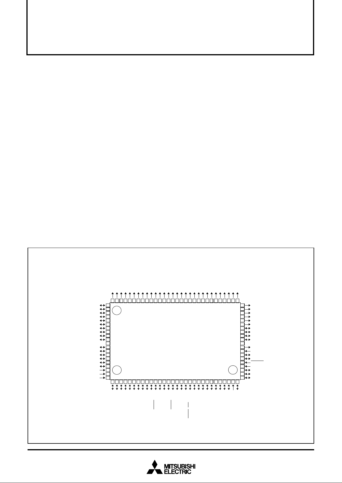
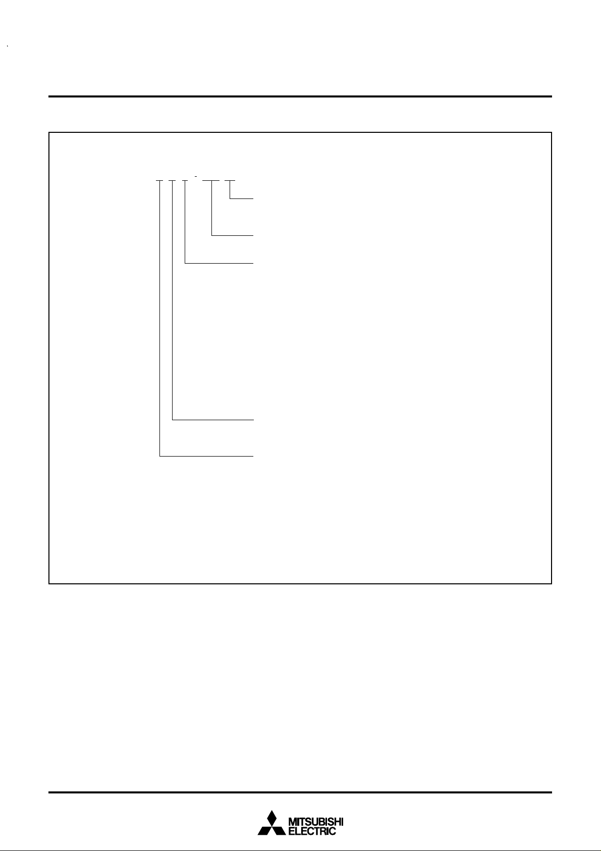
PIN CONFIGURATION (TOP VIEW)
19
18
17
16
/SEG
/SEG
/SEG
/SEG
3
2
1
0
P9
P9
P9
P9
77
78
79
80
AV
81
15
82
14
83
13
84
12
85
11
86
10
87
9
88
8
89
7
90
6
91
V
CC
92
5
93
4
94
3
95
2
96
1
97
0
98
V
EE
99
SS
100
V
REF
1
7
/AN
7
P7
2
6
/AN
6
P7
3
5
/AN
5
P7
4
4
/AN
4
P7
P87/SEG
P86/SEG
P85/SEG
P84/SEG
P83/SEG
P82/SEG
P81/SEG
P80/SEG
PA7/SEG
PA6/SEG
PA5/SEG
PA4/SEG
PA3/SEG
PA2/SEG
PA1/SEG
PA0/SEG
4
2
5
1
0
3
/DIG
/DIG
/DIG
/DIG
/DIG
20
/SEG
4
P9
76
21
/SEG
5
P9
75
22
/SEG
6
P9
74
23
/SEG
7
P9
73
24
/SEG
0
P3
72
25
/SEG
1
P3
71
26
/SEG
2
P3
70
27
/SEG
3
P3
69
28
/SEG
4
P3
68
29
/SEG
5
P3
67
30
/SEG
6
P3
66
31
/SEG
7
P3
65
32
/SEG
0
P0
64
33
/SEG
1
P0
63
34
/SEG
2
P0
62
/DIG
35
/SEG
3
P0
61
36
/SEG
4
P0
60
37
/SEG
5
P0
59
58
M38197MA-XXXFP
9
8
7
6
5
3
/AN
3
P7
2
/AN
2
P7
1
/AN
1
P7
0
/AN
0
P7
3
PB
10
/DA
2
PB
11
15
/AN
RDY3
/S
7
P5
12
14
/AN
CLK3
/S
6
P5
13
13
/AN
OUT3
/S
5
P5
14
12
/AN
IN3
/S
4
P5
15
11
/AN
RDY2
/S
3
P5
16
10
/AN
CLK2
/S
2
P5
17
9
/AN
OUT2
/S
1
P5
18
8
/AN
IN2
/S
0
P5
20
19
CLK12
/CS/S
RDY1
/S
7
CLK11
/S
6
P6
21
OUT1
/S
5
P6
23
22
IN1
/S
4
P6
P6
Package type : 100P6S-A
100-pin plastic-molded QFP
7
6
/DIG
/DIG
38
39
/SEG
/SEG
6
7
P0
P0
57
24
1
0
/CNTR
/CNTR
3
2
P6
P6
9
8
/DIG
/DIG
41
40
/SEG
/SEG
1
0
P1
P1
55
56
26
25
0
P6
/PWM
1
P6
10
/DIG
2
P1
54
27
OUT
/T3
7
P4
11
/DIG
3
P1
53
28
OUT
/T1
6
P4
12
/DIG
4
P1
52
29
/ZCR
1
/INT
5
P4
13
/DIG
5
P1
51
30
4
/INT
4
P4
50
49
48
47
46
45
44
43
42
41
40
39
38
37
36
35
34
33
32
31
P16/DIG
P17/DIG
P20/DIG
P21/DIG
P22/DIG
P23/DIG
P2
4
P2
5
P2
6
P2
7
V
SS
X
OUT
X
IN
PB0/X
PB1/X
RESET
P40/INT
P4
1
P42/INT
P43/INT
COUT
CIN
14
15
16
17
18
19
0
2
3
Page 2
MITSUBISHI MICROCOMPUTERS
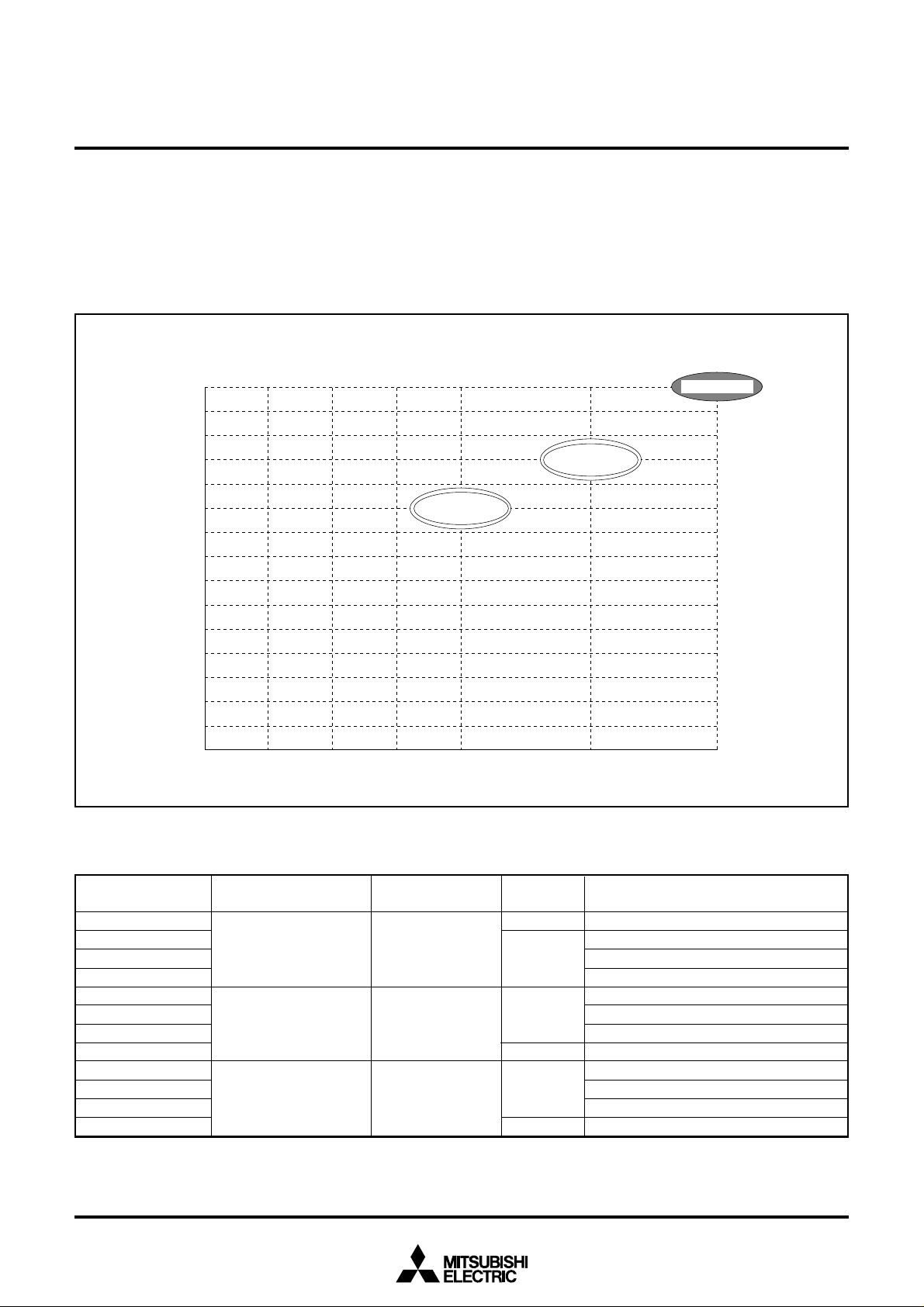
Interrupt interval
determination
circuit
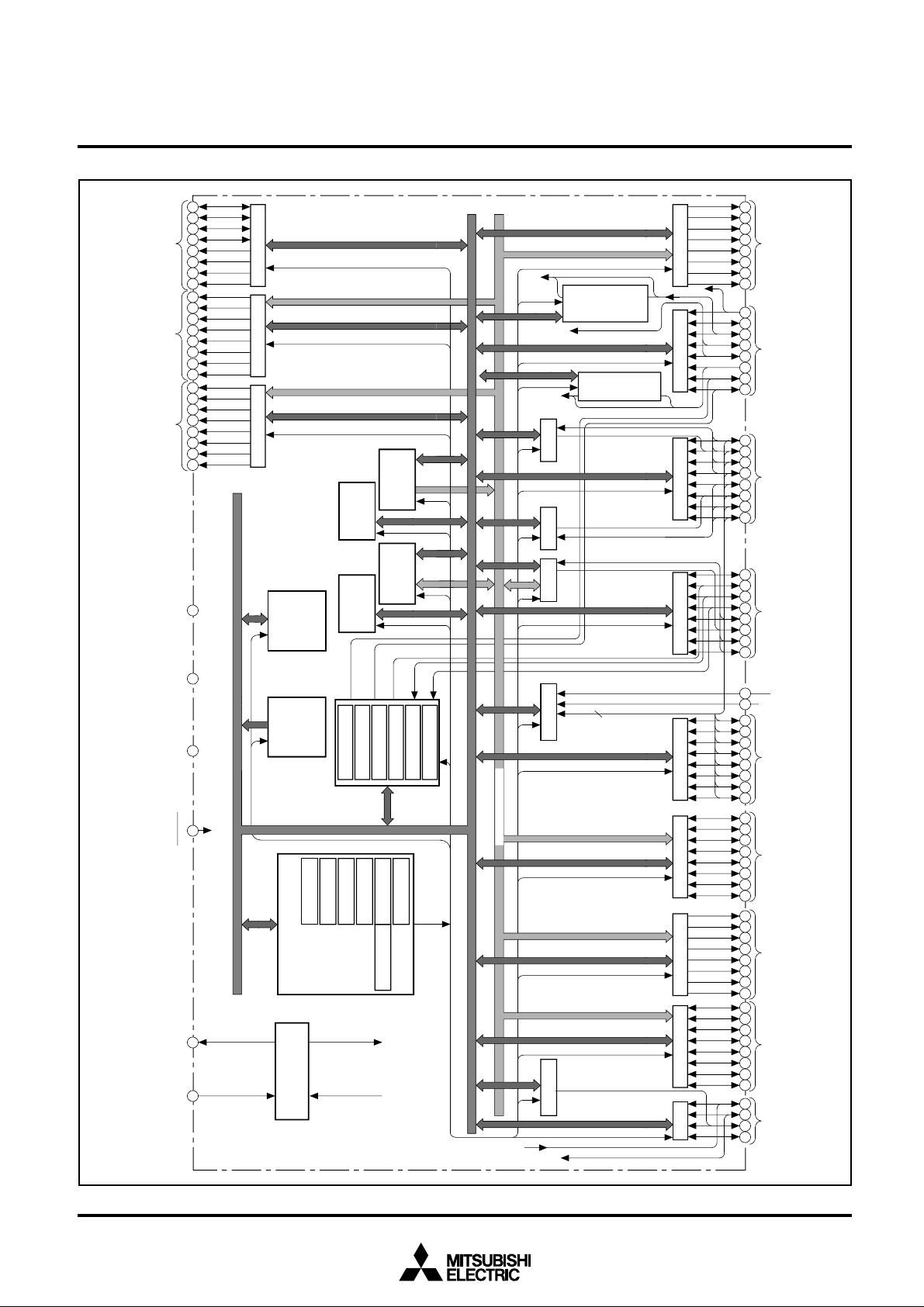
ROM
CPU
P7 (8)
I/O port P7
12345678
P8 (8)
I/O port P8
81 828384 85 8687 88
A-D
converter (8)
P9 (8)
Output port P9
7374 7576 77 7879 80
PA (8)
I/O port PA
8990 92 93 949596 97
PB (4)
I/O port PB
9103637
P6 (8)
I/O port P6
1920 21 22 2324 25 2699
100
AV
SS
VREF
P5 (8)
I/O port P5
11 12 13 14 1516 17 18
P4 (8)
I/O port P4(6)
Input port P4(2)
27 28 29 30 3132 33 34
P3 (8)
Output port P3
65 66 67 68 6970 7172
S I/O3(8)
S I/O2(8)S I/O1(8)
16
P2 (8)
Output port P2(4)
I/O port P2(4)
48 47 46 4544 43 42 41
P1 (8)
Output port P1
56 55 5453 52 515049
P0 (8)
Output port P0
64 63 62 6160 59 58 57
D-A
converter (8)
PS
PCL
S
Y
X
A
PCH
RAM
Data
bus
Timer 1 (8)
Timer 2 (8)
Timer 3 (8)
Timer 4 (8)
Timer 5 (8)
Timer 6 (8)
T1
OUT
SI/O
automatic
transfer
controller
FLD
automatic
display
controller
SI/O
automatic
transfer RAM
32 bytes
FLD
automatic
display RAM
96 bytes
Clock generating
circuit
X
COUT
Sub-clock
output
XCIN
Sub-clock
input
Clock
output
X
OUT
Clock
input
X
IN
92
VEE
40
(0 V)
V
SS
91
(5 V)
V
CC
35
Reset input
RESET
39
38
XCOUT
XCIN
Zero cross
detection circuit
INT
0
INT
1
/ZCR
INT
2
T3OUT
PWM
CNTR
0
CNTR1
Local data
bus
INT
3
, INT
4
3819 Group
SINGLE-CHIP 8-BIT CMOS MICROCOMPUTER
FUNCTIONAL BLOCK DIAGRAM (Package : 100P6S-A)
2
Page 3
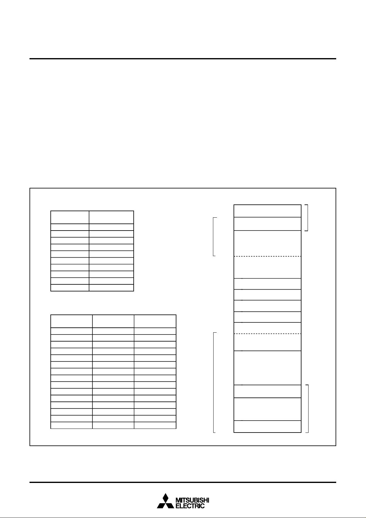
PIN DESCRIPTION
MITSUBISHI MICROCOMPUTERS
3819 Group
SINGLE-CHIP 8-BIT CMOS MICROCOMPUTER
Pin Name Function
VCC, VSS
VEE
VREF
AV SS
RESET
XIN
XOUT
P00/SEG32/
DIG0–P07/
SEG39/DIG7
P10/SEG40/
DIG8–P17/
DIG15
P20/DIG16–
P23/DIG19
P24–P27
P30/SEG24–
P37/SEG31
P40/INT0,
P45/INT1/
ZCR
P42/INT2–
P44/INT4
P41
P46/T1OUT,
P47/T3OUT
Power source
Pull-down
Power source
Analog reference
voltage
Analog power source
Reset input
Clock input
Clock output
Output port P0
Output port P1
Output port P2
I/O port P2
Output port P3
Input port P4
I/O port P4
•Apply voltage of 4.0 to 5.5 V to VCC, and 0 V to VSS.
•Applies voltage supplied to pull-down resistors of ports P0, P1, P20–P23, P3, and P9.
•Reference voltage input pin for A-D converter and D-A converter
•GND input pin for A-D converter and D-A converter
•Connect AVSS to VSS.
•Reset input pin for active “L”
•Input and output pins for the main clock generating circuit
•Feedback resistor is built in between XIN pin and XOUT pin.
•Connect a ceramic resonator or a quartz-crystal oscillator between the XIN pin and XOUT pin to
set oscillation frequency.
•If an external clock is used, connect the clock source to the XIN pin and leave the XOUT pin
open.
•This clock is used as the oscillating source of system clock.
•8-bit output port
•This port builds in pull-down resistor between
port P0 and the VEE pin.
•At reset this port is set to VEE level.
•The high-breakdown-voltage P-channel
open-drain
•8-bit output port with the same function as
port P0
•4-bit output port with the same function as
port P0
•4-bit I/O port
•I/O direction register allows each pin to be individually programmed as either input or output.
•At reset this port is set to input mode.
•TTL input level
•CMOS 3-state output
•8-bit output port with the same function as
port P0
•2-bit input port
•CMOS compatible input level
•6-bit CMOS I/O port with the same function
as ports P24–P27
•CMOS compatible input level
•CMOS 3-state output
Function except a port function
FLD automatic display pins
FLD automatic display pins
FLD automatic display pins
FLD automatic display pins
External interrupt input pins
A zero cross detection circuit input pin (P45)
Timer output pins
3
Page 4
PIN DESCRIPTION (Continued)
MITSUBISHI MICROCOMPUTERS
3819 Group
SINGLE-CHIP 8-BIT CMOS MICROCOMPUTER
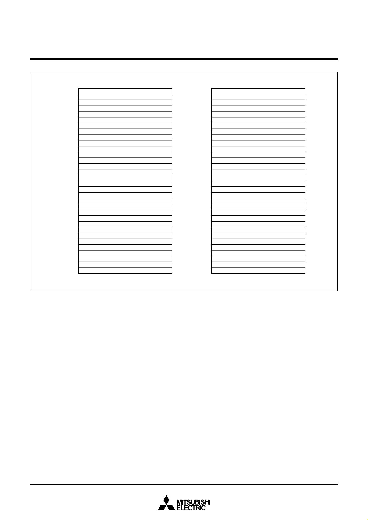
Pin Name Function
P50/SIN2/AN8,
P51/SOUT2/AN9,
P52/SCLK2/AN10,
P53/SRDY2/AN11
P54/SIN3/AN12,
P55/SOUT3/AN13,
P56/SCLK3/AN14,
P57/SRDY3/AN15
P60
P61/PWM
P62/CNTR0,
P63/CNTR1
P64/SIN1,
P65/SOUT1,
P66/SCLK11,
P67/SRDY1/CS/
SCLK12
P70/AN0–
P77/AN7
P80/SEG8–
P87/SEG15
P90/SEG16–
P97/SEG23
PA0/SEG0–
PA7/SEG7
I/O port P5
I/O port P6
I/O port P7
I/O port P8
Output port P9
I/O port PA
•8-bit CMOS I/O port with the same function
as ports P24–P27
•CMOS compatible input level
•CMOS 3-state output
•8-bit CMOS I/O port with the same function
as ports P24–P47
•CMOS compatible input level
•CMOS 3-state output
•8-bit CMOS I/O port with the same function
as ports P24–P27
•CMOS compatible input level
•CMOS 3-state output
•8-bit I/O port with the same function as ports
P24–P27
•CMOS compatible input level
•The high-breakdown-voltage P-channel
open-drain
•8-bit output port with the same function as
port P0
•8-bit I/O port with the same function as ports
P24–P27
•CMOS compatible input level
•The high-breakdown voltage P-channel open-
drain
Function except a port function
Serial I/O2 function pins
A-D conversion input pins
Serial I/O3 function pins
A-D conversion input pins
PWM output pin (Timer output pin)
Timer input pins
Serial I/O1 function pins
A-D conversion input pins
FLD automatic display pins
PB0/XCOUT,
PB1/XCIN
PB2/DA
PB3
I/O port PB
•4-bit CMOS I/O port with the same function
as ports P24–P27
•CMOS compatible input level
•CMOS 3-state output
I/O pins for sub-clock generating circuit (connect a ceramic resonator or a quarts-crystal
oscillator)
D-A conversion output pin
4
Page 5
PART NUMBERING
MITSUBISHI MICROCOMPUTERS
3819 Group
SINGLE-CHIP 8-BIT CMOS MICROCOMPUTER
Product M3819 FPM
A XXX7
Package type
FP : 100P6S-A package
FS : 100D0 package
ROM number
Omitted in some types.
ROM/PROM size
: 4096 bytes
1
: 8192 bytes
2
: 12288 bytes
3
: 16384 bytes
4
: 20480 bytes
5
: 24576 bytes
6
: 28672 bytes
7
: 32768 bytes
8
: 36864 bytes
9
: 40960 bytes
A
: 45056 bytes
B
: 49152 bytes
C
: 53248 bytes
D
: 57344 bytes
E
: 61440 bytes
F
The first 128 bytes and the last 2 bytes of ROM are reserved areas ; they cannot be used.
Memory type
M
: Mask ROM version
E
: EPROM or One Time PROM version
RAM size
0 : 192 bytes
1 : 256 bytes
2 : 384 bytes
3 : 512 bytes
4 : 640 bytes
5 : 768 bytes
6 : 896 bytes
7 : 1024 bytes
8 : 1536 bytes
9 : 2048 bytes
5
Page 6
MITSUBISHI MICROCOMPUTERS
3819 Group
SINGLE-CHIP 8-BIT CMOS MICROCOMPUTER
GROUP EXPANSION
Mitsubishi plans to expand the 3819 group as follows:
(1) Support for mask ROM, One Time PROM, and EPROM ver-
sions
ROM/PROM capacity .................................. 40 K to 60 K bytes
RAM capacity.............................................. 1024 to 2048 bytes
Memory Expansion Plan
60K
56K
52K
48K
44K
40K
36K
32K
28K
24K
20K
16K
12K
8K
4K
ROM size (bytes)
Mass product
(2) Packages
100P6S-A........................... 0.65 mm-pitch plastic molded QFP
100D0........................... Ceramic LCC(built-in EPROM version)
Under development
M38199MF/EF
Mass product
M38198MC/EC
M38197MA
256 512 768 1,024
RAM size (bytes)
Products under development : the development schedule and specifications may be revised without notice.
1,536 2,048
Currently supported products are listed below. As of May 1996
M38197MA-XXXFP
M38197MA-XXXKP
M38198MC-XXXKP
M38199MF-XXXKP
M38198MC-XXXFP
M38198EC-XXXFP
M38198ECFP
M38198ECFS
M38199MF-XXXFP
M38199EF-XXXFP
M38199EFFP
M38199EFFS
(P) ROM size (bytes)
ROM size for User in ( )
40960
(40830)
49152
(49022)
61440
(61310)
RAM size (bytes) RemarksPackageProduct
Mask ROM version
Mask ROM version
Mask ROM version
1024
100P6S-A
100P6P-E
Mask ROM version
Mask ROM version
1536
100P6S-A
100D0
One Time PROM version
One Time PROM version (blank)
EPROM version
Mask ROM version
2048
100P6S-A
100D0
One Time PROM version
One Time PROM version (blank)
EPROM version
6
Page 7

MITSUBISHI MICROCOMPUTERS
3819 Group
SINGLE-CHIP 8-BIT CMOS MICROCOMPUTER
FUNCTIONAL DESCRIPTION
Central Processing Unit (CPU)
The 3819 group uses the standard 740 family instruction set. Refer to the table of 740 family addressing modes and machine
instructions or the 740 Family Software Manual for details on the
instruction set.
Machine-resident 740 family instructions are as follows:
The FST, SLW instruction cannot be used.
The MUL, DIV, WIT and STP instruction can be used.
b7
b0
CPU mode register
(CPUM (CM) : address 003B
CPU Mode Register
The CPU mode register is allocated at address 003B16. The CPU
mode register contains the stack page selection bit and the internal system clock selection bit.
16
)
Processor mode bits
b1 b0
0 0 : Single-chip mode
0 1 :
1 0 : Not available
1 1 :
Stack page selection bit
0 : RAM in the zero page is used as stack area
1 : RAM in page 1 is used as stack area
X
COUT
drivability selection bit
0 : Low drive
1 : High drive
Port X
C
switch bit
0 : I/O port function
1 : X
CIN-XCOUT
oscillating function
Main clock (X
0 : Oscillating
1 : Stopped
Main clock division ratio selection bit
0 : f(X
1 : f(X
Internal system clock selection bit
0 : X
1 : X
IN-XOUT
) stop bit
IN
)/2 (high-speed mode)
IN
)/8 (middle-speed mode)
IN-XOUT
selected (middle/high-speed mode)
CIN-XCOUT
selected (low-speed mode)
Fig. BA-1 Structure of CPU mode register
7
Page 8
MITSUBISHI MICROCOMPUTERS
3819 Group
SINGLE-CHIP 8-BIT CMOS MICROCOMPUTER
Memory
Special function register (SFR) area
The special function register (SFR) area in the zero page contains
control registers such as I/O ports and timers.
RAM
RAM is used for data storage and for stack area of subroutine
calls and interrupts.
ROM
The first 128 bytes and the last 2 bytes of ROM are reserved for
device testing and the reset is user area for storing programs.
Interrupt vector area
The interrupt vector area contains reset and interrupt vectors.
RAM area
RAM capacity
(bytes)
192
256
384
512
640
768
896
1024
1536
2048
ROM area
ROM capacity
(bytes)
4096
8192
12288
16384
20480
24576
28672
32768
36864
40960
45056
49152
53248
57344
61440
Address XXXX
00FF
16
013F
16
01BF
16
023F
16
02BF
16
033F
16
03BF
16
043F
16
063F
16
083F
16
Address YYYY
F000
16
E000
16
D000
16
C000
16
B000
16
A000
16
9000
16
8000
16
7000
16
6000
16
5000
16
4000
16
3000
16
2000
16
1000
16
16
16
Address ZZZZ
F080
16
E080
16
D080
16
C080
16
B080
16
A080
16
9080
16
8080
16
7080
16
6080
16
5080
16
4080
16
3080
16
2080
16
1080
16
16
Zero page
The 256 bytes from addresses 000016 to 00FF16 are called the
zero page area. The internal RAM and the special function registers (SFR) are allocated to this area.
The zero page addressing mode can be used to specify memory
and register addresses in the zero page area. Access to this area
with only 2 bytes is possible in the zero page addressing mode.
Special page
The 256 bytes from addresses FF0016 to FFFF16 are called the
special page area. The special page addressing mode can be
used to specify memory addresses in the special page area. Access to this area with only 2 bytes is possible in the special page
addressing mode.
16
0000
RAM
RO
M
0040
010016
XXXX
044016
0F00
0F1F16
0F80
0FDF16
YYYY
ZZZZ
FF00
FFDC
FFFE
FFFF
SFR area
16
16
Reserved area
Not used
16
RAM area for serial I/O automatic transfer
Not used
16
RAM area for FLD automatic display
Not used
16
Reserved ROM area
(common ROM area,128 bytes)
16
16
16
Interrupt vector area
16
16
Reserved ROM area
Zero
page
Special
page
Fig. CA-1 Memory map
8
Page 9
0000
0001
0002
0003
0004
0005
0006
0007
0008
0009
000A
000B
000C
000D
000E
000F
0010
0011
0012
0013
0014
0015
0016
0017
0018
0019
001A
001B
001C
001D
001E
001F
16
Port P0 (P0)
16
16
Port P1 (P1)
16
16
Port P2 (P2)
16
Port P2 direction register (P2D)
16
Port P3 (P3)
16
16
Port P4 (P4)
16
Port P4 direction register (P4D)
Port P5 (P5)
16
Port P5 direction register (P5D)
16
Port P6 (P6)
16
Port P6 direction register (P6D)
16
Port P7 (P7)
16
Port P7 direction register (P7D)
16
Port P8 (P8)
16
Port P8 direction register (P8D)
16
16
Port P9 (P9)
16
16
Port PA (PA)
16
Port PA direction register (PAD)
Port PB (PB)
16
16
Port PB direction register (PBD)
Serial I/O automatic transfer data pointer (SIODP)
16
16
Serial I/O1 control register (SIO1CON)
16
Serial I/O automatic transfer control register (SIOAC)
16
Serial I/O1 register (SIO1)
Serial I/O automatic transfer interval register (SIOAI)
16
16
Serial I/O2 control register (SIO2CON)
16
Serial I/O3 control register (SIO3CON)
16
Serial I/O2 register (SIO2)
0020
0021
0022
0023
0024
0025
0026
0027
0028
0029
002A
002B
002C
002D
002E
002F
0030
0031
0032
0033
0034
0035
0036
0037
0038
0039
003A
003B
003C
003D
003E
003F
MITSUBISHI MICROCOMPUTERS
3819 Group
SINGLE-CHIP 8-BIT CMOS MICROCOMPUTER
16
Timer 1 (T1)
Timer 2 (T2)
16
Timer 3 (T3)
16
Timer 4 (T4)
16
Timer 5 (T5)
16
Timer 6 (T6)
16
Serial I/O3 register (SIO3)
16
Timer 6 PWM register (T6PWM)
16
Timer 12 mode register (T12M)
16
Timer 34 mode register (T34M)
16
16
Timer 56 mode register (T56M)
16
D-A conversion register (DA)
16
AD-DA control register (ADCON)
16
A-D conversion register (AD)
16
16
Interrupt interval determination register (IID)
16
Interrupt interval determination control register (IIDCON)
16
16
Port P0 segment/digit switch register (P0SDR)
Port P2 digit/port switch register (P2DPR)
16
Port P8 segment/port switch register (P8SPR)
16
16
Port PA segment/port switch register (PASPR)
16
FLDC mode register 1 (FLDM1)
FLDC mode register 2 (FLDM2)
16
16
FLD data pointer (FLDDP)
Zero cross detection control register (ZCRCON)
16
Interrupt edge selection register (INTEDGE)
16
CPU mode register (CPUM)
16
Interrupt request register 1 (IREQ1)
16
Interrupt request register 2 (IREQ2)
16
Interrupt control register 1 (ICON1)
16
16
Interrupt control register 2 (ICON2)
Fig. CA-2 Memory map of special function register (SFR)
9
Page 10
MITSUBISHI MICROCOMPUTERS
3819 Group
SINGLE-CHIP 8-BIT CMOS MICROCOMPUTER
I/O PORTS
Direction Registers
The 3819 group has 54 programmable I/O pins arranged in 8 I/O
ports (ports P24–P27, P41–P44, P46, P47, P5–P8, PA, and PB).
The I/O ports have direction registers which determine the input/
output direction of each individual pin. Each bit in a direction register corresponds to one pin, each pin can be set to be input or
output.
When “0” is written to the bit corresponding to a pin, that pin becomes an input pin. When “1” is written to that bit, that pin
becomes an output pin.
If data is read from a pin which is set for output, the value of the
port latch is read, not the value of the pin itself. A pin which is set
for input the value of the pin itself is read because the pin is in
floating state. If a pin set for input is written to, only the port latch
is written to and the pin remains floating.
Pin Name Input/Output I/O Format Non-Port Function Related SFRS
P00/SEG32/
DIG0–
P07/SEG39/
DIG7
P10/SEG40/
DIG8–
P17/DIG15
P20/DIG16–
P23/DIG19
P24–P27
P30/SEG24–
P37/SEG31
P40/INT0
P45/INT1/
ZCR
P42/INT2–
P44/INT4
P41
P46/T1OUT,
P47/T3OUT
Port P0
Port P1
Port P2
Port P3
Port P4
Output
Output
Output
Input/output,
individual bits
Output
Input
Input/output,
individual bits
High-breakdownvoltage P-channel
open-drain output
with pull-down
resistor
High-breakdownvoltage P-channel
open-drain output
with pull-down
resistor
High-breakdownvoltage P-channel
open-drain output
with pull-down
resistor
TTL level input
CMOS 3-state output
High-breakdownvoltage P-channel
open-drain output
with pull-down
resistor
CMOS compatible
input level
CMOS compatible
input level
CMOS 3-state output
High-Breakdown-Voltage Output Ports
The 3819 group microprocessors have 7 ports with high-breakdown-voltage pins (ports P0, P1, P20–P23, P3, P8, P9, PA). The
high-breakdown-voltage ports have P-channel open-drain output
with VCC –40 V of breakdown voltage.
Each pin in ports P0, P1, P20–P23, P3, and P9 has an internal
pull-down resistor connected to VEE. Ports P8 and PA have no internal pull-down resistors, so that connect an external resistor to
each port. At reset, the P-channel output transistor of each port
latch is turned off, so it becomes VEE level (“L”) by the pull-down
resistor.
Writing “1” (weak drivability) to bit 7 of the FLDC mode register 1
(address 003616) shows the rising transition of the output transistors for reducing transient noise. At reset, bit 7 of the FLDC mode
register 1 is set to “0” (strong drivability).
FLDC mode register 1
FLD automatic display function
FLD automatic display function
FLD automatic display function
FLD automatic display function
External interrupt
input
Zero cross detection circuit input
(P45)
Timer output
FLDC mode register 2
Port P0
segment/digit
switch register
FLDC mode register 1
FLDC mode register 2
FLDC mode register 1
FLDC mode register 2
Port P2 digit/port
switch register
FLDC mode register 1
FLDC mode register 2
Interrupt edge
selection register
Zero cross detection
control register
Timer 12 mode register
Timer 34 mode register
Diagram
No.
(1)
(1)
(2)
(3)
(4)
(5)
(6)
(7)
(4)
(8)
10
Page 11
MITSUBISHI MICROCOMPUTERS
3819 Group
SINGLE-CHIP 8-BIT CMOS MICROCOMPUTER
Pin Name Input/Output I/O Format Non-Port Function Related SFRS
P50/SIN2/
AN8
P51/SOUT2/
AN9,
P52/SCLK2/
AN10
P53/SRDY2/
AN11
P54/SIN3/
AN12
P55/SOUT3/
AN13,
P56/SCLK3/
AN14
P57/SRDY3/
AN15
P60
P61/PWM
P62/CNTR0,
P63/CNTR1
P64/SIN1
P65/SOUT1,
P66/SCLK11
P67/SRDY1/
CS/SCLK12
P70/AN0–
P77/AN7
P80/SEG8–
P87/SEG15
P90/SEG16–
P97/SEG23
PA0/SEG0–
PA7/SEG7
PB0/XCOUT,
PB1/XCIN
PB2/DA
PB3
Note : Make sure that the input level at each pin is either 0 V or VCC during execution of the STP instruction. When an input level is at an intermediate poten-
tial, a current will flow from V
Port P5
Port P6
Port P7
Port P8
Port P9
Port PA
Port PB
Input/output,
individual bits
Output
Input/output,
individual bits
Input/output,
individual bits
CC to VSS through the input-stage gate.
CMOS compatible
input level
CMOS 3-state output
CMOS compatible
input level
CMOS 3-state output
CMOS compatible
input level
CMOS 3-state output
CMOS compatible
input level
High-breakdown-
voltage P-channel
open-drain output
with pull-down
resistor
High-breakdownvoltage P-channel
open-drain output
with pull-down
resistor
CMOS compatible
input level
High-breakdownvoltage P-channel
open-drain output
CMOS compatible
input level
CMOS 3-state output
Serial I/O2 function I/O
A-D conversion input
Serial I/O3 function I/O
A-D conversion input
PWM (timer) output
Timer input
Serial I/O1 function I/O
A-D conversion input
FLD automatic
display function
I/O for sub-clock
generating circuit
D-A conversion
output
Serial I/O2 control
register
AD/DA control register
Serial I/O3 control
register
AD/DA control register
Timer 56 mode register
Interrupt edge selection register
Serial I/O1 control
register
Serial I/O automatic
transfer control register
AD/DA control register
FLDC mode register
Segment/port switch
register
FLDC mode register
FLDC mode register
Segment/port switch
register
CPU mode register
AD/DA control regis-
ter
Diagram
No.
(9)
(10)
(11)
(9)
(10)
(11)
(4)
(8)
(7)
(9)
(10)
(11)
(12)
(13)
(5)
(13)
(14)
(15)
(16)
(4)
11
Page 12
MITSUBISHI MICROCOMPUTERS
3819 Group
SINGLE-CHIP 8-BIT CMOS MICROCOMPUTER
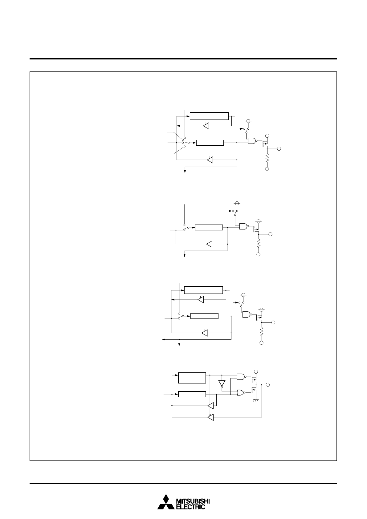
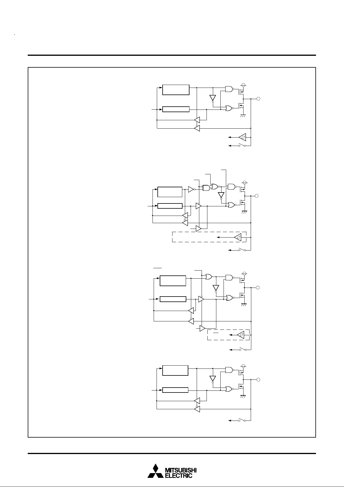
(1) Ports P0, P10, P1
(2) Ports P12–P1
(3) Ports P20–P2
7
3
1
Blanking signal
for key-scan
Data bus
Local data bus
Data bus
Shift signal from previous stage
S/D switch register
Dimmer signal
Port latch
Shift signal to next stage
Shift signal from previous stage
Dimmer signal
(Note)
Port latch
Shift signal to next stage
Shift signal from previous stage
D/P switch register
(Note)
✽
V
EE
✽
V
EE
(4) Ports P24–P27, P41, P60, PB
✽ : High-breakdown-voltage P-channel transistor
Note: The dimmer signal sets the Toff timing.
Fig. UA-2 Port block diagram (1)
Data bus
Blanking signal
for key-scan
Data bus
Shift signal to next stage
3
Direction
register
Port latch
Dimmer signal
Port latch
(Note)
✽
V
EE
12
Page 13
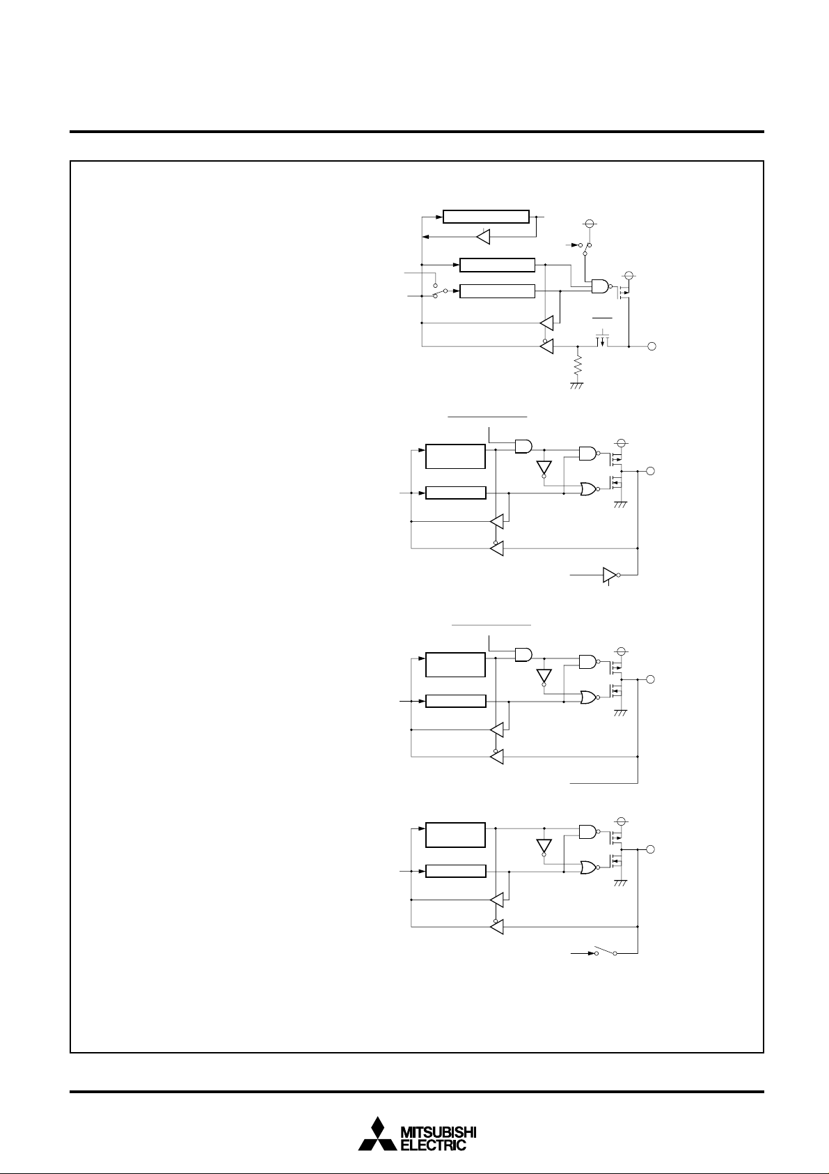
(5) Ports P3, P9
Local data bus
Data bus
MITSUBISHI MICROCOMPUTERS
3819 Group
SINGLE-CHIP 8-BIT CMOS MICROCOMPUTER
Dimmer signal
(Note)
Port latch
✽
V
EE
(6) Ports P40, P4
(7) Ports P4
5
2
–P44, P62, P6
(8) Ports P46, P47, P6
Data bus
0
, INT1 interrupt input
INT
Zero cross
detection
circuit
input
5
)
(only P4
3
Direction
register
Data bus
1
Port latch
2
–INT4 interrupt input
INT
0
,CNTR1 input
CNTR
Timer 1 output selection bit
Timer 3 output selection bit
Timer 6 output selection bit
Direction
register
✽ : High-breakdown-voltage P-channel transistor
Note: The dimmer signal sets the Toff timing.
Fig. UA-3 Port block diagram (2)
Data bus
Port latch
Timer 1 output
Timer 3 output
Timer 6 output
13
Page 14
MITSUBISHI MICROCOMPUTERS
3819 Group
SINGLE-CHIP 8-BIT CMOS MICROCOMPUTER
(9) Ports P50, P54, P6
(10) Ports P51, P52, P55, P56, P65, P6
(11) Ports P53, P57, P6
4
Data bus
Data bus
7
Direction
register
Port latch
6
P-channel output disable signal
Output OFF control signal
Serial I/O port selection bit
Direction
register
Port latch
OUT
or S
CLK
S
S
RDY
output enable bit
Direction
register
Serial I/O input
A-D conversion input
Analog input pin selection bit
Serial clock input
(only P52, P56, P66)
A-D conversion input
Analog input pin selection bit
(12) Port P7
Fig. UA-4 Port block diagram (3)
Data bus
Port latchData bus
Serial ready output
CLK
or S
A-D conversion input
Direction
register
Port latch
A-D conversion input
CS input
(only P67)
Analog input pin selection bit
Analog input pin selection bit
14
Page 15
MITSUBISHI MICROCOMPUTERS
3819 Group
SINGLE-CHIP 8-BIT CMOS MICROCOMPUTER
(13) Ports P8, PA
(14) Port PB0
Local
data bus
Data bus
Data bus
S/P switch register
Directionregister
Port latch
C switch
Port X
bit
Direction
register
Port latch
Dimmer signal
(Note)
Port PB
rea
d
Oscillation circuit
1
Port XC switch bit
✽
(15) Port PB1
(16) Port PB2
✽ : High-breakdown-voltage P-channel transistor
Note: The dimmer signal sets the Toff timing.
Data bus
Data bus
C switch
Port X
bit
Direction
register
Port latch
Sub-clock generating circuit input
Direction
register
Port latch
D-A conversion output
D-A output enable bit
Fig. UA-5 Port block diagram (4)
15
Page 16
MITSUBISHI MICROCOMPUTERS
3819 Group
SINGLE-CHIP 8-BIT CMOS MICROCOMPUTER
INTERRUPTS
Interrupts occur by 20 sources: 5 external, 14 internal, and 1 software.
Interrupt Control
Each interrupt is controlled by an interrupt request bit, an interrupt
enable bit, and the interrupt disable flag except for the software interrupt set by the BRK instruction. An interrupt occurs if the
corresponding interrupt request and enable bits are “1” and the interrupt disable flag is “0”.
Interrupt enable bits can be set or cleared by software.
Interrupt request bits can be cleared by software, but cannot be
set by software.
The BRK instruction cannot be disabled with any flag or bit.
The I (interrupt disable) flag disables all interrupts except the BRK
instruction interrupt.
Table 1. Interrupt vector addresses and priority
Interrupt Source Priority
Reset (Note 2) Non-maskable
INT0
INT1/ZCR
INT2
Remote control/
counter overflow
Serial I/O1
Serial I/O
automatic transfer
Serial I/O2
Serial I/O3
Timer 1
Timer 2
Timer 3
Timer 4
Timer 5
Timer 6
INT3
INT4
A-D conversion
FLD blanking
FLD digit
BRK instruction
Notes 1 : Vector addresses contain interrupt jump destination addresses.
2 : Reset function in the same way as an interrupt with the highest priority.
1
2
3
4
5
6
7
8
9
10
11
12
13
14
15
16
17
Vector Addresses (Note 1)
High
FFFD16
FFFB16
FFF916
FFF716
FFF516
FFF316
FFF116
FFEF16
FFED16
FFEB16
FFE916
FFE716
FFE516
FFE316
FFE116
FFDF16
FFDD16
Low
FFFC16
FFFA16
FFF816
FFF616
FFF416
FFF216
FFF016
FFEE16
FFEC16
FFEA16
FFE816
FFE616
FFE416
FFE216
FFE016
FFDE16
FFDC16
Interrupt Operation
When an interrupt is received, the contents of the program counter
and processor status register are automatically stored into the
stack. The interrupt disable flag is set to inhibit other interrupts
from interfering. The corresponding interrupt request bit is cleared
and the interrupt jump destination address is read from the vector
table into the program counter.
Notes on Use
When the active edge of an external interrupt (INT0 to INT4) is
changed or when switching interrupt sources in the same vector
address, the corresponding interrupt request bit may also be set.
Therefore, please take following sequence;
(1) Disable the external interrupt which is selected.
(2) Change the active edge.
(3) Clear the interrupt request bit which is selected to “0”.
(4) Enable the external interrupt which is selected.
Interrupt Request
Generating Conditions
At reset
At detection of either rising or
falling edge of INT0 input
At detection of either rising or
falling edge of INT1/ZCR input
At detection of either rising or
falling edge of INT2 input
At 8-bit counter overflow
At completion of data transfer
At completion of the last data
transfer
At completion of data transfer
At completion of data transfer
At timer 1 underflow
At timer 2 underflow
At timer 3 underflow
At timer 4 underflow
At timer 5 underflow
At timer 6 underflow
At detection of either rising or
falling edge of INT3 input
At detection of either rising or
falling edge of INT4 input
At completion of A-D conversion
At falling edge of the last digit
immediately before blanking
period starts
At rising edge of each digit
At BRK instruction execution
External interrupt (active edge
selectable)
External interrupt (active edge
selectable)
External interrupt (active edge
selectable)
Valid when interrupt interval
determination is operating
Valid when serial I/O ordinary
mode is selected
Valid when serial I/O automatic
transfer mode is selected
Valid when serial I/O2 is selected
Valid when serial I/O3 is selected
STP release timer underflow
External interrupt (active edge
selectable)
Valid when INT4 interrupt is
selected
External interrupt (active
edge selectable)
Valid when A-D conversion interrupt is selected
Valid when FLD blanking interrupt is selected
Valid when FLD digit interrupt
is selected
Non-maskable software interrupt
Remarks
16
Page 17
Interrupt request bit
Interrupt enable bit
Interrupt disable flag (I)
MITSUBISHI MICROCOMPUTERS
3819 Group
SINGLE-CHIP 8-BIT CMOS MICROCOMPUTER
Fig. DD-1 Interrupt control
b7
b7
b0
Interrupt edge selection register
(INTEDGE : address 003A
0
interrupt edge selection bit
INT
INT
1
/ZCR interrupt edge selection bit
2
interrupt edge selection bit
INT
INT
3
interrupt edge selection bit
4
interrupt edge selection bit
INT
INT
4
/AD conversion interrupt switch bit
CNTR
0
pin active edge switch bit
CNTR
1
pin active edge switch bit
b0
Interrupt request register 1
(IREQ1 : address 003C
0
interrupt request bit
INT
INT
1
/ZCR interrupt request bit
2
interrupt request bit
INT
Remote control/counter overflow
interrupt request bit
Serial I/O1 interrupt request bit
Serial I/O automatic transfer
interrupt request bit
Serial I/O2 interrupt request bit
Serial I/O3 interrupt request bit
Timer 1 interrupt request bit
Timer 2 interrupt request bit
16
16
)
BRK instruction
)
Reset
0 : Falling edge active
1 : Rising edge active
4
interrupt
0 : INT
1 : A-D conversion interrupt
0 : Rising edge count
1 : Falling edge count
b7
0 : No interrupt request issued
1 : Interrupt request issued
Interrupt request
b0
Interrupt request register 2
(IREQ2 : address 003D
Timer 3 interrupt request bit
Timer 4 interrupt request bit
Timer 5 interrupt request bit
Timer 6 interrupt request bit
INT
3
interrupt request bit
INT
4
interrupt request bit
AD conversion interrupt request bit
FLD blanking interrupt request bit
FLD digit interrupt request bit
Not used (returns “0” when read)
16
)
b7
b0
Interrupt control register 1
(ICON1 : address 003E
0
interrupt enable bit
INT
1
/ZCR interrupt enable bit
INT
INT
2
interrupt enable bit
Remote control/counter overflow
interrupt enable bit
Serial I/O1 interrupt enable bit
Serial I/O automatic transfer
interrupt enable bit
Serial I/O2 interrupt enable bit
Serial I/O3 interrupt enable bit
Timer 1 interrupt enable bit
Timer 2 interrupt enable bit
Fig. DD-2 Structure of interrupt-related registers
b7
16
)
b0
Interrupt control register 2
(ICON2 : address 003F
16
)
Timer 3 interrupt enable bit
Timer 4 interrupt enable bit
Timer 5 interrupt enable bit
Timer 6 interrupt enable bit
INT
3
interrupt enable bit
4
interrupt enable bit
INT
AD conversion interrupt enable bit
FLD blanking interrupt enable bit
FLD digit interrupt enable bit
Not used (returns “0” when read)
(do not write “1” to this bit)
0 : Interrupts disabled
1 : Interrupts enabled
17
Page 18

TIMERS
The 3819 group has 6 built-in timers: timer 1, timer 2, timer 3,
timer 4, timer 5, and timer 6.
Each timer has the 8-bit timer latch. The timers count down.
Once a timer reaches 0016, at the next count pulse the contents of
each timer latch is loaded into the corresponding timer, and sets
the corresponding interrupt request bit to “1”.
The count can be stopped by setting the stop bit of each timer to
“1”. The internal clock φ can be set to either the high-speed mode
or low-speed mode with the CPU mode register. At the same time,
timer internal count source is switched to either f(XIN) or f(XCIN).
Timer 1 and Timer 2
The count sources of timer 1 and timer 2 can be selected by setting the timer 12 mode register. A rectangular waveform of timer 1
underflow signal divided by 2 is output from the P46/T1OUT pin.
The waveform polarity changes each time timer 1 overflows. The
active edge of the external clock CNTR0 can be switched with the
bit 6 of the interrupt edge selection register.
At reset or when executing the STP instruction, all bits of the timer
12 mode register are cleared to “0”, timer 1 is set to “FF16”, and
timer 2 is set to “0116”.
MITSUBISHI MICROCOMPUTERS
3819 Group
SINGLE-CHIP 8-BIT CMOS MICROCOMPUTER
Timer 3 and Timer 4
The count sources of timer 3 and timer 4 can be selected by setting the timer 34 mode register. A rectangular waveform of timer 3
underflow signal divided by 2 is output from the P47/T3OUT pin.
The waveform polarity changes each time timer 3 overflows.
The active edge of the external clock CNTR1 can be switched with
the bit 7 of the interrupt edge selection register.
Timer 5 and Timer 6
The count sources of timer 5 and timer 6 can be selected by setting the timer 56 mode register.
A rectangular waveform of timer 6 underflow signal divided by 2 is
output from the P61/PWM pin. The waveform polarity changes
each time timer 6 overflows.
Timer 6 PWM Mode
Timer 6 can output a rectangular waveform with duty cycle n/(n +
m) from the P61/PWM pin by setting the timer 56 mode register
(refer to fig. FB-3). The n is the value set in timer 6 latch (address
002516) and m is the value in the timer 6 PWM register (address
002716). If n is “0”, the PWM output is “L”, if m is “0”, the PWM output is “H”(n=0 is prior than m=0). In the PWM mode, interrupts
occur at the rising edge of the PWM output.
18
Page 19

XCIN
XIN
6/T1OUT
P4
P62/CNTR0
Internal system
clock selection
“1”
bit
1/16
“0”
P4
6 latch
1/2
Timer 1 output
selection bit
P46 direction register
Rising/falling
edge switch
“00”
“01”
“1”
“0”
“10”
Timer 1
count
source
selection bit
Timer 1
count stop
bit
Timer 2
count
source
selection bit
Timer 2
count stop
bit
SINGLE-CHIP 8-BIT CMOS MICROCOMPUTER
Timer 1 latch (8)
Timer 1 (8)
Timer 2 latch (8)
Timer 2 (8)
Data bus
FF
16
01
16
MITSUBISHI MICROCOMPUTERS
3819 Group
RESET
STP instruction
Timer 1 interrupt request
Timer 2 interrupt request
P4
7/T3OUT
P63/CNTR1
P61/PWM
P4
Timer 3 output
selection bit
7 direction register
P4
Rising/falling
edge switch
Timer 6 output
selection bit
7 latch
1/2
P6
1 latch
Timer 3
count
source
selection bit
“1”
“0”
Timer 3
count stop bit
Timer 4
count
source
selection bit
“01”
“00”
“10”
Timer 4
count stop
bit
Timer 5
count
source
selection bit
“1”
“0”
Timer 5
count stop bit
Timer 6
count
source
selection bit
“01”
“00”
Timer 6
“10”
count stop
bit
Timer 6 PWM register (8)
PWM
“1”
“0”
1/2
Timer 6 operating
mode selection bit
Timer 3 latch (8)
Timer 3 (8)
Timer 4 latch (8)
Timer 4 (8)
Timer 5 latch (8)
Timer 5 (8)
Timer 6 latch (8)
Timer 6 (8)
Timer 3 interrupt request
Timer 4 interrupt request
Timer 5 interrupt request
Timer 6 interrupt request
Fig. FB-1 Timer block diagram
1 direction register
P6
19
Page 20
MITSUBISHI MICROCOMPUTERS
3819 Group
SINGLE-CHIP 8-BIT CMOS MICROCOMPUTER
b7
b0
Timer 12 mode register
(T12M : address 0028
16
)
Timer 1 count stop bit
0 : Operating
1 : Stopped
Timer 2 count stop bit
0 : Operating
1 : Stopped
Timer 1 count source selection bit
0 : f(X
IN
1 : f(X
)/16 or f(X
CIN
CIN
)/16
)
Not used (returns “0” when read)
Timer 2 count source selection bits
b5 b4
0 0 : Timer 1 underflow
0 1 : f(X
1 0 : External count input CNTR
CIN
)
0
1 1 : Not available
Timer 1 output selection bit (P4
6
)
0 : I/O port
1 : Timer 1 output
Not used (returns “0” when read)
b7
b0
Timer 56 mode register
(T56M : address 002A
16
)
b7 b0
Timer 34 mode register
16
(T34M : address 0029
)
Timer 3 count stop bit
0 : Operating
1 : Stopped
Timer 4 count stop bit
0 : Operating
1 : Stopped
Timer 3 count source selection bit
0 : f(X
IN
)/16 or f(X
CIN
)/16
1 : Timer 2 underflow
Not used (returns “0” when read)
Timer 4 count source selection bits
b5 b4
0 0 : f(X
IN
)/16 or f(X
CIN
)/16
0 1 : Timer 3 underflow
1 0 : External count input CNTR
1 1 : Not available
Timer 3 output selection bit (P4
7
)
0 : I/O port
1 : Timer 3 output
Not used (returns “0” when read)
1
Timer 5 count stop bit
0 : Operating
1 : Stopped
Timer 6 count stop bit
0 : Operating
1 : Stopped
Timer 5 count source selection bit
0 : f(X
IN
)/16 or f(X
CIN
)/16
1 : Timer 4 underflow
Timer 6 operation mode selection bit
0 : Timer mode
1 : PWM mode
Timer 6 count source selection bits
b5 b4
0 0 : f(X
IN
)/16 or f(X
CIN
)/16
0 1 : Timer 5 underflow
1 0 : Timer 4 underflow
1 1 : Not available
Timer 6 (PWM) output selection bit (P6
1
)
0 : I/O port
1 : Timer 6 output
Not used (returns “0” when read)
(do not write “1”)
Fig. FB-2 Structure of timer-related registers
20
Page 21
Timer 6
count
source
Timer 6
PWM output
MITSUBISHI MICROCOMPUTERS
3819 Group
SINGLE-CHIP 8-BIT CMOS MICROCOMPUTER
ts
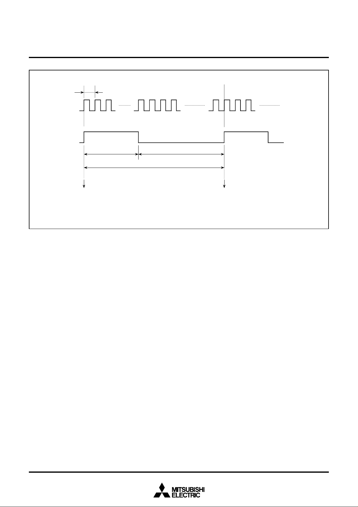
n ✕ ts m ✕ ts
(n + m) ✕ ts
Timer 6 interrupt request Timer 6 interrupt request
Note: If the value set in timer 6 is n and the value set in the timer 6 PWM register is m, a PWM waveform with
duty cycle n/(n + m) and period (n + m) 5 t
Fig. FB-3 Timing in timer 6 PWM mode
s (ts : the frequency of the timer 6 count source) is output.
21
Page 22

SERIAL I/O
The 3819 group has built-in 8-bit clock synchronized serial I/O ✕ 3
channels (serial I/O1, serial I/O2, and serial I/O3).
Serial I/O1 builds in the automatic transfer function. The function
can be switched to the serial I/O ordinary mode with the serial I/O
automatic transfer control register (address 001A16).
Serial I/O2 and Serial I/O3 can be used only in the serial I/O ordinary mode.
The I/O pins of the serial I/O function are also used as I/O ports
P5 and P64–P67, and their operation is selected with the serial I/O
control registers (addresses 001916, 001D16, and 001E16).
Serial I/O Control Registers
(SIO1CON, SIO2CON, SIO3CON)
0019
16, 001D16, 001E16
Each of the serial I/O control registers (addresses 001916,
001D16, and 001E16) consists of 8 selection bits which control the
serial I/O function.
MITSUBISHI MICROCOMPUTERS
3819 Group
SINGLE-CHIP 8-BIT CMOS MICROCOMPUTER
22
Page 23

MITSUBISHI MICROCOMPUTERS
3819 Group
SINGLE-CHIP 8-BIT CMOS MICROCOMPUTER
XCIN
X
P67/SRDY1/
CLK12
CS/S
P66/SCLK11
P65/SOUT1
P64/SIN1
P53/SRDY2
P5
2/SCLK2
P51/SOUT2
P50/SIN2
Main
address bus
Internal
system clock
“1”
selection bit
IN
“0”
(Note)
P67 latch
S
CS
P6
6 latch
“0”
Serial I/O1 port selection bit
Serial I/O1 port selection bit
“0”
“1”
“1”
P6
5 latch
P53 latch
“0”
SRDY2
“1”
SRDY2 output selection bit
“0”
P52 latch
Serial I/O2 port selection bit
Serial I/O2 port selection bit
“0”
“1”
“1”
P5
1 latch
Local
address bus
Address decorder
Synchronous
clock selection
bit
RDY1
Synchronization
circuit
CLK1
External clock
S
Synchronous
clock selection
bit
Synchronization
circuit
SI/O automatic
transfer RAM
16 to 0F1F16)
(0F00
SI/O automatic
transfer data
pointer
SI/O automatic
transfer
controller
SI/O automatic transfer
interval register
1/8
1/16
1/32
1/64
1/128
1/256
Frequency divider
“1”
Internal synchronous
clock selection bit
“0”
Serial I/O counter 1(3)
Serial I/O shift register 1(8)
1/8
1/16
1/32
1/64
1/128
1/256
Frequency divider
“1”
Internal synchronous
clock selection bit
External clock
CLK2
S
“0”
Serial I/O counter 2(3)
Serial I/O shift register 2(8)
Main data
bus
Local data
bus
Serial I/O automatic
transfer interrupt request
Serial I/O1
interrupt request
Serial I/O2
interrupt request
P57/SRDY3
6/SCLK3
P5
Serial I/O3 port selection bit
P55/SOUT3
Serial I/O3 port selection bit
P54/SIN3
Note:
Selected with the synchronous clock selection bit, S
I/O1 control register), automatic transfer control bit, and synchronous clock output pin selection bit (these 2 bits are ofthe serial I/O
automatic transfer register).
Fig. GA-1 Serial I/O block diagram
P57 latch
“0”
SRDY3
“1”
SRDY2 output selection bit
“0”
P56 latch
“1”
“0”
5 latch
P5
“1”
1/8
1/16
1/32
1/64
1/128
1/256
Frequency divider
Synchronization
circuit
“1”
External clock
CLK3
S
Serial I/O counter 3(3)
Internal synchronous
clock selection bit
“0”
Serial I/O3
interrupt request
Serial I/O shift register 3(8)
RDY1 output selection bit, serial I/O1 port selection bit (these 3 bits are of the serial
23
Page 24

MITSUBISHI MICROCOMPUTERS
3819 Group
SINGLE-CHIP 8-BIT CMOS MICROCOMPUTER
b7
b0
Serial I/O1 control register
(SIO1CON(SC1) : address 0019
16
)
b7
Internal synchronous clock selection bits
b2 b1 b0
IN
)/8 or f(X
CIN
,and S
CIN
CIN
CIN
CIN
CIN
CLK12
)/8
)/16
)/32
)/64
)/128
)/256
5
, P66, and P6
✽
output pins
✽
7
)
0 0 0 : f(X
IN
0 0 1 : f(X
0 1 0 : f(X
0 1 1 : f(X
1 1 0 : f(X
1 1 1 : f(X
)/16 or f(X
IN
)/32 or f(X
IN
)/64 or f(X
IN
)/128 or f(X
IN
)/256 or f(X
Serial I/O1 port selection bit (P6
0 : I/O port
OUT1,SCLK11
1 : S
RDY1
output selection bit (P67)
S
0 : I/O port
1 : S
RDY1
✽
/CS
output pin (Note)
Transfer direction selection bit
0 : LSB first
1 : MSB first
Synchronous clock selection bit
0 : External clock
1 : Internal clock
5/SOUT1
P6
P-channel output disable bit
0 : CMOS output (in output mode)
1 : N-channel open-drain output
(in output mode)
b7
b0
Serial I/O3 control register
(SIO3CON(SC3) : address 001E
16
)
Internal synchronous clock selection bits
b2 b1 b0
IN
)/8 or f(X
CIN
0 0 0 : f(X
IN
0 0 1 : f(X
0 1 0 : f(X
0 1 1 : f(X
1 1 0 : f(X
1 1 1 : f(X
)/16 or f(X
IN
)/32 or f(X
IN
)/64 or f(X
IN
)/128 or f(X
IN
)/256 or f(X
Serial I/O3 port selection bit (P5
0 : I/O port
OUT3
and S
1 : S
RDY3
output selection bit (P57)
S
CLK3
0 : I/O port
RDY3
and S
1 : S
CLK3
)/8
CIN
)/16
CIN
)/32
CIN
)/64
CIN
CIN
output pins
output pins
)/128
)/256
5
and P56)
Transfer direction selection bit
0 : LSB first
1 : MSB first
Synchronous clock selection bit
0 : External clock
1 : Internal clock
5/SOUT3
P5
P-channel output disable bit
0 : CMOS output (in output mode)
1 : N-channel open-drain output
(in output mode)
✽
: Valid only in serial I/O automatic transfer mode.
Note: When the external clock is selected in the serial I/O1 automatic transfer mode, the S
b0
Serial I/O2 control register
(SIO2CON(SC2) : address 001D
Internal synchronous clock selection bits
b2 b1 b0
IN
0 0 0 : f(X
0 0 1 : f(X
0 1 0 : f(X
0 1 1 : f(X
1 1 0 : f(X
1 1 1 : f(X
)/8 or f(X
IN
)/16 or f(X
IN
)/32 or f(X
IN
)/64 or f(X
IN
)/128 or f(X
IN
)/256 or f(X
Serial I/O2 port selection bit (P5
0 : I/O port
OUT2
and S
1 : S
RDY2
output selection bit (P53)
S
0 : I/O port
RDY2
1 : S
CLK2
output pin
Transfer direction selection bit
0 : LSB first
1 : MSB first
Synchronous clock selection bit
0 : External clock
1 : Internal clock
1/SOUT2
P5
P-channel output disable bit
0 : CMOS output (in output mode)
1 : N-channel open-drain output
(in output mode)
RDY1
signal pin becomes the CS signal input pin.
CIN
)/8
CIN
)/16
CIN
)/32
CIN
)/64
CIN
)/128
CIN
)/256
output pins
16
)
1
, and P52)
Fig. GA-2 Structure of serial I/O control registers
24
Page 25

MITSUBISHI MICROCOMPUTERS
3819 Group
SINGLE-CHIP 8-BIT CMOS MICROCOMPUTER
(1) Serial I/O Ordinary Mode
Either an internal clock or an external clock can be selected
as the synchronous clock for serial I/O transfer. A dedicated
divider is built in as the internal clock for selecting of 6 clocks.
If internal clock is selected, transfer starts with a write signal
to a serial I/O register (addresses 001B16, 001F16, or
002616). After 8 bits have been transferred, the SOUT pin goes
to high impedance state.
Synchronous
clock
Transfer clock
Serial I/O register
write signal
Serial I/O output
Serial I/O input
Receive enable
S
OUT
S
signal
S
RDY
IN
If external clock is selected, control the clock externally because the contents of the serial I/O register continue to shift
during inputting the transfer clock. In this case, note that the
SOUT pin does not go to high impedance state at the completion of data transfer.
The interrupt request bit is set at the completion of the transfer of 8 bits, regardless of whether the internal or external
clock is selected.
(Note)
D
1
D
0
D2D3D4D5D
6
D
7
OUT
Note :
If internal clock is selected, the S
at the completion of data transfer.
pin goes to high impedance state
Fig. GA-3 Serial I/O timing in the serial I/O ordinary mode (for LSB first)
(2) Serial I/O Automatic Transfer Mode
The serial I/O1 has the automatic transfer function. For automatic transfer, switch to the automatic transfer mode by
setting the serial I/O automatic transfer control register (address 001A16).
The following memory spaces and registers used to enable
automatic transfer mode:
• 32-byte serial I/O automatic transfer RAM
• A serial I/O automatic transfer control register
• A serial I/O automatic transfer interval register
• A serial I/O automatic transfer data pointer
When using serial I/O automatic transfer, set the serial I/O1
control register (address 001916) in the same way as the serial I/O ordinary mode. However, note that when external
clock is selected, port P67 becomes the CS input pin by setting the bit 4 (the SRDY1 output selection bit ) of the serial I/O1
control register to “1”.
Serial I/O Automatic Transfer Control Register
(SIOAC) 001A
The serial I/O automatic transfer control register (address 001A16)
consists of 4 bits which control automatic transfer.
16
Interrupt request bit set
b7
b0
Serial I/O automatic transfer control register
(SIOAC : address 001A16)
Automatic transfer control bit
0 : Serial I/O ordinary mode
(serial I/O1 interrupt)
1 : Automatic transfer mode
(serial I/O1 automatic transfer interrupt)
Automatic transfer start bit
0 : Transfer completion
1 : Transferring(starts by writing “1”)
Transfer mode switch bit
0 : Fullduplex(transmit and receive)
mode
1 : Transmit-only mode
Synchronous clock output
pin selection bit
0 : S
CLK11
1 : S
CLK12
Not used (return “0” when read)
Fig. GA-4 Structure of serial I/O automatic transfer control register
25
Page 26
MITSUBISHI MICROCOMPUTERS
3819 Group
SINGLE-CHIP 8-BIT CMOS MICROCOMPUTER
Serial I/O Automatic Transfer Data Pointer
(SIODP) 0018
The serial I/O automatic transfer data pointer (address 001816)
consists of 5 bits which indicate addresses in serial I/O automatic
transfer RAM (the value which adds 0F0016 to the serial I/O automatic transfer data pointer is actual address in memory).
Set the value (the number of transfer data-1) to the serial I/O automatic transfer data pointer for specifying the storage address of
first data.
16
● Serial I/O Automatic Transfer RAM
The serial I/O automatic transfer RAM is the 32 bytes from address 0F0016 to address 0F1F16.
Address
0F00
0F01
0F02
Bit
76
16
16
16
543210
● Setting of Serial I/O Automatic Transfer
Data
When data is stored in the serial I/O automatic transfer RAM,
store the first data at the address set with the serial I/O automatic transfer data pointer so that the last data can be stored
at address 0F0016.
Serial I/O Automatic Transfer Interv al Register
(SIOAI) 001C
The serial I/O automatic transfer interval register (address
001C16) consists of a 5-bit counter that determines the transfer interval Ti during automatic transfer.
When writing the value n to the serial I/O automatic transfer interval register, Ti=(n+2) ✕ Tc (Tc: the length of one bit of the transfer
clock) occurs. However, note that this transfer interval setting is
valid only when selecting the internal clock as the clock source.
16
0F1D
16
0F1E
16
0F1F
16
Fig. GA-5 Bit allocation of serial I/O automatic transfer RAM
Transfer clock
Serial I/O output
Serial I/O input
OUT
S
S
IN
DO0DO1DO2DO3DO4DO5DO6DO
DI0DI1DI2DI3DI4DI5DI6DI
T
C
1-byte data
7
7
T
i
Fig. GA-6 Serial I/O automatic transfer interval timing
26
Page 27

MITSUBISHI MICROCOMPUTERS
3819 Group
SINGLE-CHIP 8-BIT CMOS MICROCOMPUTER
● Setting of Serial I/O Automatic Transfer
Timing
The timing of serial I/O automatic transfer is set with the serial
I/O1 control register (address 001916) and the serial I/O automatic transfer interval register (address 001C16).
The serial I/O1 control register sets the transfer clock speed,
and the serial I/O automatic transfer interval register sets the
serial I/O automatic transfer interval. This setting of transfer interval is valid only when selecting the internal clock as the
clock source.
● Start of Serial I/O Automatic Transfer
Automatic transfer mode is set by writing “1” to the bit 0 of the
serial I/O automatic transfer control register (address 001A16),
then automatic transfer starts by writing “1” to the bit 1.
The bit 1 of the serial I/O automatic transfer control register is
always “1” during automatic transfer; writing “0” can complete
the serial I/O automatic transfer.
● Operation in Serial I/O Automatic Transfer
Modes
There are two modes for serial I/O automatic transfer: full duplex mode and transmit-only mode. Either internal or external
clock can be selected for each of these modes.
(2.1) Operation in Full Duplex Mode
In full duplex mode, data can be transmitted and received at the
same time. Data in the automatic transfer RAM is transmitted in
sequence in accordance with the serial I/O automatic transfer data
pointer and simultaneously reception data is written to the automatic transfer RAM.
The transfer timing of each bit is the same as that in ordinary operation mode, and the transfer clock stops at “H” after eight
transfer clocks are counted.
When selecting the internal clock, the transfer clock remains at “H”
for the time set with the serial I/O automatic transfer interval register, then the data at the next address (the address is indicated with
the serial I/O automatic transfer data pointer) are transferred.
If when selecting the external clock, the setting of the automatic
transfer interval register is invalid, so control the transfer clock externally.
The last data transfer completes when the contents of the serial
I/O automatic transfer pointer reach “0016”. At that point, the serial
I/O automatic transfer interrupt request bit is set to “1” and the bit
1 of the serial I/O automatic transfer control register is cleared to
“0” to complete the serial I/O automatic transfer.
(2.2) Operation in Transmit-Only Mode
The operation in transmit-only mode is the same as that in full duplex mode, except for that data is not transferred from the serial
I/O1 register to the serial I/O automatic transfer RAM.
Transfer direction selection bit
Transfer clock
LSB first (SC1
MSB first (SC1
S
IN
Fig. GA-7 Serial I/O1 register transfer operation in full duplex mode
5
= “0” ) : MSB
5
= “1” ) : LSB
DO
DI
DI
DI
DI
LSB
MSB
7
DO
6
DO5DO
4
DO
3
DO2DO1DO
DO
7
DO6DO
0
1
DI
0
2
DI
1
7
DI
6
5
DO
4
DO3DO2DO
DO7DO6DO5DO4DO3DO
DO
7
DI
0
DI5DI4DI3DI2DI1DI
Serial I/O1 register
DO
6
DO5DO4DO
•
•
•
0
OUT
1
2
3
0
S
27
Page 28

MITSUBISHI MICROCOMPUTERS
3819 Group
SINGLE-CHIP 8-BIT CMOS MICROCOMPUTER
(2.3) When Selecting the Internal Clock
When selecting the internal clock, the P67/SRDY1/CS/SCLK12 pin
can be used as the SRDY1 pin by setting SC14 to “1”.
When selecting the internal clock, the P67 pin can be used as the
synchronous clock output pin SCLK12 by setting SIOAC3 to “1”. In
this case, the SCLK11 pin goes to high impedance state.
Select the function of the P67/SRDY1/CS/SCLK12 and P66/SCLK11
with the following registers (refer to Table GA-1):
●the bit 3 (SC13), the bit 4(SC14), and the bit 6(SC16) of the se-
rial I/O1 control register
● the bit 3 (SIOAC3) of the serial I/O automatic transfer control
register
Bit 1 write signal of serial I/O
automatic transfer control
register
Bit 1 of serial I/O automatic
transfer control register
Write signal from RAM to
serial I/O1 register
Write signal from serial I/O1
register to RAM
Data pointer
Transfer clock
CLK
(internal or S
output)
Receive
enabled signal
S
RDY
Serial I/O output
Serial I/O input
S
S
out
DO1DO2DO3DO4DO5DO6DO
DO
0
DI
0
IN
DI1DI2DI3DI4DI5DI6DI
When using both the SCLK11 and SCKL12 by switching, switch the
P67/SRDY1/CS/SCLK12 to the P67 (SC14=0) and set the P67 direction register to input mode. Note that switch SIOAC3 during “H” of
transfer clock at the completion of automatic transfer.
Table GA-1. SCLK11 and SCLK12 selection
SC161SC14
0
Note : SC13: Serial I/O1 port selection bit
4: SRDY1 output selection bit
SC1
6: Synchronous clock selection bit
SC1
3: Synchronous clock output pin selection bit
SIOAC
7
7
SC331SIOAC3
n-1
DO
DI
0n
0
DO
DI
0
0
1
6
6
DO
DI
7
7
P66/S
CLK11
SCLK11
High
impedance
P67/S
P67
SCLK12
CLK12
Transfer interval
Fig. GA-8 Timing diagram during serial I/O automatic transfer (internal clock selected, SRDY used)
Bit 1 write signal of serial I/O
automatic transfer control
register
Bit 1 of serial I/O automatic
transfer control register
Write signal from RAM to
serial I/O1 register
Write signal from serial I/O1
register to RAM
Bit 3 of serial I/O automatic
transfer control register
Data pointer
Transfer clock
(internal)
CLK11
output
S
CLK12
output
S
Serial I/O output
Serial I/O input
S
S
out
m
DO0
DO1 DO2 DO3
IN
DI0 DI1 DI2 DI3 DI4 DI5 DI6 DI
DO4
DO5 DO6 DO7 DO0 DO6 DO7 DO0 DO1 DO2 DO3
7
Transfer interval
m-1
0
DI0 DI0 DI1 DI2 DI
DI7
DI6
Fig. GA-9 Timing during serial I/O automatic transfer (internal clock selected, SCLK11 and SCLK12 used)
n
3
28
Page 29

MITSUBISHI MICROCOMPUTERS
3819 Group
SINGLE-CHIP 8-BIT CMOS MICROCOMPUTER
(2.4) When Selecting the External Clock
When selecting the external clock, the internal clock and the setting of transfer interval with the serial I/O automatic transfer
interval register are invalid, but the serial I/O output pin SOUT1 and
the internal transfer clock can be controlled from the outside by
setting the SRDY1 pin to the CS (input) pin.
When the CS input is “L”, the SOUT1 pin and the internal transfer
clock are enabled.
When the CS input is “H”, the SOUT1 pin goes to high impedance
state and the internal transfer clock goes to “H”.
Select the function of the P67/SRDY1/CS/SCLK12 with the following
registers (refer to Table GA-2):
●the bit 4 (SC14) and the bit 6 (SC16) of the serial I/O1 control
register
● the bit 0 (SIOAC0) of the serial I/O automatic transfer control
register
Switch the CS pin from “L” to “H” or from “H” to “L” during “H” of the
transfer clock (SCLK11 input) after transferring 1-byte data.
When selecting the external clock, set the external clock to “L” after 9 cycles or more of the internal clock φ after setting the start
bit. After transferring 1-byte data, leave 11 cycles or more of the
internal clock φ free for the transfer interval.
When not using the CS input, note that the SOUT pin will not go to
high impedance state, even after transfer is completed.
When not using the CS input, or when CS is “L”, control the external clock because the data in the serial I/O register will continue to
shift while the external clock is input, even after the completion of
automatic transfer (Note that the automatic transfer interrupt request bit is set and the bit 1 of the serial I/O automatic transfer
register is cleared at the point when the specified number of bytes
of data have been transferred.)
Table GA-2. P67/SRDY1/CS selection
SC160SC14
Note : SC14: SRDY1 output selection bit
6: Synchronous clock selection bit
SC1
0: Automatic transfer control bit
SIOAC
SIOAC0
0
1
✕
0
1
P67/SRDY1/CS
P67
SRDY1
CS
Bit 1 write signal of serial I/O
automatic transfer control
register
Bit 1 of serial I/O automatic
transfer control register
Write signal from RAM to
serial I/O1 register
Write signal from serial I/O1
register to RAM
Data pointer
External input
Transfer clock
CLK
input
S
Transfer clock
(internal)
Serial I/O output
Serial I/O input
OUT
S
S
CS
IN
n
X
DO
0
1DO2DO3DO4DO5DO6DO7
DO
DI0DI1DI2DI3DI4DI5DI6DI
Fig. GA-10 Timing during serial I/O automatic transfer (external clock selected)
n-1
7
X
Note: Data marked with X is invalid.
X
XX
X
29
Page 30

A-D CONVERTER
The functional blocks of the A-D converter are described below.
A-D Conversion Register (AD) 002D16
The A-D conversion register is a read-only register that stores the
result of an A-D conversion. This register should not be read during A-D conversion.
AD/DA Control Register (ADCON) 002C16
The AD/DA control register controls the A-D and the D-A conversion process. Bits 0 to 3 of this register select analog input pins.
Bit 4 is the AD conversion completion bit. The value of this bit remains at “0” during an A-D conversion, then changes to “1” when
the A-D conversion is completed.
The A-D conversion starts by writing “0” to this bit. Bit 6 controls
the output of D-A converter.
Comparison V oltage Generator
The comparison voltage generator divides the voltage between
AVSS and V REF by 256, and outputs the divided voltages.
Channel Selector
The channel selector selects one of the input ports P77/AN7–P70/
AN0, P57/SRDY3/AN15–P50/SIN2/AN8, and inputs to the comparator.
MITSUBISHI MICROCOMPUTERS
SINGLE-CHIP 8-BIT CMOS MICROCOMPUTER
b7
Fig. JA-1 Structure of A-D control register
b0
AD/DA control register
(ADCON : address 002C
Analog input pin selection bits
b3 b2 b1 b0
0 0 0 0 : P7
0 0 0 1 : P71/AN1
0 0 1 0 : P7
0 0 1 1 : P73/AN
0 1 0 0 : P74/AN
0 1 0 1 : P75/AN
0 1 1 0 : P76/AN
0 1 1 1 : P77/AN
1 0 0 0 : P50/S
1 0 0 1 : P51/S
1 0 1 0 : P52/S
1 0 1 1 : P53/S
1 1 0 0 : P54/S
1 1 0 1 : P55/S
1 1 1 0 : P56/S
1 1 1 1 : P57/S
AD conversion completion bit
0 : Conversion in progress
1 : Conversion completed
Not used (returns “0” when read)
DA output enable bit
0 : Disable
1 : Enable
Not used (returns “0” when read)
3819 Group
16
)
0
/AN
0
2
/AN
2
3
4
5
6
7
IN2
/AN
8
OUT2
/AN
9
CLK2
/AN
10
RDY2
/AN
11
IN3
/AN
12
OUT3
/AN
13
CLK3
/AN
14
RDY3
/AN
15
Comparator and Control Circuit
The comparator and control circuit compares an analog input voltage with the comparison voltage and stores the result in the A-D
conversion register. When an A-D conversion is completed, the
control circuit sets the AD conversion completion bit and the AD
conversion interrupt request bit to “1”.
Note that the comparator is constructed linked to a capacitor, so
set f(XIN) to 500 kHz or more during A-D conversion.
Note : When using the A-D conversion interrupt, set the INT4/AD conver-
sion interrupt switch bit (the bit 5 of the interrupt selection register)
to “1”.
30
Page 31

Data bus
MITSUBISHI MICROCOMPUTERS
3819 Group
SINGLE-CHIP 8-BIT CMOS MICROCOMPUTER
AD-DA control register
(address 002C
16
)
4
b7
A-D control circuit
P50/S
P51/S
P52/S
P53/S
P54/S
P55/S
P56/S
P57/S
P7
P71/AN
P72/AN
P73/AN
P74/AN
P75/AN
P76/AN
P77/AN
IN2
out2
CLK2
RDY2
IN3
OUT3
CLK3
RDY3
0
/AN
/AN
/AN
/AN
/AN
/AN
/AN
/AN
/AN
0
1
2
3
4
5
6
7
8
9
10
11
12
13
14
15
Channel selector
Comparator
Fig. JA-2 A-D converter block diagram
D-A CONVERTER
The 3819 group has internal D-A converter with 8-bit resolutions ✕
1 channel.
D-A conversion is performed by setting the value in the D-A conversion register. The result of D-A conversion is output from the
DA pin by setting the DA output enable bit to “1” . At this time, the
corresponding bit (PB2/DA) of the port PB direction register should
be set to “0” (input status).
The output analog voltage V is determined with the value n
(n: decimal number) in the D-A conversion register as follows:
b0
A-D conversion register
(Address 002D16)
8
Resistor ladder
REF
AV
V
SS
D-A conversion register (8)
Data bus
R-2R resistor ladder
A-D conversion interrupt request
DA output enable bit
PB2/DA
V=VREF ✕ n/256 (n=0 to 255)
✽VREF: the reference voltage
At reset, the D-A conversion register is cleared to “0016”, the DA
output enable bits are cleared to “0”, and the PB2/DA pin goes to
high impedance state. The D-A output does not build in a buffer, so
connect an external buffer when driving a low-impedance load.
Set VCC to 3.0 V or more when using the D-A converter.
"0"
PB2/DA
DA output enable bit
"1"
2R
R
2R 2R 2R 2R 2R 2R 2R
MSB
D-A conversion
register
V
AV
SS
REF
"0"
"1"
Fig. JB-2 Equivalent connection circuit of D-A converter
Fig. JB-1 D-A converter block diagram
RR RRRR
LSB
2R
31
Page 32

MITSUBISHI MICROCOMPUTERS
3819 Group
SINGLE-CHIP 8-BIT CMOS MICROCOMPUTER
FLD CONTROLLER
The 3819 group has fluorescent display (FLD) drive and control
circuits.
The FLD controller consists of the following components:
• 42 pins for segments
• 20 pins for digits
• FLDC mode register 1
• FLDC mode register 2
• FLD data pointer
• FLD data pointer reload register
Main
address bus
Local
address bus
Address
decoder
0F80
0F8F
0F90
0F9F
0FA0
0FAF
0FB0
0FBF
0FC0
0FCF
0FD0
0FDF
FLD automatic
display RAM
G1 (SEG PA)
16
G2 (SEG PA)
G15 (SEG PA)
G16 (SEG PA)
16
G1 (SEG P8)
16
G2 (SEG P8)
G15 (SEG P8)
G16 (SEG P8)
16
G1 (SEG P9)
16
G2 (SEG P9)
G15 (SEG P9)
G16 (SEG P9)
16
G1 (SEG P3)
16
G2 (SEG P3)
G15 (SEG P3)
G16 (SEG P3)
16
G1 (SEG P0)
16
G2 (SEG P0)
G15 (SEG P0)
G16 (SEG P0)
16
G1 (SEG P1)
16
G2 (SEG P1)
G15 (SEG P1)
G16 (SEG P1)
16
FLD data pointer
reload register
(address 0038
FLD data pointer
(address 003816)
Timing
generator
16
)
Main
data bus
• Port P0 segment/digit switch register
• Port P2 digit/port switch register
• Port PA segment/port switch register
• Port P8 segment/port switch register
• 96-byte FLD automatic display RAM
The segment pins can be used from 16 up to 42 pins (maximum)
and the digit pins can be used from 6 up to 16 pins (maximum).
The segment and the digit pins can be used up to 52 pins (maximum) in total.
In the FLD automatic display mode ports P12 to P17 become digit
pins DIG10 to DIG15 automatically.
Local
data bus
FLDC mode
register 1
(address 0036
PA0/SEG
S/P
PA1/SEG
S/P
PA
2
/SEG
S/P
PA
3
/SEG
S/P
4
/SEG
S/P
PA
PA
5
/SEG
S/P
PA
6
/SEG
S/P
PA
7
/SEG
S/P
0035
0034
0032
0014
16
P80/SEG
S/P
P81/SEG
S/P
P8
2
/SEG
S/P
3
/SEG
S/P
P8
P8
4
/SEG
S/P
P8
5
/SEG
S/P
P8
6
/SEG
S/P
7
/SEG
S/P
P8
0010
16
P90/SEG
P91/SEG
P92/SEG
P93/SEG
P94/SEG
P95/SEG
P96/SEG
P97/SEG
0012
P30/SEG
P31/SEG
P32/SEG
P33/SEG
P34/SEG
P35/SEG
P36/SEG
P37/SEG
0006
P00/SEG32/DIG
S/D
P01/SEG33/DIG
S/D
2
/SEG34/DIG
S/D
P0
P0
3
/SEG35/DIG
S/D
P0
4
/SEG36/DIG
S/D
P0
5
/SEG37/DIG
S/D
6
/SEG38/DIG
S/D
P0
P0
7
/SEG39/DIG
S/D
16
S/D
S/D
16
)
P20/DIG
D/P
P21/DIG
D/P
P2
D/P
P2
D/P
0033
16
FLD blanking interrupt
FLD digit interrupt
0
1
2
8
3
4
5
6
7
16
8
9
10
8
11
12
13
14
15
16
16
17
18
8
19
20
21
22
23
16
24
25
26
8
27
28
29
30
31
16
0
1
2
3
4
5
6
7
0000
P10/SEG40/DIG
P11/SEG41/DIG
P1
2
/DIG
P13/DIG
P14/DIG
P15/DIG
P16/DIG
P17/DIG
0037
16
16
17
2
/DIG
18
3
/DIG
19
0004
8
16
8
9
10
11
12
13
14
15
0002
8
16
4
16
Fig. KA-1 FLD control circuit block diagram
32
Page 33

MITSUBISHI MICROCOMPUTERS
3819 Group
SINGLE-CHIP 8-BIT CMOS MICROCOMPUTER
FLDC Mode Registers (FLDM 1, FLDM 2)
0036
16, 003716
The FLDC mode register 1 (address 003616) and FLDC mode register 2 (address 003716) are a seven bit register and an eight bit
b7
b0
FLDC mode register 1
(FLDM 1 : address 0036
T
scan
b1 b0
0 0 : 0 FLD digit interrupt (at rising edge of each digit)
0 1 : 1 ✕ T
1 0 : 2 ✕ T
1 1 : 3 ✕ T
T
off
control bits
(Setting of digit/segment OFF time)
b5 b4 b3 b2
0 0 0 0 : 1/16 ✕ T
0 0 0 1 : 2/16 ✕ T
0 0 1 0 : 3/16 ✕ T
0 0 1 1 : 4/16 ✕ T
0 1 0 0 : 5/16 ✕ T
0 1 0 1 : 6/16 ✕ T
0 1 1 0 : 7/16 ✕ T
0 1 1 1 : 8/16 ✕ T
1 0 0 0 : 9/16 ✕ T
1 0 0 1 : 10/16 ✕ T
1 0 1 0 : 11/16 ✕ T
1 0 1 1 : 12/16 ✕ T
1 1 0 0 : 13/16 ✕ T
1 1 0 1 : 14/16 ✕ T
1 1 1 0 : 15/16 ✕ T
1 1 1 1 : 16/16 ✕ T
Not used (returns “0” when read)
High-breakdown-voltage drivability selection bit
0 : Strong drivability
1 : Weak drivability
register respectively which are used to control the FLD automatic
display and set the blanking time Tscan for key-scan.
16
)
control bits
disp
FLD blanking interrupt
disp
(at falling edge of the last digit)
disp
disp
disp
disp
disp
disp
disp
disp
disp
disp
disp
disp
disp
disp
disp
disp
disp
Fig. KA-2 Structure of FLDC mode register 1
b7
b0
FLDC mode register 2
(FLDM 2 : address 0037
Automatic display control bit(P0, P1, P20–P23, P3, P8, P9, PA)
0 : Ordinary mode
16
)
1 : Automatic display mode
Display start bit
0 : Display stopped
1 : Display in progress
(display starts by writing “1” to this bit which is set to “0”)
T
disp
control bits
(digit time setting, at 8 MHz oscillation frequency)
b5 b4 b3 b2
0 0 0 0 : 128 µs
0 0 0 1 : 256 µs
0 0 1 0 : 384 µs
0 0 1 1 : 512 µs
0 1 0 0 : 640 µs
0 1 0 1 : 768 µs
0 1 1 0 : 896 µs
0 1 1 1 : 1024 µs
1 0 0 0 : 1152 µs
1 0 0 1 : 1280 µs
1 0 1 0
1 1 1 1
Pl
0
segment/digit switch bit
0 : Digit
1 : Segment
1
segment/digit switch bit
Pl
0 : Digit
Not available
1 : Segment
Fig. KA-3 Structure of FLDC mode register 2
33
Page 34
MITSUBISHI MICROCOMPUTERS
3819 Group
SINGLE-CHIP 8-BIT CMOS MICROCOMPUTER
● Pins for FLD Automatic Display
Ports P0, P1, P20–P23, P3, P8, P9, and PA is selected for the
FLD automatic display function by setting the automatic display
control bit of the FLDC mode register 2 (address 003716) to
“1”.
Table L-1. Pins in FLD automatic display mode
Port Name
PA0–PA7
P80–P87
P90–P97
P30–P37
P00–P07
P10, P11
P12–P17
P20–P23
Note : Be sure to set digits in sequence.
Automatic Display Pins
SEG0–SEG7
or
PA0–PA7
SEG8–SEG15
or
P80–P87
SEG16–SEG23
SEG24–SEG31
SEG32–SEG41
or
DIG0–DIG9
DIG10–DIG15
DIG16–DIG19
or
P20–P23
The individual bits of the segment/port switch register (address 003516) can be set each pin
to either segment (“1”) or general-purpose I/O port (“0”).
The individual bits of the segment/port switch register (address 003416) can be used to set
each pin to either segment (“1”) or general-purpose I/O port (“0”).
None (segment only)
None (segment only)
The individual bits of the segment/digit switch register (address 003216) and the bit 6, 7 of
the FLDC mode register 2 can be used to set each pin to segment (“1”) or digit (“0”). (Note)
None (digit only)
The individual bits of the digit/port switch register (address 003316) can be used to set each
pin to digit (“1”) or general-purpose output port (“0”). (Note)
When using the FLD automatic display mode, set the number
of segments and digits for each port.
Setting Method
Number of segments
Number of digits
Port PA
(has the segment/port
switch register)
Port P8
(has the segment/port
switch register)
Port P9
(segment only)
Number of segments
24
8
PA
0
0
0
PA
1
PA
2
0
0
PA
3
PA
4
0
0
PA
5
PA
6
0
PA
7
0
P8
0
0
P8
1
0
P8
2
0
P8
3
0
0
P8
4
P8
5
0
0
P8
6
P8
7
0
SEG
16
SEG
17
SEG
18
SEG
19
SEG
20
SEG
21
SEG
22
SEG
23
30
10
PA
0
0
0
PA
1
PA
2
0
0
PA
3
PA
4
0
0
PA
5
PA
6
0
PA
7
0
P8
0
0
P8
1
0
P8
2
0
P8
3
0
1
SEG
12
SEG
13
1
1
SEG
14
SEG
15
1
SEG
16
SEG
17
SEG
18
SEG
19
SEG
20
SEG
21
SEG
22
SEG
23
36
16
SEG
0
1
1
SEG
1
SEG
2
1
1
SEG
3
SEG
4
1
1
SEG
5
SEG
6
1
SEG
7
1
SEG
8
1
SEG
9
1
SEG
10
1
SEG
11
1
1
SEG
12
SEG
13
1
1
SEG
14
SEG
15
1
SEG
16
SEG
17
SEG
18
SEG
19
SEG
20
SEG
21
SEG
22
SEG
23
Number of digits
Port P3
(segment only)
Port P0
(has the segment/digit
switch register)
Port P1
(has the segment/digit
switch register)
Port P2
(has the digit/port
switch register)
24
8
SEG
SEG
SEG
SEG
SEG
SEG
SEG
SEG
SEG
1
SEG
1
SEG
1
SEG
1
1
SEG
SEG
1
1
SEG
SEG
1
DIG
00DIG
DIG
DIG
DIG
DIG
DIG
DIG
P2
0
0
P2
0
P2
P2
0
24
25
26
27
28
29
30
31
32
33
34
35
36
37
38
39
8 G8
9 G7
10 G6
11 G5
12 G4
13 G3
14 G2
15 G1
0
1
2
3
30
10
SEG
SEG
SEG
SEG
SEG
SEG
SEG
SEG
SEG
1
SEG
1
SEG
1
SEG
1
1
SEG
SEG
1
1
SEG
SEG
1
SEG
11SEG
DIG
DIG
DIG
DIG
DIG
DIG
DIG
1
1
DIG
1
DIG
DIG
1
24
25
26
27
28
29
30
31
32
33
34
35
36
37
38
39
40
41
10 G10
11 G9
12 G8
13 G7
14 G6
15 G5
16 G4
17 G3
18 G2
19 G1
36
16
SEG
24
SEG
25
SEG
26
SEG
27
SEG
28
SEG
29
SEG
30
SEG
31
SEG
32
1
SEG
33
1
SEG
34
1
SEG
35
1
0
DIG
4 G16
DIG
5 G15
0
0
DIG
6 G14
DIG
7 G13
0
DIG
8 G12
0
DIG
9 G11
0
DIG
10 G10
DIG
11 G9
DIG
12 G8
DIG
13 G7
DIG
14 G6
DIG
15 G5
DIG
16 G4
1
1
DIG
17 G3
1
DIG
18 G2
DIG
19 G1
1
Fig. KA-4 Segment/digit setting example
34
Page 35

MITSUBISHI MICROCOMPUTERS
3819 Group
SINGLE-CHIP 8-BIT CMOS MICROCOMPUTER
● FLD Automatic Display RAM
The FLD automatic display RAM area is the 96 bytes from addresses 0F8016 to 0FDF16. The FLD automatic display RAM
area can store 6-byte segment data up to 16 digits (maximum).
Addresses 0F8016 to 0F8F16 are used for PA segment data,
addresses 0F9016 to 0F9F16 are used for P8 segment data,
addresses 0FA016 to 0FAF16 are used for P9 segment data,
addresses 0FB016 to 0FBF16 are used for P3 segment data,
addresses 0FC016 to 0FCF16 are used for P0 segment data,
and addresses 0FD0 to 0FDF16 are used for P1 segment data.
FLD Data Pointer and FLD Data Pointer Reload Register
(FLDDP) 0038
Both the FLD data pointer and FLD data pointer reload register
are 7-bit registers allocated at address 003816. When writing data
to this address, the data is written to the FLD data pointer reload
register, when reading data from this address, the value in the
FLD data pointer is read.
16
The FLD data pointer indicates the data address in the FLD automatic display RAM to be transferred to a segment. The FLD data
pointer reload register indicates the first digit address of the most
significant segment.
The value which adds 0F8016 to these data is actual address in
memory.
The contents of the FLD data pointer indicate the first address of
segment P1(the contents of the FLD data pointer reload register)
at the start of automatic display. The FLDC data pointer content
changes repeatedly as follows: when transferring the segment P1
data to the segment, the content decreases by –16; when transferring the segment P0 data, it decreases by –16; when transferring
the segment P3 data, it decreases by –16; when transferring the
segment P9 data, it decreases by –16; when transferring the segment P8 data, it decreases by –16; when transferring the segment
PA data, it increases by +79. Once it reaches “00”, at the next timing the value in the FLD data pointer reload register is transferred
to the FLD data pointer. In this way, the 6-byte data of P1, P0, P3,
P9, P8 and PA segments for 1 digit are transferred.
35
Page 36

Address
0F80
0F81
0F8E
0F8F
0F90
0F91
0F9E
0F9F
0FA0
0FA1
0FAE
0FAF
0FB0
0FB1
0FBE
0FBF
0FC0
0FC1
0FCE
0FCF
0FD0
0FD1
0FDE
0FDF
MITSUBISHI MICROCOMPUTERS
3819 Group
SINGLE-CHIP 8-BIT CMOS MICROCOMPUTER
Bit
7
16
16
•
•
•
•
•
•
•
•
•
16
16
16
16
•
•
•
•
•
•
•
16
16
16
16
•
•
•
•
•
•
•
16
16
16
16
•
•
•
•
•
•
•
16
16
16
16
•
•
•
•
•
•
•
16
16
16
16
•
•
•
•
•
•
•
16
16
SEG
7
SEG
7
•
•
•
•
•
•
•
•
•
SEG
7
SEG
7
SEG
15
SEG
15
•
•
•
•
•
•
•
SEG
15
SEG
15
SEG
23
SEG
23
•
•
•
•
•
•
•
SEG
23
SEG
23
SEG
31
SEG
31
•
•
•
•
•
•
•
SEG
31
SEG
31
SEG
39
SEG
39
•
•
•
•
•
•
•
SEG
39
SEG
39
•
•
•
•
•
•
•
SEG
SEG
SEG
SEG
SEG
SEG
SEG
SEG
SEG
SEG
SEG
SEG
SEG
SEG
SEG
SEG
SEG
SEG
SEG
SEG
6
6
6
6
6
14
14
14
14
22
22
22
22
30
30
30
30
38
38
38
38
SEG
SEG
SEG
SEG
SEG
SEG
SEG
SEG
SEG
SEG
SEG
SEG
SEG
SEG
SEG
SEG
SEG
SEG
SEG
SEG
5
5
5
5
5
13
13
13
13
21
21
21
21
29
29
29
29
37
37
37
37
SEG
SEG
SEG
SEG
SEG
SEG
SEG
SEG
SEG
SEG
SEG
SEG
SEG
SEG
SEG
SEG
SEG
SEG
SEG
SEG
4
4
4
•
•
•
•
•
•
•
•
•
4
4
12
12
•
•
•
•
•
•
•
12
12
20
20
•
•
•
•
•
•
•
20
20
28
28
•
•
•
•
•
•
•
28
28
36
36
•
•
•
•
•
•
•
36
36
•
•
•
•
•
•
•
SEG
SEG
SEG
SEG
SEG
SEG
SEG
SEG
SEG
SEG
SEG
SEG
SEG
SEG
SEG
SEG
SEG
SEG
SEG
SEG
3
3
3
3
3
11
11
SEG
SEG
SEG
SEG
SEG
SEG
2
2
2
2
2
10
10
SEG
SEG
SEG
SEG
SEG
SEG
1
1
1
1
1
9
9
SEG
SEG
SEG
SEG
SEG
SEG
0
0
0
0
0
8
8
The last digit
(The last data of segment PA)
Segment PA
data area
The last digit
(The last data of segment P8)
Segment P8
data area
11
SEG
10
SEG
9
SEG
8
11
SEG
10
SEG
9
SEG
8
19
SEG
18
SEG
17
SEG
16
19
SEG
18
SEG
17
SEG
16
19
SEG
18
SEG
17
SEG
16
19
SEG
18
SEG
17
SEG
16
27
SEG
26
SEG
25
SEG
24
27
SEG
26
SEG
25
SEG
24
27
SEG
26
SEG
25
SEG
24
27
SEG
26
SEG
25
SEG
24
35
SEG
34
SEG
33
SEG
32
35
SEG
34
SEG
33
SEG
32
The last digit
(The last data of segment P9)
Segment P9
data area
The last digit
(The last data of segment P3)
Segment P3
data area
The last digit
(The last data of segment P0)
Segment P0
data area
35
SEG
34
SEG
33
SEG
32
35
SEG
34
SEG
33
SEG
32
SEG
SEG
SEG
SEG
41
SEG
40
41
SEG
40
41
SEG
40
41
SEG
40
The last digit
(The last data of segment P1)
Segment P1
data area
Fig. KA-5 FLD automatic display RAM and bit allocation
36
Page 37

MITSUBISHI MICROCOMPUTERS
3819 Group
SINGLE-CHIP 8-BIT CMOS MICROCOMPUTER
● Data Setup
When data is stored in the FLD automatic display RAM, the
last data of segment PA is stored at address 0F8016, the last
data of segment P8 is stored at address 0F9016, the last data
of segment P9 is stored at address 0FA016, the last data of
segment P3 is stored at address 0FB016, the last data of segment P0 is stored at address 0FC016, and the last data of
segment P1 is stored at address 0FD016 to allocate in se-
For 30 segments and 15 digits
(FLD data pointer reload register = 14)
Bit
7
Address
0F80
16
0F81
16
0F82
16
0F83
16
0F84
16
0F85
16
0F86
16
0F87
16
0F88
16
0F89
16
0F8A
16
0F8B
16
0F8C
16
0F8D
16
0F8E
16
0F8F
16
0F90
16
0F91
16
0F92
16
0F93
16
0F94
16
0F95
16
0F96
16
0F97
16
0F98
16
0F99
16
0F9A
16
0F9B
16
0F9C
16
0F9D
16
0F9E
16
0F9F
16
0FA0
16
0FA1
16
0FA2
16
0FA3
16
0FA4
16
0FA5
16
0FA6
16
0FA7
16
0FA8
16
0FA9
16
0FAA
16
0FAB
16
0FAC
16
0FAD
16
0FAE
16
0FAF
16
Note : Shaded areas are used.
6543210
quence from the last data respectively. The first data of the
segment PA, P8, P9, P3, P0, and P1 is stored at an address
which adds the value of (the digit number–1) to the corresponding address 0F8016, 0F9016, 0FA016, 0FB016, 0FC016,
and 0FD016.
Set the low-order 4 bits of the FLD data pointer reload register
to the value given by the number of digits–1. “1” is always written to bit 6 and bit 4, and “0” is always written to bit 5. Note that
“0” is always read from bits 6, 5 and 4 when reading.
For 30 segments and 15 digits
(FLD data pointer reload register = 14)
Bit
7
Address
0FB0
0FB1
0FB2
0FB3
0FB4
0FB5
0FB6
0FB7
0FB8
0FB9
0FBA
0FBB
0FBC
0FBD
0FBE
0FBF
0FC0
0FC1
0FC2
0FC3
0FC4
0FC5
0FC6
0FC7
0FC8
0FC9
0FCA
0FCB
0FCC
0FCD
0FCE
0FCF
0FD0
0FD1
0FD2
0FD3
0FD4
0FD5
0FD6
0FD7
0FD8
0FD9
0FDA
0FDB
0FDC
0FDD
0FDE
0FDF
16
16
16
16
16
16
16
16
16
16
16
16
16
16
16
16
16
16
16
16
16
16
16
16
16
16
16
16
16
16
16
16
16
16
16
16
16
16
16
16
16
16
16
16
16
16
16
16
6543210
Fig. KA-6 Example of using the FLD automatic display RAM (1)
37
Page 38

MITSUBISHI MICROCOMPUTERS
3819 Group
SINGLE-CHIP 8-BIT CMOS MICROCOMPUTER
For 42 segments and 8 digits
(FLD data pointer reload register = 7)
Bit
7
Address
0F80
0F81
0F82
0F83
0F84
0F85
0F86
0F87
0F88
0F89
0F8A
0F8B
0F8C
0F8D
0F8E
0F8F
0F90
0F91
0F92
0F93
0F94
0F95
0F96
0F97
0F98
0F99
0F9A
0F9B
0F9C
0F9D
0F9E
0F9F
0FA0
0FA1
0FA2
0FA3
0FA4
0FA5
0FA6
0FA7
0FA8
0FA9
0FAA
0FAB
0FAC
0FAD
0FAE
0FAF
16
16
16
16
16
16
16
16
16
16
16
16
16
16
16
16
16
16
16
16
16
16
16
16
16
16
16
16
16
16
16
16
16
16
16
16
16
16
16
16
16
16
16
16
16
16
16
16
6543210
Note : Shaded areas are used.
For 42 segments and 8 digits
(FLD data pointer reload register = 7)
Bit
7
Address
0FB0
0FB1
0FB2
0FB3
0FB4
0FB5
0FB6
0FB7
0FB8
0FB9
0FBA
0FBB
0FBC
0FBD
0FBE
0FBF
0FC0
0FC1
0FC2
0FC3
0FC4
0FC5
0FC6
0FC7
0FC8
0FC9
0FCA
0FCB
0FCC
0FCD
0FCE
0FCF
0FD0
0FD1
0FD2
0FD3
0FD4
0FD5
0FD6
0FD7
0FD8
0FD9
0FDA
0FDB
0FDC
0FDD
0FDE
0FDF
16
16
16
16
16
16
16
16
16
16
16
16
16
16
16
16
16
16
16
16
16
16
16
16
16
16
16
16
16
16
16
16
16
16
16
16
16
16
16
16
16
16
16
16
16
16
16
16
6543210
Fig. KA-6 Example of using the FLD automatic display RAM (2) (continued)
38
Page 39

MITSUBISHI MICROCOMPUTERS
3819 Group
SINGLE-CHIP 8-BIT CMOS MICROCOMPUTER
● Timing Setting
The digit time (Tdisp) can be set with the FLDC mode register 2
(address 003716). The Tscan and digit/segment OFF time (Toff)
can be set with the FLDC mode register 1 (address 003616).
Note that flickering will occur if the repetition frequency (1/
(Tdisp ✕ number of digits + Tscan)) is an integral multiple of the
digit timing Tdisp.
● FLD Automatic Display Start
To perform FLD automatic display, set the following registers.
• Port P0 segment/digit switch register
• Port P2 digit/port switch register
• Port P8 segment/port switch register
• Port PA segment/port switch register
• FLDC mode register 1
• FLDC mode register 2
• FLD data pointer
Automatic display mode is selected by writing “1” to the bit 0 of
the FLDC mode register 2 (address 003716), and the automatic display is started by writing “1” to the bit 1.
T
disp
During automatic display bit 1 of the FLDC mode register 2 always keeps “1”, automatic display can be interrupted by writing
“0” to the bit 1.
● Key-scan
If key-scan is performed with the segment during the key-scan
blanking period Tscan, take the following sequence:
1. Write “0” to the bit 0 (automatic display control bit) of the
FLDC mode register 2 (address 003716).
2. Set the port corresponding to the segment for key-scan to
the output port.
3. Perform the key-scan.
4. After the key-scan is performed, write “1” (automatic display
mode) to the bit 0 of FLDC mode register 2 (address
003716).
Note on performance of key-scan in the above 1 to 4 sequence.
1. Do not write “0” to the bit 1 of FLDC mode register 2 (address 003716).
2. Do not write “1” to the port corresponding to the digit.
T
scan
G n
G n-1
G n-2
G 1
Segment
output
FLD digit interrupt occurs
at the rising edge of each digit
Digit
Segment
Segment setting by software
FLD blanking interrupt occurs
at the falling edge of the last digit
T
off
T
disp
Fig. KA-7 FLDC timing
39
Page 40

MITSUBISHI MICROCOMPUTERS
3819 Group
SINGLE-CHIP 8-BIT CMOS MICROCOMPUTER
INTERRUPT INTERVAL DETERMINATION FUNCTION
The 3819 group builds in an interrupt interval determination circuit.
This interrupt interval determination circuit has an 8-bit binary up
counter. Using this counter, it determines a duration of time from
the rising transition (falling transition) of an input signal pulse on
the P42/INT2 pin to the rising transition (falling transition) of the
signal pulse that is input next.
How to determine the interrupt interval is described below.
➀ Enable the INT2 interrupt by setting the bit 2 of the interrupt con-
trol register 1 (address 003E16). Select the rising interval or
falling interval by setting the bit 2 of the interrupt edge selection
register (address 003A16).
➁ Set the bit 0 of the interrupt interval determination control regis-
ter (address 003116) to “1” (interrupt interval determination
operating).
➂ Select the sampling clock of 8-bit binary up counter by setting
the bit 1 of the interrupt interval determination control register.
When writing “0”, f(XIN)/256 is selected (the sampling interval:
32 µs at f(XIN) = 8.38 MHz) ; when “1”, f(XIN)/512 is selected (the
sampling interval: 64 µs at f(XIN) = 8.38 MHz).
➃When the signal of polarity which is set on the INT2 pin (rising or
falling transition) is input, the 8-bit binary up counter starts
counting up of the selected counter sampling clock.
➄ When the signal of polarity above ➃ is input again, the value of
the 8-bit binary up counter is transferred to the interrupt interval
determination register (address 003016), and the remote control
interrupt request occurs. Immediately after that, the 8-bit binary
up counter is cleared to “0016”. The 8-bit binary up counter continues to count up again from “0016”.
➅ When count value reaches “FF16”, the 8-bit binary up counter
stops counting up. Then, simultaneously when the next counter
sampling clock is input, the counter sets value “FF16” to the interrupt interval determination register to generate the counter
overflow interrupt request.
Noise filter
The P42/INT2 pin builds in the noise filter.
The noise filter operation is described below.
➀ Select the sampling clock of the input signal with the bits 2 and
3 of the interrupt interval determination control register. When
not using the noise filter, set “002”.
➁ The P42/INT2 input signal is sampled in synchronization with the
selected clock. When sampling the same level signal in series,
the signal is recognized as the interrupt signal, and the interrupt
request occurs.
When setting the bit 4 of interrupt interval determination control
register to “1”, the interrupt request can occur at both rising and
falling edges.
When using the noise filter, set the minimum pulse width of the
INT2 input signal to 2 cycles or more.
Note : In the low-speed mode (CM7=1), the interrupt interval determination
function can not operate.
INT2 interrupt input
Noise filter sampling
clock selection bit
The counter
sampling clock
selection bit
1/64
f(XIN)/256
f(X
Noise filter
One-sided/both-sided
detection selection bit
1/256
1/128
Divider
IN)
f(X
IN)/512
Fig. DE-1 Block diagram of interrupt interval datermination circuit
8-bit binary up counter
Interrupt interval
determination register
address 0030
Data bus
The counter overflow
interrupt request or
remote control interrupt request
16
40
Page 41

MITSUBISHI MICROCOMPUTERS
3819 Group
SINGLE-CHIP 8-BIT CMOS MICROCOMPUTER
b7
b0
Interrupt interval determination control register
(IIDCON : address 0031
Interrupt interval determination circuit operating selection bit
0 : Stopped
1 : Operating
Counter sampling clock selection bit
0 : f(X
1 : f(X
Noise filter sampling clock selection bits(INT
0 0 : Filter stop
0 1 : f(X
1 0 : f(X
1 1 : f(X
One-sided/both-sided edge detection selection bit
0 : One-sided edge detection
1 : Both-sided edge detection
Not used (return “0” when read)
Fig. DE-2 Structure of interrupt interval determination control register
(When IIDCON
Noise filter
Sampling clock
INT2 pin
Acceptance
of interrupt
4
= “0”)
IN
IN
IN
IN
IN
)/256
)/512
)/64
)/128
)/256
16
)
2
)
Counter
sampling clock
8-bit binary
up counter value
N
4
3
2
1
0 0
6
5
1
0
6 3 FF
Interrupt interval
determination
register value
Remote control
interrupt request
N
Remote control
interrupt request
Fig. DE-3 Interrupt interval determination operation example (at rising edge active)
FF
FE
3
2
6 3 FF
Remote control
interrupt request
1
0
Counter overflow
interrupt request
41
Page 42

MITSUBISHI MICROCOMPUTERS
3819 Group
SINGLE-CHIP 8-BIT CMOS MICROCOMPUTER
(When IIDCON
Noise filter
Sampling clock
INT2 pin
Acceptance
of interrupt
Counter
sampling clock
8-bit binary
up counter value
Interrupt interval
determination
register value Remote
4 = “1”)
N
1
0 0
N
control
interrupt
request
N
Remote
control
interrupt
request
0
1
2
1
1
3
4
4
Remote
control
interrupt
request
0
1
4
Remote
control
interrupt
request
0
1
Fig. DE-4 Interrupt interval determination operation example (at both-sided edge active)
1
1
Remote
control
interrupt
request
1
0
1
1 1
Remote
control
interrupt
request
FF
FE
0
1
FF
Counter
overflow
interrupt
request
FF
42
Page 43

ZERO CROSS DETECTION CIRCUIT
The zero cross detection circuit compares the voltage applied to
P45/INT1/ZCR pin and VSS. The result can be read from the zero
cross detection circuit input bit (bit 7) of the zero cross detection
control register. It is set to “1” when the input voltage is higher than
VSS and to “0” when it is lower than VSS. The input signal to P45/
INT1/ZCR pin can select to either pass through the zero cross detection comparator or not to do.
When using 100 V AC as input signal, insert an external circuit between it and P45/INT1/ZCR pin. Set the input current limiting
resistors used in the external circuit to a value which satisfies the
absolute maximum rating of port P45.
MITSUBISHI MICROCOMPUTERS
3819 Group
SINGLE-CHIP 8-BIT CMOS MICROCOMPUTER
V
CC
100V AC
Fig. JE-1 External circuit example for zero cross detection
R
1
R
2
P45/INT1/ZCR
V
SS
b7
b0
Fig. JE-2 Structure of zero cross detection control register
P45/INT1/ZCR
Zero cross detection
ON/OFF selection bit
“0”
“1”
Zero cross detection control register
(ZCRCON : address 0039
Zero cross detection ON/OFF selection bit
0 : Without passing through zero cross detection comparator
1 : Passing through zero cross detection comparator
Not used (returns “0” when read)
Noise filter sampling clock selection bits (INT
b3 b2
0 0 : Not use noise filter
0 1 : f(X
1 0 : f(X
1 1 : f(X
One-sided/both-sided edge detection selection bit
0 : One-sided edge detection
1 : Both-sided edge detection
Not used (return “0” when read)
Zero cross detection circuit input bit (read only)
0 : Less than 0 V
1 : 0 V or more
Rising/falling
edge switch
IN
)/64 or f(X
IN
)/128 or f(X
IN
)/256 or f(X
16
)
CIN
)/64
CIN
)/128
CIN
)/256
When not using
the filter
When using
the filter
1
)
INT1/ZCR
interrupt request
Zero cross detection comparator
Fig. JE-3 Block diagram of zero cross detection circuit
Zero cross detection
circuit input bit
Noise filter sampling clock
selection bit
CIN
)
f(X
f(XIN)
Noise filter
One-sided/both-sided edge
detection selection bit
1/256
1/28
1/64
Divider
43
Page 44

MITSUBISHI MICROCOMPUTERS
3819 Group
SINGLE-CHIP 8-BIT CMOS MICROCOMPUTER
NOISE FILTER
The noise filter uses a sampling clock to remove the noise component digitally from the input signal of P45/INT1/ZCR pin. The
sampling clock can be selected from 8 µs, 16 µs, or 32 µs (at
f(XIN)= 8.38 MHz) and this is used to change the noise component
to be removed. It is also possible to generate an internal trigger
and INT1/ZCR interrupt request directly without passing through
Input signal from
5
/INT1/ZCR pin
P4
C
R
Sampling clock
RESET
Fig. JE-4 Noise filter circuit diagram
QD
BA
QD
C
R
the noise filter. When passing through the noise filter, either bothsided edge detection or one-sided edge detection can be selected
as the interrupt request generating source. The zero cross detection control register is used for this selection. Furthermore, switch
between rising edge and falling edge is performed with the bit 1 of
the interrupt edge selection register (address 003A16).
One-sided/both-sided edge
detection selection bit
(bit 4 of ZCRCON)
“0”
C
QS
R
QD
C
R
“1”
1
/ZCR
INT
interrupt request
RESET
Sampling clock
P45/INT1/ZCR
Input signal from
5
/INT1/ZCR pin
P4
1
/ZCR
INT
interrupt request
(one-sided edge)
(both-sided edge)
Fig. JE-5 Timing of noise filter circuit
(Note 1)
A
B
C
(Note 2)
Notes 1
: Ignored this because of treating this as noise
1
2
/ZCR interrupt request occurs
: INT
0 V
Switched with
bit 4 of ZCRCON
44
Page 45

RESET CIRCUIT
Note : Reset release voltage : VCC = 2.8 V
Power source
voltage
Poweron
(Note)
V
CCRESET
VCCRESET
Power source voltage
detection circuit
0 V
Reset input
voltage
0.2VCC
0 V
To reset the microcomputer, RESET pin should be held at an “L”
level for 2 µs or more. Then the RESET pin is returned to an “H”
level (the power source voltage should be between 2.8 V and 5.5
V, and XIN oscillation is stable), reset is released. In order to give
the XIN clock time to stabilize, internal operation does not begin
until after about 4000 XIN clock cycles (256 cycles of f(XIN)/16) are
completed. After the reset is completed, the program starts from
the address contained in address FFFD16 (high-order) and address FFFC16 (low-order). Make sure that the reset input voltage
is 0.5 V or less for 2.8 V of VCC.
MITSUBISHI MICROCOMPUTERS
3819 Group
SINGLE-CHIP 8-BIT CMOS MICROCOMPUTER
X
IN
φ
RESET
Internal reset
Address
Data
SYNC
Fig. VB-2 Reset sequence
about 4000
IN
clock cycles
X
??
?
Notes 1 :
f(XIN) and f(φ) are in the relationship : f(XIN) = 8•f(φ)
A question mark (?) indicates an undefined state that depends on the previous state.
2 :
? ? FFFC FFFD ADH, AD
? ? ? AD
Fig. VB-2 Example of reset circuit
L
AD
H
L
Reset address from
vector table
45
Page 46
MITSUBISHI MICROCOMPUTERS
3819 Group
SINGLE-CHIP 8-BIT CMOS MICROCOMPUTER
(1) Port P0
(2) Port P1
(3) Port P2
(4) Port P2 direction register
(5) Port P3
(6) Port P4
(7) Port P4 direction register
(8) Port P5
(9) Port P5 direction register
(10) Port P6
(11) Port P6 direction register
(12) Port P7
(13) Port P7 direction register
(14) Port P8
(15) Port P8 direction register
(16) Port P9
(17) Port PA
(18) Port PA direction register
(19) Port PB
(20) Port PB direction register
(21) Serial I/O1 control register
(22) Serial I/O automatic transfer
control register
(23) Serial I/O automatic transfer
interval register
(24) Serial I/O2 control register
(25) Serial I/O3 control register
(26) Timer 1
(27) Timer 2
(28) Timer 3
(29) Timer 4
(30) Timer 5
(000016)
(000216)
(000416)
(000516)
(000616)
(000816)
(000916)
(000A16)
(000B16)
(000C16)
(000D16)
(000E16)
(000F16)
(001016)
(001116)
(001216)
(001416)
(001516)
(001616)
(001716)
(001916)
(001A16)
(001C16)
(001D16)
(001E16)
(002016)
(002116)
(002216)
(002316)
(002416)
• • •
• • •
• • •
• • •
• • •
• • •
• • •
• • •
• • •
• • •
• • •
• • •
• • •
• • •
• • •
• • •
• • •
• • •
• • •
• • •
• • •
• • •
• • •
• • •
• • •
• • •
• • •
• • •
• • •
• • •
Register contentsAddress
(002516)
(002816)
(002916)
(002A16)
(002B16)
(002C16)
(003116)
(003216)
(003316)
(003416)
(003516)
(003616)
(003716)
(003916)
(003A16)
16
(003B
(003C16)
(003D16)
(003E16)
(003F16)
(PS)
(PCH)
(PCL)
0F
FF
FF
FF
FF
00
16
00
16
00
16
16
00
16
00
16
00
16
00
16
00
16
00
16
00
16
00
16
00
16
00
16
00
16
00
16
00
16
00
16
00
16
00
16
00
16
00
16
(31) Timer 6
(32) Timer 12 mode register
(33) Timer 34 mode register
(34) Timer 56 mode register
(35) D-A conversion register
(36) AD/DA control register
(37) Interrupt interval determination
control register
(38) Port P0 segment/digit
switch register
(39) Port P2 digit/port switching
register
(40) Port P8 segment/port
switch register
(41) Port PA segment/port switch
(42) FLDC mode register 1
(43) FLDC mode register 2
(44) Zero cross detection control
register
(45) Interrupt edge selection register
(46) CPU mode register
(47) Interrupt request register 1
(48) Interrupt request register 2
00
16
(49) Interrupt control register 1
(50) Interrupt control register 2
00
16
00
16
16
01
16
16
16
16
(51) Processor status register
(52) Program counter
Register contentsAddress
• • •
• • •
• • •
• • •
• • •
• • •
• • •
• • •
• • •
• • •
• • •
• • •
• • •
• • •
• • •
)
• • •
• • •
• • •
• • •
• • •
• • •
• • •
• • •
FF
16
00
16
00
16
00
16
00
16
10
16
00
16
00
16
00
16
00
16
00
16
00
16
00
16
00
16
00
16
0 1001000
00
16
00
16
00
16
00
16
✕
✕✕✕✕1✕✕
Contents of address FFFD16
Contents of address FFFC16
✕ : Undefined
Note :
The contents of all other registers and RAM are undefined at reset, so set their initial values.
Fig. VB-3 Internal status at reset
46
Page 47
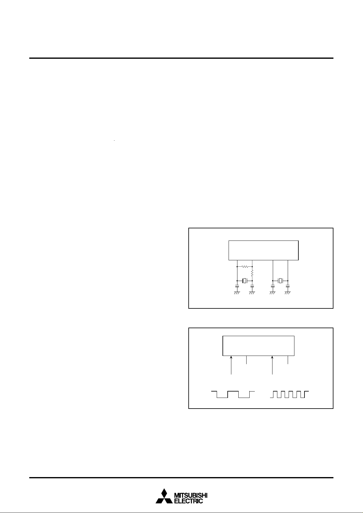
MITSUBISHI MICROCOMPUTERS
3819 Group
SINGLE-CHIP 8-BIT CMOS MICROCOMPUTER
CLOCK GENERATING CIRCUIT
The 3819 group has two built-in oscillation circuits. An oscillation
circuit can be formed by connecting a resonator between XIN and
XOUT (XCIN and XCOUT). Use the circuit constants in accordance
with the resonator manufacturer's recommended values. No external resistor is needed between XIN and XOUT since a feed-back
resistor exists on-chip. However, an external feed-back resistor is
needed between XCIN and XCOUT.
Immediately after poweron, only the XIN oscillation circuit starts
oscillation, and XCIN and XCOUT pins function as I/O ports.
Frequency Control
Middle-speed mode
The internal clock φ is the frequency of XIN divided by 8. After reset, this mode is selected.
High-speed mode
The internal clock φ is half the frequency of XIN.
Low-speed mode
The internal clock φ is half the frequency of XCIN.
Note : If you switch the mode between middle/high-speed and low-speed,
stabilize both X
quired for the X
after poweron and at returning from stop mode. When switching the
mode between middle/high-speed and low-speed, set the frequency
on condition that f(X
Low-power dissipation mode
When stopping the main clock XIN in the low-speed mode, the lowpower dissipation operation starts. To stop the main clock, set the
bit 5 of the CPU mode register to “1”. When the main clock XIN is
restarted, set enough time for oscillation to stabilize by programming.
The low-power dissipation operation 200 µA or less (at f(XIN) = 32
kHz) can be realized by reducing the XCIN–XCOUT drivability. To reduce the XCIN–XCOUT drivability, clear the bit 3 of the CPU mode
register to “0”. At reset or when executing the STP instruction, this
bit is set to “1” and strong drivability is selected to help the oscillation to start.
IN and XCIN oscillations. The sufficient time is re-
CIN oscillation to stabilize, especially immediately
IN) > 3·f(XCIN).
Oscillation Control
Stop mode
If the STP instruction is executed, the internal clock φ stops at an
“H” level, and XIN and XCIN oscillators stop. Timer 1 is set to “FF16”
and timer 2 is set to “0116”. Either XIN or XCIN divided by 16 is input to timer 1, and the output of timer 1 is connected to timer 2.
The bits of the timer 12 mode register are cleared to “0”. Set the
timer 1 and timer 2 interrupt enable bits to disabled (“0”) before executing the STP instruction.
Oscillator restarts at reset or when an external interrupt is received, but the internal clock φ is not supplied to the CPU until
timer 1 underflows. When using an external resonator, it is necessary for oscillating to stabilize.
Wait mode
If the WIT instruction is executed, the internal clock φ stops at an
“H” level. The states of XIN and XCIN are the same as the state before executing the WIT instruction. The internal clock restarts at
reset or when an interrupt is received. Since the oscillator does
not stop, normal operation can be started immediately after the
clock is restarted.
X
CINXCOUT
R
f
C
CIN
Fig. WA-1 Ceramic resonator external circuit
XINX
OUT
R
d
C
COUT
C
IN
C
OUT
X
CINXCOUT
Open Open
External oscillation
circuit or pulse
CC
V
V
SS
V
CC
V
SS
Fig. WA-2 External clock input circuit
XINX
OUT
External oscillation
circuit
47
Page 48

MITSUBISHI MICROCOMPUTERS
3819 Group
SINGLE-CHIP 8-BIT CMOS MICROCOMPUTER
X
CIN
X
COUT
“0”
“1”
Port XC switch bit (Note 3)
X
IN
QS
R STP instruction
Interrupt disable flag I
Interrupt request
Internal system clock selection bit
X
OUT
Low-speed mode
“1”
“1”
“0”
“0”
Middle/
High-speed mode
Main clock stop bit (Note 3)
Reset
(Note 1, 3)
1/41/2 1/2
High-speed mode
or Low-speed mode
WIT
instruction
Timer 1 count
source selection
bit (Note 2)
“1”
Timer 1
“0”
Main clock division ratio selection bit (Note 3)
Middle-speed mode
Timing φ
(Internal clock)
SQ
R
QS
R STP instruction
Notes
Fig. WA-3 Clock generating circuit block diagram
1 : When selecting the low-speed mode, set the port XC switch bit to “1”.
2 : Refer to the structure of timer 12 mode register.
3 : Refer to the structure of CPU mode register (next page).
48
Page 49

Reset
MITSUBISHI MICROCOMPUTERS
3819 Group
SINGLE-CHIP 8-BIT CMOS MICROCOMPUTER
Middle-speed mode (φ =1 MHz)
CM
7 = 0 (8 MHz selected)
CM
6 = 1 (Middle-speed)
5 = 0 (XIN oscillating)
CM
CM
4 = 0 (32 kHz stopped)
CM
CM4
“1” “0”
Middle-speed mode (φ =1 MHz)
CM
7 = 0 (8 MHz selected)
CM
6 = 1 (Middle-speed)
CM
5 = 0 (XIN oscillating)
4 = 1 (32 kHz oscillating)
CM
“1” “0”
CM7
“1” “0”
Low-speed mode (φ =16 kHz)
CM
7 = 1 (32 kHz selected)
6 = 1 (Middle-speed)
CM
CM
5 = 0 (XIN oscillating)
CM
4 = 1 (32 kHz oscillating)
4
6
CM
“1” “0”
CM6
“1” “0”
CM6
“1” “0”
CM6
“1” “0”
High-speed mode (φ = 4 MHz)
CM
7 = 0 (8 MHz selected)
CM
6 = 0 (High-speed)
5 = 0 (XIN oscillating)
CM
CM
4 = 0 (32 kHz stopped)
CM
“0” “1”
4
CM
“1” “0”
6
High-speed mode (φ = 4 MHz)
CM
7 = 0 (8 MHz selected)
CM
6 = 0 (High-speed)
CM
5 = 0 (XIN oscillating)
4 = 1 (32 kHz oscillating)
CM
Low-speed mode (φ = 16 kHz)
CM
7 = 1 (32 kHz selected)
6 = 0 (High-speed)
CM
CM
5 = 0 (XIN oscillating)
CM
4 = 1 (32 kHz oscillating)
CM4
“1” “0”
CM7
“1” “0”
b7
b0
CPU mode register
(CPUM (CM) : address 003B
16)
5
CM
CM5
“1” “0”
6
“1” “0”
CM
“1” “0”
Low power dissipation mode (φ =16 kHz)
7 = 1 (32 kHz selected)
CM
CM
6 = 1 (Middle-speed)
5 = 1 (XIN stopped)
CM
CM
4 = 1 (32 kHz oscillating)
Notes 1 :
Switch the mode by the allows shown between the mode blocks. (Do not switch between the mode directly without an allow.)
The all modes can be switched to the stop mode or the wait mode and return to the source mode when the stop mode or the wait mode
2 :
“1” “0”
is ended.
Timer operates in the wait mode.
When the stop mode is released in middle/high-speed mode, a delay of approximately 0.5 ms occurs automatically by timer 1.
3 :
When the stop mode is released in low-speed mode, a delay of approximately 0.125 s occurs automatically by timer 1.
4 :
The example assumes that 8 MHz is being applied to the X
5 :
Fig. WA-4 State transitions of system clock
CM
CM
“0” “1”
5
CM
“1” “0”
6
Low power dissipation mode (φ =16 kHz)
6
CM
CM
CM
CM
CM5
“1” “0”
7 = 1 (32 kHz selected)
6 = 0 (High-speed)
5 = 1 (XIN stopped)
4 = 1 (32 kHz oscillating)
IN pin and 32 kHz to the XCIN pin. φ indicates the internal clock.
CM
4 : Port XC switch bit
0 : I/O port function
1 : X
CIN-XCOUT oscillating function
5 : Main clock (XIN-XOUT) stop bit
CM
0 : Oscillating
1 : Stopped
CM
6 : Main clock division ratio selection bit
IN)/2 (high-speed mode)
0 : f(X
1 : f(X
IN)/8 (middle-speed mode)
CM
7 : Internal system clock selection bit
0 : X
IN-XOUT selected
(middle/high-speed mode)
1 : X
CIN-XCOUT selected
(low-speed mode)
49
Page 50

MITSUBISHI MICROCOMPUTERS
3819 Group
SINGLE-CHIP 8-BIT CMOS MICROCOMPUTER
NOTES ON PROGRAMMING
Processor Status Register
The contents of the processor status register (PS) after a reset are
undefined, except for the interrupt disable flag (I) which is “1”. After a reset, initialize flags which affect program execution. In
particular, it is essential to initialize the index X mode (T) and the
decimal mode (D) flags because of their effect on calculations.
Interrupts
The contents of the interrupt request bits do not change immediately after they have been written. After writing to an interrupt
request register, execute at least one instruction before performing
a BBC or BBS instruction.
Decimal Calculations
• To calculate in decimal notation, set the decimal mode flag (D)
to “1”, then execute an ADC or SBC instruction. Only the ADC
and SBC instructions yield proper decimal results. After executing an ADC or SBC instruction, execute at least one instruction
before executing a SEC, CLC, or CLD instruction.
• In decimal mode, the values of the negative (N), overflow (V),
and zero (Z) flag are invalid.
The carry flag can be used to indicate whether a carry or borrow
has occurred. Initialize the carry flag before each calculation.
Clear the carry flag before an ADC and set the flag before an
SBC.
Timers
If a value n (between 0 and 255) is written to a timer latch, the frequency division ratio is 1/(n+1).
Serial I/O
When using an external clock, input “H” to the external clock input
pin and clear the serial I/O interrupt request bit before executing
serial I/O transfer and serial I/O automatic transfer.
When using the internal clock, set the synchronous clock to internal clock, then clear the serial I/O interrupt request bit before
executing a serial I/O transfer and serial I/O automatic transfer.
A-D Converter
The comparator uses internal capacitors whose charge will be lost
if the clock frequency is too low.
Make sure that f(XIN) is 500 kHz or more during an A-D conversion.
Do not execute the STP or WIT instruction during an A-D conversion.
Instruction Execution Time
The instruction execution time is obtained by multiplying the frequency of the internal clock φ by the number of cycles needed to
execute an instruction.
The number of cycles required to execute an instruction is shown
in the list of machine instructions. The frequency of the internal
clock φ is half of the XIN or XCIN frequency.
At the STP Instruction Release
At the STP instruction release, all bits of the timer 12 mode register are cleared.
The XCOUT drivability selection bit (the CPU mode register) is set
to “1” (high drive) in order to start oscillating.
Multiplication and Division Instructions
• The index X mode (T) and the decimal mode (D) flags do not affect the MUL and DIV instruction.
• The execution of these instructions does not change the contents of the processor status register.
Ports
The contents of the port direction registers cannot be read. The
following cannot be used:
• the data transfer instruction (LDA, etc.)
• the operation instruction when the index X mode flag (T) is “1”
• the addressing mode which uses the value of a direction register
as an index
• the bit-test instruction (BBC or BBS, etc.) to a direction register
• the read-modify-write instructions (ROR, CLB, or SEB, etc.) to a
direction register.
Use instructions such as LDM and STA, etc., to set the port direction registers.
50
Page 51

MITSUBISHI MICROCOMPUTERS
3819 Group
SINGLE-CHIP 8-BIT CMOS MICROCOMPUTER
DATA REQUIRED FOR MASK ORDERS
The following are necessary when ordering a mask ROM production:
(1) Mask ROM Order Confirmation Form
(2) Mark Specification Form
(3) Data to be written to ROM, in EPROM form (three identical
copies)
PROM PROGRAMMING METHOD
The built-in PROM of the blank One Time PROM version and builtin EPROM version can be read or programmed with a generalpurpose PROM programmer using a special programming
adapter.
Package
100P6S-A
100D0
Set the address of PROM programmer in the user ROM area.
The PROM of the blank One Time PROM version is not tested or
screened in the assembly process and following processes. To ensure proper operation after writing, the procedure shown in Figure
XC-1 is recommended to verify programming.
Name of Programming Adapter
PCA4738F-100A
PCA4738L-100A
Programming with
PROM Programmer
Screening (Caution)
(150°C for 40 hours)
Verification with
PROM Programmer
Functional check in target device
Caution :
Fig. XC-1 Programming and testing of One Time PROM version
The screening temperature is far higher than
the storage temperature. Never expose to
150°C exceeding 100 hours.
51
Page 52

MITSUBISHI MICROCOMPUTERS
3819 Group
SINGLE-CHIP 8-BIT CMOS MICROCOMPUTER
ABSOLUTE MAXIMUM RATINGS
Symbol Ratings Unit
VCC
VEE
VI
VI
VI
VI
VI
VO
VO
Pd
Topr
Tstg
Power source voltage
Pull-down power source voltage
Input voltage P24–P27, P41–P44, P46, P47,
Input voltage P40, P45
Input voltage P80–P87, PA0–PA7
Input voltage RESET, XIN
Input voltage XCIN
Output voltage P00–P07, P10–P17, P20–P23,
Output voltage P24–P27, P41–P44, P46, P47, P50–P57,
Power dissipation
Operating temperature
Storage temperature
Parameter
P50–P57, P60–P67, P70–P77, PB0–PB3
All voltages are based on VSS.
Output transistors are cut off.
P30–P37, P80–P87, P90–P97, PA0–PA7
P60–P67, P70–P77, PB0–PB3, XOUT,
XCOUT
Ta = 25°C
Conditions
–0.3 to 7.0
VCC –40 to V
–0.3 to VCC +0.3
–0.3 to VCC +0.3
VCC –40 to V
–0.3 to VCC +0.3
–0.3 to VCC +0.3
VCC –40 to V
–0.3
CC
CC
CC
to V
CC
600
–10 to 85
–40 to 125
+
+0.3
+0.3
+0.3
0.3
V
V
V
V
V
V
V
V
V
mW
°C
°C
RECOMMENDED OPERATING CONDITIONS (Vcc = 4.0 to 5.5 V, Ta = –10 to 85°C, unless otherwise noted)
Symbol
VCC
VSS
VEE
VREF
AVSS
VIA
VIH
VIH
VIH
VIH
VIH
VIL
VIL
VIL
VIL
VIL
Parameter
Power source voltage
Power source voltage
Pull-down power source voltage
Analog reference voltage (when using A-D converter)
Analog reference voltage (when using D-A converter)
Analog power source voltage
Analog input voltage AN0–AN15
“H” input voltage P40–P47, P50–P57, P60–P67,
“H” input voltage P24–P27
“H” input voltage P80–P87, PA0–PA7
“H” input voltage RESET
“H” input voltage XIN, XCIN
“L” input voltage P40–P47, P50–P57, P60–P67,
“L” input voltage P24–P27
“L” input voltage P80–P87, PA0–PA7
“L” input voltage RESET
“L” input voltage XIN, XCIN
High-speed mode
Middle/Low-speed mode
P70–P77, PB0–PB3
P70–P77, PB0–PB3
Min.
4.0
2.8
VCC–38
2.0
3.0
0
0.75VCC
0.4VCC
0.8VCC
0.8VCC
0.8VCC
0
0
0
0
0
Limits
Typ.
5.0
5.0
0
0
Max.
5.5
5.5
VCC
VCC
VCC
VCC
VCC
VCC
VCC
VCC
VCC
0.25VCC
0.16VCC
0.2VCC
0.2VCC
0.2VCC
Unit
V
V
V
V
V
V
V
V
V
V
V
V
V
V
V
V
V
V
52
Page 53

MITSUBISHI MICROCOMPUTERS
3819 Group
SINGLE-CHIP 8-BIT CMOS MICROCOMPUTER
RECOMMENDED OPERATING CONDITIONS (Vcc = 4.0 to 5.5 V, Ta = –10 to 85°C, unless otherwise noted)
Symbol
“H” total peak output current P00–P07, P10–P17, P20–P27,
ΣIOH(peak)
ΣIOL(peak)
ΣIOH(avg)
ΣIOL(avg)
IOH(peak)
IOH(peak)
IOL(peak)
IOH(avg)
IOH(avg)
IOL(avg)
f(CNTR0)
f(CNTR1)
f(XIN)
f(XCIN)
Notes 1: The total output current is the sum of all the currents flowing through all the applicable ports.The total average
“H” total peak output current P4 1–P44, P46, P47, P50–P57 ,
“L” total peak output current P24–P27, P41–P44, P46, P47,
“H” total average output current P00–P07, P10–P17, P20–P27,
“H” total average output current P41–P44, P46, P47, P50–P57,
“L” total average output current P24–P27, P41–P44, P46, P47,
“H” peak output current P00–P07, P10–P17, P20–P23,
“H” peak output current P24–P27, P41–P44, P46, P47,
“L” peak output current P24–P27, P41–P44, P46, P47,
“H” average output current P00–P07, P10–P17, P20–P23,
“H” average output current P24–P27, P41–P44, P46, P47,
“L” average output current P24–P27, P41–P44, P46, P47,
Clock input frequency for timers 2 and 4
(duty cycle 50%)
Main clock input oscillation frequency (Note 4)
Sub-clock input oscillation frequency (Note 4, 5)
current is an average value measured over 100 ms. The total peak current is the peak value of all the currents.
2: The peak output current is the peak current flowing in each port.
3: The average output current in an average value measured over 100 ms.
4: When the oscillation frequency has a 50% duty cycle.
5: When using the microcomputer in low-speed operation mode, set the sub-clock input oscillation frequency on
condition that f(X
CIN) < f(XIN)/3.
Parameter Unit
P30–P37, P80–P87, P90–P97,
(Note 1) PA6, PA7
P60–P67, P70–P77, PA0–PA5,
(Note 1) PB0–PB3
P50–P57, P60–P67, P70–P77,
(Note 1) PB0–PB3
P30–P37, P80–P87, P90–P97,
(Note 1) PA6, PA7
P60–P67, P70–P77, PA0–PA5,
(Note 1) PB0–PB3
P50–P57, P60–P67, P70–P77,
(Note 1) PB0–PB3
P30–P37, P80–P87, P90–P97,
(Note 2) PA0–PA7
P50–P57, P60–P67, P70–P77,
(Note 2) PB0–PB3
P50–P57, P60–P67, P70–P77,
(Note 3) PB0–PB3
P30–P37, P80–P87, P90–P97,
(Note 3) PA0–PA7
P50–P57, P60–P67, P70–P77,
(Note 3) PB0–PB3
P50–P57, P60–P67, P70–P77,
(Note 3) PB0–PB3
Min.
Limits
Typ. Max.
32.768
–240
–60
100
–120
–30
50
–40
–10
10
–18
–5.0
5.0
250
8.4
50
mA
mA
mA
mA
mA
mA
mA
mA
mA
mA
mA
mA
kHz
MHz
kHz
53
Page 54

MITSUBISHI MICROCOMPUTERS
SINGLE-CHIP 8-BIT CMOS MICROCOMPUTER
ELECTRICAL CHARACTERISTICS (Vcc = 4.0 to 5.5 V, Ta = –10 to 85°C, unless otherwise noted)
Symbol Parameter
“H” output voltage P00–P07, P10–P17, P20–P23,
VOH
“H” output voltage P24–P27, P41–P44, P46, P47,
VOH
“L” output voltage P24–P27, P41–P44, P46, P47,
VOL
VT+–VT–
VT+–VT–
VT+–VT–
IH
IH
IH
IH
IL
IL
IL
IL
ILOAD
ILEAK
VRAM
Note : Except when reading ports P8 or PA.
Hysteresis INT0–INT4, SIN1, SIN2, SIN3, SCLK11,
Hysteresis RESET, XIN
Hysteresis XCIN
“H” input current P24–P27, P40–P47, P50–P57,
“H” input current P80–P87, PA0–PA7 (Note)
“H” input current RESET, XCIN
“H” input current XIN
“L” input current P24–P27, P40–P47, P50–P57,
“L” input current P80–P87, PA0–PA7 (Note)
“L” input current RESET , XCIN
“L” input current XIN
Output load current P00–P07, P10–P17, P20–P23,
Output leakage current P00–P07, P10–P17,
RAM hold voltage
P30–P37, P80–P87, P90–P97,
PA0–PA7
P50–P57, P60–P67, P70–P77,
PB0–PB3
P50–P57, P60–P67, P70–P77,
PB0–PB3
SCLK2, SCLK3, CS, CNTR0, CNTR1
P60–P67, P70–P77, PB0–PB3
P60–P67, P70–P77, PB0–PB3
P30–P37, P90–P97
P20–P23, P30–P37,
P80–P87, P90–P97,
PA0–PA7
Test conditions
IOH=–18 mA
IOH=–10 mA
IOL=10 mA
When using a non-port
function
VI=VCC
VI=VCC
VI=VCC
VI=VCC
VI=VSS
VI=VSS
VI=VSS
VI=VSS
VEE=VCC–36 V , VOL=VCC,
Output transistors “off”
VEE=VCC–38 V ,
VOL=VCC–38 V ,
Output transistors “off”
When clock is stopped
Min.
VCC–2.0
VCC–2.0
150
2
Limits
Typ.
–4.0
500
3819 Group
Max.
2.0
0.4
0.5
0.5
5.0
5.0
5.0
4.0
–5.0
–5.0
–5.0
900
–10
5.5
Unit
V
V
V
V
V
V
µA
µA
µA
µA
µA
µA
µA
µA
µA
µA
V
54
Page 55

MITSUBISHI MICROCOMPUTERS
SINGLE-CHIP 8-BIT CMOS MICROCOMPUTER
ELECTRICAL CHARACTERISTICS (VCC = 4.0 to 5.5 V, Ta = –10 to 85°C, unless otherwise noted)
Symbol Test conditions
ICC
Power source current
Parameter
• High-speed mode
f(XIN) = 8.4 MHz
f(XCIN) = 32 kHz
Output transistors “off”
• High-speed mode
f(XIN) = 8.4 MHz (in WIT state)
f(XCIN) = 32 kHz
Output transistors “off”
• Middle-speed mode
f(XIN) = 8.4 MHz
f(XCIN) = stopped
Output transistors “off”
• Middle-speed mode
f(XIN) = 8.4 MHz (in WIT state)
f(XCIN) = stopped
Output transistors “off”
• Low-speed mode
f(XIN) = stopped, f(XCIN) = 32 kHz
Low-power dissipation mode set
(CM3) = 0
Output transistors “off”
• Low-speed mode
f(XIN) = stopped
f(XCIN) = 32 kHz
Low-power dissipation mode set
(CM3) = 0
Output transistors “off”
Increase at A-D converter operating
f(XIN) = 8.4 MHz
Increase at zero cross detection
(P45 = VCC)
All oscillation stopped
(in STP state)
Output transistors “off”
(in WIT state)
Ta = 25°C
Ta = 85°C
Min. Typ.
3819 Group
Limits
Max.
7.5
1
3
1
60
20
0.6
1
0.1
15
200
40
1
10
Unit
mA
mA
mA
mA
µA
µA
mA
mA
µA
55
Page 56

ZERO CROSS DETECTION INPUT CHARACTERISTICS
(VCC = 4.0 to 5.5 V, VSS = 0 V, Ta = –10 to 85°C, unless otherwise noted)
Symbol
fZCR
∆VT
Input frequency of zero cross detection
Voltage error of zero cross detection distinction
Parameter
50 Hz or 60 Hz
1/fZCR
100V AC
MITSUBISHI MICROCOMPUTERS
3819 Group
SINGLE-CHIP 8-BIT CMOS MICROCOMPUTER
Test conditions
Min.
–100
Limits
Typ.
50, 60
0
Max.
1000
100
Unit
Hz
mV
P45/INT1/ZCR
clamp correction
input waveform
Zero cross detection
comparator output
Fig. ZA-1 Zero cross detection input characteristics
A-D CONVERTER CHARACTERISTICS
(VCC = 4.0 to 5.5 V, VSS = 0 V, Ta = –10 to 85°C, high-speed operation mode f(XIN) = 500 kHz to 8.4 MHz, unless otherwise noted)
Symbol
–
–
TCONV
IVREF
IIA
RLADDER
Resolution
Absolute accuracy (excluding quantization error)
Conversion time
Reference power source input current
Analog port input current
Ladder resistor
Parameter
Test conditions
VCC = VREF = 5.12 V
VREF = 5 V
5.7 V
V
I
VT
0 V
– 0.7 V
Min.
49
50
Limits
Typ.
±1
150
0.5
35
Max.
±2.5
50
200
5.0
Unit
Bits
8
LSB
tc (φ)
µA
µA
kΩ
D-A CONVERTER CHARACTERISTICS
(VCC = 4.0 to 5.5 V, VSS = AVSS = 0 V, VREF = 3.0 to VCC, Ta = –10 to 85°C, unless otherwise noted)
Symbol
–
–
Tsu
RO
IVREF
Note : Exclude currents flowing through the A-D converter ladder resistor
56
Resolution
Absolute accuracy
Setting time
Output resistor
Reference power source input current (Note)
Parameter
VCC = 4.0 to 5.5 V
VCC = 3.0 to 5.5 V
Test conditions
Min.
1
Limits
Typ.
2.5
Max.
8
1.0
2.5
3
4
3.2
Unit
Bits
%
%
µs
kΩ
mA
Page 57

MITSUBISHI MICROCOMPUTERS
SINGLE-CHIP 8-BIT CMOS MICROCOMPUTER
TIMING REQUIREMENTS (VCC = 4.0 to 5.5 V, VSS = 0 V, Ta = –10 to 85°C, unless otherwise noted)
Symbol
tW(RESET)
tC(XIN)
tWH(XIN)
tWL(XIN)
tC(XcIN)
tWH(XcIN)
tWL(XcIN)
tC(CNTR)
tWH(CNTR)
tWL(CNTR)
tWH(INT)
tWL(INT)
tC(SCLK)
tWH(SCLK)
tWL(SCLK)
tsu(SCLK–SIN)
th(SCLK–SIN)
Reset input “L” pulse width
Main clock input cycle time (XIN input)
Main clock input “H” pulse width
Main clock input “L” pulse width
Sub-clock input cycle time (XCIN input)
Sub-clock input “H” pulse width
Sub-clock input “L” pulse width
CNTR0, CNTR1 input cycle time
CNTR0, CNTR1 input “H” pulse width
CNTR0, CNTR1 input “L” pulse width
INT0–INT4 input “H” pulse width
INT0–INT4 input “L” pulse width
Serial I/O clock input cycle time
Serial I/O clock input “H” pulse width
Serial I/O clock input “L” pulse width
Serial I/O input setup time
Serial I/O input hold time
Parameter
Min.
2.0
119
30
30
20
5.0
5.0
4.0
1.6
1.6
80
80
1.0
400
400
200
200
3819 Group
Limits
Typ. Max.
Unit
µs
ns
ns
ns
µs
µs
µs
µs
µs
µs
ns
ns
µs
ns
ns
ns
ns
SWITCHING CHARACTERISTICS (VCC = 4.0 to 5.5 V, VSS = 0 V, Ta = –10 to 85°C, unless otherwise noted)
Symbol
tWH(SCLK)
tWL(SCLK)
td(SCLK–SOUT)
tv(SCLK–SOUT)
tr(SCLK)
tf(SCLK)
tr(Pch–strg)
tf(Pch–weak)
Notes 1: When the bit 7 of the FLDC mode register 1 (address 003616) is at “0”.
2: When the bit 7 of the FLDC mode register 1 (address 0036
Serial clock output port
Serial I/O clock output “H” pulse width
Serial I/O clock output “L” pulse width
Serial I/O output delay time
Serial I/O output hold time
Serial I/O clock output rising time
Serial I/O clock output falling time
High-breakdown-voltage P-channel opendrain output rising time (Note 1)
High-breakdown-voltage P-channel opendrain output falling time (Note 2)
Parameter
P56/S
CLK3
P52/S
CLK2
6/SCLK11
P6
CL = 100 pF
CL = 100 pF
CL = 100 pF
CL = 100 pF
CL = 100 pF
VEE = VCC –36 V
CL = 100 pF
VEE = VCC –36 V
16) is at “1”.
,
,
L
C
Test conditions
High-breakdown-voltage
P-channel open-drain
output port
Min.
tc(SCLK)
/2–160
tc(SCLK)
/2–160
Limits
Typ.
0
55
1.8
P0, P1, P20–P23,
P3, P8, P9, PA
0.2t
Max.
c(S
40
40
Unit
ns
ns
ns
CLK
)
ns
ns
ns
ns
µs
C
L
Note : Ports P8 and PA need external resistors.
Fig. ZA-2 Circuit for measuring output switching characteristics
(Note)
V
EE
57
Page 58

TIMING DIAGRAM
CNTR
0
CNTR
1
INT0-
4
INT
0.8V
0.8V
MITSUBISHI MICROCOMPUTERS
3819 Group
SINGLE-CHIP 8-BIT CMOS MICROCOMPUTER
t
C(CNTR)
t
t
WH(CNTR)
CC
0.2V
t
WH(INT)
CC
0.2V
WL(CNTR)
CC
t
WL(INT)
CC
RESET
X
X
CIN
S
CLK
t
W(RESET)
0.8V
t
WL(XIN)
t
WL(X
t
WH(S
CC
CIN
)
CLK
)
0.2V
CC
t
C(XIN)
t
WH(XIN)
0.8V
IN
CC
t
WH(X
CIN
)
0.8V
CC
t
f
0.2V
t
WL(S
CLK
)
CC
0.2V
CC
t
C(X
CIN
)
0.2V
CC
t
C(S
CLK
)
t
r
0.8V
CC
58
t
h(S
CLK
-
t
su(S
IN
-
S
CLK
)
0.8V
S
IN
t
d(S
CLK
-
S
OUT
)
S
OUT
0.2V
CC
CC
SIN)
t
v(S
CLK
-
S
OUT
)
Page 59

MITSUBISHI MICROCOMPUTERS
3819 Group
SINGLE-CHIP 8-BIT CMOS MICROCOMPUTER
Keep safety first in your circuit designs!
• Mitsubishi Electric Corporation puts the maximum effort into making semiconductor products better and more reliable, but there is always the possibility that trouble may occur with them. Trouble with
semiconductors may lead to personal injury, fire or property damage. Remember to give due consideration to safety when making your circuit designs, with appropriate measures such as (i) placement of
substitutive, auxiliary circuits, (ii) use of non-flammable material or (iii) prevention against any malfunction or mishap.
Notes regarding these materials
• These materials are intended as a reference to assist our customers in the selection of the Mitsubishi semiconductor product best suited to the customer’s application; they do not convey any license under any
intellectual property rights, or any other rights, belonging to Mitsubishi Electric Corporation or a third party.
• Mitsubishi Electric Corporation assumes no responsibility for any damage, or infringement of any third-party’s rights, originating in the use of any product data, diagrams, charts or circuit application examples
contained in these materials.
• All information contained in these materials, including product data, diagrams and charts, represent information on products at the time of publication of these materials, and are subject to change by Mitsubishi
Electric Corporation without notice due to product improvements or other reasons. It is therefore recommended that customers contact Mitsubishi Electric Corporation or an authorized Mitsubishi Semiconductor
product distributor for the latest product information before purchasing a product listed herein.
• Mitsubishi Electric Corporation semiconductors are not designed or manufactured for use in a device or system that is used under circumstances in which human life is potentially at stake. Please contact
Mitsubishi Electric Corporation or an authorized Mitsubishi Semiconductor product distributor when considering the use of a product contained herein for any specific purposes, such as apparatus or systems for
transportation, vehicular, medical, aerospace, nuclear, or undersea repeater use.
• The prior written approval of Mitsubishi Electric Corporation is necessary to reprint or reproduce in whole or in part these materials.
• If these products or technologies are subject to the Japanese export control restrictions, they must be exported under a license from the Japanese government and cannot be imported into a country other than the
approved destination.
Any diversion or reexport contrary to the export control laws and regulations of Japan and/or the country of destination is prohibited.
• Please contact Mitsubishi Electric Corporation or an authorized Mitsubishi Semiconductor product distributor for further details on these materials or the products contained therein.
© 1998 MITSUBISHI ELECTRIC CORP.
New publication, effective Jan. 1998.
Specifications subject to change without notice.
Page 60

REVISION DESCRIPTION LIST 3819 GROUP DATA SHEET
Rev. Rev.
No. date
1.0 First Edition 980109
Revision Description
(1/1)
 Loading...