

Page 1

Mitsubishi 32-bit RISC Single-chip Microcomputers
M32R Family M32R/ECU Series
32172
32173
Group
User’s Manual
http://www.infomicom.maec.co.jp/indexe.htm
Before using this material, please visit the above website to confirm that this is
the most current document available.
Revision date: Oct. 5, 2001
Rev. 1.0
Page 2

Keep safety first in your circuit designs!
•
Mitsubishi Electric Corporation puts the maximum effort into making semiconductor products better and more reliable, but there is always the possibility that trouble may occur with
them. Trouble with semiconductors may lead to personal injury, fire or property damage.
Remember to give due consideration to safety when making your circuit designs, with appropriate measures such as (i) placement of substitutive, auxiliary circuits, (ii) use of nonflammable material or (iii) prevention against any malfunction or mishap.
Notes regarding these materials
•
These materials are intended as a reference to assist our customers in the selection of the
Mitsubishi semiconductor product best suited to the customer's application; they do not
convey any license under any intellectual property rights, or any other rights, belonging to
Mitsubishi Electric Corporation or a third party.
•
Mitsubishi Electric Corporation assumes no responsibility for any damage, or infringement
of any third-party's rights, originating in the use of any product data, diagrams, charts,
programs, algorithms, or circuit application examples contained in these materials.
•
All information contained in these materials, including product data, diagrams, charts, programs and algorithms represents information on products at the time of publication of these
materials, and are subject to change by Mitsubishi Electric Corporation without notice due
to product improvements or other reasons. It is therefore recommended that customers
contact Mitsubishi Electric Corporation or an authorized Mitsubishi Semiconductor product
distributor for the latest product information before purchasing a product listed herein.
The information described here may contain technical inaccuracies or typographical errors.
Mitsubishi Electric Corporation assumes no responsibility for any damage, liability , or other
loss rising from these inaccuracies or errors.
Please also pay attention to information published by Mitsubishi Electric Corporation by
various means, including the Mitsubishi Semiconductor home page (http://
www.mitsubishichips.com).
•
When using any or all of the information contained in these materials, including product
data, diagrams, charts, programs, and algorithms, please be sure to evaluate all information as a total system before making a final decision on the applicability of the information
and products. Mitsubishi Electric Corporation assumes no responsibility for any damage,
liability or other loss resulting from the information contained herein.
•
Mitsubishi Electric Corporation semiconductors are not designed or manufactured for use
in a device or system that is used under circumstances in which human life is potentially at
stake. Please contact Mitsubishi Electric Corporation or an authorized Mitsubishi Semiconductor product distributor when considering the use of a product contained herein for any
specific purposes, such as apparatus or systems for transportation, vehicular, medical,
aerospace, nuclear, or undersea repeater use.
•
The prior written approval of Mitsubishi Electric Corporation is necessary to reprint or reproduce in whole or in part these materials.
•
If these products or technologies are subject to the Japanese export control restrictions,
they must be exported under a license from the Japanese government and cannot be imported into a country other than the approved destination.
Any diversion or reexport contrary to the export control laws and regulations of Japan and/
or the country of destination is prohibited.
•
Please contact Mitsubishi Electric Corporation or an authorized Mitsubishi Semiconductor
product distributor for further details on these materials or the products contained therein.
Page 3
REVISION HISTORY 32172/32173 GROUP USER’S MANUAL
Rev. Date Description
Page Summary
1.0 10/5/2001 - First edition issued
Page 4
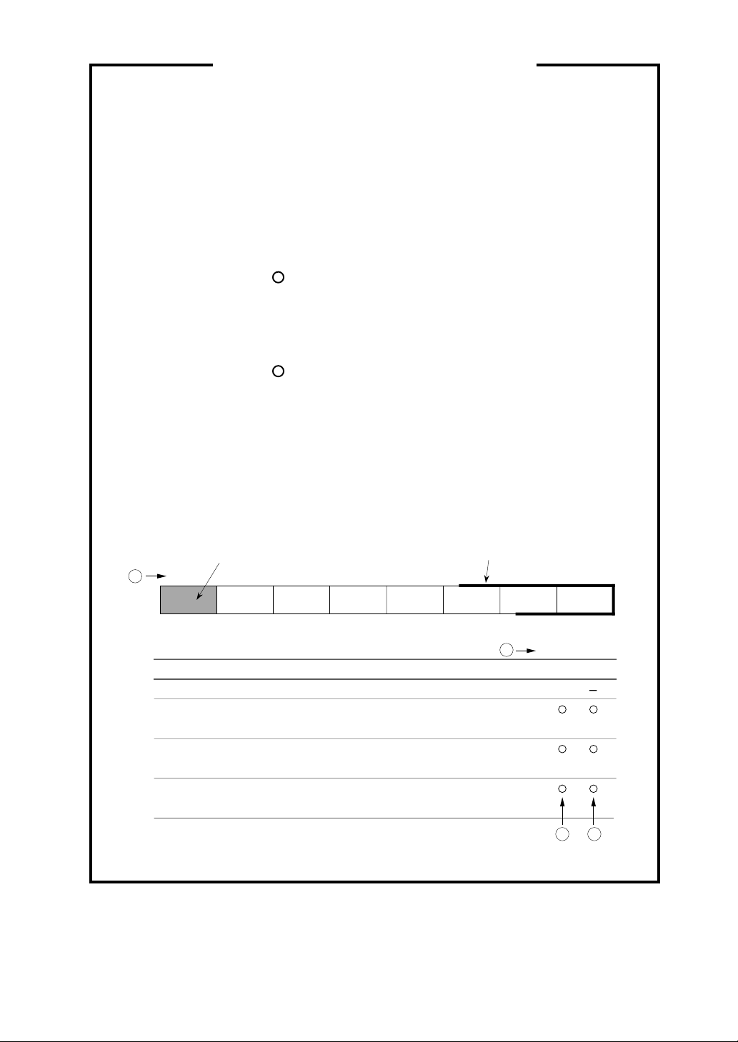
How to read internal I/O register tables
➀ Bit Numbers: Each register is connected with an internal bus of 16-bit
wide, so the bit numbers of the registers located at even
addresses are D0-D7, and those at odd addresses are
D8-D15.
➁ State of Register at Reset: Represents the initial state of each register
immediately after reset with hexadecimal numbers
(undefined bits after reset are indicated each in column ➂.)
➂ At read: ... read enabled
? ... read disabled (read value invalid)
0 ... Read always as 0
1 ... Read always as 1
④ At write: : Write enabled
∆ : Write enable conditionally
(include some conditions at write)
- : Write disabled (Written value invalid)
<Example of representation>
Not implemented
in the shaded portion.
1
D
0 Not assigned.
1 Abit
2
3
Bit name Function
(...................)
Bbit
(...................)
Cbit
(...................)
1234D0
Abit
Bbit Cbit
0: ----1: -----
0: ----1: -----
0: ----1: ----
Registers represented with thick rectangles
are accessible only with halfwords or words
(not accessible with bytes)
-
2
.
<at reset: H'04>
WR
0
3 4
Page 5

CONTENTS
CHAPTER 1 OVERVIEW
1.1 Overview................................................................................................................ 1-2
1.1.1 M32R Family CPU Core.....................................................................1-2
1.1.2 Built-in Multiply-Accumulate Operation Function................................ 1-3
1.1.3 Built-in Flash Memory and RAM......................................................... 1-3
1.1.4 Built-in Clock Multiplier Circuit............................................................1-4
1.1.5 Built-in Powerful Peripheral Functions ...............................................1-4
1.1.6 Built-in Full-CAN Function .................................................................. 1-5
1.1.7 Two Built-in D-A Converters...............................................................1-5
1.1.8 Built-in Timer/Arithmetic Circuits for PD (Phase Digital) Sensors ......1-6
1.1.9 Built-in Debug Function ...................................................................... 1-6
1.2 Block Diagram ........................................................................................................ 1-7
1.3 Pin Functions .......................................................................................................... 1-10
1.4 Pin Layout............................................................................................................... 1-18
CHAPTER 2 CPU
2.1 CPU Registers ....................................................................................................... 2-2
2.2 General-purpose Registers.................................................................................... 2-2
2.3 Control Registers ................................................................................................... 2-3
2.3.1 Processor Status Word Register: PSW (CR0) .........................................2-4
2.3.2 Condition Bit Register: CBR (CR1) ..........................................................2-5
2.3.3 Interrupt Stack Pointer: SPI (CR2) ...........................................................2-5
User Stack Pointer: SPU (CR3)
2.3.4 Backup PC: BPC (CR6) ...........................................................................2-5
2.4 Accumulator........................................................................................................... 2-6
2.5 Program Counter ................................................................................................... 2-6
(1)
Page 6

2.6 Data Formats ......................................................................................................... 2-7
2.6.1 Data Types ...............................................................................................2-7
2.6.2 Data Formats............................................................................................2-8
CHAPTER 3 ADDRESS SPACE
3.1 Outline of the Address Space ................................................................................. 3-2
3.2 Operation Modes .................................................................................................... 3-5
3.3 Internal ROM and External Extended Areas........................................................... 3-8
3.3.1 Internal ROM Area .............................................................................. 3-8
3.3.2 External Extended Area ...................................................................... 3-8
3.4 Internal RAM and SFR Areas ................................................................................. 3-9
3.4.1 Internal RAM Area...............................................................................3-9
3.4.2 SFR (Special Function Register) Area ................................................3-9
3.5 EIT Vector Entry ..................................................................................................... 3-35
3.6 ICU Vector Table .................................................................................................... 3-36
3.7 Precautions on Address Space .............................................................................. 3-38
CHAPTER 4 EIT
4.1 Outline of EIT.......................................................................................................... 4-2
4.2 EIT Events .............................................................................................................. 4-3
4.2.1 Exceptions...........................................................................................4-3
4.2.2 Interrupts .............................................................................................4-3
4.2.3 Trap ..................................................................................................... 4-3
4.3 EIT Processing Procedure...................................................................................... 4-4
4.4 EIT Processing Mechanism .................................................................................... 4-6
4.5 Accepting EIT Events ............................................................................................. 4-7
4.6 Saving and Restoring PC and PSW ....................................................................... 4-8
4.7 EIT Vector Entry ..................................................................................................... 4-10
4.8 Exception Handling................................................................................................. 4-11
4.8.1 Reserved Instruction Exception (RIE) .................................................4-11
4.8.2 Address Exception (AE) ......................................................................4-13
(2)
Page 7

4.9 Interrupt Handling ................................................................................................... 4-15
4.9.1 Reset Interrupt (RI).............................................................................. 4-15
4.9.2 System Break Interrupt (SBI) .............................................................. 4-16
4.9.3 External Interrupt (EI) .......................................................................... 4-18
4.10 Trap Handling ....................................................................................................... 4-20
4.10.1 Trap (TRAP) ...................................................................................... 4-20
4.11 EIT Priority ............................................................................................................ 4-22
4.12 Example of EIT Processing .................................................................................. 4-23
4.13 Precautions on EIT ............................................................................................... 4-25
CHAPTER 5 INTERRUPT CONTROLLER (ICU)
5.1 Outline of the Interrupt Controller (ICU).................................................................. 5-2
5.2 Interrupt Sources of Internal Peripheral I/Os .......................................................... 5-4
5.3 ICU Related Registers ............................................................................................ 5-6
5.3.1 Interrupt Vector Register ....................................................................5-7
5.3.2 Interrupt Mask Register ...................................................................... 5-8
5.3.3 SBI (System Break Interrupt) Control Register .................................. 5-9
5.3.4 Interrupt Control Registers .................................................................5-10
5.4 ICU Vector Table .................................................................................................... 5-14
5.5 Description of Interrupt Operation........................................................................... 5-17
5.5.1 Accepting Interrupts from Internal Peripheral I/O ............................... 5-17
5.5.2 Processing of Internal Peripheral I/O Interrupts by Handler...............5-20
5.6 Description of System Break Interrupt (SBI) Operation .......................................... 5-22
5.6.1 Accepting SBI Interrupt ......................................................................5-22
5.6.2 SBI Processing by Handler ................................................................5-22
CHAPTER 6 INTERNAL MEMORY
6.1 Outline of the Internal Memory .............................................................................. 6-2
6.2 Internal RAM.......................................................................................................... 6-2
6.3 Internal Flash Memory ........................................................................................... 6-2
6.4 Internal Flash Memory Related Registers ............................................................. 6-3
(3)
Page 8

6.4.1 Flash Mode Register ..........................................................................6-4
6.4.2 Flash Status Registers .......................................................................6-5
6.4.3 Flash Control Registers......................................................................6-8
6.4.4 Virtual-flash L Bank Registers ............................................................ 6-14
6.4.5 Virtual-flash S Bank Registers............................................................ 6-15
6.5 Programming the Internal Flash Memory .............................................................. 6-16
6.5.1 Outline of Flash Memory Programming.............................................. 6-16
6.5.2 Controlling Operation Modes during Flash Programming ...................6-22
6.5.3 Procedure for Programming the Internal Flash Memory ....................6-25
6.5.4 Flash Programming Time (Reference Data) ...................................... 6-36
6.6 Boot ROM .............................................................................................................. 6-37
6.7 Virtual-flash Emulation Function ............................................................................ 6-38
6.7.1 Virtual-Flash Emulation Areas............................................................6-40
6.7.2 Transition to Virtual-Flash Emulation Mode ....................................... 6-45
6.7.3 Application Example for Virtual-Flash Emulation Mode ..................... 6-46
6.8 Connecting a Serial Programmer .......................................................................... 6-48
6.9 Precautions on Rewriting Flash Memory ............................................................... 6-50
CHAPTER 7 RESET
7.1 Outline of Reset ..................................................................................................... 7-2
7.2 Reset Operation..................................................................................................... 7-2
7.2.1 Power-on Reset.................................................................................. 7-2
7.2.2 Reset during Operation ......................................................................7-2
7.2.3 Reset Vector Movement during Flash Rewrite...................................7-2
7.3 Internal State Immediately after Reset .................................................................. 7-3
7.4 Precautions to Be Taken Immediately after Reset ................................................ 7-5
CHAPTER 8 INPUT/OUTPUT PORTS AND PIN FUNCTIONS
8.1 Outline of Input/Output Ports .................................................................................. 8-2
8.2 Selecting Pin Functions ......................................................................................... 8-4
(4)
Page 9

8.3 Input/Output Port Related Registers....................................................................... 8-6
8.3.1 Port Data Registers ............................................................................. 8-8
8.3.2 Port Direction Registers ......................................................................8-9
8.3.3 Port Operation Mode Registers...........................................................8-10
8.4 Port Peripheral Circuits.......................................................................................... 8-31
8.5 Precautions on Input/Output Ports......................................................................... 8-39
CHAPTER 9 DMAC
9.1 Outline of DMAC.................................................................................................... 9-2
9.2 DMAC Related Registers....................................................................................... 9-5
9.2.1 DMA Channel Control Registers ........................................................9-7
9.2.2 DMA Request Extended Cause Register ........................................... 9-18
9.2.3 DMA Software Request Generation Registers...................................9-29
9.2.4 DMA Source Address Registers......................................................... 9-30
9.2.5 DMA Destination Address Registers .................................................. 9-31
9.2.6 DMA Transfer Count Registers ..........................................................9-32
9.2.7 DMA Interrupt Request Status Registers ...........................................9-33
9.2.8 DMA Interrupt Mask Registers ...........................................................9-35
9.3 Functional Description of DMAC............................................................................ 9-39
9.3.1 Cause of DMA Request...................................................................... 9-39
9.3.2 DMA Transfer Processing Procedure................................................. 9-49
9.3.3 Starting DMA ...................................................................................... 9-50
9.3.4 Priority of DMA Channels ................................................................... 9-50
9.3.5 Gaining and Releasing Control of the Internal Bus ............................9-51
9.3.6 Transfer Unit....................................................................................... 9-51
9.3.7 Transfer Count ................................................................................... 9-51
9.3.8 Address Space ................................................................................... 9-52
9.3.9 Transfer Operation .............................................................................9-52
9.3.10 End of DMA and Interrupt................................................................. 9-55
9.3.11 Register Status after End of DMA Transfer......................................9-55
9.4 Precautions on Using DMAC ................................................................................. 9-56
(5)
Page 10

CHAPTER 10 INPUT/OUTPUT TIMERS
10.1 Outline of the Input/Output Timers....................................................................... 10-2
10.2 Common Timer Unit............................................................................................. 10-8
10.2.1 Register Map of the Common Timer Unit.........................................10-8
10.2.2 Prescaler Unit...................................................................................10-10
10.2.3 Input Processing Control Unit........................................................... 10-11
10.2.4 Output Flip-flop Control Unit.............................................................10-20
10.2.5 Interrupt Control Unit ........................................................................ 10-24
10.3 TMS (Input Related 16-bit Timers) ...................................................................... 10-43
10.3.1 Outline of the TMS ........................................................................... 10-43
10.3.2 Functional Outline of the TMS..........................................................10-43
10.3.3 TMS Related Register Map .............................................................. 10-45
10.3.4 TMS Control Register.......................................................................10-46
10.3.5 TMS Counter (TMS0CT) ..................................................................10-47
10.3.6 TMS Measure Registers (TMS0MR3~0).......................................... 10-48
10.3.7 TMS Old Measure Registers (TMS0OLDMR3~0) ............................ 10-49
10.3.8 Operation of TMS Measure Input ..................................................... 10-50
10.4 TML (Input Related 32-bit Timers)....................................................................... 10-52
10.4.1 Outline of the TML............................................................................10-52
10.4.2 Functional Outline of the TML ..........................................................10-53
10.4.3 TML Related Register Map .............................................................. 10-54
10.4.4 TML Control Register .......................................................................10-55
10.4.5 TML Counters................................................................................... 10-56
10.4.6 TML Measure Registers ................................................................... 10-57
10.4.7 TML Old Measure Registers ............................................................ 10-58
10.4.8 Operation of TML Measure Input ..................................................... 10-59
10.5 TID (Input Related 16-bit Timers) ........................................................................ 10-61
10.5.1 Outline of the TID .............................................................................10-61
10.5.2 TID Related Register Map................................................................10-63
10.5.3 TID Control & Prescaler Enable Registers ....................................... 10-64
10.5.4 TID Counters (TID0CT and TID1CT) ............................................... 10-66
10.5.5 TID Reload Registers (TID0RL and TID1RL)...................................10-67
10.5.6 Outline of Each TID Operation Mode ...............................................10-68
10.6 TOM (Output Related 16-bit Timers) ................................................................... 10-75
(6)
Page 11

10.6.1 Outline of the TOM ...........................................................................10-75
10.6.2 Outline of Each TOM Operation Mode ............................................. 10-77
10.6.3 TOM Related Register Map.............................................................. 10-79
10.6.4 PWM Output Disable Registers........................................................ 10-82
10.6.5 PWM Output Disable Control Registers ........................................... 10-84
10.6.6 TOM Control Registers..................................................................... 10-88
10.6.7 TOM Counters..................................................................................10-90
10.6.8 TOM Reload 0 Registers..................................................................10-92
10.6.9 TOM Reload 1 Registers..................................................................10-94
10.6.10 TOM Enable Protect Registers....................................................... 10-96
10.6.11 TOM Count Enable Registers ........................................................ 10-98
10.6.12 TID Control & Prescaler Enable Registers ..................................... 10-100
10.6.13 Operation of TOM in PWM Output Mode .......................................10-103
10.6.14 Operation of TOM in Single-shot Output Mode .............................. 10-107
(without Correction Function)
10.6.15 Operation of TOM in Single-shot PWM Output Mode ....................10-109
(without Correction Function)
10.6.16 Operation of TOM in Successive Output Mode..............................10-111
(without Correction Function)
10.6.17 TOM Output Disable Function........................................................10-113
10.6.18 Example for Using the TOM in Motor Control Applications ............ 10-116
CHAPTER 11 A-D CONVERTERS
11.1 Outline of the A-D Converters.............................................................................. 11-2
11.1.1 Conversion Modes ...........................................................................11-7
11.1.2 Operation Modes..............................................................................11-8
11.1.3 Special Operation Modes ................................................................. 11-11
11.1.4 Interrupt and DMA Transfer Requests by A-D Converters...............11-14
11.2 A-D Converter Related Registers ........................................................................ 11-15
11.2.1 A-D Single Mode Registers 0 ........................................................... 11-19
11.2.2 A-D Single Mode Registers 1 ........................................................... 11-23
11.2.3 A-D Scan Mode Registers 0.............................................................11-26
11.2.4 A-D Scan Mode Registers 1.............................................................11-30
11.2.5 A-D Conversion Speed Control Registers........................................11-33
(7)
Page 12

11.2.6 A-D Digital Input Control Registers .................................................. 11-35
11.2.7 A-D Successive Approximation Registers........................................11-36
11.2.8 A-D Comparate Data Registers........................................................ 11-38
11.2.9 10-bit A-D Data Registers ................................................................ 11-40
11.2.10 8-bit A-D Data Registers ................................................................ 11-42
11.3 Functional Description of the A-D Converters ...................................................... 11-44
11.3.1 How to Find Analog Input Voltages ................................................... 11-44
11.3.2 A-D Conversion of Successive Approximation Method....................11-45
11.3.3 Comparator Operation...................................................................... 11-47
11.3.4 Calculating the A-D Conversion Time ..............................................11-48
11.3.5 Definition of the A-D Conversion Accuracy .......................................11-52
11.4 Precautions on Using the A-D Converters........................................................... 11-54
CHAPTER 12 SERIAL I/O
12.1 Outline of Serial I/O ............................................................................................. 12-2
12.2 Serial I/O Related Registers ................................................................................ 12-8
12.2.1 SIO Interrupt Related Registers ........................................................12-10
12.2.2 SIO Interrupt Control Registers ........................................................ 12-12
12.2.3 SIO Transmit Control Registers ....................................................... 12-19
12.2.4 SIO Transmit/Receive Mode Registers ............................................ 12-21
12.2.5 SIO Transmit Buffer Registers ......................................................... 12-24
12.2.6 SIO Receive Buffer Registers .......................................................... 12-25
12.2.7 SIO Receive Control Registers ........................................................ 12-26
12.2.8 SIO Baud Rate Registers ................................................................. 12-29
12.3 Transmit Operation in CSIO Mode ...................................................................... 12-31
12.3.1 Setting the CSIO Baud Rate ............................................................ 12-31
12.3.2 Initial Settings for CSIO Transmission.............................................. 12-32
12.3.3 Starting CSIO Transmission.............................................................12-34
12.3.4 Successive CSIO Transmission ....................................................... 12-34
12.3.5 Processing at End of CSIO Transmission ........................................ 12-35
12.3.6 Transmit Interrupt ............................................................................. 12-35
12.3.7 Transmit DMA Transfer Request...................................................... 12-35
12.3.8 Typical CSIO Transmit Operation .................................................... 12-37
12.4 Receive Operation in CSIO Mode ....................................................................... 12-39
(8)
Page 13

12.4.1 Initial Settings for CSIO Reception...................................................12-39
12.4.2 Starting CSIO Reception .................................................................. 12-41
12.4.3 Processing at End of CSIO Reception .............................................12-41
12.4.4 About Successive Reception............................................................ 12-42
12.4.5 Flags Indicating the Status of CSIO Receive Operation .................. 12-43
12.4.6 Typical CSIO Receive Operation ..................................................... 12-44
12.5 Precautions on Using CSIO Mode....................................................................... 12-46
12.6 Transmit Operation in UART Mode ..................................................................... 12-48
12.6.1 Setting the UART Baud Rate ........................................................... 12-48
12.6.2 UART Transmit/Receive Data Formats............................................12-49
12.6.3 Initial Settings for UART Transmission............................................. 12-51
12.6.4 Starting UART Transmission............................................................12-53
12.6.5 Successive UART Transmission ...................................................... 12-53
12.6.6 Processing at End of UART Transmission ....................................... 12-54
12.6.7 Transmit Interrupt ............................................................................. 12-54
12.6.8 Transmit DMA Transfer Request...................................................... 12-54
12.6.9 Typical UART Transmit Operation ...................................................12-56
12.7 Receive Operation in UART Mode ...................................................................... 12-58
12.7.1 Initial Settings for UART Reception..................................................12-58
12.7.2 Starting UART Reception ................................................................. 12-60
12.7.3 Processing at End of UART Reception ............................................12-60
12.7.4 Typical UART Receive Operation ....................................................12-62
12.8 Fixed Period Clock Output Function .................................................................... 12-64
12.9 Precautions on Using UART Mode...................................................................... 12-65
CHAPTER 13 CAN MODULES
13.1 Outline of the CAN Modules ................................................................................ 13-2
13.2 CAN Module Related Registers........................................................................... 13-5
13.2.1 CAN Control Registers .....................................................................13-13
13.2.2 CAN Status Registers ......................................................................13-17
13.2.3 CAN Extended ID Registers.............................................................13-21
13.2.4 CAN Configuration Registers ...........................................................13-22
13.2.5 CAN Time stamp Count Registers ...................................................13-25
(9)
Page 14

13.2.6 CAN Error Count Registers .............................................................. 13-26
13.2.7 CAN Baud Rate Prescalers..............................................................13-27
13.2.8 CAN Interrupt Related Registers......................................................13-28
13.2.9 CAN Mask Registers ........................................................................ 13-39
13.2.10 CAN Message Slot Control Registers ............................................13-43
13.2.11 CAN Message Slots .......................................................................13-48
13.3 CAN Protocol ....................................................................................................... 13-78
13.3.1 CAN Protocol Frames ...................................................................... 13-78
13.4 Initialization of the CAN Module........................................................................... 13-81
13.4.1 Initializing the CAN Module ..............................................................13-81
13.4.2 CAN Timing ...................................................................................... 13-84
13.5 Transmitting Data Frames ................................................................................... 13-85
13.5.1 Data Frame Transmission Procedure .............................................. 13-85
13.5.2 Data Frame Transmit Operation....................................................... 13-87
13.5.3 Transmit Abort Function ................................................................... 13-88
13.6 Receiving Data Frames ....................................................................................... 13-89
13.6.1 Data Frame Reception Procedure.................................................... 13-89
13.6.2 Data Frame Receive Operation........................................................ 13-91
13.6.3 Reading Out a Received Data Frame ..............................................13-93
13.7 Transmitting Remote Frames .............................................................................. 13-95
13.7.1 Remote Frame Transmission Procedure ......................................... 13-95
13.7.2 Remote Frame Transmit Operation.................................................. 13-97
13.7.3
Reading Out a Received Data Frame When Set for Remote Frame Transmission ...
13.8 Receiving Remote Frames .................................................................................. 13-102
13.8.1 Remote Frame Reception Procedure............................................... 13-102
13.8.2 Remote Frame Receive Operation................................................... 13-104
13-100
CHAPTER 14 REAL-TIME DEBUGGER (RTD)
14.1 Outline of the Real-Time Debugger (RTD) .......................................................... 14-2
14.2 Pin Function of the RTD ...................................................................................... 14-3
14.3 Functional Description of the RTD....................................................................... 14-4
14.3.1 Outline of RTD Operation.................................................................14-4
14.3.2 Operation of RDR (Real-time RAM Content Output)........................ 14-5
(10)
Page 15

14.3.3 Operation of WRR (RAM Content Forcible Rewrite) ........................ 14-7
14.3.4 Operation of VER (Continuous Monitor)........................................... 14-9
14.3.5 Operation of VEI (Interrupt Request)................................................ 14-10
14.3.6 Operation of RCV (Recover from Runaway) .................................... 14-11
14.3.7 Method to Set a Specified Address when Using the RTD................14-12
14.3.8 Resetting the RTD............................................................................14-13
14.4 Typical Connection with the Host ........................................................................ 14-14
CHAPTER 15 PD MODULE
15.1 Outline of the PD Module..................................................................................... 15-2
15.2 PD Module Related Registers ............................................................................. 15-5
15.2.1 Prescaler Unit...................................................................................15-7
15.2.2 DACNT Reload Register ..................................................................15-10
15.2.3 TIN Input Processing Control Register..............................................15-11
15.2.4 TIN Interrupt Control Register ..........................................................15-13
15.2.5 TIN Interrupt Status Register............................................................ 15-14
15.2.6 DACNT Control Register .................................................................. 15-16
15.2.7 TPD Control Register .......................................................................15-17
15.2.8 DACNT Counter ...............................................................................15-18
15.2.9 TPD Counter .................................................................................... 15-19
15.2.10 TPD Measure Registers ................................................................. 15-20
15.2.11 PD Calculation Interrupt Control Register ......................................15-22
15.2.12 PD Calculation Interrupt Status Register........................................ 15-23
15.2.13 Position Detection Accuracy Select Register .................................15-25
15.2.14 TEP Control Registers.................................................................... 15-26
15.2.15 TEP Counters.................................................................................15-28
15.2.16 PD Data Updating Disable Event Select Registers ........................ 15-30
15.2.17 PD Data Updating Control Registers.............................................. 15-31
15.2.18 ABD Mask Registers ......................................................................15-32
15.2.19 S Error Detection Range Select Registers ..................................... 15-33
15.2.20 ABD Compare Registers ................................................................ 15-34
15.2.21 PITCH Compare Registers............................................................. 15-35
15.2.22 FDLT Registers ..............................................................................15-36
15.2.23 PITCHLT Registers ........................................................................15-37
(11)
Page 16

15.2.24 ABDLT Registers............................................................................ 15-38
15.2.25 RSUMLT Registers ........................................................................ 15-39
15.2.26 SSLT Registers ..............................................................................15-40
15.3 Initialization for PD Sensor Support..................................................................... 15-41
15.4 Precautions on Using the PD Module.................................................................. 15-44
CHAPTER 16 D-A CONVERTERS
16.1 Outline of the D-A Converters.............................................................................. 16-2
16.2 D-A Converter Related Registers ........................................................................ 16-5
16.2.1 Prescaler Unit...................................................................................16-8
16.2.2 DACNT Reload Register ..................................................................16-9
16.2.3 DACNT Control Register .................................................................. 16-10
16.2.4 DACNT Counter ...............................................................................16-11
16.2.5 D-A Control Register ........................................................................16-12
16.2.6 D-A Conversion Registers................................................................16-13
16.2.7 D-A0 Data Registers ........................................................................ 16-14
16.3 Functional Description of the D-A Converters ..................................................... 16-15
16.3.1 Single Mode ..................................................................................... 16-15
16.3.2 Continuous Mode .............................................................................16-15
CHAPTER 17 EXTERNAL BUS INTERFACE
17.1 External Bus Interface Related Signals ............................................................... 17-2
17.2 Read/Write Operations ........................................................................................ 17-14
17.3 Bus Arbitration ..................................................................................................... 17-20
17.4 Example for Connecting External Extension Memory ......................................... 17-22
CHAPTER 18 WAIT CONTROLLER
18.1 Outline of the Wait Controller............................................................................... 18-2
18.2 Wait Controller Related Registers ....................................................................... 18-6
18.2.1 Wait States Control Register ............................................................ 18-7
18.3 Typical Operation of the Wait Controller.............................................................. 18-8
(12)
Page 17

CHAPTER 19 RAM BACKUP MODE
19.1 Outline ................................................................................................................. 19-2
19.2 Example of RAM Backup when Power is Down .................................................. 19-2
19.2.1 Normal Operating State.................................................................... 19-3
19.2.2 RAM Backup State ...........................................................................19-4
19.3 Example of RAM Backup for Saving Power Consumption .................................. 19-5
19.3.1 Normal Operating State.................................................................... 19-6
19.3.2 RAM Backup State ...........................................................................19-7
19.3.3 Precautions to Be Observed at Power-on ........................................ 19-8
19.4 Exiting RAM Backup Mode (Wakeup) ................................................................. 19-9
CHAPTER 20 OSCILLATION CIRCUIT
20.1 Oscillator Circuit................................................................................................... 20-2
20.1.1 Example of an Oscillator Circuit ...........................................................20-2
20.1.2 System Clock Output Function.............................................................20-3
20.1.3 Oscillation Stabilization Time at Power-on ........................................... 20-4
20.2 Clock Generator Circuit ....................................................................................... 20-5
CHAPTER 21 JTAG
21.1 Outline of the JTAG ............................................................................................. 21-2
21.2 Configuration of the JTAG Circuit ........................................................................ 21-3
21.3 JTAG Registers ................................................................................................... 21-4
21.3.1 Instruction Register (JTAGIR) ..........................................................21-4
21.3.2 Data Registers.................................................................................. 21-5
21.4 Basic Operation of the JTAG ............................................................................... 21-6
21.4.1 Outline of the JTAG Operation ......................................................... 21-6
21.4.2 IR Path Sequence ............................................................................21-8
21.4.3 DR Path Sequence........................................................................... 21-10
21.4.4 Examining and Setting Data Registers............................................. 21-12
21.5 Boundary Scan Description Language ................................................................ 21-14
21.6 Precautions on Board Design when Connecting the JTAG ................................. 21-37
21.7 Processing Pins when Not Using the JTAG ........................................................ 21-39
(13)
Page 18

CHAPTER 22 POWER-UP/POWER-SHUTDOWN SEQUENCE
22.1 Configuration of the Power Supply Circuit ........................................................... 22-2
22.2 Power-On Sequence ........................................................................................... 22-3
22.2.1 Power-On Sequence When Not Using RAM Backup.......................22-3
22.2.2 Power-On Sequence When Using RAM Backup ............................. 22-4
22.3 Power-Shutdown Sequence ................................................................................ 22-5
22.3.1 Power-Shutdown Sequence When Not Using RAM Backup............ 22-5
22.3.2 Power-Shutdown Sequence When Using RAM Backup ..................22-6
CHAPTER 23 ELECTRICAL CHARACTERISTICS
23.1 Absolute Maximum Ratings ................................................................................. 23-2
23.2 Recommended Operating Conditions.................................................................. 23-3
23.3 DC Characteristics............................................................................................... 23-5
23.3.1 Electrical Characteristics ................................................................... 23-5
23.3.2 Flash Related Electrical Characteristics...........................................23-9
23.4 A-D Conversion Characteristics........................................................................... 23-10
23.5 D-A Conversion Characteristics........................................................................... 23-11
23.5.1 D-A Conversion Characteristics ........................................................23-11
23.6 AC Characteristics ............................................................................................... 23-12
23.6.1 Timing Requirements .......................................................................23-12
23.6.2 Switching Characteristics .................................................................23-16
23.6.3 AC Characteristics............................................................................ 23-19
CHAPTER 24 STANDARD CHARACTERISTICS
24.1 A-D Conversion Characteristics............................................................................ 24-2
(14)
Page 19

APPENDIX 1 MECHANICAL SPECIFICATIONS
Appendix 1.1 Dimensional Outline Drawing ................................................................
APPENDIX 2 INSTRUCTION PROCESSING TIME
Appendix 2.1 M32R/E Instruction Processing Time ....................................................
APPENDIX 3 PRECAUTIONS ABOUT NOISE
Appendix 3.1 Precautions about Noise........................................................................
Appendix 3.1.1 Reduction of Wiring Length ................................................
Appendix 3.1.2
Appendix 3.1.3 Processing Analog Input Pin Wiring ...................................
Appendix 3.1.4 Consideration about the Oscillator .....................................
Appendix 3.1.5 Processing Input/Output Ports ...........................................
Inserting a Bypass Capacitor between VSS and VCC Lines ........
Appendix
Appendix
Appendix
Appendix
3-2
Appendix
3-4
Appendix
3-5
Appendix
3-6
Appendix
3-8
1-2
2-2
3-2
(15)
Page 20

*** This is a blank page ***
(16)
Page 21

CHAPTER 1CHAPTER 1
OVERVIEW
1.1 Overview
1.2 Block Diagram
1.3 Pin Functions
1.4 Pin Layout
Page 22

1
1.1 Overview
1.1.1 M32R Family CPU Core
(1) Uses the RISC architecture
• The 32172/32173 are 32-bit, RISC single-chip microcomputers built around the M32R family
CPU core (hereafter referred to as the "M32R") and incorporating flash memory, RAM, and
various other peripheral functions... all integrated into a single chip.
• The M32R uses the RISC architecture. Memory accesses are performed using Load and Store
instructions, and various arithmetic operations are executed using register-to-register
operating instructions. The M32R internally has sixteen 32-bit general-purpose registers and a
total of 83 discrete instructions.
• In addition to Load and Store instructions, the M32R supports compound instructions such as
Load & Address Update and Store & Address Update. These instructions are useful for
speeding up data transfers.
Overview
1.1 Overview
(2) 5-stage pipelined processing
• The M32R uses 5-stage pipelined instruction processing consisting of Instruction Fetch,
Decode, Execute, Memory Access, and Write Back. Not just load and store instructions or
register-to-register operation instructions, compound instructions such as Load & Address
Update and Store & Address Update also are executed in one cycle.
• Instructions are entered into the execution stage in the order they are fetched, but this does not
always mean that the first instruction entered is executed first. If the execution of a load or store
instruction entered earlier is delayed by one or more wait cycles inserted in memory access, a
register-to-register operation instruction entered later may be executed before said load or
store instruction. By using "out-of-order-completion" like this, the M32R controls instruction
execution without wasting clock cycles.
(3) Compact instruction code
• Instructions of the M32R come in either a 16-bit instruction or a 32-bit instruction format. Use of
the 16-bit instruction format especially helps to reduce the code size of a program.
• Some 32-bit instructions can branch directly to a location 32 Mbytes forward or backward from
the currently executed instruction address. The availability of such instructions makes
programming easier than for architectures with segmented address spaces.
1-2 Rev.1.0
Page 23

1
1.1.2 Built-in Multiply-Accumulate Operation Function
(1) Built in high-speed multiplier
• The M32R incorporates a 32-bit x 16-bit high-speed multiplier/accumulator which allows the
processor to execute a 32-bit x 32-bit integer multiplication instruction in three cycles (one
cycle is 25 ns when CPU memory clock = 40 MHz).
(2) Supports Multiply-Accumulate operation instructions comparable to DSP
• The M32R supports the following four modes of Multiply-Accumulate operation instructions (or
multiplication instructions) based on a 56-bit accumulator:
16 high-order register bits x 16 high-order register bits
16 low-order register bits x 16 low-order register bits
All 32 register bits x 16 high-order register bits
All 32 register bits x 16 low-order register bits
• The M32R has instructions to round off the value stored in the accumulator to 16 or 32 bits, as
well as instructions to shift the accumulator value to adjust digits and store the digit-adjusted
value in a register. These instructions also can be executed in one cycle, so that when
combined with high-speed data transfer instructions such as Load & Address Update and
Store & Address Update, they enable the M32R to exhibit high data processing capability
comparable to that of DSP.
Overview
1.1 Overview
1.1.3 Built-in Flash Memory and RAM
• The 32172/32173 contains flash memory and RAM that can be accessed with no wait states,
making it possible to build a high-speed embedded system.
• The internal flash memory allows for on-board programming (you can write to it while being
mounted on the printed circuit board). Use of flash memory means the chip engineered at the
development phase can be used directly in mass-production, so that you can smoothly migrate
from prototype to mass-production without changing the printed circuit board.
• The internal flash memory can be rewritten 100 times.
• The internal flash memory has a virtual-flash emulation function, allowing the internal RAM
tobe artificially mapped into part of the internal flash memory. This function, when combined
with the internal Real-Time Debugger (RTD), facilitates data tuning on ROM tables.
• The internal RAM can be accessed for read or rewrite from an external device independently of
the M32R by using RTD (real-time debugger). It is communicated with external devices by
RTD's exclusive clock-synchronized serial I/O.
1-3 Rev.1.0
Page 24

1
1.1.4 Built-in Clock Multiplier Circuit
• The 32172/32173 internally multiplies the frequency of the input clock signal by 4 (or by 2 for
the internal peripheral clock). When the input clock frequency is 10.0 MHz, the CPU clock
frequency is 40 MHz and that of the internal peripheral clock is 20 MHz.
1.1.5 Built-in Powerful Peripheral Functions
(1) Built-in input/output timers
• The timers used in the 32172/32173 consist of the following 26 channels of timers. (When not
using the PDC module as a sensor interface circuit, eight more channels of input timers are
available.)
16-bit output related timers x 16 channels
16-bit input related timers x 6 channels
32-bit input related timers x 4 channels
Each timer has multiple modes to choose from, depending on the purpose of use.
Overview
1.1 Overview
(2) Built-in 10-channel DMA
• The microcomputer contains 10 channels of DMA, allowing for data transfer between internal
peripheral I/Os and between internal RAM and internal peripheral I/O. DMA transfer requests
can be issued from the user-created software, as well as can be triggered by a signal
generated by the internal peripheral I/O (A-D converter, input/output timer, or serial I/O).
• The microcomputer also supports cascaded operation between DMA channels (starting DMA
transfer on a channel at the end of transfer on another channel). This makes advanced transfer
processing possible without causing any additional CPU load.
(3) Built-in two blocks of A-D converters
• The microcomputer contains an 8-channel A-D converter and a 4-channel A-D converter, both
capable of 10-bit resolution.
• In addition to ordinary A-D conversion, the converters support comparator mode in which a set
value and the A-D converted value are compared to determine which is larger or smaller than
the other.
• When A-D conversion is finished, the converters can generate a DMA transfer request, as well
as an interrupt.
(4) High-speed serial I/O
• The microcomputer contains eight channels of serial I/Os which can be set for clocksynchronized serial I/O or UART.
• The transfer rate in clock-synchronized serial I/O mode is a high 2 Mbits per second, allowing
for fast data transfer.
• The serial I/O has the function to generate a DMA transfer request when data reception is
1-4 Rev.1.0
Page 25

1
completed or the transmit register becomes empty.
(5) Built-in Real-time Debugger (RTD)
• The Real-time Debugger (RTD) provides a function for accessing directly from the outside to
the M32R/E's internal RAM. It uses a dedicated clock-synchronized serial I/O to communicate
with external devices.
• Use of the RTD allows the contents of the internal RAM to be read out or its data to be rewritten
from the outside, independently of the M32R.
• An RTD interrupt can be generated to indicate that RTD-based data transmission or reception
is completed.
(6) 8-level interrupt controller
• The Interrupt Controller controls interrupt requests from internal peripheral I/Os by using eight
priority levels (including interrupt-disabled state) which are assigned to each interrupt source. It
also handles external interrupt requests generated upon detection of power outage or
generated by the watchdog timer as System Break Interrupt (SBI).
(7) Three operation modes
Overview
1.1 Overview
• The M32R/E supports three operation modes: single-chip, external extended, and processor
modes. The M32R/E's address space and external pin functions are switched over according
to each mode. Modes are selected using the MOD0 and MOD1 pins.
(8) Wait controller
• The Wait Controller supports access to external devices. In other than single-chip mode, up to
4 Mbytes of space is available for an external extended area.
1.1.6 Built-in Full-CAN Function
• The microcomputer contains two CAN modules compliant with CAN Specification V2.0B
active, each of which has 16-channel message slots.
1.1.7 Two Built-in D-A Converters
• The microcomputer contains two blocks of 8-bit resolution D-A converters.
1-5 Rev.1.0
Page 26

1
• In addition to ordinary D-A conversion, these converters support the function to successively
output any data. Also, the converters have a 256-byte output buffer (available for only the DA0 converter).
1.1.8 Built-in Timer/Arithmetic Circuits for PD (Phase Digital) Sensors
• The microcomputer contains two blocks of timer/arithmetic circuits that operate along with PD
(Phase Digital) sensors.
• With various arithmetic circuits needed for position predictive operations incorporated, and the
timers interlocked with the D-A converters, fast data processing is possible.
• When not using the PD circuit, the PD sensor-handling timers can be used as ordinary input
measurement timers or input event counters.
1.1.9 Built-in Debug Function
Overview
1.1 Overview
• The 32172/32173 supports the JTAG interface. Using this JTAG interface, the microcomputer
can perform boundary scan test.
1-6 Rev.1.0
Page 27
1
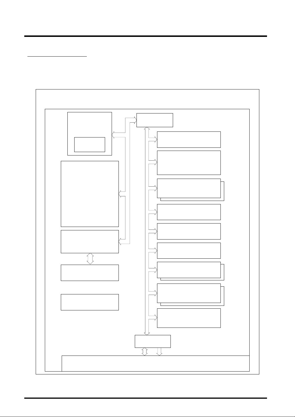
1.2 Block Diagram
1.2 Block Diagram
Figure 1.2.1 shows a block diagram of the 32172/32173. The features of each block are outlined in
Tables 1.2.1 to 1.2.3.
32172
32173
Internal Bus
M32R CPU Core
(max 40MHz)
Multiplieraccumulator
(32 x 16+56)
Internal Flash Memory
(256KB)
Interface
(A-D0: 10-bit A-D, 8 channels)
(A-D1: 10-bit A-D, 4 channels)
Internal 32-bit Bus
DMAC
(10 channels)
Input/output Timer
(26 channels)
A-D Converter x 2
Serial I/O
(8 channels)
Overview
Internal RAM
(M32172F2 : 16KB)
(M32173F2 : 32KB)
Real-time Debugger
(RTD)
PLL Clock Generating
Circuit
Figure 1.2.1 Block Diagram
Interrupt Controller
(interrupt sources in 8 levels)
Internal 16-bit Bus
External Bus
Interface
Input/output Ports (JTAG), 99 lines
Wait Controller
Full CAN
(2 channels)
D-A Converter x 2
(8 bits)
PD Controller
AddressData
1-7 Rev.1.0
Page 28

1
Table 1.2.1 Features of the M32R Family CPU Core
Functional Block Features
M32R family • Bus specifications
CPU core Basic bus cycle: 25 ns (when CPU clock = 40 MHz)
Logical address space: 4 Gbytes linear
External extended area: Maximum 4 Mbytes
External data bus: 16 bits
• Implementation: Five-stage pipelined processing
• CPU core internally configured in 32 bits
• Register configuration
General-purpose register: 32 bits x 16
Control register: 32 bits x 5
• Instruction set
16-bit/32-bit instruction formats
83 discrete instructions/6 addressing modes
• Built-in multiplier-accumulator (32 x 16 + 56)
Overview
1.2 Block Diagram
Table 1.2.2 Features of the Internal Memory
Functional Block Features
RAM • Capacity
M32172F2: 16 Kbytes
M32173F2: 32 Kbytes
• No-wait access
• By using the RTD (Real-time Debugger), the internal RAM can be accessed for
data read or rewrite from the outside, independently of the M32R.
Flash memory • Capacity: 256 Kbytes
• No-wait access
• Durability: Can be rewritten 100 times
1-8 Rev.1.0
Page 29

1
1.2 Block Diagram
Table 1.2.3 Features of Internal Peripheral I/Os
Functional Block Features
DMA • 10-channel DMA
• Supports data transfer between internal peripheral I/Os, between internal RAMs,
and between internal peripheral I/O and internal RAM
• Capable of fast DMA transfer when used in combination with internal peripheral I/O
• Capable of cascaded operation between DMA channels (starting DMA transfer on
a channel at the end of transfer on another)
Timer • 26-channel multifunction timers
• 16 channels of 16-bit output related timers, 6 channels of 16-bit input related
timers, and 4 channels of 32-bit input related timers
• Flexible timer configuration is possible by interconnecting each timer channel
A-D converter • One 8-channel A-D converter and one 4-channel A-D converter, both capable of
10-bit resolution
• Supports comparator mode
• Can generate an interrupt or start DMA transfer at completion of A-D conversion
• Can monitor pin levels on a total of 20 channels (with reduced accuracy, however)
Serial I/O • 8-channel serial I/O
• Can be set for clock-synchronized serial I/O or UART
• Capable of fast data transfer at 2 Mbits/second during clock-synchronized mode or
156 Kbits/second during UART mode
Real-time debugger • Can rewrite/monitor the internal RAM by command input from the outside,
independently of the CPU
• Comes with dedicated clock-synchronized serial port
Interrupt controller • Controls interrupt requests from internal peripheral I/Os
• Eight priority levels including interrupt-disabled state
Wait controller • Controls wait state when accessing external extended area
• Inserts 1 to 4 wait cycles by software setting + extends wait period by external
____
WAIT signal input
Clock PLL • Multiply-by-4 clock generating circuit
• CPU clock of maximum 40 MHz (CPU, internal ROM, and internal RAM access)
• Internal peripheral clock of maximum 20 MHz (peripheral module access)
• Maximum external input clock frequency of 10.0 MHz
D-A converter • Two channels of 8-bit resolution D-A converters
D-A0 converter: D-A output, successive data output function, 256-byte output
buffer available
D-A1 converter: D-A output only
PD Controller • Two blocks of PD sensor-accommodating timers and various arithmetic circuits for
position predictive operation
• 16-bit input measurement timer: 4 channels; 16-bit input related timer: 4 channels
• When not using the PD circuit, the above timers can be used as input
measurement timers or input event counters
CAN • Two blocks of CAN modules, each with 16-channel message slots
JTAG • Boundary scan function, Mitsubishi original SDI debug function included
Overview
1-9 Rev.1.0
Page 30
1
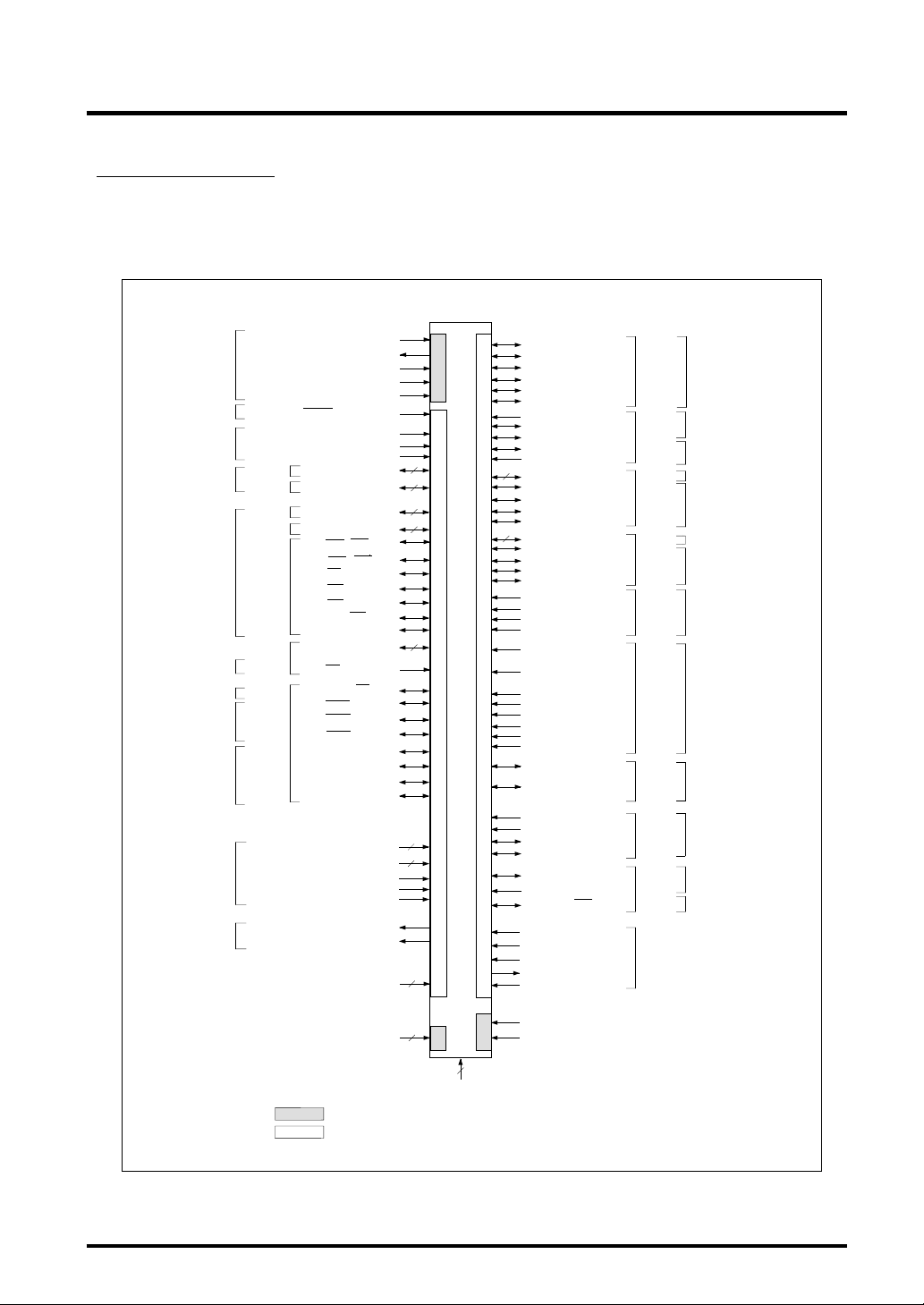
1.3 Pin Functions
1.3 Pin Functions
Figure 1.3.1 shows a pin function diagram of the 32172/32173. Table 1.3.1 provides a description
of pin functions.
Overview
Clock
Reset
Mode
Data bus
Address bus
Bus control
Interrupt
controller
Clock
Bus control
serial I/O
Realtime
debugger
A-D
converter
D-A
converter
Port 0
Port 1
Port 2
Port 3
Port 4
Port 6
Port 7
XIN
XOUT
VCNT
OSC-VCC
OSC-VSS
RESET
MOD0
MOD1
FP
P00 — P07/DB0 — DB7
P10 — P17/DB8 — DB15
P20 — P27 / A23 — A30
P30 — P37 / A15 — A22
P41 / BLW / BLE
P42 / BHW / BHE
P43 / RD
P44 / CS0
P45 / CS1
P46 / A13 / CS3
P47 / A14
P61 — P63
P64 / SBI
P70 / BCLK / WR
P71 / WAIT
P72 / HREQ
P73 / HACK /TXD3
P74 / RTDTXD
P75 / RTDRXD
P76 / RTDACK
P77 / RTDCLK
AD0IN0 — AD0IN7
AD1IN0 — AD1IN3
AVCC0
AVSS0
VREF0
DA0 (/ AD1IN4)
DA1 (/ AD1IN5)
VCCE
8
8
8
8
3
8
4
4
3.3V (Note)
5V
5V (Note)
M32172F2VFP, M32173F2VFP
P82 / TXD0
P83 / RXD0
P84 / SCLKI 0 / SCLKO 0
P85 / TXD1
P86 / RXD1
P87 / SCLKI 1 / SCLKO 1
P93 / RXD3 (/ AD0IN8)
P94 / TXD6
P95 / RXD6
P96 / CTX1
P97 / CRX1
4
P100 — P103 / TO8 — TO11
P104 / TO12 / SCLKI4
P105 / TO13 / SCLKO4
P106 / TO14 / TXD4
P107 / TO15 / RXD4
4
P110 — P113 / TO0 — TO3
P114 / TO4/ SCLKI5
P115 / TO5 / SCLKO5
P116 / TO6 / TXD5
P117 / TO7 / RXD5
P124 / TIN0A (/ AD0IN9)
P125 / TIN0B (/ AD1IN9)
P126 / TIN1A (/ AD0IN10)
P127 / TIN1B (/ AD1IN10)
P130 / TIN16 / PWMOFF0
(/AD0IN11)
P131 / TIN17 / PWMOFF1
(/AD1IN11)
P132 / TIN18 (/ AD0IN12)
P133 / TIN19 (/ AD1IN12)
P134 / TIN20 (/ AD0IN13)
P135 / TIN21 (/ AD1IN13)
P136 / TIN22 (/ AD0IN14)
P137 / TIN23 (/ AD1IN14)
P150 / TIN8 / TXD7
(/AD0IN15)
P153 / TIN9 / RXD7
(/AD1IN15)
P172 / TIN10 (/ AD1IN6)
P173 / TIN11 (/ AD1IN7)
P174 / TXD2
P175 / RXD2
P220 / CTX0
P221 / CRX0
P225 / A12 / CS2
JTMS
JTCK
JTRST
JTDO
JTDI
Port 8
Port 9
Port 10
Port 11
Port 12
Port 13
Port 15
Port 17
Port 22
JTAG
Serial I/O
Serial I/O
CAN
Input/output
timer
Input/output
timer serial I/O
Input/output
timer
Input/output
timer serial I/O
PD module
(A-D converter)
Input/output
timer
(A-D converter)
Input/output
timer serial I/O
(A-D converter)
Input/output
timer serial I/O
(A-D converter)
CAN
Bus control
address bus
3.3V
VDD
FVCC
Note
VCCI
: The [3.3V] blocks operate with a 3.3 V power supply.
3.3V
: The [5V] blocks operate with a 5 V or 3.3 V power supply.
5V
3
3.3V
5
VSS
Figure 1.3.1 Pin Function Diagram of 144LQFP Package
1-10 Rev.1.0
Page 31

1
Overview
1.3 Pin Functions
Clock
Reset
Mode
Data bus
Address bus
Bus control
Interrupt
controller
Clock
Bus control
serial I/O
Realtime
debugger
A-D
converter
D-A
converter
DEBUG
Port 0
Port 1
Port 2
Port 3
Port 4
Port 6
Port 7
Note
XIN
XOUT
VCNT
OSC-VCC
OSC-VSS
RESET
MOD0
MOD1
FP
P00 — P07/DB0 — DB7
P10 — P17/DB8 — DB15
P20 — P27 / A23 — A30
P30 — P37 / A15 — A22
P41 / BLW / BLE
P42 / BHW / BHE
P43 / RD
P44 / CS0
P45 / CS1
P46 / A13 / CS3
P47 / A14
P61 — P63
P64 / SBI
P70 / BCLK / WR
P71 / WAIT
P72 / HREQ
P73 / HACK /TXD3
P74 / RTDTXD
P75 / RTDRXD
P76 / RTDACK
P77 / RTDCLK
AD0IN0 — AD0IN7
AD1IN0 — AD1IN3
AVCC0
AVSS0
VREF0
DA0 (/ AD1IN4)
DA1 (/ AD1IN5)
TRCLK
TRSYNC
TRDATA
DBI
EVENT0
EVENT1
VCCE
VCCI
: The [3.3V] blocks operate with a 3.3 V power supply.
3.3V
: The [5V] blocks operate with a 5 V power supply.
5V
8
8
8
8
3
8
4
8
4
3
3.3V (Note)
5V (Note)
M32172F2VWG, M32173F2VWG
3.3V
5
VSS
P82 / TXD0
P83 / RXD0
P84 / SCLKI 0 / SCLKO 0
P85 / TXD1
P86 / RXD1
P87 / SCLKI 1 / SCLKO 1
P93 / RXD3 (/ AD0IN8)
P94 / TXD6
P95 / RXD6
P96 / CTX1
P97 / CRX1
4
P100 — P103 / TO8 — TO11
P104 / TO12 / SCLKI4
P105 / TO13 / SCLKO4
P106 / TO14 / TXD4
P107 / TO15 / RXD4
4
P110 — P113 / TO0 — TO3
P114 / TO4/ SCLKI5
P115 / TO5 / SCLKO5
P116 / TO6 / TXD5
P117 / TO7 / RXD5
P124 / TIN0A (/ AD0IN9)
5V
P125 / TIN0B (/ AD1IN9)
P126 / TIN1A (/ AD0IN10)
P127 / TIN1B (/ AD1IN10)
P130 / TIN16 / PWMOFF0
(/AD0IN11)
P131 / TIN17 / PWMOFF1
(/AD1IN11)
P132 / TIN18 (/ AD0IN12)
P133 / TIN19 (/ AD1IN12)
P134 / TIN20 (/ AD0IN13)
P135 / TIN21 (/ AD1IN13)
P136 / TIN22 (/ AD0IN14)
P137 / TIN23 (/ AD1IN14)
P150 / TIN8 / TXD7
(/ AD0IN15)
P153 / TIN9 / RXD7
(/ AD1IN15)
P172 / TIN10 (/ AD1IN6)
P173 / TIN11 (/ AD1IN7)
P174 / TXD2
P175 / RXD2
P220 / CTX0
P221 / CRX0
P225 / A12 / CS2
JTMS
JTCK
JTRST
JTDO
JTDI
VDD
FVCC
3.3V
Port 8
Port 9
Port 10
Port 11
Port 12
Port 13
Port 15
Port 17
Port 22
JTAG
Serial I/O
Serial I/O
CAN
Input/output timer
Input/output timer
serial I/O
Input/output timer
Input/output timer
serial I/O
PD module
(A-D converter)
Input/output timer
(A-D converter)
Input/output timer
serial I/O
(A-D converter)
Input/output timer
serial I/O
(A-D converter)
CAN
Bus control
address bus
Figure 1.3.2 Pin Function Diagram of 175FBGA Package
1-11 Rev.1.0
Page 32

1
1.3 Pin Functions
Table 1.3.1 Description of Pin Functions (1/6)
Classification Pin Name Description Type Function
Power supply VCCE Power supply –– Supplies power to external I/O ports (5 V).
VCCI Power supply –– Supplies power to the internal logic (3.3 V).
VDD RAM power supply –– Power supply pin for internal RAM backup (3.3 V).
FVCC Flash power supply –– Power supply pin for the internal flash memory (3.3 V).
VSS Ground –– Connect all VSS to ground (GND).
Clock XIN, Clock Input Clock input/output pin. With a PLL-based
XOUT Output frequency multiplier circuit included, enter a clock with
1/4 the operating frequency (XIN input = 10.0 MHz for
the CPU clock of 40 MHz).
______
BCLK/WR System Output When this signal is System Clock (BCLK), it outputs a
clock clock whose is twice that of extemal inpout clock.
OSC-VCC Power supply –– Power supply for the PLL circuit. Connect OSC-VCC to
OSC-VSS Ground –– Connect OSC-VSS to ground.
VCNT PLL control Input PLL circuit control pin. Connect a resistor and capacitor
Reset
Mode MOD0 Mode Input Sets operation mode.
Address A12-A30 Address Output To allow four blocks of up to 1 MB memory space to
bus bus be connected external to the chip, 19 address lines
_____
RESET Reset Input Resets the internal circuits.
MOD1 FP MOD0 MOD1 Mode
Use this clock for external synchronized design.
(BCLK output = 20 MHz when CPU clock operates at
40 MHz).
When this signal is Write (WR), during extemal write
access it indicates the valid data on the data bus to
transfer.
input clock (BCLK output = 20 MHz when the external
input clock is 10 MHz).
the power supply (3.3 V).
to this pin. (For details about an external circuit, refer to
Section 20.1.1, "Example of an Oscillator Circuit."
X 0 0 Single-chip mode
X 0 1 External extended mode
0 1 0 Processor mode
1 1 0 Boot mode
X 1 1 (Reserved)
(A12-A30) are provided. A31 is not output to the
outside.
__
Overview
Note: For details about boot mode, refer to Chapter 6, "Internal Memory."
1-12 Rev.1.0
Page 33

1
1.3 Pin Functions
Table 1.3.1 Description of Pin Functions (2/6)
Classification Pin Name Description Type Function
Data bus DB0-DB15 Data bus Input/Output 16-bit data bus for connecting external devices. In write
cycle, the CPU outputs BHW/BHE and BLW/BLE
indicating the valid byte position to write on the 16-bit
data bus. In read cycle, the CPU always reads data
from the full 16-bit data bus. However, data at only the
valid byte position is transferred to the internal circuit
Bus control
Input/ TIN8-TIN11, Timer input Input Input/output timer input pin.
output timer TIN16-TIN23
Interrupt
controller interrupt controller.
___ ___
CS0, CS1 Chip select Output Chip select signal for external devices. For details about
___ ___
CS2, CS3 areas for which the chip select signal is output, refer to
__
RD Read Output This signal is output when reading an external device.
___
___
BHW/BHE Byte high Output Indicates the byte position to which valid data will be
___
___
BLW/BLE Byte low Output
____
WAIT Wait Input
____
HREQ Hold request Input This input pin is provided for external devices to request
____
HACK Hold Output
TO0-TO15 Timer output Output Input/output timer output pin.
___
SBI System breakInput System Break Interrupt (SBI) input pin for the interrupt
write/enable
write/enable
acknowledge a hold state and relinquished control of the external bus.
of the M32R.
Chapter 3, "Address Space."
transferred when writing to an external device.BHW/
___
BHE is output for the upper address side (D0-D7 is
valid), while BLW/BLE is output for the lower address
side (D8-D15 is valid).
If input on WAIT is low when the M32R accesses an
external device, the wait cycle is extended.
control of the external bus. If input on the HREQ pin is
pulled low, the M32R goes to a hold state.
This signal is used to indicate that the M32R has entered
___
____
___
___
___
Overview
___
___
___
____
1-13 Rev.1.0
Page 34

1
1.3 Pin Functions
Table 1.3.1 Description of Pin Functions (3/6)
Classification Pin Name Description Type Function
PD controller TIN0A, TIN0B Timer input Input PD0 sensor interface and timer input pin.
TIN1A, TIN1B Timer input Input PD1 sensor interface and timer input pin.
A-D converterAVCC0 Analog power –– AVCC0 is the power supply for the A-D and D-A
supply converters. Connect AVCC0 to the power supply (5 V).
AVSS0 Analog ground –– AVSS0 is the analog ground for the A-D and D-A
converters. Connect AVSS0 to ground.
VREF0 Reference voltage Input VREF0 is the reference voltage input pin for the A-D
input and D-A converters (5 V).
AD0IN0 Analog input Input 8-channel analog input pins for the A-D0 converter.
– AD0IN7
AD1IN0 Analog input Input 4-channel analog input pins for the A-D1 converter.
– AD1IN3
(/AD0IN8) Analog input Input
– (AD0IN15,)
(/AD1IN4)
– (/AD1IN15)
D-A DA0 Analog output Output Analog output pin for the D-A0 converter.
converter DA1 Analog output Output Analog output pin for the D-A1 converter.
Serial I/O SCLKI0/ UART transmit/ Input/ For UART mode: These pins output a clock derived
SCLKO0, receive clock Output from BRG by dividing it by 2.
SCLKI1/ output or CSIO For CSIO mode: These pins accept as input the
SCLKO1 transmit/receive
clock input/output or output the transmit/receive clock when an internal
20-channel analog input pins used to monitor the pin levels.
transmit/receive clock when an external clock is selected
clock is selected
Overview
1-14 Rev.1.0
Page 35

1
Table 1.3.1 Description of Pin Functions (4/6)
Overview
1.3 Pin Functions
Classification
Serial I/O SCLKI4, Clock output Input For UART mode: Use inhibited (in input state)
Pin Name Description Type Function
SCLKI5 For CSIO mode: Transmit/receive clock input when
external clock is selected
SCLKO4, Clock output Output For UART mode: Clock output derived from BRG by
SCLKO5 dividing it by 2
For CSIO mode: Transmit/receive clock output
TXD0-TXD7 Transmit data Output Serial I/O transmit data output pins.
RXD0-RXD7 Received data Input Serial I/O received data input pins.
1-15 Rev.1.0
Page 36

1
1.3 Pin Functions
Table 1.3.1 Description of Pin Functions (5/6)
Classification Pin Name Description Type Function
Real-time RTDTXD Transmit data Output Serial data output pin for the real-time debugger.
debugger RTDRXD Received data Input Serial data input pin for the real-time debugger.
RTDCLK Clock input Input Serial data transmit/receive clock input pin for
the real-time debugger.
RTDACK Acknowledge Output Outputs a low-level pulse synchronously with the
first clock cycle of the real-time debugger's serial
data output word. The low-level pulse width
indicates the type of command/data received by
the real-time debugger.
Flash only FP Flash Protect Input This is a mode pin which has the function to
protect the flash memory against E/W in hardware.
CAN
JTAG JTMS Test mode Input Test mode select input to control the state
Input/output P00-P07 Input/output port 0 Input/Output Programmable input/output port.
port P10-P17 Input/output port 1 Input/Output Programmable input/output port.
(Note) P20-P27 Input/output port 2 Input/Output Programmable input/output port.
CTX0,CTX1
CRX0,CRX1
JTCK Clock Input Clock input for the debug module and test circuit.
JTRST Test reset Input Test reset input to initialize the test circuit
JTDI Serial input Input This pin takes in the test instruction code or
JTDO Serial output Output This pin outputs the test instruction code or
P30-P37 Input/output port 3 Input/Output Programmable input/output port.
Data output Output These pins output the data from the CAN module.
Data input Input These pins take in the data for the CAN module.
transition of the test circuit.
asynchronously.
test data serially.
test data serially.
Overview
1-16 Rev.1.0
Page 37

1
Table 1.3.1 Description of Pin Functions (6/6)
Classification Pin Name Description Type Function
Input/output P41-P47 Input/output port 4 Input/Output Programmable input/output port.
port
(Note 1) (However, P64 is an input-only port.)
P61-P64 Input/output port 6 Input/Output Programmable input/output port.
P70-P77 Input/output port 7 Input/Output Programmable input/output port.
P82-P87 Input/output port 8 Input/Output Programmable input/output port.
P93-P97 Input/output port 9 Input/Output Programmable input/output port.
(However, P93 and P97 are input-only ports.)
P100-P107 Input/output port 10 Input/Output Programmable input/output port.
P110-P117 Input/output port 11 Input/Output Programmable input/output port.
P124-P127 Input/output port 12 Input/Output Input-only port.
P130-P137 Input/output port 13 Input/Output Input-only port.
P150, P153 Input/output port 15 Input/Output Programmable input/output port.
P172-P175 Input/output port 17 Input/Output Programmable input/output port.
(However, P172 and P173 are input-only pins.)
P220,P221 Input/output port 22 Input/Output Programmable input/output port.
P225 (Note 2) (However, P22 is a CAN input-only pin.)
Overview
1.3 Pin Functions
Note 1: Input/output port 5 is reserved for future use. Input/output ports 14, 16, 18, 19, 20, and 21 are
nonexistent.
Note 2: Use of P225 requires caution because it has a debug event function.
1-17 Rev.1.0
Page 38

1
1.4 Pin Layout
1.4 Pin Layout
Figure 1.4.1 shows a pin layout diagram of the 32172/32173. Table 1.4.1 lists a pin arrangement of
the 32172/32173.
Overview
JTMS
JTCK
JTRST
JTDO
P103/TO11
P104/TO12/SCLKI4
P105/TO13/SCLKO4
P106/TO14/TXD4
P107/TO15/RXD4
P124/TIN0A (/AD0IN9)
P125/TIN0B (/AD1IN9)
P126/TIN1A (/AD0IN10)
P127/TIN1B (/AD1IN10)
P130/TIN16/PWMOFF0 (/AD0IN11)
P131/TIN17/PWMOFF1 (/AD1IN11)
P132/TIN18 (/AD0IN12)
P133/TIN19 (/AD1IN12)
P134/TIN20 (/AD0IN13)
P135/TIN21 (/AD1IN13)
P136/TIN22 (/AD0IN14)
P137/TIN23 (/AD1IN14)
P150/TIN8/TXD7 (/AD0IN15)
P153/TIN9/RXD7 (/AD1IN15)
VCCI
VCCE
P41/ BLW / BLE
P42/ BHW / BHE
VCCI
VSS
P43/ RD
P44/ CS0
P45/ CS1
P46/A13/ CS3
P47/A14
P220/CTX0
JTDI
P117/TO7/RXD5
P116/TO6/TXD5
104
103
5
6
XOUT
OSC-VCC
P112/TO2
VSS
P114/TO4/SCLKI5
P111/TO1
P110/TO0
P115/TO5/SCLKO5
P113/TO3
99
98
97
102
96
101
100
M32172F2VFP
M32173F2VFP
8
9
7
10
11
12
13
VCNT
P30/A15
P31/A16
P32/A17
P33/A18
P34/A19
P35/A20
VCCE
95
94
14
15
P36/A21
P37/A22
FP
MOD0
MOD1
93
92
17
16
P20/A23
P21/A24
RESET
91
18
P22/A25
P97/CRX1
P96/CTX1
90
89
19
20
VCCE
P23/A26
P94/TXD6
P93/RXD3 (/AD0IN8)
P95/RXD6 (/AD1IN8)
P77/RTDCLK
P76/RTDACK
P75/RTDRXD
86
85
84
83
88
87
21
22
23
24
25
26
VSS
P24/A27
P25/A28
P26/A29
P27/A30
P00/DB0
P74/RTDTXD
P72/ HREQ
P71/ WAIT
P73/ HACK /TXD3
82
81
80
79
27
28
29
30
P01/DB1
P02/DB2
P03/DB3
P04/DB4
P70/BCLK / WR
P64/ SBI
P63
P62
78
77
76
75
31
32
33
34
P10/DB8
P05/DB5
P06/DB6
P07/DB7
P61
74
35
P11/DB9
FVCC
73
36
P12/DB10
72
71
70
69
68
67
66
65
64
63
62
61
60
59
58
57
56
55
54
53
52
51
50
49
48
47
46
45
44
43
42
41
40
39
38
37
VSS
P87/SCLKI1/SCLKO1
P86/RXD1
P85/TXD1
P84/SCLKI0/SCLKO0
P83/RXD0
P82/TXD0
VCCE
P175/RXD2
P174/TXD2
VSS
VCCI
AVSS0
P173/TIN11 (/AD1IN7)
P172/TIN10 (/AD1IN6)
DA1 (/AD1IN5)
DA0 (/AD1IN4)
AD1IN3
AD1IN2
AD1IN1
AD1IN0
AD0IN7
AD0IN6
AD0IN5
AD0IN4
AD0IN3
AD0IN2
AD0IN1
AD0IN0
AVCC0
VREF0
P17/DB15
P16/DB14
P15/DB13
P14/DB12
P13/DB11
P101/TO9
P100/TO8
P102/TO10
VDD
108
107
106
105
109
110
111
112
113
114
115
116
117
118
119
120
121
122
123
124
125
126
127
128
129
130
131
132
133
134
135
136
137
138
139
140
141
142
143
144
1
2
3
4
XIN
OSC-VSS
P221/CRX0
P225/A12/CS2
(Note)
Package: 144P6Q (0.5 mm pitch)
Note: Use caution when using a pin because it has a debug event function.
Figure 1.4.1 Pin Layout Diagram of the M32172F2VFP/M32173F2VFP (Top View)
1-18 Rev.1.0
Page 39

1
Table 1.4.1 Pin Arrangement of the 144LQFP Package (1/2)
No. Pin Name No. Pin Name No. Pin Name
1 P221/CRX0 31 P05/DB5 61 VCCI
2
P225/A12/CS2 32 P06/DB6 62 VSS
3 OSC-VSS 33 P07/DB7 63 P174/TXD2
4 XIN 34 P10/DB8 64 P175/RXD2
5 XOUT 35 P11/DB9 65 VCCE
6 OSC-VCC 36 P12/DB10 66 P82/TXD0
7 VCNT 37 P13/DB11 67 P83/RXD0
8 P30/A15 38 P14/OB12 68 P84/SCLKI0/SCLKO0
9 P31/A16 39 P15/DB13 69 P85/TXD1
10 P32/A17 40 P16/DB14 70 P86/RXD1
11 P33/A18 41 P17/DB15 71 P87/SCLKI1/SCLKO1
12 P34/A19 42 VREF0 72 VSS
13 P35/A20 43 AVCC0 73 FVCC
14 P36/A21 44 AD0IN0 74 P61
15 P37/A22 45 AD0IN1 75 P62
16 P20/A23 46 AD0IN2 76 P63
17 P21/A24 47 AD0IN3 77
18 P22/A25 48 AD0IN4 78__P70/BCLK/WR
19 P23/A26 49 AD0IN5 79
20 VCCE 50 AD0IN6 80
21 VSS 51 AD0IN7 81
22 P24/A27 52 AD1IN0 82 P74/RTDTXD
23 P25/A28 53 AD1IN1 83 P75/RTDRXD
24 P26/A29 54 AD1IN2 84 P76/RTDACK
25 P27/A30 55 AD1IN3 85 P77/RTDCLK
26 P00/DB0 56 DA0 (/AD1IN4) 86 P93/RXD3 (/AD0IN8)
27 P01/DB1 57 DA1 (/AD1IN5) 87 P94/TXD6
28 P02/DB2 58 P172/TIN10 (/AD1IN6) 88 P95/RXD6 (/AD1IN8)
29 P03/DB3 59 P173/TIN11 (/AD1IN7) 89 P96/CTX1
30 P04/DB4 60 AVSS0 90 P97/CRX1
___
___
P64/SBI
____
P71/WAIT
____
P72/HREQ
____
P73/HACK/TXD3
Overview
1.4 Pin Layout
1-19 Rev.1.0
Page 40

1
Table 1.4.2 Pin Arrangement of the 144LQFP Package (2/2)
No. Pin Name No. Pin Name No. Pin Name
_____
91
RESET 111 JTRST 131 P137/TIN23 (/AD1IN14)
92 MOD0 112 JTDO 132 VCCE
93 MOD1 113 JTDI 133 P150/TIN8/TXD7 (/AD0IN15)
94 FP 114 P103/TO11 134 P153/TIN9/RXD7 (/AD1IN15)
95 VCCE 115 P104/TO12/SCLKI4 135
96 VSS 116 P105/TO13/SCLKO4 136
97 P110/TO0 117 P106/TO14/TXD4 137 VCCI
98 P111/TO1 118 P107/TO15/RXD4 138 VSS
99 P112/TO2 119 P124/TIN0A (/ADIN9) 139__P43/RD
100 P113/TO3 120 P125/TIN0B (/AD1IN9) 140
101 P114/TO4/SCLKI5 121 P126/TIN1A (/AD0IN10) 141
102 P115/TO5/SCLKO5 122 P127/TIN1B (/AD1IN10) 142
103 P116/TO6/TXD5 123 VCCI 143 P47/A14
104 P117/TO7/RXD5 124
105 P100/TO8 125
106 P101/TO9 126 P132/TIN18 (/AD0IN12)
107 P102/TO10 127 P133/TIN19 (/AD1IN12)
108 VDD 128 P134/TIN20 (/AD0IN13)
109 JTMS 129 P135/TIN21 (/AD1IN13)
110 JTCK 130 P136/TIN22 (/AD0IN14)
P130/TIN16/PWMOFF0 (/AD0IN11)
P131/TIN17/PWMOFF1 (/AD0IN11)
144 P220/CTX0
___ ___
P41/BLW/BLE
___ ___
P42/BHW/BHE
___
P44/CS0
___
P45/CS1
P46/A13/CS3
___
Overview
1.4 Pin Layout
1-20 Rev.1.0
Page 41

1
P117
JTRST JTCK
15
JTDO JTMS VDD P100/TO8 P111/TO1 FP RESET
14
N.C. N.C. N.C. P101/TO9
13
12
11
10
9
8
7
6
5
P103/TO11
P106/TO14
/TXD4
DBI
EVENT1
P131/TIN17
/PWMOFF1
(/AD1IN11)
P135
/TIN21
(/AD1IN13)
P150/TIN8
/TXD7
(/AD0IN15)
VCCI
/SCLKO4
(/AD1IN9)
(/AD1IN10)
(/AD0IN12)
(/AD0IN14)
P153/TIN9
(/AD1IN15)
N.C.
JTDI
P105 P104 P107
/TO12
/TO13
/SCLKI4
P125 P124 P126
/TIN0B
/TIN0A
(/AD0IN9)
P127
EVENT0
/TIN1B
P132 P133
/TIN18
P136
/TIN22
/RXD7
VSS
/TIN19
(/AD1IN12)
P137
/TIN23
(/AD1IN14)
P41/BLW
/BLE
P43/RD
P130/TIN16
/PWMOFF0
/TO7
/RXD5
N.C.
/TO15
/RXD4
/TIN1A
(/AD0IN10)
VCCI
(/AD0IN11)
P134
/TIN20
(/AD0IN13)
VCCE
P42/BHW
/BHE
P114
/TO4
P110/TO0P102/TO0
/SCLKI5
P115/TO5
/SCLKO5
P116/TO6
P112/TO2 VCCE MOD0 P94/TXD6
/TXD5
P113/TO3
VSS
TRDATA7
M32172F2VWG
M32173F2VWG
MOD1
TRDATA6
P97/CRX1
TRDATA5
P95
/RXD6
(/AD1IN8)
P96/CTX1
P93
/RXD3
(/AD0IN8)
P77
/RTDCLK
P76
/RTDACK
TRDATA4
P74
P71/WAIT P63 FVCC N.C.
/RTDTXD
P70/BCLK
P73/HACK
/TXD3
/WR
P72/HREQ
P64/SB1
/SCLKI1
/SCLKO1
P75/RTDRXD
N.C.
P174/TXD2
TRDATA0
P173
/TIN11
(/AD1IN7)
P172
/TIN10
(/AD1IN6)
AD1IN2
AD0IN6
AD0IN2
P85/TXD1
P82/TXD0
TRDATA3
VSS
AD1IN3
AD0IN7
AD0IN3
AVCC0
Overview
1.4 Pin Layout
P62 P61
P87
/SCLKI0
/SCLKO0
TRDATA2
(/AD1IN14)
AD0IN4
AD0IN0
VSS
N.C. P86/RXD1
P84
P83/RXD0
P175/RXD2
VCCE
TRDATA1
VCCI
AVSS0
DA1
DA0
(/AD1IN15)
AD1IN0
AD1IN1
AD0IN5
AD0IN1
4
N.C.
N.C.
3
P45/CS1
2
P47/A14
1
ADE
N.C.
N.C.
P46/A13
/CS3
N.C.
P44/CS0
P220/CTX0
P221/CRX0
C
N.C.
P225/A12
/CS2
OSC-VSS
XIN
P30/A15
XOUT
OSC-VCC
VCNT
P34/A19
P37/A22
P31/A16
P35/A20
P32/A17
TRCLK
P33/A18
P36/A21
FGH
Figure 1.4.2 Pin Layout Diagram (Top View)
P23/A26
P20/A23
P21/A24
P22/A25
VCCE
P24/A27
TRSYNC
VSS
J
P25/A28
P00/DB0
P27/A30
P26/A29
KLMNPRB
P01/DB1
P04/DB4
P03/DB3
P02/DB2
N.C.
P07/DB7
P06/DB6
P05/DB5
N.C.
P16/DB14
P11/DB9
P10/DB8
P17/DB15
N.C. N.C.
P12/DB10
P13/DB11
VREF0
P15/DB13
P14/DB12
1-21 Rev.1.0
Page 42

1
Table 1.4.3 Pin Arrangement of the 175FBGA Package (1/2)
No. Pin Name No. Pin Name No. Pin Name
A1 –– D1 XIN G1 P36/A21
A2
A3 N.C. D3
A4 N.C. D4 N.C. G4 P37/A22
A5 VCCI D5
A6 P150/TIN8/TXD7(/AD0IN15) D6 VCCE G6 ––
A7 P135/TIN21(/AD1IN13) D7 P134/TIN20(/AD0IN13) G7 ––
A8
A9 EVENT1 D9 VCCI G9 ––
A10 DBI D10 P126/TIN1A(/AD0IN10) G10 ––
A11 P106/TO14/TXD4 D11 P107/TO15/RXD4 G11 ––
A12 P103/TO11 D12 N.C. G12 TRDATA7
A13 N.C. D13 P101/TO9 G13 VCCE
A14 JTDO D14 P100/TO8 G14 FP
A15 JTRST D15 P117/TO7/RXD5 G15 MOD1
B1
B2 P47/A14 E2 OSC-VCC H2 P21/A24
B3 N.C. E3 XOUT H3 P20/A23
B4 N.C. E4 P30/A15 H4 P23/A26
B5 VSS E5 –– H5 ––
B6 P153/TIN9/RXD7(/AD1IN15) E6 –– H6 ––
B7 P136/TIN22(/AD0IN14) E7 –– H7 ––
B8 P132/TIN18(/AD01N12) E8 –– H8 ––
B9 P127/TIN1B(/AD1IN10) E9 –– H9 ––
B10 P125/TIN0B(/AD1IN9) E10 –– H10 ––
B11 P105/TO13/SCLKO4 E11 –– H11 ––
B12 JTDI E12 P113/TO3 H12 P97/CRX1
B13 N.C. E13 P116/TO6/TXD5 H13 MOD0
B14 JTMS E14 P115/TO5/SCLKO5 H14
B15 JTCK E15 P114/TO4/SCLKI5 H15 TRDATA6
C1 P221/CRX0 F1 P33/A18 J1 VSS
C2 P210/CTX0 F2 P32/A17 J2 TRSYNC
C3
C4 N.C. F4 P34/A19 J4 VCCE
C5__P43/RD F5 –– J5 ––
C6
C7 P137/TIN23(/AD1IN14) F7 –– J7 ––
C8 P133/TIN19(/AD1IN12) F8 –– J8 ––
C9 EVENT0 F9 –– J9 ––
C10 P124/TIN0A(/AD0IN9) F10 –– J10 ––
C11 P104/TO12/SCLK14 F11 –– J11 ––
C12 N.C. F12 VSS J12 P96/CTX1
C13 N.C. F13 P112/TO2 J13 P94/TXD6
C14 VDD F14 P111/TO1 J14 P95/RXD6(/AD1IN8)
C15 P102/TO10 F15 P110/TO0 J15 TRDATA5
______
P45/CS1 D2 OSC-VSS G2 TRCLK
P225/A12/CS2 G3 P35/A20
P42/BHW/BHE G5 ––
P131/TIN17/PMWOFF1(/AD1IN11)D8P130/TIN16/PWMOFF0(/AD0IN11)
______
___
______
___
P46/A13/CS3 E1 VCNT H1 P22/A25
P44/CS0 F3 P31/A16 J3 P24/A27
P41/BLW/BLE F6 –– J6 ––
___
______
___
G8 ––
____________
RESET
Overview
1.4 Pin Layout
1-22 Rev.1.0
Page 43

1
Table 1.4.4 Pin Arrangement of the 175FBGA Package (2/2)
No. Pin Name No. Pin Name No. Pin Name
K1 P26/A29 M1 P05/DB5 P1 P13/DB11
K2 P27/A30 M2 P06/DB6 P2 P12/DB10
K3 P00/DB0 M3 P07/DB7 P3 N.C.
K4 P25/A28 M4 N.C. P4 P17/DB15
K5 –– M5 AD0IN2 P5 AD0IN0
K6 –– M6 AD0IN6 P6 AD0IN4
K7 –– M7 AD1IN2 P7 AD1IN0
K8 –– M8 P172/TIN10(/AD1IN6) P8 DA0(/AD1IN14)
K9 –– M9 P173/TIN11(/AD1IN7) P9 VCCI
K10 –– M10 TRDATA0 P10 TRDATA2
K11 –– M11 P174/TXD2 P11 VCCE
K12 TRDATA4 M12 N.C. P12 P84/SCLKI0/SCLKO0
K13 P76/RTDACK M13
K14 P77/RTDCLK M14__P70/BCLK/WR P14 P61
K15 P93/RXD3(/AD0IN8) M15
L1 P02/DB2 N1 P10/DB8 R1 P14/DB12
L2 P03/DB3 N2 P11/DB9 R2 P15/DB13
L3 P04/DB4 N3 P16/DB14 R3 N.C.
L4 P01/DB1 N4 N.C. R4 VREF0
L5 –– N5 AVCC0 R5 AD0IN1
L6 –– N6 AD0IN3 R6 AD0IN5
L7 –– N7 AD0IN7 R7 AD1IN1
L8 –– N8 AD1IN3 R8 DA1(/AD1IN15)
L9 –– N9 VSS R9 AVSS0
L10 –– N10 TRDATA3 R10 TRDATA1
L11 –– N11 P82/TXD0 R11 P175/RXD2
L12 P75/RTDRXD N12 P85/TXD1 R12 P83/RXD0
L13
L14
L15 P74/RTDTXD N15 P63 R15 N.C.
____
P72/HREQ N13 P87/SCLKI1/SCLKO1 R13 P86/RXD1
____
P73/HACK/TXD3 N14 P62 R14 VSS
___
P64/SB1 P13 N.C.
____
P71/WAIT P15 FVCC
Overview
1.4 Pin Layout
1-23 Rev.1.0
Page 44

1
Overview
1.4 Pin Layout
*** This is a blank page ***
1-24 Rev.1.0
Page 45

CHAPTER 2CHAPTER 2
CPU
2.1 CPU Registers
2.2 General-purpose Registers
2.3 Control Registers
2.4 Accumulator
2.5 Program Counter
2.6 Data Formats
Page 46

2
2.1 CPU Registers
2.1 CPU Registers
The M32R has sixteen general-purpose registers, five control registers, an accumulator, and a
program counter. The accumulator is a 56-bit configuration, and all other registers are a 32-bit
configuration.
2.2 General-purpose Registers
General-purpose registers are 32 bits in width and there are sixteen of them (R0 to R15), which are
used to hold data and base addresses. Especially, R14 is used as a link register, and R15 is used
as a stack pointer. The link register is used to store the return address when executing a subroutine
call instruction. The stack pointer is switched between an interrupt stack pointer (SPI) and a user
stack pointer (SPU) depending on the value of the Processor Status Word register (PSW)'s stack
mode (SM) bit.
CPU
00
Note: The stack pointer is switched between an interrupt stack pointer (SPI) and a user stack pointer
(SPU) depending on the value of the PSW's SM bit.
Figure 2.2.1 General-purpose Registers
31 31
R0
R1
R2
R3
R4
R5
R6
R7
R8
R9
R10
R11
R12
R13
R14 (Link register)
R15 (Stack pointer) (Note)
2-2 Rev.1.0
Page 47

2
2.3 Control Registers
2.3 Control Registers
There are five control registers-Processor Status Word Register (PSW), Condition Bit Register
(CBR), Interrupt Stack Pointer (SPI), User Stack Pointer (SPU), and Backup PC (BPC).
Dedicated "MVTC" and "MVFC" instructions are used to set and read these control registers.
CPU
CRn
Notes 1: CRn (n = 0-3, 6) denotes control register numbers.
2: Dedicated "MVTC" and "MVFC" instructions are used to set and read the control registers.
Figure 2.3.1 Control Registers
0 31
CR0
CR1
CR2
CR3
CR6 Backup PC
Control Registers
PSW
CBR
SPI
SPU
BPC
Processor status Word Register
Condition Bit Register
Interrupt Stack Pointer
User Stack Pointer
2-3 Rev.1.0
Page 48

2
2.3 Control Registers
2.3.1 Processor Status Word Register: PSW (CR0)
The Processor Status Word Register (PSW) is used to indicate the status of the M32R. It consists
of a regularly used PSW field and a special BPSW field which is used to save the PSW field when
an EIT occurs.
The PSW field consists of several bits labeled Stack Mode (SM), Interrupt Enable (IE), and
Condition bit (C). The BPSW field consists of backup bits of the foregoing, i.e., Backup SM bit
(BSM), Backup IE bit (BIE), and Backup C bit (BC).
BPSW field PSW field
CPU
0(MSB)
PS
W
D Bit Name Function Initial R W
16 BSM (Backup SM) Holds the value of SM bit when EIT Indeterminate
is accepted.
17 BIE (Backup IE) Holds the value of IE bit when EIT Indeterminate
is accepted.
23 BC (Backup C) Holds the value of C bit when EIT Indeterminate
is accepted.
24 SM (Stack Mode) 0: Interrupt stack pointer is used. 0
1: User stack pointer is used.
25 IE (Interrupt Enable) 0: No interrupt is accepted. 0
1: Interrupt is accepted.
16 17 23 24 25
1587
SM IE CBCBSM BIE
(Note 1)
31(LSB)
00000000000000000000000000
31 C (Condition bit) Depending on instruction execution, it indicates 0
whether operation resulted in a carry, borrow, or overflow.
Note 1: "Initial" shows the state immediately after reset, R = O means the register is readable,
W = O means the register is writable.
Note 2: For changes of the state of each bit when an EIT event occurs, refer to Chapter 4, "EIT.”
2-4 Rev.1.0
Page 49

2
2.3 Control Registers
2.3.2 Condition Bit Register: CBR (CR1)
The Condition Bit Register (CBR) is created as a separate register from the PSW by extracting the
Condition bit (C) from it. The value written to the PSW C bit is reflected in this register. This register
is a read-only register (writes to this register by "MVTC" instruction are ignored).
0(MSB) 31(LSB)
0000000000000000000000000000000
CBR
2.3.3 Interrupt Stack Pointer: SPI (CR2) User Stack Pointer: SPU (CR3)
The Interrupt Stack Pointer (SPI) and User Stack Pointer (SPU) hold the current address of the
stack pointer. These registers can be accessed as general-purpose register R15. In this case,
whether R15 is used as SPI or as SPU depends on the PSW's Stack Mode (SM) bit.
CPU
C
SPI
SPU
0(MSB)
SPI
0(MSB)
SPU
31(LSB)
31(LSB)
2.3.4 Backup PC: BPC (CR6)
The Backup PC (BPC) is a register used to save the value of the Program Counter (PC) when an
EIT occurs. Bit 31 is fixed to 0.
When an EIT occurs, the value held in the PC immediately before the EIT occurred or the value of
the next instruction is set in this register. When the "RTE" instruction is executed, the saved value
is returned from the BPC to the PC. However, the two low-order bits of the PC when thus returned
are always fixed to "00" (control always returns to word boundaries.)
31(LSB)0(MSB)
BPC
BPC
0
2-5 Rev.1.0
Page 50

2
2.4 Accumulator
2.4 Accumulator
The accumulator (ACC) is a 56-bit register used by DSP function instructions. When read out or
written to, it is handled as a 64-bit register. When reading, the value of bit 8 is sign-extended. When
writing, bits 0-7 are ignored. Also, the accumulator is used by the multiplication instruction "MUL."
Note that when executing this instruction, the value of the accumulator is destroyed.
The "MVTACHI" and "MVTACLO" instructions are used to write to the accumulator. The
"MVTACHI" instruction writes data to the 32 high-order bits (bits 0-31), and the "MVTACLO"
instruction writes data to the 32 low-order bits (bits 32-63).
The "MVFACHI," "MVFACLO," and "MVFACMI" instructions are used to read data from the
accumulator. The "MVFACHI" instruction reads data from the 32 high-order bits (bits 0-31), the
"MVFACLO" instruction reads data from the 32 low-order bits (bits 32-63), and the "MVFACHI"
instruction reads data from the 32 middle bits (bits 16-47).
CPU
(Note)
78
ACC
Range of bits read/written to by
MVFACHI/MVTACHI instructions
Note: Bits 0-7 always show the sign-extended value of bit 8. Writes to this bit field are ignored.
Range of bits read by MVFACMI
instruction
32 48 63(LSB)3116150(MSB)
Range of bits read/written to by
MVFACLO/MVTACLO instructions
47
2.5 Program Counter
The Program Counter (PC) is a 32-bit counter used to hold the address of the currently executed
instruction. Because M32R instructions each start from an even address, the LSB (bit 31) is always 0.
31(LSB)0(MSB)
PC
PC
0
2-6 Rev.1.0
Page 51

2
2.6 Data Formats
2.6.1 Data Types
There are several data types that can be handled by the M32R's instruction set. These include
signed and unsigned 8, 16, and 32-bit integers. Values of signed integers are represented by
2's complements.
CPU
2.6 Data Formats
Signed byte (8-bit)
integer
Unsigned byte (8-bit)
integer
Signed halfword (16-bit)
integer
Unsigned halfword
(16-bit) integer
Signed word (32-bit)
integer
Unsigned word (32-bit)
integer
Figure 2.6.1 Data Types
0(MSB)
S
0(MSB)
0(MSB)
S
0(MSB)
0(MSB)
S
0(MSB)
7(LSB)
7(LSB)
15(LSB)
15(LSB)
31(LSB)
31(LSB)
S : Sign bit
2-7 Rev.1.0
Page 52

2
2.6.2 Data Formats
(1) Data formats in register
Data sizes in M32R registers are always words (32 bits).
When loading byte (8-bit) or halfword (16-bit) data from memory into a register, the data is signextended (LDB, LDH instructions) or zero-extended (LDUB, LDUH instructions) into word (32-bit)
data before being stored in the register. When storing data from M32R register into memory, the
register data is stored in memory in different sizes depending on the instructions used. The ST
instruction stores the entire 32-bit data of the register, the STH instruction stores the least
significant 16-bit data, and the STB instruction stores the least significant 8-bit data.
CPU
2.6 Data Formats
<When loading>
0(MSB) 31(LSB)
Rn
Sign-extended (LDH instruction) or
zero-extended (LDUH instruction
0(MSB) 31(LSB)
Rn
0(MSB) 31(LSB)
Rn
<When storing>
0(MSB) 31(LSB)
Rn
0(MSB) 31(LSB)
Rn
Sign-extended (LDB instruction) or
zero-extended (LDUB instruction
From memory (LDH, LDUH instructions)
)
16
From memory (LD instructions)
Word
16
From memory (LDB,
LDUB instructions)
)
24
Halfword
24
To memory (STB instruction)
Halfword
Byte
Byte
0(MSB) 31(LSB)
Rn
To memory (ST instruction)
Figure 2.6.2 Data Formats in Register
To memory (STH instruction)
Word
2-8 Rev.1.0
Page 53

2
(2) Data formats in memory
Data sizes in memory are either byte (8 bits), halfword (16 bits), or word (32 bits). Byte data can
be located at any address. However, halfword data must be located at halfword boundaries
(where the LSB address bit = "0"), and word data must be located at word boundaries (where two
LSB address bits = "00"). If an attempt is made to access memory data across these halfword or
word boundaries, an address exception is generated.
CPU
2.6 Data Formats
Address
+ 0 address + 1 address + 2 address + 3 address
0
Byte
(MSB) 15(LSB)
Halfword
0(MSB)
Word
Figure 2.6.3 Data Formats in Memory
7 8 15 16 23 24
Byte
Halfword
31
Byte
Byte
Byte
Halfword
31(LSB)
Word
2-9 Rev.1.0
Page 54

2
(3) Endian
The following shows the generally used endian methods and the M32R family endian.
Bit endian Byte endian
(H'01)
(H'01234567)
CPU
2.6 Data Formats
MSB LSB
Big endian
Little endian
B'0000001
D0 D7
MSB LSB
B'0000001
D7 D0
Note: Even for bit big endian, H'01 is not B'10000000.
Figure 2.6.4 Endian Methods
MPU name
Endian
(Bit/Byte)
Address
Data
arrangement
Bit number
7700 family
M16C family
Little/Little
+0 +1 +2 +3 +0 +1 +2 +3+0 +1 +2 +3
MSB LSB MSB LSB MSB LSB
LL LH HL HH
7-031-24 15-823-16 0-7 24-318-15 16-23
HH HL LH LL
MSB LSB
H'01
MSB LSB
H'67
LL LH HL HH
Competition
Little/Big
H'23 H'45 H'6
HH HL LH LL
H'45 H'23 H'0
M32R family
HH HL LH LL
7-031-24 15-823-16
7
1
M16 family
Big/Big
Ex:0x01234567
Note: The M32R's endian method is big endian for both bit and byte.
.byte 67,45,23,01 .byte 01,23,45,67 .byte 01,23,45,67
Figure 2.6.5 M32R Family Endian
2-10 Rev.1.0
Page 55

2
(4) Transfer instructions
CPU
2.6 Data Formats
• Constant transfer
LD24 Rdest, #imm24
LDI Rdest, #imm16
LDI Rdest, #imm8
SETH Rdest, #imm16
• Register to register transfer
MV Rdest, Rsrc
• Control register transfer
MVFC Rdest, CRsrc
MVTC Rsrc, CRdest
LD24 Rdest, #imm24
imm24
SETH Rdest, #imm16
imm16
MV Rdest, Rsrc
Rsrc
MVTC Rsrc, CRdest
Rsrc
Rdest
Rdest
Rdest
CRdest
230
00
8
150
00 00
15
310
310
310
310
310
310
Note: For the MVTC instruction, the condition bit C does not change unless CRdest is CR0 (PSW).
Figure 2.6.6 Transfer instructions
2-11 Rev.1.0
Page 56

2
(5) Memory (signed) to register transfer
CPU
2.6 Data Formats
• Signed 32 bits
Memory Register
LD24 Rsrc, #label
LD Rdest, @Rsrc
label
+0 +1 +2
• Signed 16 bits
LD24 Rsrc, #label
LDH Rdest, @Rsrc
• Signed 8 bits
LD24 Rsrc, #label
LDB Rdest, @Rsrc
label
label
+0 +1 +2 +3
Check the MSB
0 = positive
1 = negative
+0 +1 +2
Check the MSB
0 = positive
1 = negative
Figure 2.6.7 Memory (signed) to register transfer
(6) Memory (unsigned) to register transfer
Rdest
+3
Rdest
310
00 00
FF FF
310
Rdest
+3
00 00 00
FF FF FF
310
• Unsigned 32 bits
LD24 Rsrc, #label
LD Rdest, @Rsrc
label
Memory Register
+0 +1 +2 +3
• Unsigned 16 bits
LD24 Rsrc, #label
LDUH
• Unsigned 8 bits
LD24 Rsrc, #label
LDUB Rdest, @Rsrc
Rdest, @Rsrc
label
+0 +1 +2 +3
label
+0 +1 +2 +3
Figure 2.6.8 Memory (unsigned) to register transfer
2-12 Rev.1.0
Rdest
310
Rdest
00 00
310
Rdest
00 00 00
310
Page 57

2
(7) Things to be noted for data transfer
Note that in data transfer, data arrangements in registers and those in memory are different.
CPU
2.6 Data Formats
Data in register
(R0-R15)
Word data (32 bits)
HH HL LH LL
D0 D31
MSB LSB
(R0-R15)
Half-word data (16 bits)
D0 D31
MSB LSB
(R0-R15)
Byte data (8 bits)
D0 D3
MSB LSB
Figure 2.6.9 Difference in Data Arrangements
H L
1
Data in memory
+0 +1 +2 +3
HH HL LH LL
D0 D31
MSB LSB
+0 +1 +2 +3
H L
D0 D15
MSB LSB
+0 +1 +2 +3
D0 D7
MSB LSB
2-13 Rev.1.0
Page 58

2
CPU
2.6 Data Formats
❊ This is a blank page. ❊
2-14 Rev.1.0
Page 59

CHAPTER 3CHAPTER 3
ADDRESS SPACE
3.1 Outline of the Address Space
3.2 Operation Modes
3.3 Internal ROM and External
Extended Areas
3.4 Internal RAM and SFR Areas
3.5 EIT Vector Entry
3.6 ICU Vector Table
3.7 Precautions on Address
Space
Page 60

ADDRESS SPACE
3
3.1 Outline of the Address Space
3.1 Outline of the Address Space
The logical addresses of the M32R are always handled in 32-bit width, providing a 4-Gbyte linear
address space. The address space of the M32R consists of the following:
(1) User space
• Internal ROM area
• External extended area
• Internal RAM area
• SFR (Special Function Register) area
(2) Boot program space
(3) System space (not open to the user)
(1) User space
A 2 Gbytes of space in addresses from H'0000 0000 to H'7FFF FFFF is the user space. Located
in this space are the internal ROM, external extended, and internal RAM areas and the SFR
(Special Function Register) area (i.e., internal peripheral I/O registers). Of these, the internal
ROM and external extended areas are allocated to different addresses depending on mode
settings which are described later.
(2) Boot program space
A 1 Gbytes of space in addresses from H'8000 0000 to H'BFFF FFFF is the boot program space.
This space stores a program (boot program) which enables on-board programming when the
internal flash area is blank.
(3) System space
A 1 Gbytes of space in addresses from H'C000 0000 to H'FFFF FFFF is the system space. This
space is reserved for use by development tools such as an in-circuit emulator or debug monitor,
and cannot be used by the user.
3-2 Rev.1.0
Page 61

3
ADDRESS SPACE
3.1 Outline of the Address Space
<Logical Space of the M32172F2>
Logical Address
H’0000 0000
2 Gbytes
H’7FFF FFFF
H’8000 0000
1 Gbytes
User Space
Boot Program
Space
(Note 2)
(16 Mbytes)
Boot ROM
Area
(8 Kbytes)
Reserved Area
(8 Kbytes)
Ghost Areas,
16 Mbytes
Each
H’8000 0000
H’8000 1FFF
H’8000 2000
H’8000 3FFF
H’8000 4000
Ghost Areas,
16 Kbytes
Each
External Extended
Area (8 Mbytes)
EIT Vector Entry
User ROM Area
(Note 1)
Reserved Area
(768 Kbytes)
CS0 Area
(1 Mbytes)
(Note 1)
CS1 Area
(2 Mbytes)
(Note 1)
CS2 Area
(2 Mbytes)
(Note 1)
CS3 Area
(2 Mbytes)
(Note 1)
SFR Area
(16 Kbytes)
Internal RAM
(16 Kbytes)
Reserved Area
(96 Kbytes)
H’0000 0000
H’0003 FFFF
H’0004 0000
H’000F FFFF
H’0010 0000
H’001F FFFF
H’0020 0000
H’003F FFFF
H’0040 0000
H’005F FFFF
H’0060 0000
H’007F FFFF
H’0080 0000
H’0080 3FFF
H’0080 4000
H’0080 7FFF
H’0080 8000
H’0081 FFFF
H’0082 0000
Ghost Areas,
128 Kbytes Each
H’BFFF FFFF
H’BFFF FFFF
H’C000 0000
1 Gbytes
System Space
H’FFFF FFFF
Note 1: Locations vary with chip mode settings.
Note 2: The boot program space can be read out only when FP = 1, MOD0 = 1, and MOD1 = 0.
Figure 3.1.1 Address Space of the M32172F2
3-3 Rev.1.0
H’00FF FFFF
Page 62

3
ADDRESS SPACE
3.1 Outline of the Address Space
<Logical Space of the M32173F2>
Logical Address
H’0000 0000
2 Gbytes
H’7FFF FFFF
H’8000 0000
1 Gbytes
User Space
Boot Program
Space
(Note 2)
(16 Mbytes)
Boot ROM
Area
(8 Kbytes)
Reserved Area
(8 Kbytes)
Ghost Areas,
16 Mbytes
Each
H’8000 0000
H’8000 1FFF
H’8000 2000
H’8000 3FFF
H’8000 4000
Ghost Areas,
16 Kbytes
Each
External Extended
Area (8 Mbytes)
EIT Vector Entry
User ROM Area
(Note 1)
Reserved Area
(768 Kbytes)
CS0 Area
(1 Mbytes)
(Note 1)
CS1 Area
(2 Mbytes)
(Note 1)
CS2 Area
(2 Mbytes)
(Note 1)
CS3 Area
(2 Mbytes)
(Note 1)
SFR Area
(16 Kbytes)
Internal RAM
(32 Kbytes)
Reserved Area
(80 Kbytes)
H’0000 0000
H’0003 FFFF
H’0004 0000
H’000F FFFF
H’0010 0000
H’001F FFFF
H’0020 0000
H’003F FFFF
H’0040 0000
H’005F FFFF
H’0060 0000
H’007F FFFF
H’0080 0000
H’0080 3FFF
H’0080 4000
H’0080 BFFF
H’0080 C000
H’0081 FFFF
H’0082 0000
Ghost Areas,
128 Kbytes Each
H’BFFF FFFF
H’BFFF FFFF
H’C000 0000
1 Gbytes
System Space
H’FFFF FFFF
Note 1: Locations vary with chip mode settings.
Note 2: The boot program space can be read out only when FP = 1, MOD0 = 1, and MOD1 = 0.
Figure 3.1.2 Address Space of the M32173F2
3-4 Rev.1.0
H’00FF FFFF
Page 63

ADDRESS SPACE
3
3.2 Operation Modes
3.2 Operation Modes
The 32172/32173 is placed in one of the following modes by settings of chip operation mode
(setting the MOD0 and MOD1 pins) . For details about internal flash memory rewrite mode, refer to
Section 6.5, "Programming the Internal Flash Memory."
Table 3.2.1 Setting Operation Modes
MOD0 MOD1 (Note 1) Operation mode (Note 2)
VSS VSS Single-chip mode
VSS VCC External extended mode
VCC VSS Processor mode (FP = VSS)
VCC VCC Reserved (use inhibited)
Note 1: VCC and VSS are connected to +5 V and GND, respectively.
Note 2: For internal flash memory rewrite mode (when FP=VCC) not listed in the above table, refer to
Section 6.5, "Programming the Internal Flash Memory."
The locations of the internal ROM and external extended areas in the address space of the 32172/
32173 vary depending on its operation mode. (All other areas in address space located the same
way.) Also, during external extended mode, the available size of the external extended area varies
with pin functions of CS0, CS1, CS2, and CS3. Figure 3.2.1 shows an address map of internal
ROM and external extended areas in each mode. Figure 3.2.2 shows an address map of internal
ROM and external extended areas varying with pin functions of CS0, CS1, CS2, and CS3 during
external extended mode. (For details about internal flash memory rewrite mode, refer to Section
6.5, "Programming the Internal Flash Memory.")
_______ _______ _______ _______
_______ _______ _______ _______
3-5 Rev.1.0
Page 64

3
ADDRESS SPACE
3.2 Operation Modes
Non-CS0 Area
H'0000 0000
H'0003 FFFF
H'0004 0000
H'000F FFFF
H'0010 0000
H'001F FFFF
H'0020 0000
H'003F FFFF
H'0040 0000
Internal ROM Area
(256 Kbytes)
Internal ROM Area
(256 Kbytes)
Reserved Area
(768 Kbytes)
CS0 Area
(1 Mbytes)
CS1 Area
(2 Mbytes)
External Extended Area
CS2 Area
(2 Mbytes)
CS0 Area
(2 Mbytes)
External Extended Area
CS1 Area
(2 Mbytes)
CS2 Reserved Area
(2 Mbytes)
H'005F FFFF
H'0060 0000
CS3 Area
(2 Mbytes)
CS3 Reserved Area
(2 Mbytes)
H'007F FFFF
<Single-chip mode> <Processor mode><External extended mode>
Figure 3.2.1 Internal ROM and External Extended Areas in Each Operation Mode of the
M32172F2/M32173F2
3-6 Rev.1.0
Page 65

3
ADDRESS SPACE
3.2 Operation Modes
Pin functions
(Note)
H'0000 0000
H'0003 FFFF
H'0004 0000
H'000F FFFF
H'0010 0000
H'001F FFFF
H'0020 0000
H'003F FFFF
H'0040 0000
CS0
CS1
A12 /CS2
A13 /CS3
Internal ROM Area
(256 Kbytes)
Reserved Area
(768 Kbytes)
CS0 Area
(1 Mbytes)
CS1 Area
(1 Mbytes)
Ghost of
CS1 Area
CS0
CS1
A12/ CS2
A13 /CS3
Internal ROM Area
(256 Kbytes)
Reserved Area
(768 Kbytes)
CS0 Area
(512 Kbytes)
Ghost of
CS0 Area
CS1 Area
(512 Kbytes)
Ghost of
CS1 Area
CS2 Area
(512 Kbytes)
CS0
CS1
A12/ CS2
A13/ CS3
Internal ROM Area
(256 Kbytes)
Reserved Area
(768 Kbytes)
CS0 Area
(256 Kbytes)
Ghost of
CS0 Area
CS1 Area
(256 Kbytes)
Ghost of
CS1 Area
CS2 Area
(256 Kbytes)
CS0
CS1
A12 /CS2
A13/ CS3
Internal ROM Area
(256 Kbytes)
Reserved Area
(768 Kbytes)
CS0 Area
(256 Kbytes)
Ghost of
CS0 Area
CS0 Area
(256 Kbytes)
Ghost of
CS0 Area
CS1 Area
(256 Kbytes)
Ghost of
CS1 Area
CS1 Area
(256 Kbytes)
Ghost of
CS1 Area
H'005F FFFF
H'0060 0000
Ghost of
CS2 Area
Ghost of
CS2 Area
CS3 Area
(256 Kbytes)
Ghost of
CS3 Area
CS3 Area
(256 Kbytes)
Ghost of
CS3 Area
CS3 Area
(256 Kbytes)
Ghost of
CS3 Area
H'007F FFFF
Note: The pin functions enclosed in are effective.
Figure 3.2.2 Internal ROM and External Extended Areas Varying with Pin Functions of the
M32172F2/M32173F2
3-7 Rev.1.0
Page 66

ADDRESS SPACE
3
3.3 Internal ROM and External Extended Areas
3.3 Internal ROM and External Extended Areas
The 8-Mbyte area in user space addresses from H'0000 0000 to H'007F FFFF is used for the
internal ROM and external extended areas.
For details on how the locations of the internal ROM and external extended areas vary depending
on 32172/32173 operation mode settings, refer to Section 3.2, "Operation Modes."
3.3.1 Internal ROM Area
The internal ROM is allocated to the addresses listed below. Located at the beginning of this area
is the EIT vector entry (and ICU vector table).
Table 3.3.1 Internal ROM Area
Type Name Size Location Address
M32172F2 , M32173F2 256 Kbytes H'0000 0000-H'0003 FFFF
3.3.2 External Extended Area
The external extended area is available only when external extended or processor mode is
selected for the chip operation mode. For access to the external extended area, the 32172/32173
outputs the control signals that are required for accessing an external device.
The 32172/32173's CS0, CS1, CS2, and CS3 signals are output according to the address into
which the external extended area is mapped. Namely, the CS0 signal is output for the CS0 area,
___ ___ ___
the CS1 signal is output for the CS1 area, the CS2 sognal is output for the CS2 area, and the CS3
signal is output for the CS3 area.
Table 3.3.2 Address Mapping of the External Extended Area in Each Operation Mode of the
32172/32173
Operation Mode Address Mapping of External Extended Area
Single-chip mode None
External extended mode Addresses H'0010 0000 to H'001F FFFF (CS0 area: 1 Mbytes)
Processor mode Addresses H'0000 0000 to H'001F FFFF (CS0 area: 2 Mbytes)
___ ___ ___ ___
___
Addresses H'0020 0000 to H'003F FFFF (CS1 area: 2 Mbytes)
Addresses H'0040 0000 to H'005F FFFF (CS2 area: 2 Mbytes)
Addresses H'0060 0000 to H'007F FFFF (CS3 area: 2 Mbytes)
Addresses H'0020 0000 to H'003F FFFF (CS1 area: 2 Mbytes)
3-8 Rev.1.0
Page 67

ADDRESS SPACE
3
3.4 Internal RAM and SFR Areas
3.4 Internal RAM and SFR Areas
The 8-Mbyte area in user space addresses from H'0080 0000 to H'00FF FFFF is used for the
internal RAM area and the SFR (Special Function Register) area. Of these, the space that the user
can actually use is a 128-Kbyte area from H'0080 0000 to H'0081 FFFF, and the other addresses
comprise ghost areas in units of 128 Kbytes. (When programming, do not use the ghost area
unless absolutely necessary.)
3.4.1 Internal RAM Area
For the M32172F2, the internal RAM is allocated to addresses H'0080 4000 through H'0080 7FFF
(16 Kbytes). For the M32173F2, the internal RAM is allocated to addresses H'0080 4000 through
H'0080 BFFF (32 Kbytes).
3.4.2 SFR (Special Function Register) Area
Addresses H'0080 0000 to H'0080 3FFF are the SFR (Special Function Register) area. Located in
this area are the internal peripheral I/O registers.
H'0080 0000
SFR area
(16 Kbytes)
H'0080 3FFF
H'0080 4000
Internal RAM
(16 Kbytes)
H'0080 7FFF
Figure 3.4.1 Internal RAM Area and SFR (Special Function Register) Area of the M32172F2
Virtual-flash emulation area
separated in units of 8 Kbytes
can be mapped into this area.
For details, see Section 6.7.
3-9 Rev.1.0
Page 68

ADDRESS SPACE
3
H'0080 0000
SFR area
(16 Kbytes)
H'0080 3FFF
H'0080 4000
Internal RAM
(32 Kbytes)
H'0080 BFFF
Figure 3.4.2 Internal RAM Area and SFR (Special Function Register) Area of the M32173F2
3.4 Internal RAM and SFR Areas
Virtual-flash emulation area
separated in units of 8 or 4
Kbytes can be mapped into this
area. For details, see Section 6.7.
3-10 Rev.1.0
Page 69

3
ADDRESS SPACE
3.4 Internal RAM and SFR Areas
H’0080 0000
H’0080 007E
H’0080 0080
H’0080 00EE
H’0080 0100
H’0080 0146
H’0080 0180
H’0080 0400
H’0080 0478
H’0080 0700
H’0080 0744
H’0080 07E0
H’0080 07F2
H’0080 0800
H’0080 08F8
H’0080 09FF
0 7 8 15
+0 address +1 address +0 address +1 address
H’0080 0A00
Interrupt Controller
(ICU)
A-D0 Converter
Serial I/O0-3
Wait Controller
DMAC
Input/output Ports
Flash Control
Timers
(TML, TMS)
H’0080 0A46
H’0080 0A80
H’0080 0AEE
H’0080 0C8C
H’0080 0CDE
H’0080 0D8C
H’0080 0DDE
H’0080 1000
H’0080 11FE
H’0080 1400
H’0080 15FE
H’0080 1800
H’0080 18BA
H’0080 1C78
H’0080 1DFE
0 7 8 15
Serial I/O4-7
A-D1 Converter
Timers
(TOM0_0—7, TID0)
Timers
(TOM1_0—7, TID1)
CAN0
CAN1
PD Controller
(PD0, PD1)
D-A0, 1 Converters
Note: The Realtime Debugger (RTD) is an independent module operated on from the outside, and is
designed not to be transparent to the CPU.
Figure 3.4.3 Outline of the SFR Area Mapping
3-11 Rev.1.0
H’0080 3FFE
Page 70

3
ADDRESS SPACE
3.4 Internal RAM and SFR Areas
Address
H'0080 0000
H'0080 0002
H'0080 0004
H'0080 0006
H'0080 0060
H'0080 0062
H'0080 0064
H'0080 0066
H'0080 0068
H'0080 006A
H'0080 006C
H'0080 006E
H'0080 0070
H'0080 0072
H'0080 0074
H'0080 0076
H'0080 0078
H'0080 007A
H'0080 007C
H'0080 007E
H'0080 0080
H'0080 0082
H'0080 0084
H'0080 0086
H'0080 0088
H'0080 008A
H'0080 008C
H'0080 008E
H'0080 0090
H'0080 0092
H'0080 0094
H'0080 0096
H'0080 0098
H'0080 009A
H'0080 009C
H'0080 009E
H'0080 00A0
H'0080 00A2
H'0080 00A4
H'0080 00A6
H'0080 00A8
H'0080 00AA
H'0080 00AC
H'0080 00AE
D0 D7 D8 D15
+0 address +1 address
Interrupt Vector Register (IVECT)
Interrupt Mask Register (IMASK)
SBI Control Register (SBICR)
CAN1 Transmit/Receive & Error Interrupt Control Register (ICAN1CR)
PDC Compare Match & Error Interrupt Control Register (IPDCOPCR)
SIO6,7 Transmit/Receive Interrupt Control Register (ISIO67CR)
SIO5 Receive Interrupt Control Register (ISIO5RXCR)
SIO4 Receive Interrupt Control Register (ISIO4RXCR)
DMA5-9 Interrupt Control Register (IDMA59CR)
SIO1 Transmit Interrupt Control Register (ISIO1TXCR)
SIO0 Transmit Interrupt Control Register (ISIO0TXCR)
A-D0 Conversion Interrupt Control Register (IAD0CCR)
TID1 Output Interrupt Control Register (ITID1CR)
TMS0 Output Interrupt Control Register (ITMS0CR)
TOM0 Output Interrupt Control Register (ITOM0CR)
Timer Input Interrupt Control Register 1 (IMJTOCR1)
Timer Input Interrupt Control Register 3 (IMJTICR3)
Timer Input Interrupt Control Register 5 (IMJTICR5)
PDC Input & Error Interrupt Control Register (IPDCCR)
A-D0 Single Mode Register 0 (AD0SIM0)
A-D0 Scan Mode Register 0 (AD0SCM0)
A-D0 Successive Approximation Register
A-D0 Comparate Data Register
A-D0 Digital Input Control Register
10-bit A-D0 Data Register 0
10-bit A-D0 Data Register 1
10-bit A-D0 Data Register 2
10-bit A-D0 Data Register 3
10-bit A-D0 Data Register 4
10-bit A-D0 Data Register 5
10-bit A-D0 Data Register 6
10-bit A-D0 Data Register 7
10-bit A-D0 Data Register 8
10-bit A-D0 Data Register 9
10-bit A-D0 Data Register 10
10-bit A-D0 Data Register 11
10-bit A-D0 Data Register 12
10-bit A-D0 Data Register 13
10-bit A-D0 Data Register 14
10-bit A-D0 Data Register 15
CAN0 Transmit/Receive & Error Interrupt Control Register (ICAN0CR)
RTD Interrupt Control Register (IRTDCR)
SIO5 Transmit Interrupt Control Register (ISIO5TXCR)
SIO4 Transmit Interrupt Control Register (ISIO4TXCR)
SIO2,3 Transmit/Receive Interrupt Control Register (ISIO23CR)
A-D1 Conversion Interrupt Control Register (IAD1CCR)
SIO1 Receive Interrupt Control Register (ISIO1RXCR)
SIO0 Receive Interrupt Control Register (ISIO0RXCR)
DMA0-4 Interrupt Control Register (IDMA04CR)
TID0 Output Interrupt Control Register (ITID0CR)
TOM1 Output Interrupt Control Register (ITOM1CR)
Timer Input Interrupt Control Register 0 (IMJTOCR0)
Timer Input Interrupt Control Register 2 (IMJTOCR2)
Timer Input Interrupt Control Register 4 (IMJTICR4)
PWM Off Input Interrupt Control Register (IPWMOFFCR)
A-D0 Single Mode Register 1 (AD0SIM1)
A-D0 Scan Mode Register 1 (AD0SCM1)
A-D0 Conversion Rate Control Register (AD0CVSCR)
(AD0SAR)
(AD0CMP)
(AD0CHCON)
(AD0DT0)
(AD0DT1)
(AD0DT2)
(AD0DT3)
(AD0DT4)
(AD0DT5)
(AD0DT6)
(AD0DT7)
(AD0DT8)
(AD0DT9)
(AD0DT10)
(AD0DT11)
(AD0DT12)
(AD0DT13)
(AD0DT14)
(AD0DT15)
H'0080 00D0
Blank areas are reserved for future use.
Figure 3.4.4 Register Mapping of the SFR Area (1)
3-12 Rev.1.0
8-bit A-D0 Data Register 0 (AD08DT0)
Page 71

3
ADDRESS SPACE
3.4 Internal RAM and SFR Areas
H'0080 00D2
H'0080 00D4
H'0080 00D6
H'0080 00D8
H'0080 00DA
H'0080 00DC
H'0080 00DE
H'0080 00E0
H'0080 00E2
H'0080 00E4
H'0080 00E6
H'0080 00E8
H'0080 00EA
H'0080 00EC
H'0080 00EE
H'0080 0100
H'0080 0102
H'0080 0110
H'0080 0112
H'0080 0114
H'0080 0116
H'0080 0120
H'0080 0122
H'0080 0124
H'0080 0126
D0 D7 D8 D15
SIO23 Interrupt Status Register (SI23STAT)
SIO03 Receive Interrupt Cause Select Register (SI03SEL)
SIO0 Transmit Control Register (S0TCNT) SIO0 Transmit/Receive Mode Register (S0MOD)
SIO0 Receive Control Register (S0RCNT)
SIO1 Transmit Control Register (S1TCNT) SIO1 Transmit/Receive Mode Register (S1MOD)
SIO1 Receive Control Register (S1RCNT)
+0 address +1 addressAddress
8-bit A-D0 Data Register 1 (AD08DT1)
8-bit A-D0 Data Register 2 (AD08DT2)
8-bit A-D0 Data Register 3 (AD08DT3)
8-bit A-D0 Data Register 4 (AD08DT4)
8-bit A-D0 Data Register 5 (AD08DT5)
8-bit A-D0 Data Register 6 (AD08DT6)
8-bit A-D0 Data Register 7 (AD08DT7)
8-bit A-D0 Data Register 8 (AD08DT8)
8-bit A-D0 Data Register 9 (AD08DT9)
8-bit A-D0 Data Register 10 (AD08DT10)
8-bit A-D0 Data Register 11 (AD08DT11)
8-bit A-D0 Data Register 12 (AD08DT12)
8-bit A-D0 Data Register 13 (AD08DT13)
8-bit A-D0 Data Register 14 (AD08DT14)
8-bit A-D0 Data Register 15 (AD08DT15)
SIO03 Interrupt Mask Register (SI03MASK)
SIO0 Transmit Buffer Register (S0TXB)
SIO0 Receive Buffer Register (S0RXB)
SIO0 Baud Rate Register (S0BAUR)
SIO1 Transmit Buffer Register (S1TXB)
SIO1 Receive Buffer Register (S1RXB)
SIO1 Baud Rate Register (S1BAUR)
H'0080 0130
H'0080 0132
H'0080 0134
H'0080 0136
H'0080 0140
H'0080 0142
H'0080 0144
H'0080 0146
H'0080 0180
SIO2 Transmit Control Register (S2TCNT) SIO2 Transmit/Receive Mode Register (S2MOD)
SIO2 Transmit Buffer Register (S2TXB)
SIO2 Receive Buffer Register (S2RXB)
SIO2 Receive Control Register (S2RCNT)
SIO3 Transmit Control Register (S3TCNT)
SIO3 Transmit Buffer Register (S3TXB)
SIO3 Receive Buffer Register (S3RXB)
SIO3 Receive Control Register (S3RCNT)
Wait Cycles Control Register (WTCCR)
Blank areas are reserved for future use.
Figure 3.4.5 Register Mapping of the SFR Area (2)
SIO2 Baud Rate Register (S2BAUR)
SIO3 Transmit/Receive Mode Register (S3MOD)
SIO3 Baud Rate Register (S3BAUR)
3-13 Rev.1.0
Page 72

3
ADDRESS SPACE
3.4 Internal RAM and SFR Areas
D0 D7 D8 D15
H’0080 0400
H’0080 0408
H’0080 0410
H’0080 0412
H’0080 0414
H’0080 0416
H’0080 0418
H’0080 041A
H’0080 041C
H’0080 041E
H’0080 0420
H’0080 0422
H’0080 0424
H’0080 0426
H’0080 0428
H’0080 042A
H’0080 042C
H’0080 042E
DMA0-4 Interrupt Request Status Register (DM04ITST)
DMA5-9 Interrupt Request Status Register (DM59ITST)
DMA0 Channel Control Register (DM0CNT)
DMA0 Request Cause Extension Register (DM0REQ)
DMA5 Channel Control Register (DM5CNT)
DMA5 Request Cause Extension Register (DM5REQ)
DMA1 Channel Control Register (DM1CNT)
DMA1 Request Cause Extension Register (DM1REQ)
DMA6 Channel Control Register (DM6CNT)
DMA6 Request Cause Extension Register (DM6REQ)
Blank areas are reserved for future use.
+0 address +1 addressAddress
DMA0-4 Interrupt Mask Register (DM04ITMK)
DMA5-9 Interrupt Mask Register (DM59ITMK)
DMA0 Transfer Count Register (DM0TCT)
DMA0 Source Address Register (DM0SA)
DMA0 Destination Address Register (DM0DA)
DMA5 Transfer Count Register (DM5TCT)
DMA5 Source Address Register (DM5SA)
DMA5 Destination Address Register (DM5DA)
DMA1 Transfer Count Register (DM1TCT)
DMA1 Source Address Register (DM1SA)
DMA1 Destination Address Register (DM1DA)
DMA6 Transfer Count Register (DM6TCT)
DMA6 Source Address Register (DM6SA)
DMA6 Destination Address Register (DM6DA)
Figure 3.4.6 Register Mapping of the SFR Area (3)
3-14 Rev.1.0
Page 73

3
ADDRESS SPACE
3.4 Internal RAM and SFR Areas
H’0080 0430
H’0080 0432
H’0080 0434
H’0080 0436
H’0080 0438
H’0080 043A
H’0080 043C
H’0080 043E
H’0080 0440
H’0080 0442
H’0080 0444
H’0080 0446
H’0080 0448
H’0080 044A
H’0080 044C
H’0080 044E
H’0080 0450
H’0080 0452
H’0080 0454
H’0080 0456
H’0080 0458
H’0080 045A
H’0080 045C
H’0080 045E
H’0080 0460
H’0080 0462
H’0080 0464
H’0080 0466
H’0080 0468
D0 D7 D8 D15
DMA2 Channel Control Register (DM2CNT)
DMA2 Request Cause Extension Register (DM2REQ)
DMA7 Channel Control Register (DM7CNT)
DMA7 Request Cause Extension Register (DM7REQ)
DMA3 Channel Control Register (DM3CNT)
DMA3 Request Cause Extension Register (DM3REQ)
DMA8 Channel Control Register (DM8CNT)
DMA8 Request Cause Extension Register (DM8REQ)
DMA4 Channel Control Register (DM4CNT)
DMA4 Request Cause Extension Register (DM4REQ)
DMA9 Channel Control Register (DM9CNT)
DMA9 Request Cause Extension Register (DM9REQ)
+0 address +1 addressAddress
DMA2 Transfer Count Register (DM2TCT)
DMA2 Source Address Register (DM2SA)
DMA2 Destination Address Register (DM2DA)
DMA7 Transfer Count Register (DM7TCT)
DMA7 Source Address Register (DM7SA)
DMA7 Destination Address Register (DM7DA)
DMA3 Transfer Count Register (DM3TCT)
DMA3 Source Address Register (DM3SA)
DMA3 Destination Address Register (DM3DA)
DMA8 Transfer Count Register (DM8TCT)
DMA8 Source Address Register (DM8SA)
DMA8 Destination Address Register (DM8DA)
DMA4 Transfer Count Register (DM4TCT)
DMA4 Source Address Register (DM4SA)
DMA4 Destination Address Register (DM4DA)
DMA9 Transfer Count Register (DM9TCT)
DMA9 Source Address Register (DM9SA)
DMA9 Destination Address Register (DM9DA)
DMA0 Software Request Generation Register (DM0SRI)
DMA1 Software Request Generation Register (DM1SRI)
DMA2 Software Request Generation Register (DM2SRI)
DMA3 Software Request Generation Register (DM3SRI)
DMA4 Software Request Generation Register (DM4SRI)
H’0080 0470
H’0080 0472
H’0080 0474
H’0080 0476
H’0080 0478
H’0080 0700
H’0080 0702
H’0080 0704
H’0080 0706
H’0080 0708
H’0080 070A
H’0080 070C
H’0080 070E
H’0080 0710
H’0080 0712
H’0080 0714
Blank areas are reserved for future use.
P0 Data Register (P0DATA)
P2 Data Register (P2DATA)
P4 Data Register (P4DATA)
P6 Data Register (P6DATA)
P8 Data Register (P8DATA )
P10 Data Register (P10DATA)
P12 Data Register (P12DATA)
DMA5 Software Request Generation Register (DM5SRI)
DMA6 Software Request Generation Register (DM6SRI)
DMA7 Software Request Generation Register (DM7SRI)
DMA8 Software Request Generation Register (DM8SRI)
DMA9 Software Request Generation Register (DM9SRI)
Figure 3.4.7 Register Mapping of the SFR Area (4)
3-15 Rev.1.0
P1 Data Register (P1DATA)
P3 Data Register (P3DATA)
P7 Data Register (P7DATA)
P9 Data Register (P9DATA)
P11 Data Register (P11DATA)
P13 Data Register (P13DATA)
P15 Data Register (P15DATA)
P17 Data Register (P17DATA)
Page 74

3
ADDRESS SPACE
3.4 Internal RAM and SFR Areas
H’0080 0716
H’0080 0720
H’0080 0722
H’0080 0724
H’0080 0726
H’0080 0728
H’0080 072A
H’0080 072C
H’0080 072E
H’0080 0730
H’0080 0736
H’0080 0740
H’0080 0742
H’0080 0744
H’0080 0746
H’0080 0748
H’0080 074A
H’0080 074C
H’0080 074E
H’0080 0750
H’0080 0752
H’0080 0754
H’0080 0756
D0 D7 D8 D15
P0 Operation Mode Register (P0MOD)
P2 Operation Mode Register (P2MOD)
P4 Operation Mode Register (P4MOD)
P8 Operation Mode Register (P8MOD)
P10 Operation Mode Register (P10MOD)
P12 Operation Mode Register (P12MOD)
P22 Operation Mode Register (P22MOD)
+0 address +1 addressAddress
P22 Data Register (P22DATA)
P0 Direction Register (P0DIR)
P2 Direction Register (P2DIR)
P4 Direction Register (P4DIR)
P6 Direction Register (P6DIR)
P8 Direction Register (P8DIR)
P10 Direction Register (P10DIR)
P22 Direction Register (P22DIR)
P1 Direction Register (P1DIR)
P3 Direction Register (P3DIR)
P7 Direction Register (P7DIR)
P9 Direction Register (P9DIR)
P11 Direction Register (P11DIR)
P15 Direction Register (P15DIR)
P17 Direction Register (P17DIR)
P1 Operation Mode Register (P1MOD)
P3 Operation Mode Register (P3MOD)
Port Input Function Enable Register (PIEN)
P7 Operation Mode Register (P7MOD)
P9 Operation Mode Register (P9MOD)
P11 Operation Mode Register (P11MOD)
P13 Operation Mode Register (P13MOD)
P15 Operation Mode Register (P15MOD)
P17 Operation Mode Register (P17MOD)
H’0080 0764
H’0080 0766
H’0080 0768
H’0080 076A
H’0080 076C
H’0080 076E
H’0080 0776
H’0080 077E
H’0080 07A0
H’0080 07A2
H’0080 07A4
H’0080 07E0
H’0080 07E2
H’0080 07E4
H’0080 07E6
H’0080 07E8
H’0080 07EA
H’0080 07EC
H’0080 07EE
H’0080 07F0
H’0080 07F2
P4 Peripheral Output Select Register (P4SMOD)
P10-P11 Peripheral Output Select Register (P1011SMOD)
P22 Peripheral Output Select Register (P22SMOD)
PWM Output Disable Register 1 (PWMOFF1)
PWM Output Disable Control Register 1 (PLVCNT1)
Flash Mode Register (FMOD)
Flash Control Register 1 (FCNT1)
Flash Control Register 3 (FCNT3)
Virtual-flash L Bank Register 0 (FELBANK0)
Virtual-flash L Bank Register 1 (FELBANK1)
Virtual-flash L Bank Register 2 (FELBANK2)
Virtual-flash S Bank Register 0 (FESBANK0)
Virtual-flash S Bank Register 1 (FESBANK1)
Blank areas are reserved for future use.
Figure 3.4.8 Register Mapping of the SFR Area (5)
P7 Peripheral Output Select Register (P7SMOD)
P15 Peripheral Output Select Register (P15SMOD)
Bus Mode Control Register (BUSMODC)
PWM Output Disable Register 0 (PWMOFF0)
PWM Output Disable Control Register 0 (PLVCNT0)
Flash Status Register 1 (FSTAT1)
Flash Control Register 2 (FCNT2)
Flash Control Register 4 (FCNT4)
3-16 Rev.1.0
Page 75

3
ADDRESS SPACE
3.4 Internal RAM and SFR Areas
H’0080 0800
H’0080 0802
H’0080 0804
H’0080 0840
H’0080 0842
H’0080 0844
H’0080 0846
H’0080 0848
H’0080 084A
H’0080 0850
H’0080 0880
H’0080 0882
H’0080 088A
H’0080 0890
H’0080 0892
H’0080 0894
H’0080 0896
H’0080 0898
H’0080 089A
H’0080 089C
H’0080 089E
D0 D7 D8 D15
Input Processing Control Register 0 (TINCR0)
Input Processing Control Register 2 (TINCR2)
Input Processing Control Register 4 (TINCR4)
TIN Interrupt Status Register 0 (TINIST0) TIN Interrupt Mask Register 0 (TINIMA0)
TIN Interrupt Status Register 1 (TINIST1) TIN Interrupt Mask Register 1 (TINIMA1)
TIN Interrupt Status Register 2 (TINIST2) TIN Interrupt Mask Register 2 (TINIMA2)
TIN Interrupt Status Register 3 (TINIST3) TIN Interrupt Mask Register 3 (TINIMA3)
TIN Interrupt Status Register 4 (TINIST4) TIN Interrupt Mask Register 4 (TINIMA4)
TIN Interrupt Status Register 5 (TINIST5) TIN Interrupt Mask Register 5 (TINIMA5)
TIN Interrupt Status Register 8 (TINIST8)
+0 address +1 addressAddress
TML0 Counter H (TML0CTH)
TML0 Counter L (TML0CTL)
TML0 Control Register 0 (TML0CR)
TML0 Measurement 3 Register H (TML0MR3H)
TML0 Measurement 3 Register L (TML0MR3L)
TML0 Measurement 2 Register H (TML0MR2H)
TML0 Measurement 2 Register L (TML0MR2L)
TML0 Measurement 1 Register H (TML0MR1H)
TML0 Measurement 1 Register L (TML0MR1L)
TML0 Measurement 0 Register H (TML0MR0H)
TML0 Measurement 0 Register L (TML0MR0L)
Input Processing Control Register 1 (TINCR1)
Input Processing Control Register 3 (TINCR3)
Input Processing Control Register 5 (TINCR5)
TIN Interrupt Mask Register 8 (TINIMA8)
Prescaler 1 (PRS1)
H’0080 08A0
H’0080 08A2
H’0080 08A4
H’0080 08A6
H’0080 00A8
H’0080 08AA
H’0080 08AC
H’0080 08AE
H’0080 08E0
H’0080 08E2
H’0080 08E4
H’0080 08E6
H’0080 08E8
H’0080 08EA
H’0080 08F2
H’0080 08F4
H’0080 08F6
H’0080 08F8
TMS0 Control Register (TMS0CR)
Blank areas are reserved for future use.
TML0 Old Measurement 3 Register H (TML0OLDMR3H)
TML0 Old Measurement 3 Register L (TML0OLDMR3L)
TML0 Old Measurement 2 Register H (TML0OLDMR2H)
TML0 Old Measurement 2 Register L (TML0OLDMR2L)
TML0 Old Measurement 1 Register H (TML0OLDMR1H)
TML0 Old Measurement 1 Register L (TML0OLDMR1L)
TML0 Old Measurement 0 Register H (TML0OLDMR0H)
TML0 Old Measurement 0 Register L (TML0OLDMR0L)
TMS0 Counter (TMS0CT)
TMS0 Measurement 3 Register (TMS0MR3)
TMS0 Measurement 2 Register (TMS0MR2)
TMS0 Measurement 1 Register (TMS0MR1)
TMS0 Measurement 0 Register (TMS0MR0)
TMS0 Old Measurement 3 Register (TMS0OLDMR3)
TMS0 Old Measurement 2 Register (TMS0OLDMR2)
TMS0 Old Measurement 1 Register (TMS0OLDMR1)
TMS0 Old Measurement 0 Register (TMS0OLDMR0)
Figure 3.4.9 Register Mapping of the SFR Area (6)
Prescaler (PRS0)
3-17 Rev.1.0
Page 76

3
ADDRESS SPACE
3.4 Internal RAM and SFR Areas
H'0080 0A00
H'0080 0A02
H'0080 0A10
H'0080 0A12
H'0080 0A14
H'0080 0A16
H'0080 0A20
H'0080 0A22
H'0080 0A24
H'0080 0A26
H'0080 0A30
H'0080 0A32
H'0080 0A34
H'0080 0A36
H'0080 0A40
H'0080 0A42
H'0080 0A44
H'0080 0A46
H'0080 0A80
H'0080 0A82
H'0080 0A84
H'0080 0A86
H'0080 0A88
H'0080 0A8A
H'0080 0A8C
H'0080 0A8E
H'0080 0A90
H'0080 0A92
H'0080 0A94
H'0080 0A96
H'0080 0A98
H'0080 0A9A
H'0080 0A9C
H'0080 0A9E
H'0080 0AA0
H'0080 0AA2
H'0080 0AA4
H'0080 0AA6
H'0080 0AA8
H'0080 0AAA
H'0080 0AAC
H'0080 0AAE
D0 D7 D8 D15
SIO67 Interrupt Status Register (SI67STAT) SIO47 Interrupt Mask Register (SI47MASK)
SIO47 Receive Interrupt Cause Select Register (SI47SEL)
SIO4 Transmit Control Register (S4TCNT) SIO4 Transmit/Receive Mode Register (S4MOD)
SIO4 Receive Control Register (S4RCNT) SIO4 Baud Rate Register (S4BAUR)
SIO5 Transmit Control Register (S5TCNT) SIO5 Transmit/Receive Mode Register (S5MOD)
SIO5 Receive Control Register (S5RCNT) SIO5 Baud Rate Register (S5BAUR)
SIO6 Transmit Control Register (S6TCNT) SIO6 Transmit/Receive Mode Register (S6MOD)
SIO6 Receive Control Register (S6RCNT) SIO6 Baud Rate Register (S6BAUR)
SIO7 Transmit Control Register (S7TCNT) SIO7 Transmit/Receive Mode Register (S7MOD)
SIO7 Receive Control Register (S7RCNT) SIO7 Baud Rate Register (S7BAUR)
A-D1 Single Mode Register 0 (AD1SIM0) A-D1 Single Mode Register 1 (AD1SIM1)
A-D1 Scan Mode Register 0 (AD1SCM0) A-D1 Scan Mode Register 1(AD1SCM1)
+0 address +1 addressAddress
SIO4 Transmit Buffer Register (S4TXB)
SIO4 Receive Buffer Register (S4RXB)
SIO5 Transmit Buffer Register (S5TXB)
SIO5 Receive Buffer Register (S5RXB)
SIO6 Transmit Buffer Register (S6TXB)
SIO6 Receive Buffer Register (S6RXB)
SIO7 Transmit Buffer Register (S7TXB)
SIO7 Receive Buffer Register (S7RXB)
A-D1 Conversion Rate Control Register (AD1CVCR)
A-D1 Successive Approximation Register (AD1SAR)
A-D1 Comparate Data Register (AD1CMP)
A-D1 Digital Input Control Register (AD1CHCON)
10-bit A-D1 Data Register 0 (AD1DT0)
10-bit A-D1 Data Register 1 (AD1DT1)
10-bit A-D1 Data Register 2 (AD1DT2)
10-bit A-D1 Data Register 3 (AD1DT3)
10-bit A-D1 Data Register 4 (AD1DT4)
10-bit A-D1 Data Register 5 (AD1DT5)
10-bit A-D1 Data Register 6 (AD1DT6)
10-bit A-D1 Data Register 7 (AD1DT7)
10-bit A-D1 Data Register 8 (AD1DT8)
10-bit A-D1 Data Register 9 (AD1DT9)
10-bit A-D1 Data Register 10 (AD1DT10)
10-bit A-D1 Data Register 11 (AD1DT11)
10-bit A-D1 Data Register 12 (AD1DT12)
10-bit A-D1 Data Register 13 (AD1DT13)
10-bit A-D1 Data Register 14 (AD1DT14)
10-bit A-D1 Data Register 15 (AD1DT15)
Blank areas are reserved for future use.
Figure 3.4.10 Register Mapping of the SFR Area (7)
3-18 Rev.1.0
Page 77

3
ADDRESS SPACE
3.4 Internal RAM and SFR Areas
D0 D7 D8 D15
H'0080 0AD0
H'0080 0AD2
H'0080 0AD4
H'0080 0AD6
H'0080 0AD8
H'0080 0ADA
H'0080 0ADC
H'0080 0ADE
H'0080 0AE0
H'0080 0AE2
H'0080 0AE4
H'0080 0AE6
H'0080 0AE8
H'0080 0AEA
H'0080 0AEC
H'0080 0AEE
Blank areas are reserved for future use.
+0 address +1 addressAddress
Figure 3.4.11 Register Mapping of the SFR Area (8)
8-bit A-D1 Data Register 0 (AD18DT0)
8-bit A-D1 Data Register 1 (AD18DT1)
8-bit A-D1 Data Register 2 (AD18DT2)
8-bit A-D1 Data Register 3 (AD18DT3)
8-bit A-D1 Data Register 4 (AD18DT4)
8-bit A-D1 Data Register 5 (AD18DT5)
8-bit A-D1 Data Register 6 (AD18DT6)
8-bit A-D1 Data Register 7 (AD18DT7)
8-bit A-D1 Data Register 8 (AD18DT8)
8-bit A-D1 Data Register 9 (AD18DT9)
8-bit A-D1 Data Register 10 (AD18DT10)
8-bit A-D1 Data Register 11 (AD18DT11)
8-bit A-D1 Data Register 12 (AD18DT12)
8-bit A-D1 Data Register 13 (AD18DT13)
8-bit A-D1 Data Register 14 (AD18DT14)
8-bit A-D1 Data Register 15 (AD18DT15)
3-19 Rev.1.0
Page 78

3
ADDRESS SPACE
3.4 Internal RAM and SFR Areas
H’0080 0C8C
H’0080 0C8E
H’0080 0C90
H’0080 0C92
H’0080 0C94
H’0080 0C96
H’0080 0C98
H’0080 0C9A
H’0080 0C9C
H’0080 0C9E
H’0080 0CA0
H’0080 0CA2
H’0080 0CA4
H’0080 0CA6
H’0080 0CA8
H’0080 0CAA
H’0080 0CAC
H’0080 0CAE
H’0080 0CB0
H’0080 0CB2
H’0080 0CB4
H’0080 0CB6
H’0080 0CB8
H’0080 0CBA
H’0080 0CBC
H’0080 0CBE
H’0080 0CC0
H’0080 0CC2
H’0080 0CC4
H’0080 0CC6
H’0080 0CC8
H’0080 0CCA
H’0080 0CCC
H’0080 0CCE
H’0080 0CD0
H’0080 0CD2
H’0080 0CD4
H’0080 0CD6
H’0080 0CD8
H’0080 0CDA
H’0080 0CDC
H’0080 0CDE
D0
Prescaler Register 2 (PRS2)
TOM0 Interrupt Mask Register (TOM0IMA)
+0 address +1 addressAddress
D7 D8
TID0 Counter (TID0CT)
TID0 Reload Register (TID0RL)
TOM0_0 Reload Register (TOM00CT)
TOM0_0 Reload 1 Register (TOM00RL1)
TOM0_0 Reload 0 Register (TOM00RL0)
TOM0_1 Counter (TOM01CT)
TOM0_1 Reload 1 Register (TOM01RL1)
TOM0_1 Reload 0 Register (TOM01RL0)
TOM0_2 Counter (TOM02CT)
TOM0_2 Reload 1 Register (TOM02RL1)
TOM0_2 Reload 0 Register (TOM02RL0)
TOM0_3 Counter (TOM03CT)
TOM0_3 Reload 1 Register (TOM03RL1)
TOM0_3 Reload 0 Register (TOM03RL0)
TOM0_4 Counter (TOM04CT)
TOM0_4 Reload 1 Register (TOM04RL1)
TOM0_4 Reload 0 Register (TOM04RL0)
TOM0_5 Counter (TOM05CT)
TOM0_5 Reload 1 Register (TOM05RL1)
TOM0_5 Reload 0 Register (TOM05RL0)
TOM0_6 Counter (TOM06CT)
TOM0_6 Reload 1 Register (TOM06RL1)
TOM0_6 Reload 0 Register (TOM06RL0)
TOM0_7 Counter (TOM07CT)
TOM0_7 Reload 1 Register (TOM07RL1)
TOM0_7 Reload 0 Register (TOM07RL0)
TID0 Control & Prescaler 2 Enable Register (TID0PRS2EN)
TOM0 Interrupt Status Register (TOM0IST)
F/F Protect Register 0 (FFP0)
F/F Protect Register 0 (FFD0)
TOM0 Control Register (TOM0CR)
TOM0 Enable Protect Register (TOM0PRO)
TOM0 Count Enable Register (TOM0CEN)
D15
Blank areas are reserved for future use.
Figure 3.4.12 Register Mapping of the SFR Area (9)
3-20 Rev.1.0
Page 79

3
ADDRESS SPACE
3.4 Internal RAM and SFR Areas
H'0080 0D8C
H'0080 0D8E
H'0080 0D90
H'0080 0D92
H'0080 0D94
H'0080 0D96
H'0080 0D98
H'0080 0D9A
H'0080 0D9C
H'0080 0D9E
H'0080 0DA0
H'0080 0DA2
H'0080 0DA4
H'0080 0DA6
H'0080 0DA8
H'0080 0DAA
H'0080 0CAC
H'0080 0DAE
H'0080 0DB0
H'0080 0DB2
H'0080 0DB4
H'0080 0DB6
H'0080 0DB8
H'0080 0DBA
H'0080 0DBC
H'0080 0DBE
H'0080 0DC0
H'0080 0DC2
H'0080 0DC4
H'0080 0DC6
H'0080 0DC8
H'0080 0DCA
H'0080 0DCC
H'0080 0DCE
H'0080 0DD0
H'0080 0DD2
H'0080 0DD4
H'0080 0DD6
H'0080 0DD8
H'0080 0DDA
H'0080 0DDC
H'0080 0DDE
D0 D7 D8
Prescaler 3 Register (PRS3)
TOM1 Interrupt Mask Register (TOM1IMA)
+0 address +1 addressAddress
TID1 Counter (TID1CT)
TID1 Reload Register (TID1RL)
TOM1_0 Counter Register (TOM10CT)
TOM1_0 Reload 1 Register (TOM10RL1)
TOM1_0 Reload 0 Register (TOM10RL0)
TOM1_1 Counter (TOM11CT)
TOM1_1 Reload 1 Register (TOM11RL1)
TOM1_1 Reload 0 Register (TOM11RL0)
TOM1_2 Counter (TOM12CT)
TOM1_2 Reload 1 Register (TOM12RL1)
TOM1_2 Reload 0 Register (TOM12RL0)
TOM1_3 Counter (TOM13CT)
TOM1_3 Reload 1 Register (TOM13RL1)
TOM1_3 Reload 0 Register (TOM13RL0)
TOM1_4 Counter (TOM14CT)
TOM1_4 Reload 1 Register (TOM14RL1)
TOM1_4 Reload 0 Register (TOM14RL0)
TOM1_5 Counter (TOM15CT)
TOM1_5 Reload 1 Register (TOM15RL1)
TOM1_5 Reload 0 Register (TOM15RL0)
TOM1_6 Counter (TOM16CT)
TOM1_6 Reload 1 Register (TOM16RL1)
TOM1_6 Reload 0 Register (TOM16RL0)
TOM1_7 Counter (TOM17CT)
TOM1_7 Reload 1 Register (TOM17RL1)
TOM1_7 Reload 0 Register (TOM17RL0)
TOM1 Control Register (TOM1CR)
Blank areas are reserved for future use.
D15
TID1 Control & Prescaler 3 Enable Register (TID1PRS3EN)
TOM1 Interrupt Status Register (TOM1IST)
F/F Protect Register 1 (FFP1)
F/F Data Register 1 (FFD1)
TOM1 Enable Protect Register (TOM1PRO)
TOM1 Count Enable Register (TOM1CEN)
Figure 3.4.13 Register Mapping of the SFR Area (10)
3-21 Rev.1.0
Page 80

3
ADDRESS SPACE
3.4 Internal RAM and SFR Areas
H’0080 1000
H’0080 1002
H’0080 1004
H’0080 1006
H’0080 1008
H’0080 100A
H’0080 100C
H’0080 100E
H’0080 1010
H’0080 1012
H’0080 1014
H’0080 1016
H’0080 1028
H’0080 102A
H’0080 102C
H’0080 102E
H’0080 1030
H’0080 1032
H’0080 1034
H’0080 1036
H’0080 1038
H’0080 103A
H’0080 103C
D0 D7 D8
CAN0 Receive Error Count Register (CAN0REC)
CAN0 Error Interrupt Status Register (CAN0ERIST)
CAN0 Baud Rate Prescaler (CAN0BRP)
CAN0 Global Mask Register Standard ID0 (C0GMSKS0)
CAN0 Global Mask Register Extended ID0 (C0GMSKE0) CAN0 Global Mask Register Extended ID1 (C0GMSKE1)
CAN0 Global Mask Register Extended ID2 (C0GMSKE2)
CAN0 Local Mask Register A Standard ID0 (C0LMSKAS0)
CAN0 Local Mask Register A Extended ID0 (C0LMSKAE0) CAN0 Local Mask Register A Extended ID1 (C0LMSKAE1)
CAN0 Local Mask Register A Extended ID2 (C0LMSKAE2)
CAN0 Local Mask Register B Standard ID0 (C0LMSKBS0) CAN0 Local Mask Register B Standard ID1 (C0LMSKBS1)
CAN0 Local Mask Register B Extended ID0 (C0LMSKBE0) CAN0 Local Mask Register B Extended ID1 (C0LMSKBE1)
CAN0 Local Mask Register B Extended ID2 (C0LMSKBE2)
+0 address +1 addressAddress
CAN0 Control Register (CAN0CNT)
CAN0 Status Register (CAN0STAT)
CAN0 Extended ID Register (CAN0EXTID)
CAN0 Configuration Register (CAN0CONF)
CAN0 Timestamp Count Register (CAN0TSTMP)
CAN0 Transmit Error Count Register (CAN0TEC)
CAN0 Slot Interrupt Status Register (CAN0SLIST)
CAN0 Slot Interrupt Mask Register (CAN0SLIMK)
CAN0 Error Interrupt Mask Register (CAN0ERIMK)
CAN0 Global Mask Register Standard ID1 (C0GMSKS1)
CAN0 Local Mask Register A Standard ID1 (C0LMSKAS1)
D15
H’0080 1050
H’0080 1052
H’0080 1054
H’0080 1056
H’0080 1058
H’0080 105A
H’0080 105C
H’0080 105E
CAN0 Message Slot 0 Control Register (C0MSL0CNT) CAN0 Message Slot 1 Control Register (C0MSL1CNT)
CAN0 Message Slot 4 Control Register (C0MSL4CNT)
CAN0 Message Slot 6 Control Register (C0MSL6CNT)
CAN0 Message Slot 8 Control Register (C0MSL8CNT)
CAN0 Message Slot 10 Control Register (C0MSL10CNT)
CAN0 Message Slot 12 Control Register (C0MSL12CNT)
CAN0 Message Slot 14 Control Register (C0MSL14CNT)
Blank areas are reserved for future use.
Figure 3.4.14 Register Mapping of the SFR Area (11)
3-22 Rev.1.0
CAN0 Message Slot 3 Control Register (C0MSL3CNT)CAN0 Message Slot 2 Control Register (C0MSL2CNT)
CAN0 Message Slot 5 Control Register (C0MSL5CNT)
CAN0 Message Slot 7 Control Register (C0MSL7CNT)
CAN0 Message Slot 9 Control Register (C0MSL9CNT)
CAN0 Message Slot 11 Control Register (C0MSL11CNT)
CAN0 Message Slot 13 Control Register (C0MSL13CNT)
CAN0 Message Slot 15 Control Register (C0MSL15CNT)
Page 81

3
ADDRESS SPACE
3.4 Internal RAM and SFR Areas
H'0080 1100
H'0080 1102
H'0080 1104
H'0080 1106
H'0080 1108
H'0080 110A
H'0080 110C
H'0080 110E
H'0080 1110
H'0080 1112
H'0080 1114
H'0080 1116
H'0080 1118
H'0080 111A
H'0080 111C
H'0080 111E
H'0080 1120
H'0080 1122
H'0080 1124
H'0080 1126
H'0080 1128
H'0080 112A
H'0080 112C
H'0080 112E
H'0080 1130
H'0080 1132
H'0080 1134
H'0080 1136
H'0080 1138
H'0080 113A
H'0080 113C
H'0080 113E
H'0080 1140
H'0080 1142
H'0080 1144
H'0080 1146
H'0080 1148
H'0080 114A
H'0080 114C
H'0080 114E
H'0080 1150
H'0080 1152
D0 D7 D8 D15
CAN0 Message Slot 0 Standard ID0 (C0MSL0SID0)
CAN0 Message Slot 0 Extended ID0 (C0MSL0EID0)
CAN0 Message Slot 0 Extended ID2(C0MSL0EID2)
CAN0 Message Slot 0 Data 0 (C0MSL0DT0)
CAN0 Message Slot 0 Data 2(C0MSL0DT2)
CAN0 Message Slot 0 Data 4(C0MSL0DT4)
CAN0 Message Slot 0 Data 6(C0MSL0DT6)
CAN0 Message Slot 1 Standard ID0(C0MSL1SID0)
CAN0 Message Slot 1 Extended ID0(C0MSL1EID0)
CAN0 Message Slot 1 Extended ID2(C0MSL1EID2)
CAN0 Message Slot 1 Data 0(C0MSL1DT0)
CAN0 Message Slot 1 Data 2(C0MSL1DT2)
CAN0 Message Slot 1 Data 4(C0MSL1DT4)
CAN0 Message Slot 1 Data 6(C0MSL1DT6)
CAN0 Message Slot 2 Standard ID0(C0MSL2SID0)
CAN0 Message Slot 2 Extended ID0(C0MSL2EID0)
CAN0 Message Slot 2 Extended ID2(C0MSL2EID2)
CAN0 Message Slot 2 Data 0(C0MSL2DT0)
CAN0 Message Slot 2 Data 2(C0MSL2DT2)
CAN0 Message Slot 2 Data 4(C0MSL2DT4)
CAN0 Message Slot 2 Data 6(C0MSL2DT6)
CAN0 Message Slot 3 Standard ID0(C0MSL3SID0)
CAN0 Message Slot 3 Extended ID0(C0MSL3EID0)
CAN0 Message Slot 3 Extended ID2(C0MSL3EID2)
CAN0 Message Slot 3 Data 0(C0MSL3DT0)
CAN0 Message Slot 3 Data 2(C0MSL3DT2)
CAN0 Message Slot 3 Data 4(C0MSL3DT4)
CAN0 Message Slot 3 Data 6(C0MSL3DT6)
CAN0 Message Slot 4 Standard ID0(C0MSL4SID0)
CAN0 Message Slot 4 Extended ID0(C0MSL4EID0)
CAN0 Message Slot 4 Extended ID2(C0MSL4EID2)
CAN0 Message Slot 4 Data 0(C0MSL4DT0)
CAN0 Message Slot 4 Data 2(C0MSL4DT2)
CAN0 Message Slot 4 Data 4(C0MSL4DT4)
CAN0 Message Slot 4 Data 6(C0MSL4DT6)
CAN0 Message Slot 5 Standard ID0(C0MSL5SID0)
CAN0 Message Slot 5 Extended ID0(C0MSL5EID0)
Blank areas are reserved for future use.
+0 address +1 addressAddress
CAN0 Message Slot 0 Standard ID1(C0MSL0SID1)
CAN0 Message Slot 0 Extended ID1(C0MSL0EID1)
CAN0 Message Slot 0 Data Length Register (C0MSL0DLC)
CAN0 Message Slot 0 Data 1(C0MSL0DT1)
CAN0 Message Slot 0 Data 3(C0MSL0DT3)
CAN0 Message Slot 0 Data 5(C0MSL0DT5)
CAN0 Message Slot 0 Data 7(C0MSL0DT7)
CAN0 Message Slot 0 Timestamp (C0MSL0TSP)
CAN0 Message Slot 1 Standard ID1(C0MSL1SID1)
CAN0 Message Slot 1 Extended ID1(C0MSL1EID1)
CAN0 Message Slot 1 Data Length Register(C0MSL1DLC)
CAN0 Message Slot 1 Data 1(C0MSL1DT1)
CAN0 Message Slot 1 Data 3(C0MSL1DT3)
CAN0 Message Slot 1 Data 5(C0MSL1DT5)
CAN0 Message Slot 1 Data 7(C0MSL1DT7)
CAN0 Message Slot 1 Timestamp(C0MSL1TSP)
CAN0 Message Slot 2 Standard ID1(C0MSL2SID1)
CAN0 Message Slot 2 Extended ID1(C0MSL2EID1)
CAN0 Message Slot 2 Data Length Register(C0MSL2DLC)
CAN0 Message Slot 2 Data 1(C0MSL2DT1)
CAN0 Message Slot 2 Data 3(C0MSL2DT3)
CAN0 Message Slot 2 Data 5(C0MSL2DT5)
CAN0 Message Slot 2 Data 7(C0MSL2DT7)
CAN0 Message Slot 2 Timestamp(C0MSL2TSP)
CAN0 Message Slot 3 Standard ID1(C0MSL3SID1)
CAN0 Message Slot 3 Extended ID1(C0MSL3EID1)
CAN0 Message Slot 3 Data Length Register(C0MSL3DLC)
CAN0 Message Slot 3 Data 1(C0MSL3DT1)
CAN0 Message Slot 3 Data 3(C0MSL3DT3)
CAN0 Message Slot 3 Data 5(C0MSL3DT5)
CAN0 Message Slot 3 Data 7(C0MSL3DT7)
CAN0 Message Slot 3 Timestamp(C0MSL3TSP)
CAN0 Message Slot 4 Standard ID1(C0MSL4SID1)
CAN0 Message Slot 4 Extended ID1(C0MSL4EID1)
CAN0 Message Slot 4 Data Length Register(C0MSL4DLC)
CAN0 Message Slot 4 Data 1(C0MSL4DT1)
CAN0 Message Slot 4 Data 3(C0MSL4DT3)
CAN0 Message Slot 4 Data 5(C0MSL4DT5)
CAN0 Message Slot 4 Data 7(C0MSL4DT7)
CAN0 Message Slot 4 Timestamp(C0MSL4TSP)
CAN0 Message Slot 5 Standard ID1(C0MSL5SID1)
CAN0 Message Slot 5 Extended ID1(C0MSL5EID1)
Figure 3.4.15 Register Mapping of the SFR Area (12)
3-23 Rev.1.0
Page 82

3
ADDRESS SPACE
3.4 Internal RAM and SFR Areas
H'0080 1154
H'0080 1156
H'0080 1158
H'0080 115A
H'0080 115C
H'0080 115E
H'0080 1160
H'0080 1162
H'0080 1164
H'0080 1166
H'0080 1168
H'0080 116A
H'0080 116C
H'0080 116E
H'0080 1170
H'0080 1172
H'0080 1174
H'0080 1176
H'0080 1178
H'0080 117A
H'0080 117C
H'0080 117E
H'0080 1180
H'0080 1182
H'0080 1184
H'0080 1186
H'0080 1188
H'0080 118A
H'0080 118C
H'0080 118E
H'0080 1190
H'0080 1192
H'0080 1194
H'0080 1196
H'0080 1198
H'0080 119A
H'0080 119C
H'0080 119E
H'0080 11A0
H'0080 11A2
H'0080 11A4
H'0080 11A6
D0 D7 D8 D15
CAN0 Message Slot 5 Extended ID2 (C0MSL5EID2)
CAN0 Message Slot 5 Data 0 (C0MSL5DT0)
CAN0 Message Slot 5 Data 2(C0MSL5DT2)
CAN0 Message Slot 5 Data 4(C0MSL5DT4)
CAN0 Message Slot 5 Data 6(C0MSL5DT6)
CAN0 Message Slot 6 Standard ID0 (C0MSL6SID0)
CAN0 Message Slot 6 Extended ID0 (C0MSL6EID0)
CAN0 Message Slot 6 Extended ID2(C0MSL6EID2)
CAN0 Message Slot 6 Data 0(C0MSL6DT0)
CAN0 Message Slot 6 Data 2(C0MSL6DT2)
CAN0 Message Slot 6 Data 4(C0MSL6DT4)
CAN0 Message Slot 6 Data 6(C0MSL6DT6)
CAN0 Message Slot 7 Standard ID0(C0MSL7SID0)
CAN0 Message Slot 7 Extended ID0(C0MSL7EID0)
CAN0 Message Slot 7 Extended ID2(C0MSL7EID2)
CAN0 Message Slot 7 Data 0(C0MSL7DT0)
CAN0 Message Slot 7 Data 2(C0MSL7DT2)
CAN0 Message Slot 7 Data 4(C0MSL7DT4)
CAN0 Message Slot 7 Data 6(C0MSL7DT6)
CAN0 Message Slot 8 Standard ID0(C0MSL8SID0)
CAN0 Message Slot 8 Extended ID0(C0MSL8EID0)
CAN0 Message Slot 8 Extended ID2(C0MSL8EID2)
CAN0 Message Slot 8 Data 0(C0MSL8DT0)
CAN0 Message Slot 8 Data 2(C0MSL8DT2)
CAN0 Message Slot 8 Data 4(C0MSL8DT4)
CAN0 Message Slot 8 Data 6(C0MSL8DT6)
CAN0 Message Slot 9 Standard ID0(C0MSL9SID0)
CAN0 Message Slot 9 Extended ID0(C0MSL9EID0)
CAN0 Message Slot 9 Extended ID2(C0MSL9EID2)
CAN0 Message Slot 9 Data 0(C0MSL9DT0)
CAN0 Message Slot 9 Data 2(C0MSL9DT2)
CAN0 Message Slot 9 Data 4(C0MSL9DT4)
CAN0 Message Slot 9 Data 6(C0MSL9DT6)
CAN0 Message Slot 10 Standard ID0(C0MSL10SID0)
CAN0 Message Slot 10 Extended ID0(C0MSL10EID0)
CAN0 Message Slot 10 Extended ID2(C0MSL10EID2)
CAN0 Message Slot 10 Data 0(C0MSL10DT0)
Blank areas are reserved for future use.
+0 address +1 addressAddress
CAN0 Message Slot 5 Data Length Register (C0MSL5DLC)
CAN0 Message Slot 5 Data 1(C0MSL5DT1)
CAN0 Message Slot 5 Data 3(C0MSL5DT3)
CAN0 Message Slot 5 Data 5(C0MSL5DT5)
CAN0 Message Slot 5 Data 7(C0MSL5DT7)
CAN0 Message Slot 5 Timestamp (C0MSL5TSP)
CAN0 Message Slot 6 Standard ID1(C0MSL6SID1)
CAN0 Message Slot 6 Extended ID1(C0MSL6EID1)
CAN0 Message Slot 6 Data Length Register (C0MSL6DLC)
CAN0 Message Slot 6 Data 1(C0MSL6DT1)
CAN0 Message Slot 6 Data 3(C0MSL6DT3)
CAN0 Message Slot 6 Data 5(C0MSL6DT5)
CAN0 Message Slot 6 Data 7(C0MSL6DT7)
CAN0 Message Slot 6 Timestamp (C0MSL6TSP)
CAN0 Message Slot 7 Standard ID1(C0MSL7SID1)
CAN0 Message Slot 7 Extended ID1(C0MSL7EID1)
CAN0 Message Slot 7 Data Length Register (C0MSL7DLC)
CAN0 Message Slot 7 Data 1(C0MSL7DT1)
CAN0 Message Slot 7 Data 3(C0MSL7DT3)
CAN0 Message Slot 7 Data 5(C0MSL7DT5)
CAN0 Message Slot 7 Data 7(C0MSL7DT7)
CAN0 Message Slot 7 Timestamp (C0MSL7TSP)
CAN0 Message Slot 8 Standard ID1(C0MSL8SID1)
CAN0 Message Slot 8 Extended ID1(C0MSL8EID1)
CAN0 Message Slot 8 Data Length Register (C0MSL8DLC)
CAN0 Message Slot 8 Data 1(C0MSL8DT1)
CAN0 Message Slot 8 Data 3(C0MSL8DT3)
CAN0 Message Slot 8 Data 5(C0MSL8DT5)
CAN0 Message Slot 8 Data 7(C0MSL8DT7)
CAN0 Message Slot 8 Timestamp (C0MSL8TSP)
CAN0 Message Slot 9 Standard ID1(C0MSL9SID1)
CAN0 Message Slot 9 Extended ID1(C0MSL9EID1)
CAN0 Message Slot 9 Data Length Register (C0MSL9DLC)
CAN0 Message Slot 9 Data 1(C0MSL9DT1)
CAN0 Message Slot 9 Data 3(C0MSL9DT3)
CAN0 Message Slot 9 Data 5(C0MSL9DT5)
CAN0 Message Slot 9 Data 7(C0MSL9DT7)
CAN0 Message Slot 9 Timestamp (C0MSL9TSP)
CAN0 Message Slot 10 Standard ID1(C0MSL10SID1)
CAN0 Message Slot 10 Extended ID1(C0MSL10EID1)
CAN0 Message Slot 10 Data Length Register (C0MSL10DLC)
CAN0 Message Slot 10 Data 1(C0MSL10DT1)
Figure 3.4.16 Register Mapping of the SFR Area (13)
3-24 Rev.1.0
Page 83

3
ADDRESS SPACE
3.4 Internal RAM and SFR Areas
H’0080 11A8
H’0080 11AA
H’0080 11AC
H’0080 11AE
H’0080 11B0
H’0080 11B2
H’0080 11B4
H’0080 11B6
H’0080 11B8
H’0080 11BA
H’0080 11BC
H’0080 11BE
H’0080 11C0
H’0080 11C2
H’0080 11C4
H’0080 11C6
H’0080 11C8
H’0080 11CA
H’0080 11CC
H’0080 11CE
H’0080 11D0
H’0080 11D2
H’0080 11D4
H’0080 11D6
H’0080 11D8
H’0080 11DA
H’0080 11DC
H’0080 11DE
H’0080 11E0
H’0080 11E2
H’0080 11E4
H’0080 11E6
H’0080 11E8
H’0080 11EA
H’0080 11EC
H’0080 11EE
H’0080 11F0
H’0080 11F2
H’0080 11F4
H’0080 11F6
H’0080 11F8
H’0080 11FA
H’0080 11FC
H’0080 11FE
D0 D7 D8 D15
CAN0 Message Slot 10 Data 2(C0MSL10DT2)
CAN0 Message Slot 10 Data 4(C0MSL10DT4)
CAN0 Message Slot 10 Data 6(C0MSL10DT6)
CAN0 Message Slot 11 Standard ID0(C0MSL11SID0)
CAN0 Message Slot 11 Extended ID0(C0MSL11EID0)
CAN0 Message Slot 11 Extended ID2(C0MSL11EID2)
CAN0 Message Slot 11 Data 0(C0MSL11DT0)
CAN0 Message Slot 11 Data 2(C0MSL11DT2)
CAN0 Message Slot 11 Data 4(C0MSL11DT4)
CAN0 Message Slot 11 Data 6(C0MSL11DT6)
CAN0 Message Slot 12 Standard ID0(C0MSL12SID0)
CAN0 Message Slot 12 Extended ID0(C0MSL12EID0)
CAN0 Message Slot 12 Extended ID2(C0MSL12EID2)
CAN0 Message Slot 12 Data 0(C0MSL12DT0)
CAN0 Message Slot 12 Data 2(C0MSL12DT2)
CAN0 Message Slot 12 Data 4(C0MSL12DT4)
CAN0 Message Slot 12 Data 6(C0MSL12DT6)
CAN0 Message Slot 13 Standard ID0(C0MSL13SID0)
CAN0 Message Slot 13 Extended ID0(C0MSL13EID0)
CAN0 Message Slot 13 Extended ID2(C0MSL13EID2)
CAN0 Message Slot 13 Data 0(C0MSL13DT0)
CAN0 Message Slot 13 Data 2(C0MSL13DT2)
CAN0 Message Slot 13 Data 4(C0MSL13DT4)
CAN0 Message Slot 13 Data 6(C0MSL13DT6)
CAN0 Message Slot 14 Standard ID0(C0MSL14SID0)
CAN0 Message Slot 14 Extended ID0(C0MSL14EID0)
CAN0 Message Slot 14 Extended ID2(C0MSL14EID2)
CAN0 Message Slot 14 Data 0(C0MSL14DT0)
CAN0 Message Slot 14 Data 2(C0MSL14DT2)
CAN0 Message Slot 14 Data 4(C0MSL14DT4)
CAN0 Message Slot 14 Data 6(C0MSL14DT6)
CAN0 Message Slot 15 Standard ID0(C0MSL15SID0)
CAN0 Message Slot 15 Extended ID0(C0MSL15EID0)
CAN0 Message Slot 15 Extended ID2(C0MSL15EID2)
CAN0 Message Slot 15 Data 0(C0MSL15DT0)
CAN0 Message Slot 15 Data 2(C0MSL15DT2)
CAN0 Message Slot 15 Data 4(C0MSL15DT4)
CAN0 Message Slot 15 Data 6(C0MSL15DT6)
+0 address +1 addressAddress
CAN0 Message Slot 10 Data 3(C0MSL10DT3)
CAN0 Message Slot 10 Data 5(C0MSL10DT5)
CAN0 Message Slot 10 Data 7(C0MSL10DT7)
CAN0 Message Slot 10 Timestamp (C0MSL10TSP)
CAN0 Message Slot 11 Standard ID1(C0MSL11SID1)
CAN0 Message Slot 11 Extended ID1(C0MSL11EID1)
CAN0 Message Slot 11 Data Length Register(C0MSL11DLC)
CAN0 Message Slot 11 Data 1(C0MSL11DT1)
CAN0 Message Slot 11 Data 3(C0MSL11DT3)
CAN0 Message Slot 11 Data 5(C0MSL11DT5)
CAN0 Message Slot 11 Data 7(C0MSL11DT7)
CAN0 Message Slot 11 Timestamp (C0MSL11TSP)
CAN0 Message Slot 12 Standard ID1(C0MSL12SID1)
CAN0 Message Slot 12 Extended ID1(C0MSL12EID1)
CAN0 Message Slot 12 Data Length Register(C0MSL12DLC)
CAN0 Message Slot 12 Data 1(C0MSL12DT1)
CAN0 Message Slot 12 Data 3(C0MSL12DT3)
CAN0 Message Slot 12 Data 5(C0MSL12DT5)
CAN0 Message Slot 12 Data 7(C0MSL12DT7)
CAN0 Message Slot 12 Timestamp (C0MSL12TSP)
CAN0 Message Slot 13 Standard ID1(C0MSL13SID1)
CAN0 Message Slot 13 Extended ID1(C0MSL13EID1)
CAN0 Message Slot 13 Data Length Register(C0MSL13DLC)
CAN0 Message Slot 13 Data 1(C0MSL13DT1)
CAN0 Message Slot 13 Data 3(C0MSL13DT3)
CAN0 Message Slot 13 Data 5(C0MSL13DT5)
CAN0 Message Slot 13 Data 7(C0MSL13DT7)
CAN0 Message Slot 13 Timestamp (C0MSL13TSP)
CAN0 Message Slot 14 Standard ID1(C0MSL14SID1)
CAN0 Message Slot 14 Extended ID1(C0MSL14EID1)
CAN0 Message Slot 14 Data Length Register(C0MSL14DLC)
CAN0 Message Slot 14 Data 1(C0MSL14DT1)
CAN0 Message Slot 14 Data 3(C0MSL14DT3)
CAN0 Message Slot 14 Data 5(C0MSL14DT5)
CAN0 Message Slot 14 Data 7(C0MSL14DT7)
CAN0 Message Slot 14 Timestamp (C0MSL14TSP)
CAN0 Message Slot 15 Standard ID1(C0MSL15SID1)
CAN0 Message Slot 15 Extended ID1(C0MSL15EID1)
CAN0 Message Slot 15 Data Length Register(C0MSL15DLC)
CAN0 Message Slot 15 Data 1(C0MSL15DT1)
CAN0 Message Slot 15 Data 3(C0MSL15DT3)
CAN0 Message Slot 15 Data 5(C0MSL15DT5)
CAN0 Message Slot 15 Data 7(C0MSL15DT7)
CAN0 Message Slot 15 Timestamp (C0MSL15TSP)
Blank areas are reserved for future use.
Figure 3.4.17 Register Mapping of the SFR Area (14)
3-25 Rev.1.0
Page 84

3
ADDRESS SPACE
3.4 Internal RAM and SFR Areas
H’0080 1400
H’0080 1402
H’0080 1404
H’0080 1406
H’0080 1408
H’0080 140A
H’0080 140C
H’0080 140E
H’0080 1410
H’0080 1412
H’0080 1414
H’0080 1416
H’0080 1428
H’0080 142A
H’0080 142C
H’0080 142E
H’0080 1430
H’0080 1432
H’0080 1434
H’0080 1436
H’0080 1438
H’0080 143A
H’0080 143C
D0 D7 D8 D15
CAN1 Receive Error Count Register (CAN1REC)
CAN1 Error Interrupt Status Register (CAN1ERIST)
CAN1 Baud Rate Prescaler (CAN1BRP)
CAN1 Global Mask Register Standard ID0 (C1GMSKS0)
CAN1 Global Mask Register Extended ID0 (C1GMSKE0) CAN1 Global Mask Register Extended ID1 (C1GMSKE1)
CAN1 Global Mask Register Extended ID2 (C1GMSKE2)
CAN1 Local Mask Register A Standard ID0 (C1LMSKAS0)
CAN1 Local Mask Register A Extended ID0 (C1LMSKAE0) CAN1 Local Mask Register A Extended ID1 (C1LMSKAE1)
CAN1 Local Mask Register A Extended ID2 (C1LMSKAE2)
CAN1 Local Mask Register B Standard ID0 (C1LMSKBS0) CAN1 Local Mask Register B Standard ID1 (C1LMSKBS1)
CAN1 Local Mask Register B Extended ID0 (C1LMSKBE0) CAN1 Local Mask Register B Extended ID1 (C1LMSKBE1)
CAN1 Local Mask Register B Extended ID2 (C1LMSKBE2)
+0 address +1 addressAddress
CAN1 Control Register (CAN1CNT)
CAN1 Status Register (CAN1STAT)
CAN1 Extended ID Register (CAN1EXTID)
CAN1 Configuration Register (CAN1CONF)
CAN1 Timestamp Count Register (CAN1TSTMP)
CAN1 Transmit Error Count Register (CAN1TEC)
CAN1 Slot Interrupt Status Register (CAN1SLIST)
CAN1 Slot Interrupt Mask Register (CAN1SLIMK)
CAN1 Error Interrupt Mask Register (CAN1ERIMK)
CAN1 Global Mask Register Standard ID1 (C1GMSKS1)
CAN1 Local Mask Register A Standard ID1 (C1LMSKAS1)
H’0080 1450
H’0080 1452
H’0080 1454
H’0080 1456
H’0080 1458
H’0080 145A
H’0080 145C
H’0080 145E
CAN1 Message Slot 0 Control Register (C1MSL0CNT) CAN1 Message Slot 1 Control Register (C1MSL1CNT)
CAN1 Message Slot 4 Control Register (C1MSL4CNT)
CAN1 Message Slot 6 Control Register (C1MSL6CNT)
CAN1 Message Slot 8 Control Register (C1MSL8CNT)
CAN1 Message Slot 10 Control Register (C1MSL10CNT)
CAN1 Message Slot 12 Control Register (C1MSL12CNT)
CAN1 Message Slot 14 Control Register (C1MSL14CNT)
Blank areas are reserved for future use.
Figure 3.4.18 Register Mapping of the SFR Area (15)
CAN1 Message Slot 3 Control Register (C1MSL3CNT)CAN1 Message Slot 2 Control Register (C1MSL2CNT)
CAN1 Message Slot 5 Control Register (C1MSL5CNT)
CAN1 Message Slot 7 Control Register (C1MSL7CNT)
CAN1 Message Slot 9 Control Register (C1MSL9CNT)
CAN1 Message Slot 11 Control Register (C1MSL11CNT)
CAN1 Message Slot 13 Control Register (C1MSL13CNT)
CAN1 Message Slot 15 Control Register (C1MSL15CNT)
3-26 Rev.1.0
Page 85

3
ADDRESS SPACE
3.4 Internal RAM and SFR Areas
H'0080 1500
H'0080 1502
H'0080 1504
H'0080 1506
H'0080 1508
H'0080 150A
H'0080 150C
H'0080 150E
H'0080 1510
H'0080 1512
H'0080 1514
H'0080 1516
H'0080 1518
H'0080 151A
H'0080 151C
H'0080 151E
H'0080 1520
H'0080 1522
H'0080 1524
H'0080 1526
H'0080 1528
H'0080 152A
H'0080 152C
H'0080 152E
H'0080 1530
H'0080 1532
H'0080 1534
H'0080 1536
H'0080 1538
H'0080 153A
H'0080 153C
H'0080 153E
H'0080 1540
H'0080 1542
H'0080 1544
H'0080 1546
H'0080 1548
H'0080 154A
H'0080 154C
H'0080 154E
H'0080 1550
H'0080 1552
D0 D7 D8 D15
CAN1 Message Slot 0 Standard ID0(C1MSL0SID0)
CAN1 Message Slot 0 Extended ID0(C1MSL0EID0)
CAN1 Message Slot 0 Extended ID2(C1MSL0EID2)
CAN1 Message Slot 0 Data 0(C1MSL0DT0)
CAN1 Message Slot 0 Data 2(C1MSL0DT2)
CAN1 Message Slot 0 Data 4(C1MSL0DT4)
CAN1 Message Slot 0 Data 6(C1MSL0DT6)
CAN1 Message Slot 1 Standard ID0(C1MSL1SID0)
CAN1 Message Slot 1 Extended ID0(C1MSL1EID0)
CAN1 Message Slot 1 Extended ID2(C1MSL1EID2)
CAN1 Message Slot 1 Data 0(C1MSL1DT0)
CAN1 Message Slot 1 Data 2(C1MSL1DT2)
CAN1 Message Slot 1 Data 4(C1MSL1DT4)
CAN1 Message Slot 1 Data 6(C1MSL1DT6)
CAN1 Message Slot 2 Standard ID0(C1MSL2SID0)
CAN1 Message Slot 2 Extended ID0(C1MSL2EID0)
CAN1 Message Slot 2 Extended ID2(C1MSL2EID2)
CAN1 Message Slot 2 Data 0(C1MSL2DT0)
CAN1 Message Slot 2 Data 2(C1MSL2DT2)
CAN1 Message Slot 2 Data 4(C1MSL2DT4)
CAN1 Message Slot 2 Data 6(C1MSL2DT6)
CAN1 Message Slot 3 Standard ID0(C1MSL3SID0)
CAN1 Message Slot 3 Extended ID0(C1MSL3EID0)
CAN1 Message Slot 3 Extended ID2(C1MSL3EID2)
CAN1 Message Slot 3 Data 0(C1MSL3DT0)
CAN1 Message Slot 3 Data 2(C1MSL3DT2)
CAN1 Message Slot 3 Data 4(C1MSL3DT4)
CAN1 Message Slot 3 Data 6(C1MSL3DT6)
CAN1 Message Slot 4 Standard ID0(C1MSL4SID0)
CAN1 Message Slot 4 Extended ID0(C1MSL4EID0)
CAN1 Message Slot 4 Extended ID2(C1MSL4EID2)
CAN1 Message Slot 4 Data 0(C1MSL4DT0)
CAN1 Message Slot 4 Data 2(C1MSL4DT2)
CAN1 Message Slot 4 Data 4(C1MSL4DT4)
CAN1 Message Slot 4 Data 6(C1MSL4DT6)
CAN1 Message Slot 5 Standard ID0(C1MSL5SID0)
CAN1 Message Slot 5 Extended ID0(C1MSL5EID0)
Blank areas are reserved for future use.
+0 address +1 addressAddress
CAN1 Message Slot 0 Standard ID1(C1MSL0SID1)
CAN1 Message Slot 0 Extended ID1(C1MSL0EID1)
CAN1 Message Slot 0 Data Length Register (C1MSL0DLC)
CAN1 Message Slot 0 Data 1(C1MSL0DT1)
CAN1 Message Slot 0 Data 3(C1MSL0DT3)
CAN1 Message Slot 0 Data 5(C1MSL0DT5)
CAN1 Message Slot 0 Data 7(C1MSL0DT7)
CAN1 Message Slot 0 Timestamp (C1MSL0TSP)
CAN1 Message Slot 1 Standard ID1(C1MSL1SID1)
CAN1 Message Slot 1 Extended ID1(C1MSL1EID1)
CAN1 Message Slot 1 Data Length Register (C1MSL1DLC)
CAN1 Message Slot 1 Data 1(C1MSL1DT1)
CAN1 Message Slot 1 Data 3(C1MSL1DT3)
CAN1 Message Slot 1 Data 5(C1MSL1DT5)
CAN1 Message Slot 1 Data 7(C1MSL1DT7)
CAN1 Message Slot 1 Timestamp (C1MSL1TSP)
CAN1 Message Slot 2 Standard ID1(C1MSL2SID1)
CAN1 Message Slot 2 Extended ID1(C1MSL2EID1)
CAN1 Message Slot 2 Data Length Register(C1MSL2DLC)
CAN1 Message Slot 2 Data 1(C1MSL2DT1)
CAN1 Message Slot 2 Data 3(C1MSL2DT3)
CAN1 Message Slot 2 Data 5(C1MSL2DT5)
CAN1 Message Slot 2 Data 7(C1MSL2DT7)
CAN1 Message Slot 2 Timestamp (C1MSL2TSP)
CAN1 Message Slot 3 Standard ID1(C1MSL3SID1)
CAN1 Message Slot 3 Extended ID1(C1MSL3EID1)
CAN1 Message Slot 3 Data Length Register(C1MSL3DLC)
CAN1 Message Slot 3 Data 1(C1MSL3DT1)
CAN1 Message Slot 3 Data 3(C1MSL3DT3)
CAN1 Message Slot 3 Data 5(C1MSL3DT5)
CAN1 Message Slot 3 Data 7(C1MSL3DT7)
CAN1 Message Slot 3 Timestamp (C1MSL3TSP)
CAN1 Message Slot 4 Standard ID1(C1MSL4SID1)
CAN1 Message Slot 4 Extended ID1(C1MSL4EID1)
CAN1 Message Slot 4 Data Length Register(C1MSL4DLC)
CAN1 Message Slot 4 Data 1(C1MSL4DT1)
CAN1 Message Slot 4 Data 3(C1MSL4DT3)
CAN1 Message Slot 4 Data 5(C1MSL4DT5)
CAN1 Message Slot 4 Data 7(C1MSL4DT7)
CAN1 Message Slot 4 Timestamp (C1MSL4TSP)
CAN1 Message Slot 5 Standard ID1(C1MSL5SID1)
CAN1 Message Slot 5 Extended ID1(C1MSL5EID1)
Figure 3.4.19 Register Mapping of the SFR Area (16)
3-27 Rev.1.0
Page 86

3
ADDRESS SPACE
3.4 Internal RAM and SFR Areas
H’0080 1554
H’0080 1556
H’0080 1558
H’0080 155A
H’0080 155C
H’0080 155E
H’0080 1560
H’0080 1562
H’0080 1564
H’0080 1566
H’0080 1568
H’0080 156A
H’0080 156C
H’0080 156E
H’0080 1570
H’0080 1572
H’0080 1574
H’0080 1576
H’0080 1578
H’0080 157A
H’0080 157C
H’0080 157E
H’0080 1580
H’0080 1582
H’0080 1584
H’0080 1586
H’0080 1588
H’0080 158A
H’0080 158C
H’0080 158E
H’0080 1590
H’0080 1592
H’0080 1594
H’0080 1596
H’0080 1598
H’0080 159A
H’0080 159C
H’0080 159E
H’0080 15A0
H’0080 15A2
H’0080 15A4
H’0080 15A6
D0 D7 D8 D15
CAN1 Message Slot 5 Extended ID2(C1MSL5EID2)
CAN1 Message Slot 5 Data 0(C1MSL5DT0)
CAN1 Message Slot 5 Data 2(C1MSL5DT2)
CAN1 Message Slot 5 Data 4(C1MSL5DT4)
CAN1 Message Slot 5 Data 6(C1MSL5DT6)
CAN1 Message Slot 6 Standard ID0(C1MSL6SID0)
CAN1 Message Slot 6 Extended ID0(C1MSL6EID0)
CAN1 Message Slot 6 Extended ID2(C1MSL6EID2)
CAN1 Message Slot 6 Data 0(C1MSL6DT0)
CAN1 Message Slot 6 Data 2(C1MSL6DT2)
CAN1 Message Slot 6 Data 4(C1MSL6DT4)
CAN1 Message Slot 6 Data 6(C1MSL6DT6)
CAN1 Message Slot 7 Standard ID0(C1MSL7SID0)
CAN1 Message Slot 7 Extended ID0(C1MSL7EID0)
CAN1 Message Slot 7 Extended ID2(C1MSL7EID2)
CAN1 Message Slot 7 Data 0(C1MSL7DT0)
CAN1 Message Slot 7 Data 2(C1MSL7DT2)
CAN1 Message Slot 7 Data 4(C1MSL7DT4)
CAN1 Message Slot 7 Data 6(C1MSL7DT6)
CAN1 Message Slot 8 Standard ID0(C1MSL8SID0)
CAN1 Message Slot 8 Extended ID0(C1MSL8EID0)
CAN1 Message Slot 8 Extended ID2(C1MSL8EID2)
CAN1 Message Slot 8 Data 0(C1MSL8DT0)
CAN1 Message Slot 8 Data 2(C1MSL8DT2)
CAN1 Message Slot 8 Data 4(C1MSL8DT4)
CAN1 Message Slot 8 Data 6(C1MSL8DT6)
CAN1 Message Slot 9 Standard ID0(C1MSL9SID0)
CAN1 Message Slot 9 Extended ID0(C1MSL9EID0)
CAN1 Message Slot 9 Extended ID2(C1MSL9EID2)
CAN1 Message Slot 9 Data 0(C1MSL9DT0)
CAN1 Message Slot 9 Data 2(C1MSL9DT2)
CAN1 Message Slot 9 Data 4(C1MSL9DT4)
CAN1 Message Slot 9 Data 6(C1MSL9DT6)
CAN1 Message Slot 10 Standard ID0(C1MSL10SID0)
CAN1 Message Slot 10 Extended ID0(C1MSL10EID0)
CAN1 Message Slot 10 Extended ID2(C1MSL10EID2)
CAN1 Message Slot 10 Data 0(C1MSL10DT0)
Blank areas are reserved for future use.
+0 address +1 addressAddress
CAN1 Message Slot 5 Data Length Register (C1MSL5DLC)
CAN1 Message Slot 5 Data 1(C1MSL5DT1)
CAN1 Message Slot 5 Data 3(C1MSL5DT3)
CAN1 Message Slot 5 Data 5(C1MSL5DT5)
CAN1 Message Slot 5 Data 7(C1MSL5DT7)
CAN1 Message Slot 5 Timestamp (C1MSL5TSP)
CAN1 Message Slot 6 Standard ID1(C1MSL6SID1)
CAN1 Message Slot 6 Extended ID1(C1MSL6EID1)
CAN1 Message Slot 6 Data Length Register (C1MSL6DLC)
CAN1 Message Slot 6 Data 1(C1MSL6DT1)
CAN1 Message Slot 6 Data 3(C1MSL6DT3)
CAN1 Message Slot 6 Data 5(C1MSL6DT5)
CAN1 Message Slot 6 Data 7(C1MSL6DT7)
CAN1 Message Slot 6 Timestamp (C1MSL6TSP)
CAN1 Message Slot 7 Standard ID1(C1MSL7SID1)
CAN1 Message Slot 7 Extended ID1(C1MSL7EID1)
CAN1 Message Slot 7 Data Length Register (C1MSL7DLC)
CAN1 Message Slot 7 Data 1(C1MSL7DT1)
CAN1 Message Slot 7 Data 3(C1MSL7DT3)
CAN1 Message Slot 7 Data 5(C1MSL7DT5)
CAN1 Message Slot 7 Data 7(C1MSL7DT7)
CAN1 Message Slot 7 Timestamp (C1MSL7TSP)
CAN1 Message Slot 8 Standard ID1(C1MSL8SID1)
CAN1 Message Slot 8 Extended ID1(C1MSL8EID1)
CAN1 Message Slot 8 Data Length Register (C1MSL8DLC)
CAN1 Message Slot 8 Data 1(C1MSL8DT1)
CAN1 Message Slot 8 Data 3(C1MSL8DT3)
CAN1 Message Slot 8 Data 5(C1MSL8DT5)
CAN1 Message Slot 8 Data 7(C1MSL8DT7)
CAN1 Message Slot 8 Timestamp (C1MSL8TSP)
CAN1 Message Slot 9 Standard ID1(C1MSL9SID1)
CAN1 Message Slot 9 Extended ID1(C1MSL9EID1)
CAN1 Message Slot 9 Data Length Register (C1MSL9DLC)
CAN1 Message Slot 9 Data 1(C1MSL9DT1)
CAN1 Message Slot 9 Data 3(C1MSL9DT3)
CAN1 Message Slot 9 Data 5(C1MSL9DT5)
CAN1 Message Slot 9 Data 7(C1MSL9DT7)
CAN1 Message Slot 9 Timestamp (C1MSL9TSP)
CAN1 Message Slot 10 Standard ID1(C1MSL10SID1)
CAN1 Message Slot 10 Extended ID1(C1MSL10EID1)
CAN1 Message Slot 10 Data Length Register (C1MSL10DLC)
CAN1 Message Slot 10 Data 1(C1MSL10DT1)
Figure 3.4.20 Register Mapping of the SFR Area (17)
3-28 Rev.1.0
Page 87

3
ADDRESS SPACE
3.4 Internal RAM and SFR Areas
H’0080 15A8
H’0080 15AA
H’0080 15AC
H’0080 15AE
H’0080 15B0
H’0080 15B2
H’0080 15B4
H’0080 15B6
H’0080 15B8
H’0080 15BA
H’0080 15BC
H’0080 15BE
H’0080 15C0
H’0080 15C2
H’0080 15C4
H’0080 15C6
H’0080 15C8
H’0080 15CA
H’0080 15CC
H’0080 15CE
H’0080 15D0
H’0080 15D2
H’0080 15D4
H’0080 15D6
H’0080 15D8
H’0080 15DA
H’0080 15DC
H’0080 15DE
H’0080 15E0
H’0080 15E2
H’0080 15E4
H’0080 15E6
H’0080 15E8
H’0080 15EA
H’0080 15EC
H’0080 15EE
H’0080 15F0
H’0080 15F2
H’0080 15F4
H’0080 15F6
H’0080 15F8
H’0080 15FA
H’0080 15FC
H’0080 15FE
D0 D7 D8 D15
CAN1 Message Slot 10 Data 2(C1MSL10DT2)
CAN1 Message Slot 10 Data 4(C1MSL10DT4)
CAN1 Message Slot 10 Data 6(C1MSL10DT6)
CAN1 Message Slot 11 Standard ID0(C1MSL11SID0)
CAN1 Message Slot 11 Extended ID0(C1MSL11EID0)
CAN1 Message Slot 11 Extended ID2(C1MSL11EID2)
CAN1 Message Slot 11 Data 0(C1MSL11DT0)
CAN1 Message Slot 11 Data 2(C1MSL11DT2)
CAN1 Message Slot 11 Data 4(C1MSL11DT4)
CAN1 Message Slot 11 Data 6(C1MSL11DT6)
CAN1 Message Slot 12 Standard ID0(C1MSL12SID0)
CAN1 Message Slot 12 Extended ID0(C1MSL12EID0)
CAN1 Message Slot 12 Extended ID2(C1MSL12EID2)
CAN1 Message Slot 12 Data 0(C1MSL12DT0)
CAN1 Message Slot 12 Data 2(C1MSL12DT2)
CAN1 Message Slot 12 Data 4(C1MSL12DT4)
CAN1 Message Slot 12 Data 6(C1MSL12DT6)
CAN1 Message Slot 13 Standard ID0(C1MSL13SID0)
CAN1 Message Slot 13 Extended ID0(C1MSL13EID0)
CAN1 Message Slot 13 Extended ID2(C1MSL13EID2)
CAN1 Message Slot 13 Data 0(C1MSL13DT0)
CAN1 Message Slot 13 Data 2(C1MSL13DT2)
CAN1 Message Slot 13 Data 4(C1MSL13DT4)
CAN1 Message Slot 13 Data 6(C1MSL13DT6)
CAN1 Message Slot 14 Standard ID0(C1MSL14SID0)
CAN1 Message Slot 14 Extended ID0(C1MSL14EID0)
CAN1 Message Slot 14 Extended ID2(C1MSL14EID2)
CAN1 Message Slot 14 Data 0(C1MSL14DT0)
CAN1 Message Slot 14 Data 2(C1MSL14DT2)
CAN1 Message Slot 14 Data 4(C1MSL14DT4)
CAN1 Message Slot 14 Data 6(C1MSL14DT6)
CAN1 Message Slot 15 Standard ID0(C1MSL15SID0)
CAN1 Message Slot 15 Extended ID0(C1MSL15EID0)
CAN1 Message Slot 15 Extended ID2(C1MSL15EID2)
CAN1 Message Slot 15 Data 0(C1MSL15DT0)
CAN1 Message Slot 15 Data 2(C1MSL15DT2)
CAN1 Message Slot 15 Data 4(C1MSL15DT4)
CAN1 Message Slot 15 Data 6(C1MSL15DT6)
+0 address +1 addressAddress
CAN1 Message Slot 10 Data 3(C1MSL10DT3)
CAN1 Message Slot 10 Data 5(C1MSL10DT5)
CAN1 Message Slot 10 Data 7(C1MSL10DT7)
CAN1 Message Slot 10 Timestamp (C1MSL10TSP)
CAN1 Message Slot 11 Standard ID1(C1MSL11SID1)
CAN1 Message Slot 11 Extended ID1(C1MSL11EID1)
CAN1 Message Slot 11 Data Length Register (C1MSL11DLC)
CAN1 Message Slot 11 Data 1(C1MSL11DT1)
CAN1 Message Slot 11 Data 3(C1MSL11DT3)
CAN1 Message Slot 11 Data 5(C1MSL11DT5)
CAN1 Message Slot 11 Data 7(C1MSL11DT7)
CAN1 Message Slot 11 Timestamp (C1MSL11TSP)
CAN1 Message Slot 12 Standard ID1(C1MSL12SID1)
CAN1 Message Slot 12 Extended ID1(C1MSL12EID1)
CAN1 Message Slot 12 Data Length Register (C1MSL12DLC)
CAN1 Message Slot 12 Data 1(C1MSL12DT1)
CAN1 Message Slot 12 Data 3(C1MSL12DT3)
CAN1 Message Slot 12 Data 5(C1MSL12DT5)
CAN1 Message Slot 12 Data 7(C1MSL12DT7)
CAN1 Message Slot 12 Timestamp (C1MSL12TSP)
CAN1 Message Slot 13 Standard ID1(C1MSL13SID1)
CAN1 Message Slot 13 Extended ID1(C1MSL13EID1)
CAN1 Message Slot 13 Data Length Register (C1MSL13DLC)
CAN1 Message Slot 13 Data 1(C1MSL13DT1)
CAN1 Message Slot 13 Data 3(C1MSL13DT3)
CAN1 Message Slot 13 Data 5(C1MSL13DT5)
CAN1 Message Slot 13 Data 7(C1MSL13DT7)
CAN1 Message Slot 13 Timestamp (C1MSL13TSP)
CAN1 Message Slot 14 Standard ID1(C1MSL14SID1)
CAN1 Message Slot 14 Extended ID1(C1MSL14EID1)
CAN1 Message Slot 14 Data Length Register (C1MSL14DLC)
CAN1 Message Slot 14 Data 1(C1MSL14DT1)
CAN1 Message Slot 14 Data 3(C1MSL14DT3)
CAN1 Message Slot 14 Data 5(C1MSL14DT5)
CAN1 Message Slot 14 Data 7(C1MSL14DT7)
CAN1 Message Slot 14 Timestamp (C1MSL14TSP)
CAN1 Message Slot 15 Standard ID1(C1MSL15SID1)
CAN1 Message Slot 15 Extended ID1(C1MSL15EID1)
CAN1 Message Slot 15 Data Length Register (C1MSL15DLC)
CAN1 Message Slot 15 Data 1(C1MSL15DT1)
CAN1 Message Slot 15 Data 3(C1MSL15DT3)
CAN1 Message Slot 15 Data 5(C1MSL15DT5)
CAN1 Message Slot 15 Data 7(C1MSL15DT7)
CAN1 Message Slot 15 Timestamp (C1MSL15TSP)
Blank areas are reserved for future use.
Figure 3.4.21 Register Mapping of the SFR Area (18)
3-29 Rev.1.0
Page 88

3
ADDRESS SPACE
3.4 Internal RAM and SFR Areas
H’0080 1800
H’0080 1802
H’0080 1804
H’0080 1806
H’0080 1808
H’0080 180E
H’0080 1810
H’0080 1812
H’0080 1814
H’0080 1816
H’0080 1818
H’0080 181A
H’0080 181C
H’0080 181E
H’0080 1830
H’0080 1832
H’0080 1840
H’0080 1842
H’0080 1844
H’0080 1846
H’0080 1848
H’0080184A
H’0080 184C
H’0080 184E
D0 D7 D8 D15
Prescaler Register A (PRSA)
DACNT Reload Register A (DACNTRL)
TIN Interrupt Control Register (TINPDICR)
DACNT Control Register A (DACNTCR)
DACNT Counter (DACNT)
PD Calculation Interrupt Control Register (PDICR)
Position Detection Accuracy Select Register (PDASR)
Prescaler Register 0C(PRS0C)
TEP0P Control Register (TEP0PCR)
PD0 Data Update Disable Event Select Register (PDNSEL0R)
AB0 Mask Register (ABD0MK)
+0 address +1 addressAddress
Prescaler Register B (PRSB)
TIN Input Processing Control Register (TINPDCR)
TIN Interrupt Status Register (TINPDIST)
TPD Control Register (TPDCR)
TPD Counter (TPDCT)
TPD Measurement Register 0 (TPDMR0)
TPD Measurement Register 1 (TPDMR1)
TPD Measurement Register 2 (TPDMR2)
TPD Measurement Register 3 (TPDMR3)
TPD Measurement Register 4 (TPDMR4)
TPD Measurement Register 5 (TPDMR5)
TPD Measurement Register 6 (TPDMR6)
TPD Measurement Register 7 (TPDMR7)
PD Calculation Interrupt Status Register (PDIST)
DMA Transfer Request Cause Select Register (DMAREQSL)
SMSB Control Register 0 (SMSBCR0)
TEP0M Control Register (TEP0MCR)
TEP0P Counter (TEP0PCT)
TEP0M Counter (TEP0MCT)
PD0 Data Update Control Register (PDNCNT0R)
S Error 0 Detection Range Select Register (SNEW0MK)
ABD0 Compare Register (ABD0CM)
PICH0 Compare Register (PITCH0CMR)
H’0080 1860
H’0080 1862
H’0080 1864
H’0080 1866
H’0080 1868
H’0080 186A
H’0080 186C
H’0080 186E
H’0080 1870
H’0080 1872
H’0080 1874
H’0080 1876
H’0080 1878
H’0080 187A
PNEWLT0 Register (PNEWLT0)
POLDLT0 Register (POLDLT0)
MNEWLT0 Register (MNEWLT0)
MOLDLT0 Register (MOLDLT0)
PSUBLT0 Register (PSUBLT0)
MSUBLT0 Register (MSUBLT0)
SNEWLT0 Register (SNEWLT0)
PRLT0 Register (PRLT0)
MRLT0 Register (MRLT0)
FDLT0 Register (FDLT0)
PITCHLT0 Register (PITCHLT0)
ABDLT0 Register (ABDLT0)
RSUMLT0 Register (RSUMLT0)
SSLT0 Register (SSLT0)
Blank areas are reserved for future use.
Note: Enclosed in are the intermediate registers used for arithmetic operations.
Do not access these registers for read/write.
Figure 3.4.22 Register Mapping of the SFR Area (19)
3-30 Rev.1.0
Page 89

3
ADDRESS SPACE
3.4 Internal RAM and SFR Areas
H’0080 1880
H’0080 1882
H’0080 1884
H’0080 1886
H’0080 1888
H’0080 188A
H’0080 188C
H’0080 188E
H’0080 18A0
H’0080 18A2
H’0080 18A4
H’0080 18A6
H’0080 18A8
H’0080 18AA
H’0080 18AC
H’0080 18AE
H’0080 18B0
H’0080 18B2
H’0080 18B4
H’0080 18B6
H’0080 18B8
H’0080 18BA
D0 D7 D8 D15
PD1 Data Update Disable Event Select Register (PDNSEL1R)
Blank areas are reserved for future use.
+0 address +1 addressAddress
Prescaler Register 1C (PRS1C)
TEP1P Control Register (TEP1PCR)
TEP1P Counter (TEP1PCT)
TEP1M Counter (TEP1MCT)
ABD1 Mask Register (ABD1MK)
ABD1 Compare Register (ABD1CM)
PITCH1 Compare Register (PITCH1CMR)
PNEWLT1 Register (PNEWLT1)
POLDT1 Register (POLDLT1)
MNEWLT1 Register (MNEWLT1)
MOLDLT1 Register (MOLDLT1)
PSUBLT1 Register (PSUBLT1)
MSUBLT1 Register (MSUBLT1)
SNEWLT1 Register (SNEWLT1)
PRLT1 Register (PRLT1)
MRLT1 Register (MRTL1)
FDLT1 Register (FDLT1)
PITCHL1 Register (PITCHLT1)
ABDLT1 Register (ABDLT1)
RSUMLT1 Register (RSUMLT1)
SSLT1 Register (SSLT1)
SMSB Control Register 1 (SMSBCR1)
TEP1M Control Register (TEP1MCR)
PD1 Data Update Control Register (PDNCNT1R)
S Error 1 Detection Range Select Register (SNEW1MK)
Note: Enclosed in are the intermediate registers used for arithmetic operations.
Do not access these registers for read/write.
Figure 3.4.23 Register Mapping of the SFR Area (20)
3-31 Rev.1.0
Page 90

3
ADDRESS SPACE
3.4 Internal RAM and SFR Areas
H’0080 1C78
H’0080 1C7A
H’0080 1C7C
H’0080 1D00
H’0080 1D02
H’0080 1D04
H’0080 1D06
H’0080 1D08
H’0080 1D0A
H’0080 1D0C
H’0080 1D0E
H’0080 1D10
H’0080 1D12
H’0080 1D14
H’0080 1D16
H’0080 1D18
H’0080 1D1A
H’0080 1D1C
H’0080 1D1E
H’0080 1D20
H’0080 1D22
H’0080 1D24
H’0080 1D26
H’0080 1D28
H’0080 1D2A
H’0080 1D2C
H’0080 1D2E
H’0080 1D30
H’0080 1D32
H’0080 1D34
H’0080 1D36
H’0080 1D38
H’0080 1D3A
H’0080 1D3C
H’0080 1D3E
H’0080 1D40
H’0080 1D42
H’0080 1D44
H’0080 1D46
H’0080 1D48
H’0080 1D4A
H’0080 1D4C
D0 D7 D8 D15
+0 address +1 addressAddress
D-A0 Conversion Register (DA0CNV)
D-A1 Conversion Register (DA1CNV)
D-A Conversion Register (DACR)
D-A0 Data Register 0 (DA0DT0) D-A0 Data Register 1 (DA0DT1)
D-A0 Data Register 2 (DA0DT2)
D-A0 Data Register 4 (DA0DT4)
D-A0 Data Register 6 (DA0DT6)
D-A0 Data Register 8 (DA0DT8)
D-A0 Data Register 10 (DA0DT10) D-A0 Data Register 11 (DA0DT11)
D-A0 Data Register 12 (DA0DT12) D-A0 Data Register 13 (DA0DT13)
D-A0 Data Register 14 (DA0DT14) D-A0 Data Register 15 (DA0DT15)
D-A0 Data Register 16 (DA0DT16)
D-A0 Data Register 18 (DA0DT18)
D-A0 Data Register 20 (DA0DT20)
D-A0 Data Register 22 (DA0DT22) D-A0 Data Register 23 (DA0DT23)
D-A0 Data Register 24 (DA0DT24) D-A0 Data Register 25 (DA0DT25)
D-A0 Data Register 26 (DA0DT26) D-A0 Data Register 27 (DA0DT27)
D-A0 Data Register 28 (DA0DT28)
D-A0 Data Register 30 (DA0DT30) D-A0 Data Register 31 (DA0DT31)
D-A0 Data Register 32 (DA0DT32)
D-A0 Data Register 34 (DA0DT34)
D-A0 Data Register 36 (DA0DT36)
D-A0 Data Register 38 (DA0DT38) D-A0 Data Register 39 (DA0DT39)
D-A0 Data Register 40 (DA0DT40)
D-A0 Data Register 42 (DA0DT42) D-A0 Data Register 43 (DA0DT43)
D-A0 Data Register 44 (DA0DT44) D-A0 Data Register 45 (DA0DT45)
D-A0 Data Register 46 (DA0DT46)
D-A0 Data Register 48 (DA0DT48) D-A0 Data Register 49 (DA0DT49)
D-A0 Data Register 50 (DA0DT50) D-A0 Data Register 51 (DA0DT51)
D-A0 Data Register 52 (DA0DT52) D-A0 Data Register 53 (DA0DT53)
D-A0 Data Register 54 (DA0DT54)
D-A0 Data Register 56 (DA0DT56)
D-A0 Data Register 58 (DA0DT58)
D-A0 Data Register 60 (DA0DT60)
D-A0 Data Register 64 (DA0DT64)
D-A0 Data Register 66 (DA0DT66)
D-A0 Data Register 68 (DA0DT68)
D-A0 Data Register 70 (DA0DT70)
D-A0 Data Register 72 (DA0DT72)
D-A0 Data Register 3 (DA0DT3)
D-A0 Data Register 5 (DA0DT5)
D-A0 Data Register 7 (DA0DT7)
D-A0 Data Register 9 (DA0DT9)
D-A0 Data Register 17 (DA0DT17)
D-A0 Data Register 19 (DA0DT19)
D-A0 Data Register 21 (DA0DT21)
D-A0 Data Register 29 (DA0DT29)
D-A0 Data Register 33 (DA0DT33)
D-A0 Data Register 35 (DA0DT35)
D-A0 Data Register 37 (DA0DT37)
D-A0 Data Register 41 (DA0DT41)
D-A0 Data Register 47 (DA0DT47)
D-A0 Data Register 55 (DA0DT55)
D-A0 Data Register 57 (DA0DT57)
D-A0 Data Register 59 (DA0DT59)
D-A0 Data Register 61 (DA0DT61)
D-A0 Data Register 63 (DA0DT63)D-A0 Data Register 62 (DA0DT62)
D-A0 Data Register 65 (DA0DT65)
D-A0 Data Register 67 (DA0DT67)
D-A0 Data Register 69 (DA0DT69)
D-A0 Data Register 71 (DA0DT71)
D-A0 Data Register 73 (DA0DT73)
D-A0 Data Register 75 (DA0DT75)D-A0 Data Register 74 (DA0DT74)
D-A0 Data Register 77 (DA0DT77)D-A0 Data Register 76 (DA0DT76)
D-A0 Data Register 79 (DA0DT79)D-A0 Data Register 78 (DA0DT78)H’0080 1D4E
Blank areas are reserved for future use.
Figure 3.4.24 Register Mapping of the SFR Area (21)
3-32 Rev.1.0
Page 91

3
ADDRESS SPACE
3.4 Internal RAM and SFR Areas
H'0080 1D50
H'0080 1D52
H'0080 1D54
H'0080 1D56
H'0080 1D58
H'0080 1D5A
H'0080 1D5C
H'0080 1D5E
H'0080 1D60
H'0080 1D62
H'0080 1D64
H'0080 1D66
H'0080 1D68
H'0080 1D6A
H'0080 1D6C
H'0080 1D6E
H'0080 1D70
H'0080 1D72
H'0080 1D74
H'0080 1D76
H'0080 1D78
H'0080 1D7A
H'0080 1D7C
H'0080 1D7E
H'0080 1D80
H'0080 1D82
H'0080 1D84
H'0080 1D86
H'0080 1D88
H'0080 1D8A
H'0080 1D8C
H'0080 1D8E
H'0080 1D90
H'0080 1D92
H'0080 1D94
H'0080 1D96
H'0080 1D98
H'0080 1D9A
H'0080 1D9C
H'0080 1D9E
H'0080 1DA0
H'0080 1DA2
H'0080 1DA4
H'0080 1DA6
H'0080 1DA8
D0 D7 D8 D15
+0 address +1 addressAddress
D-A0 Data Register 80 (DA0DT80)
D-A0 Data Register 82 (DA0DT82)
D-A0 Data Register 84 (DA0DT84)
D-A0 Data Register 86 (DA0DT86)
D-A0 Data Register 88 (DA0DT88)
D-A0 Data Register 90 (DA0DT90) D-A0 Data Register 91 (DA0DT91)
D-A0 Data Register 92 (DA0DT92)
D-A0 Data Register 94 (DA0DT94)
D-A0 Data Register 96 (DA0DT96)
D-A0 Data Register 98 (DA0DT98)
D-A0 Data Register 100 (DA0DT100) D-A0 Data Register 101 (DA0DT101)
D-A0 Data Register 102 (DA0DT102) D-A0 Data Register 103 (DA0DT103)
D-A0 Data Register 104 (DA0DT104) D-A0 Data Register 105 (DA0DT105)
D-A0 Data Register 106 (DA0DT106)
D-A0 Data Register 108 (DA0DT108)
D-A0 Data Register 110 (DA0DT110)
D-A0 Data Register 112 (DA0DT112) D-A0 Data Register 113 (DA0DT113)
D-A0 Data Register 114 (DA0DT114) D-A0 Data Register 115 (DA0DT115)
D-A0 Data Register 116 (DA0DT116) D-A0 Data Register 117 (DA0DT117)
D-A0 Data Register 118 (DA0DT118)
D-A0 Data Register 120 (DA0DT120) D-A0 Data Register 121 (DA0DT121)
D-A0 Data Register 122 (DA0DT122)
D-A0 Data Register 124 (DA0DT124)
D-A0 Data Register 126 (DA0DT126)
D-A0 Data Register 128 (DA0DT128) D-A0 Data Register 129 (DA0DT129)
D-A0 Data Register 130 (DA0DT130)
D-A0 Data Register 132 (DA0DT132) D-A0 Data Register 133 (DA0DT133)
D-A0 Data Register 134 (DA0DT134) D-A0 Data Register 135 (DA0DT135)
D-A0 Data Register 136 (DA0DT136)
D-A0 Data Register 138 (DA0DT138) D-A0 Data Register 139 (DA0DT139)
D-A0 Data Register 140 (DA0DT140) D-A0 Data Register 141 (DA0DT141)
D-A0 Data Register 142 (DA0DT142) D-A0 Data Register 143 (DA0DT143)
D-A0 Data Register 144 (DA0DT144)
D-A0 Data Register 146 (DA0DT146)
D-A0 Data Register 148 (DA0DT148)
D-A0 Data Register 150 (DA0DT150)
D-A0 Data Register 154 (DA0DT154)
D-A0 Data Register 156 (DA0DT156)
D-A0 Data Register 158 (DA0DT158)
D-A0 Data Register 160 (DA0DT160)
D-A0 Data Register 162 (DA0DT162)
D-A0 Data Register 81 (DA0DT81)
D-A0 Data Register 83 (DA0DT83)
D-A0 Data Register 85 (DA0DT85)
D-A0 Data Register 87 (DA0DT87)
D-A0 Data Register 89 (DA0DT89)
D-A0 Data Register 93 (DA0DT93)
D-A0 Data Register 95 (DA0DT95)
D-A0 Data Register 97 (DA0DT97)
D-A0 Data Register 99 (DA0DT99)
D-A0 Data Register 107 (DA0DT107)
D-A0 Data Register 109 (DA0DT109)
D-A0 Data Register 111 (DA0DT111)
D-A0 Data Register 119 (DA0DT119)
D-A0 Data Register 123 (DA0DT123)
D-A0 Data Register 125 (DA0DT125)
D-A0 Data Register 127 (DA0DT127)
D-A0 Data Register 131 (DA0DT131)
D-A0 Data Register 137 (DA0DT137)
D-A0 Data Register 145 (DA0DT145)
D-A0 Data Register 147 (DA0DT147)
D-A0 Data Register 149 (DA0DT149)
D-A0 Data Register 151 (DA0DT151)
D-A0 Data Register 153 (DA0DT153)D-A0 Data Register 152 (DA0DT152)
D-A0 Data Register 155 (DA0DT155)
D-A0 Data Register 157 (DA0DT157)
D-A0 Data Register 159 (DA0DT159)
D-A0 Data Register 161 (DA0DT161)
D-A0 Data Register 163 (DA0DT163)
D-A0 Data Register 165 (DA0DT165)D-A0 Data Register 164 (DA0DT164)
D-A0 Data Register 167 (DA0DT167)D-A0 Data Register 166 (DA0DT166)
D-A0 Data Register 169 (DA0DT169)D-A0 Data Register 168 (DA0DT168)
Blank areas are reserved for future use.
Figure 3.4.25 Register Mapping of the SFR Area (22)
3-33 Rev.1.0
Page 92

3
ADDRESS SPACE
3.4 Internal RAM and SFR Areas
H'0080 1DAA
H'0080 1DAC
H'0080 1DAE
H'0080 1DB0
H'0080 1DB2
H'0080 1DB4
H'0080 1DB6
H'0080 1DB8
H'0080 1DBA
H'0080 1DBC
H'0080 1DBE
H'0080 1DC0
H'0080 1DC2
H'0080 1DC4
H'0080 1DC6
H'0080 1DC8
H'0080 1DCA
H'0080 1DCC
H'0080 1DCE
H'0080 1DD0
H'0080 1DD2
H'0080 1DD4
H'0080 1DD6
H'0080 1DD8
H'0080 1DDA
H'0080 1DDC
H'0080 1DDE
H'0080 1DE0
H'0080 1DE2
H'0080 1DE4
H'0080 1DE6
H'0080 1DE8
H'0080 1DEA
H'0080 1DEC
H'0080 1DEE
H'0080 1DF0
H'0080 1DF2
H'0080 1DF4
H'0080 1DF6
H'0080 1DF8
H'0080 1DFA
H'0080 1DFC
H'0080 1DFE
D0 D7 D8 D15
+0 address +1 addressAddress
D-A0 Data Register 170 (DA0DT170)
D-A0 Data Register 172 (DA0DT172)
D-A0 Data Register 174 (DA0DT174)
D-A0 Data Register 176 (DA0DT176)
D-A0 Data Register 178 (DA0DT178)
D-A0 Data Register 180 (DA0DT180) D-A0 Data Register 181 (DA0DT181)
D-A0 Data Register 182 (DA0DT182)
D-A0 Data Register 184 (DA0DT184)
D-A0 Data Register 186 (DA0DT186)
D-A0 Data Register 188 (DA0DT188)
D-A0 Data Register 190 (DA0DT190) D-A0 Data Register 191 (DA0DT191)
D-A0 Data Register 192 (DA0DT192) D-A0 Data Register 193 (DA0DT193)
D-A0 Data Register 194 (DA0DT194) D-A0 Data Register 195 (DA0DT195)
D-A0 Data Register 196 (DA0DT196)
D-A0 Data Register 198 (DA0DT198)
D-A0 Data Register 200 (DA0DT200)
D-A0 Data Register 202 (DA0DT202) D-A0 Data Register 203 (DA0DT203)
D-A0 Data Register 204 (DA0DT204) D-A0 Data Register 205 (DA0DT205)
D-A0 Data Register 206 (DA0DT206) D-A0 Data Register 207 (DA0DT207)
D-A0 Data Register 208 (DA0DT208)
D-A0 Data Register 210 (DA0DT210) D-A0 Data Register 211 (DA0DT211)
D-A0 Data Register 212 (DA0DT212)
D-A0 Data Register 214 (DA0DT214)
D-A0 Data Register 216 (DA0DT216)
D-A0 Data Register 218 (DA0DT218) D-A0 Data Register 219 (DA0DT219)
D-A0 Data Register 220 (DA0DT220)
D-A0 Data Register 222 (DA0DT222) D-A0 Data Register 223 (DA0DT223)
D-A0 Data Register 224 (DA0DT224) D-A0 Data Register 225 (DA0DT225)
D-A0 Data Register 226 (DA0DT226)
D-A0 Data Register 228 (DA0DT228) D-A0 Data Register 229 (DA0DT229)
D-A0 Data Register 230 (DA0DT230) D-A0 Data Register 231 (DA0DT231)
D-A0 Data Register 232 (DA0DT232) D-A0 Data Register 233 (DA0DT233)
D-A0 Data Register 234 (DA0DT234)
D-A0 Data Register 236 (DA0DT236)
D-A0 Data Register 238 (DA0DT238)
D-A0 Data Register 240 (DA0DT240)
D-A0 Data Register 244 (DA0DT244)
D-A0 Data Register 246 (DA0DT246)
D-A0 Data Register 248 (DA0DT248)
D-A0 Data Register 250 (DA0DT250)
D-A0 Data Register 252 (DA0DT252)
D-A0 Data Register 171 (DA0DT171)
D-A0 Data Register 173 (DA0DT173)
D-A0 Data Register 175 (DA0DT175)
D-A0 Data Register 177 (DA0DT177)
D-A0 Data Register 179 (DA0DT179)
D-A0 Data Register 183 (DA0DT183)
D-A0 Data Register 185 (DA0DT185)
D-A0 Data Register 187 (DA0DT187)
D-A0 Data Register 189 (DA0DT189)
D-A0 Data Register 197 (DA0DT197)
D-A0 Data Register 199 (DA0DT199)
D-A0 Data Register 201 (DA0DT201)
D-A0 Data Register 209 (DA0DT209)
D-A0 Data Register 213 (DA0DT213)
D-A0 Data Register 215 (DA0DT215)
D-A0 Data Register 217 (DA0DT217)
D-A0 Data Register 221 (DA0DT221)
D-A0 Data Register 227 (DA0DT227)
D-A0 Data Register 235 (DA0DT235)
D-A0 Data Register 237 (DA0DT237)
D-A0 Data Register 239 (DA0DT239)
D-A0 Data Register 241 (DA0DT241)
D-A0 Data Register 243 (DA0DT243)D-A0 Data Register 242 (DA0DT242)
D-A0 Data Register 245 (DA0DT245)
D-A0 Data Register 247 (DA0DT247)
D-A0 Data Register 249 (DA0DT249)
D-A0 Data Register 251 (DA0DT251)
D-A0 Data Register 253 (DA0DT253)
D-A0 Data Register 255 (DA0DT255)D-A0 Data Register 254 (DA0DT254)
Blank areas are reserved for future use.
Figure 3.4.26 Register Mapping of the SFR Area (23)
3-34 Rev.1.0
Page 93

ADDRESS SPACE
3
3.5 EIT Vector Entry
3.5 EIT Vector Entry
The EIT vector entry is located at the beginning of the internal ROM/extended external areas.
Instructions for branching to the start addresses of respective EIT event handlers are written here.
Note that it is branch instructions and not the jump addresses that are written here. For details, refer
to Chapter 4, "EIT."
031
H'0000 0000
H'0000 0004
H'0000 0008
H'0000 000C
H'0000 0010
H'0000 0014
H'0000 0018
H'0000 001C
H'0000 0020
H'0000 0024
H'0000 0028
H'0000 002C
H'0000 0030
H'0000 0034
H'0000 0038
H'0000 003C
H'0000 0040
H'0000 0044
H'0000 0048
H'0000 004C
H'0000 0050
H'0000 0054
H'0000 0058
H'0000 005C
H'0000 0060
H'0000 0064
H'0000 0068
H'0000 006C
H'0000 0070
H'0000 0074
H'0000 0078
H'0000 007C
H'0000 0080
RI (Reset Interrupt)
SBI (System Break Interrupt)
RIE (Reserved Instruction Exception)
AE (Address Exception)
TRAP0
TRAP1
TRAP2
TRAP3
TRAP4
TRAP5
TRAP6
TRAP7
TRAP8
TRAP9
TRAP10
TRAP11
TRAP12
TRAP13
TRAP14
TRAP15
EI (External Interrupt) (Note)
Note: When the flash entry bit = 1 (flash enable mode), the EI vector entry is located at H'0080 4000.
Figure 3.5.1 EIT Vector Entry
3-35 Rev.1.0
Page 94

ADDRESS SPACE
3
3.6 ICU Vector Table
3.6 ICU Vector Table
The ICU vector table is used by the internal Interrupt Controller. The start addresses of interrupt
handlers for interrupt requests from internal peripheral I/Os are set at the corresponding addresses
of this table, as shown below. For details, refer to Chapter 5, "Interrupt Controller."
Figures 3.6.1 and 3.6.2 show a configuration of the ICU vector table.
Address
H'0000 0094
H'0000 0096
H'0000 0098
H'0000 009A
H'0000 009C
H'0000 009E
H'0000 00A0
H'0000 00A2
H'0000 00A4
H'0000 00A6
H'0000 00A8
H'0000 00AA
H'0000 00AC
H'0000 00AE
H'0000 00B0
H'0000 00B2
H'0000 00B4
H'0000 00B6
H'0000 00B8
H'0000 00BA
H'0000 00BC
H'0000 00BE
H'0000 00C0
H'0000 00C2
H'0000 00C4
H'0000 00C6
D0 D7
PDC Input Interrupt Handler Start Address (A0-A15)
PDC Input Interrupt Handler Start Address (A16-A31)
PWM Off Input Interrupt Handler Start Address (A0-A15)
PWM Off Input Interrupt Handler Start Address (A16-A31)
MJT Input Interrupt 5 Handler Start Address (A0-A15)
MJT Input Interrupt 5 Handler Start Address (A16-A31)
MJT Input Interrupt 4 Handler Start Address (A0-A15)
MJT Input Interrupt 4 Handler Start Address (A16-A31)
MJT Input Interrupt 3 Handler Start Address (A0-A15)
MJT Input Interrupt 3 Handler Start Address (A16-A31)
MJT Input Interrupt 2 Handler Start Address (A0-A15)
MJT Input Interrupt 2 Handler Start Address (A16-A31)
MJT Input Interrupt 1 Handler Start Address (A0-A15)
MJT Input Interrupt 1 Handler Start Address (A16-A31)
MJT Input Interrupt 0 Handler Start Address (A0-A15)
MJT Input Interrupt 0 Handler Start Address (A16-A31)
TOM0 Output Interrupt Handler Start Address (A0-A15)
TOM0 Output Interrupt Handler Start Address (A16-A31)
TID1 Output Interrupt Handler Start Address (A0-A15)
TID1 Output Interrupt Handler Start Address (A16-A31)
+0 address +1 address
TOM1 Output Interrupt Handler Start Address (A0-A15)
TOM1 Output Interrupt Handler Start Address (A16-A31)
TMS0 Output Interrupt Handler Start Address (A0-A15)
TMS0 Output Interrupt Handler Start Address (A16-A31)
TID0 Output Interrupt Handler Start Address (A0-A15)
TID0 Output Interrupt Handler Start Address (A16-A31)
D8 D15
Blank areas are reserved for future use.
Figure 3.6.1 Configuration of the ICU Vector Table (1/2)
3-36 Rev.1.0
Page 95

3
ADDRESS SPACE
3.6 ICU Vector Table
Address
H'0000 00C8
H'0000 00CA
H'0000 00CC
H'0000 00CE
H'0000 00D0
H'0000 00D2
H'0000 00D4
H'0000 00D6
H'0000 00D8
H'0000 00DA
H'0000 00DC
H'0000 00DE
H'0000 00E0
H'0000 00E2
H'0000 00E4
H'0000 00E6
H'0000 00E8
H'0000 00EA
H'0000 00EC
H'0000 00EE
H'0000 00F0
H'0000 00F2
H'0000 00F4
H'0000 00F6
H'0000 00F8
H'0000 00FA
H'0000 00FC
H'0000 00FE
H'0000 0100
H'0000 0102
H'0000 0104
H'0000 0106
H'0000 0108
H'0000 010A
H'0000 010C
H'0000 010E
D0 D7 D8 D15
DMA0-4 Interrupt Handler Start Address (A0-A15)
DMA0-4 Interrupt Handler Start Address (A16-A31)
A-D0 Conversion Interrupt Handler Start Address (A0-A15)
A-D0 Conversion Interrupt Handler Start Address (A16-A31)
SIO0 Receive Interrupt Handler Start Address (A0-A15)
SIO0 Receive Interrupt Handler Start Address (A16-A31)
SIO0 Transmit Interrupt Handler Start Address (A0-A15)
SIO0 Transmit Interrupt Handler Start Address (A16-A31)
SIO1 Receive Interrupt Handler Start Address (A0-A15)
SIO1 Receive Interrupt Handler Start Address (A16-A31)
SIO1 Transmit Interrupt Handler Start Address (A0-A15)
SIO1 Transmit Interrupt Handler Start Address (A16-A31)
A-D1 Conversion Interrupt Handler Start Address (A0-A15)
A-D1 Conversion Interrupt Handler Start Address (A16-A31)
DMA5-9 Interrupt Handler Start Address (A0-A15)
DMA5-9 Interrupt Handler Start Address (A16-A31)
SIO2,3 Transmit/Receive Interrupt Handler Start Address (A0-A15)
SIO2,3 Transmit/Receive Interrupt Handler Start Address (A16-A31)
SIO4 Transmit/Receive Interrupt Handler Start Address (A0-A15)
SIO4 Transmit/Receive Interrupt Handler Start Address (A16-A31)
SIO4 Transmit Interrupt Handler Start Address (A0-A15)
SIO4 Transmit Interrupt Handler Start Address (A16-A31)
SIO5 Receive Interrupt Handler Start Address (A0-A15)
SIO5 Receive Interrupt Handler Start Address (A16-A31)
SIO5 Transmit Interrupt Handler Start Address (A0-A15)
SIO5 Transmit Interrupt Handler Start Address (A16-A31)
SIO6,7 Transmit/Receive Interrupt Handler Start Address (A0-A15)
SIO6,7 Transmit/Receive Interrupt Handler Start Address (A16-A31)
RTD Interrupt Handler Start Address (A0-A15)
RTD Interrupt Handler Start Address (A16-A31)
PDC Compare Match & Error Interrupt Handler Start Address (A0-A15)
PDC Compare Match & Error Interrupt Handler Start Address (A16-A31)
CAN0 Transmit/Receive & Error Interrupt Handler Start Address (A0-A15)
CAN0 Transmit/Receive & Error Interrupt Handler Start Address (A16-A31)
CAN1 Transmit/Receive & Error Interrupt Handler Start Address (A0-A15)
CAN1 Transmit/Receive & Error Interrupt Handler Start Address (A16-A31)
+0 address +1 address
Blank areas are reserved for future use.
Figure 3.6.2 Configuration of the ICU Vector Table (2/2)
3-37 Rev.1.0
Page 96

ADDRESS SPACE
3
3.7 Precautions on Address Space
3.7 Precautions on Address Space
• Virtual-flash emulation function
The 32172 has a function for mapping up to two 8-Kbyte blocks of the internal RAM beginning with
the first address into the internal flash memory areas divided in units of 8 Kbytes (L banks).
Similarly, the 32173 has a function for mapping up to three 8-Kbyte blocks of the internal RAM
beginning with the first address into the internal flash memory areas divided in units of 8 Kbytes (L
banks), as well as mapping up to two 4-Kbyte blocks of the internal RAM beginning with the H'0080
A000 area into the internal flash memory areas divided in units of 4 Kbytes (S banks) (the latter
available for only the 32173). This is referred to as the virtual-flash emulation function. For details
about this function, refer to Section 6.7, "Virtual-flash Emulation Function."
3-38 Rev.1.0
Page 97

CHAPTER 4CHAPTER 4
EIT
4.1 Outline of EIT
4.2 EIT Events
4.3 EIT Processing Procedure
4.4 EIT Processing Mechanism
4.5 Accepting EIT Events
4.6 Saving and Restoring PC
and PSW
4.7 EIT Vector Entry
4.8 Exception Handling
4.9 Interrupt Handling
4.10 Trap Handling
4.11 EIT Priority
4.12 Example of EIT Processing
4.13 Precautions on EIT
Page 98

4
4.1 Outline of EIT
4.1 Outline of EIT
If an event occurs while the CPU is executing an ordinary program, the CPU may have to suspend
execution of the program and execute another program. Such an event is referred to by the generic
name "EIT (Exception, Interrupt, Trap)."
(1) Exception
This event relates to the context being executed, and is generated by an error or a violation of
rules in instruction execution. In the M32R/E, Address Exception (AE) and Reserved Instruction
Exception (RIE) fall under the category of this type of event.
(2) Interrupt
This event occurs independently of the context being executed. It is generated by a signal sent by
means of hardware from the outside. In the M32R/E, External Interrupt (EI), System Break
Interrupt (SBI), and Reset Interrupt (RI) fall under the category of this type of event.
EIT
(3) Trap
This refers to a software interrupt, which is issued by executing the TRAP instruction. As in the
case of system calls of the OS, this type of event is generated intentionally in a program by the
programmer.
EIT Exception Reserved Instruction Exception (RIE)
Address Exception (AE)
Interrupt Reset Interrupt (RI)
System Break Interrupt (SBI)
External Interrupt (EI)
Trap TRAP
Figure 4.1.1 Classification of EIT
4-2 Rev.1.0
Page 99

4
4.2 EIT Events
4.2.1 Exceptions
(1) Reserved Instruction Exception (RIE)
A Reserved Instruction Exception (RIE) occurs when execution of a reserved instruction (an
unimplemented instruction) is detected.
(2) Address Exception (AE)
An Address Exception (AE) occurs when access to an unaligned address is attempted in a Load
or Store instruction.
4.2.2 Interrupts
EIT
4.2 EIT Events
(1) Reset Interrupt (RI)
A Reset Interrupt (RI) is accepted by asserting a RESET signal to the CPU. The Reset Interrupt
has the highest priority.
(2) System Break Interrupt (SBI)
The System Break Interrupt (SBI) is an emergency interrupt which is issued when power outage
is detected or a fault condition is notified from an external watchdog timer. This interrupt can be
used only when after interrupt processing, the CPU does not as a rule return to the program it
was executing when the interrupt occurred.
(3) External Interrupt (EI)
The External Interrupt (EI) is an interrupt request from one of the internal peripheral I/Os
managed by the Interrupt Controller. The M32R's internal Interrupt Controller controls these
interrupts by means of eight interrupt priority levels (including an interrupt-disabled state).
_____
4.2.3 Trap
The Trap (TRAP) is a software interrupt, which is generated by executing the TRAP instruction.
Sixteen vector addresses are provided, corresponding to operands 0-15 of the TRAP instruction.
4-3 Rev.1.0
Page 100

4
4.3 EIT Processing Procedure
4.3 EIT Processing Procedure
EIT processing consists of two parts, one automatically processed by hardware, and one
processed by user-created programs (EIT handlers). The procedure for processing EITs when
accepted, except for a rest interrupt, is shown below.
EIT request
Instruction
A
generated
InstructionBInstruction
C
Suspend program
execution
Accept EIT
request
Program execution restarts
InstructionCInstruction
Instruction
processing
cancel type
(RIE, AE)
• • • •
D
Instruction processing
complete type
(EI, TRAP)
EIT
PC BPC
PSW (B)PSW
Hardware
preprocessing
EIT vector
entry
Branch
instruction
(SBI)
User-created processing program
EIT handlers except for SBI
Save BPC, (B)PSW,
and general-purpose
registers to the stack
SBI
(System Break
Interrupt)
processing
Processing
by handler
Note: (B)PSW denotes the PSW Register’s BPSW field.
Figure 4.3.1 Outline of EIT Processing Procedure
Hardware
postprocessing
Restore generalpurpose registers
(B)PSW, and BPC
from the stack
Terminate the program or
reset the system
(B)PSW PSW
BPC PC
RTE
instruction
4-4 Rev.1.0
 Loading...