

查询MT8920B-1供应商
ISO-CMOS ST-BUS FAMILY
MT8920B
ST-BUS Parallel Access Circuit
Features
• High speed parallel access to the serial ST-BUS
• Parallel bus optimized for 68000 µP (mode 1)
• Fast dual-port RAM access (mode 2)
Access time: 120 nsec
• Parallel bus controller (mode 3) - no external
controller required
• Flexible interrupt capabilities - two
independent/programmable interrupt sources
with auto-vectoring
• Selectable 24 and 32 channel operation
• Programmable loop-around modes
• Low power CMOS technology
Applications
• Parallel control/data access to T1/CEPT digital
trunk interfaces
• Digital signal processor interface to ST-BUS
• Computer to Digital PABX link
• Voice store and forward systems
• Interprocessor communications
ISSUE 7 March 1997
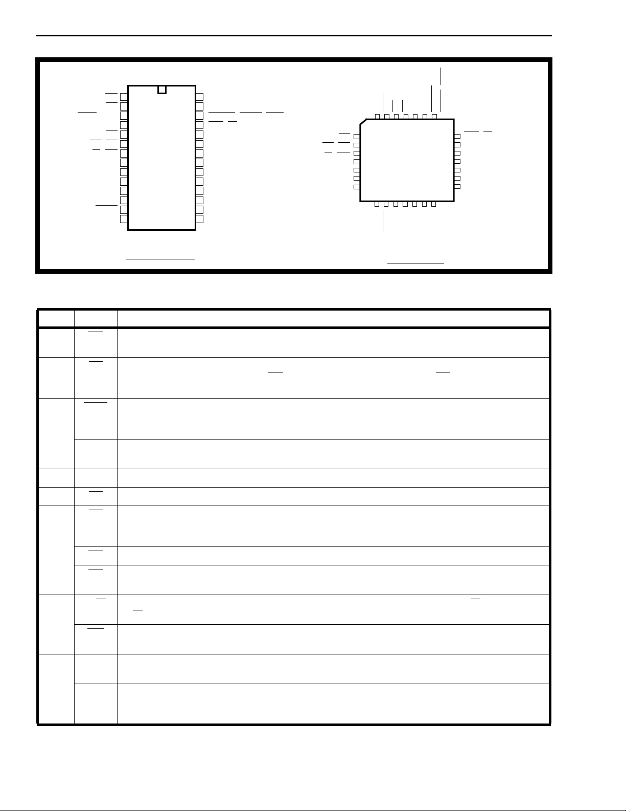
Ordering Information
MT8920BE 28 Pin Plastic DIP
MT8920BP 28 Pin Plastic J-Lead
MT8920BS 28 Pin SOIC
-40°C to 85°C
Description
The ST-BUS Parallel Access Circuit (STPA) provides
a simple interface between Mitel’s ST-BUS and
parallel system environments.
D7-D0
A4-A0
CS
DS, OE
W, WE
R/
DTACK,
BUSY, DCS
IRQ, 24/32
IACK, MS1
STCH
A5,
MMS
Parallel
Port
Interface
Interrupt
Registers
Control
Registers
Tx0
Dual Port Ram
32 X 8
Rx0
Dual Port Ram
32 X 8
Tx1
Dual Port Ram
32 X 8
Address
Generator
V
SS
V
DD
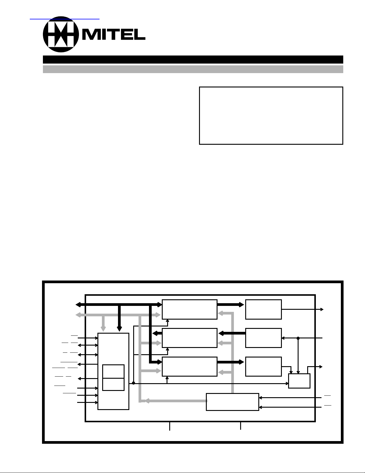
Figure 1 - Functional Block Diagram
Parallelto-serial
Converter
Serial-to-
Parallel
Converter
Parallelto-Serial
Converter
Comp/
MUX
STo0
STi0
STo1
F0i
C4i
3-3
3
MT8920B CMOS
C4i
F0i
IACK, MS1
STi0
CS
DS, OE
W, WE
R/
A0
A1
A2
A3
A4
STCH
A5,
VSS
1
2
3
4
5
6
7
8
9
10
11
12
13
14
28 PIN PDIP/SOIC
28
VDD
27
MMS
26
DTACK, BUSY, DCS
25
IRQ, 24/32
24
STo1
23
STo0
22
D7
21
D6
20
D5
19
D4
18
D3
17
D2
16
D1
15
D0
DS, OE
R/
W, WE
CS
A0
A1
A2
A3
STi0
432
5
6
7
8
9
10
11
1213141516
A4
28 PIN J-LEAD
F0i
IACK, MS1
C4i
1
•
D0D3D2
VSS
STCH
A5,
VDD
28
17
D1
MMS
DTACK,
27
26
18
BUSY, DCS
25
24
23
22
21
20
19
IRQ, 24/32
STo1
STo0
D7
D6
D5
D4
Figure 2 - Pin Connections
Pin Description
Pin # Name Description
1 C4i 4.096 MHz Clock. The ST-BUS timing clock used to establish bit cell boundaries f or the serial
bus.
2 F0i Framing Pulse. A low going pulse used to synchronize the STPA to the 2048 kbit/s ST-BUS
stream. The first falling edge of C4i subsequent to the falling edge of F0i identifies the start of
a frame.
‡
3 IACK Interrupt Acknowledge (Mode 1). This active low input signals that the current b us cycle is
an interrupt vector fetch cycle. Upon receiving this acknowledgement, the STPA will
output a user-programmed vector number on D0 - D7 indicating the source of the interrupt.
MS1 Mode Select 1 (Mode 2,3). This input is used to select the device operating modes. A low
applied to this pin will select mode 3 while a high will select mode 2. (Refer to Table 1.)
4 STi0 ST-BUS Input 0. This is the input for the 2048 kbit/s ST-BUS serial data stream.
5 CS Chip Select. This active low input is used to select the STPA for a parallel access .
6 DS Data Strobe (Mode 1). This active low input indicates to the STPA that v alid data is on the data
bus during a write operation or that the STPA must output valid data on the data bus during a
read operation.
OE Output Enable (Mode 2). This active low input enables the data bus driver outputs.
OE Output Enable (Mode 3). This active low output indicates that the selected device is to be
read and that the data bus is available for data transfer.
7R/WRead/Write (Mode 1,2). This input defines the data bus transfer as a read (R/ W = 1) or a write
(R/W= 0) cycle.
WE Write Enable (Mode 3). This active low output indicates the data on the data bus is to be
written into the selected location of an external device.
8-12 A0-A4 Address Bus (Mode 1,2). These inputs are used to select the internal registers and two-port
memories of the STPA.
A0-A4 Address Bus (Mode 3). These address outputs are generated by the STPA and reflect the
position in internal RAM where the information will be fetched from or stored in. Addresses
generated in this mode are used to access external devices for direct memory transfer.
3-4
Pin Description (continued)
CMOS MT8920B
Pin # Name Description
‡
13 A5 Address Bit A5 (Mode 1). This input is used to extend the address range of the STPA. A5
selects internal registers when high and Tx/Rx RAM’s when low.
A5 Address Bit A5 (Mode 2). This input is used to extend the address range of the STPA. A5
selects Tx0/Rx0 RAM’s when low and Tx1/Rx0 RAM’s when high.
STCH Start of Channel (Mode 3). This signal is a low going pulse which indicates the start of an
ST-BUS channel. The pulse is four bits wide and begins at the start of each valid channel.
14 V
SS
Ground.
15-22 D0-D7 Bidirectional Data Bus. This bus is used to transfer data to or from the STPA during a write
or read operation.
23 STo0 ST-B US Output 0. This output supplies the output ST-BUS 2048 kbit/s serial data stream from
Tx0 two-port RAM.
24 STo1 ST-BUS Output 1. In modes 1 and 2 this output supplies the output ST-BUS 2048 kbit/s serial
data stream from Tx1 two-port RAM. In mode 3, information arriving at STi0 is output here with
one frame delay.
25 IRQ Interrupt Request (Mode 1). This open drain output, when low, indicates when an interrupt
condition has been raised within the STPA.
24/32 24 Channel/32 Channel Select (Mode 2,3). This input is used to select the channel
configuration in modes 2 and 3. A low applied to this pin will select a 24 (T1) channel mode
while a high will select a 32 (CEPT) channel mode.
26 DTACK Data Transfer Acknowledge (Mode 1). This open drain output is supplied by the STPA to
acknowledge the completion of data transfers back to the µP. On a read of the STPA, DTACK
low indicates that the STPA has put valid data on the data bus. On a write, DTACK low
indicates that the STPA has completed latching the µP’s data from the data bus.
BUSY BUSY (Mode 2). This open drain output signals that the controller and the ST-BUS are
accessing the same location in the dual-port RAM’s. It is intended to delay the controller
access until after the ST-BUS completes its access.
DCS Delayed Chip Select (Mode 3). This low going pulse, which is four bit cells long, is active
during the last half of a valid channel. This signal is used to daisy-chain together two STPA’s in
mode 3 that are accessing devices on the same parallel data bus.
27 MMS Master Mode Select (Reset). This Schmitt trigger input selects between either mode 1 (MMS
= 1), or modes 2and 3 (MMS = 0). If MMS is pulsed low in Mode 1 operation the control and
interrupt registers will be reset. (Refer to Table 1.) During power-up, the time constant of the
reset circuit (see Fig. 8) must be a minimum of five times the rise time of the power supply.
28 V
‡ Pin Descriptions pertain to all modes unless otherwise stated.
Mode MMS MS1
1 1 N/A µP
2 0 1 Fast RAM
300 Bus
Power Supply Input. (+5V).
DD
Mode of
Operation
Peripheral
Mode
Mode
Controller
Mode
The STPA provides parallel-to-serial and serial-to-parallel conversions through a
68000-type interface. Two Tx RAMs and one Rx RAM are available along with full
interrupt capability . 32 channel or 24 channel support is availab le . Control Register 1, bit
D
operation.
The STPA provides a fast access interface to Tx0, Tx1 and Rx0 RAMs. This mode is
intended for full parallel support of 24 channel T1/ESF trunks and 32 channel CEPT
trunks. Input
channel operation.
The STPA will synchronously drive the parallel bus using the address generator and
provide all data transfer signals. This mode is intended to support 24 or 32 channel
devices in the absence of a parallel bus controller. Input
operation, input
Function
(RAMCON) = 0 for 32 channel operation and D5 (RAMCON)= 1 for 24 channel
5
24/32 (pin 25) = 0 for 24 channel operation, input 24/32 (pin 25) = 1 for 32
24/32 (pin 25) = 0 for 24 channel
24/32 (pin 25) = 1 for 32 channel operation.
Table 1. STPA Modes of Operation
3-5
MT8920B CMOS
Functional Description
The STPA (ST-BUS Parallel Access) device provides
a simple interface between Mitel’s ST-BUS and
parallel system environments. The ST-BUS is a
synchronous, time division, multiplexed serial
bussing scheme with data streams operating at 2048
kbit/s. The ST-BUS is the primary means of access
for voice, data and control information to Mitel’s
family of digital telecommunications components,
including North American and European digital tr unk
interfaces, ISDN U and S digital line interfaces, filter
codecs, rate adapters, etc. The STPA provides
several modes of operation optimized according to
the type of information being handled.
For interfacing parallel data and control information
to the ST-BUS, such as signalling and link control for
digital trunks, the STPA provides a µP access mode
(Mode 1), and looks like a 68000 type peripheral. In
this mode, the device provides powerful interrupt
features, useful in monitoring digital trunk or line
status (i.e., synchronization, alarms, etc.) or for
setting up message communication links between
microprocessors.
To interface high speed data or multi-channel voice/
data to the ST-BUS for switching or transmission, the
STPA has a high speed synchronous access mode
(Mode 2) and acts like a fast RAM. For voice storage
and forward, bulk data transfer, data buffering and
other similar applications, the STPA has a
controllerless mode (Mode 3) in which it provides
address and control signals to the parallel bus This
is useful for performing direct transfers to the
ST-BUS from external devices such as a RAM buffer.
The STPA is a two port device as shown in the
functional block diagram in Figure 1. The parallel
port provides direct access to three dual port RAM’s,
two transmit and one receive. The address, data and
control busses are used to communicate between
the RAM‘s and a parallel environment.
Two parallel-to-serial converters, and one
serial-to-parallel converter interface the dual port
RAM’s to the ST-BUS port of the STPA. This port
consists of two serial output streams and one serial
input stream operating at 2048 kbit/s. This
configuration of two outputs and one input was
designed to allow a single STPA to form a complete
control interface to Mitel’s digital trunk interfaces
(MT8976, MT8978 and MT8979) which have two
serial input and one serial output control streams.
ST-BUS clocking circuitry, address generator and
various control and interrupt registers complete the
STPA’s functionality.
Modes of Operation
The three basic modes of operation, µP Peripheral
Mode (Mode 1), Fast RAM Mode (Mode 2) and Bus
Controller Mode (Mode 3) are selected using two
external input pins. These inputs are MMS and MS1
and are decoded as shown in Table 1. Whenever
MMS=1 the device resides in Mode 1. In this mode,
MS1 pin is unavailable and is used for a different
function.
When MMS=0, Modes 2 or 3 are selected as
determined by input MS1. If MS1=1, Mode 2 is
selected and if MS1 =0, Mode 3 is selected.
Each of the modes of the STPA provides a different
pinout to ease interfacing requirements of different
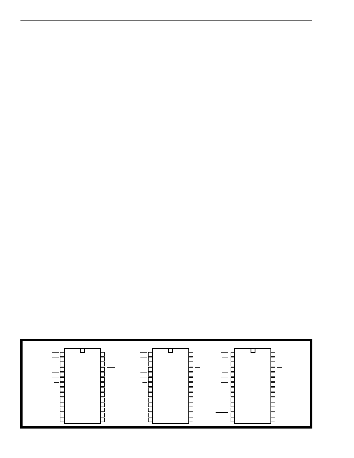
parallel environments. These are shown in Figure 3
below. In µP Peripheral Mode the device uses
interface signals consistent with a 68000-type µP
bus. Mode 2, Fast RAM Mode, uses signals typical
of standard RAM type interfaces. Mode 3 interface
signals are very similiar to Mode 2 signals except
that the address and control signals are supplied as
outputs by the STPA.
3-6
µP Peripheral Mode #1
1
C4i
2
F0i
CS
DS
W
A0
A1
A2
A3
A4
A5
10
11
12
13
14
3
4
5
6
7
8
9
IACK
STi0
R/
VSS
28
27
26
25
24
23
22
21
20
19
18
17
16
15
Mode #2 Bus Controller Mode #3
1
2
3
4
5
6
7
8
9
28
27
26
25
24
23
22
21
20
19
18
17
16
15
VDD
MMS
BUSY
24/32
STo1
STo0
D7
D6
D5
D4
D3
D2
D1
D0
VDD
MMS
DTACK
IRQ
STo1
STo0
D7
D6
D5
D4
D3
D2
D1
D0
C4i
F0i
MS1
STi0
CS
OE
R/
A0
A1
A2
A3
A4
A5
VSS
Fast RAM
W
10
11
12
13
14
Figure 3 - Modes 1, 2, 3 Pin Connections
C4i
F0i
MS1
STi0
CS
OE
WE
A0
A1
A2
A3
A4
STCH
VSS
10
11
12
13
14
1
2
3
4
5
6
7
8
9
28
27
26
25
24
23
22
21
20
19
18
17
16
15
VDD
MMS
DCS
24/32
STo1
STo0
D7
D6
D5
D4
D3
D2
D1
D0

CMOS MT8920B
24/32 Channel Operation
The STPA may be configured to operate as a 32
channel or 24 channel device. This feature, which is
available in all three modes of operation, is
particularly useful in applications involving data
access to CEPT and T1 digital trunk interfaces.
When used as a data interface to Mitel‘s CEPT
digital trunks, the STPA maps the 32 consecutive
bytes of each dual port memory directly to ST-BUS
channels 0-31. This is performed by the address
generator shown in the functional block diagram (see
Figure 1). Figures 4 c & d show the relationship
between relative dual port RAM locations and
corresponding ST-BUS channels, for both input and
output serial streams, when the STPA is configured
as a 32 channel device.
When used as a data interface to Mitel’s T1 trunk
devices, however, only the first 24 consecutive RAM
locations are mapped to 24 of the 32 ST-BUS
channels. This mapping follows a specific pattern
which corresponds with the data streams used by
Mitel‘s T1 products. Instead of a direct correlation
(as in 32 channel operation), the 24 consecutive
RAM locations are mapped to the ST-BUS with every
fourth channel, beginning at channel 0, set to FF
16
(ie. channel 0, 4, 8, 12, 16, 20, 24 and 28). Figures
4 a & b show the relationship between RAM
locations and ST-BUS channel configuration. This
feature allows the STPA to be interfaced directly to
Mitel’s T1 trunk family.
When the STPA is operated in Mode 1, 24 and 32
channel configurations are selected using bit D
(RAMCON) in Control Register 1. D5 = 0 selects 32
channel operation and D5 = 1 selects 24 channel
operation. When the STPA is operated in Modes 2 or
3, however, the channel configuration is done
using input 24/32 (pin 25). When 24/32 = 1 the
device uses all 32 channels and when 24/32 = 0 it
uses 24.
lessened since ST-BUS accesses require only the
last half cycle of C4i of every channel. When
contention does occur, priority is always given to the
ST-BUS access.
The STPA indicates this contention situation in a
different manner for Modes 1 and 2. In Mode 1, the
contention is masked by virtue of the
"handshaking" method used to transfer data on
this 68000-type interface. Data Strobe (DS)
and Data Transfer Acknowledge (DTACK) control
the exchange. If contention should occur the
device will delay returning DTACK and thus stretch
the bus cycle until the µP access can be completed.
In Mode 2, if access is attempted during a
"contention window" the STPA will supply the
BUSY signal to delay the start of the bus cycle. This
“contention window” is defined as shown in Figure
16. The window exists during the last cycle of C4i
clock in each channel timeslot. Although ST-BUS
access is only required during the last half of this
clock period, the “contention window“ exists for the
entire clock period since a parallel access occurring
just prior to an ST-BUS access will not complete
before the ST-BUS access begins. Figure 16 further
shows four possible situations that may occur when
parallel accesses are attempted in and around the
“contention window”. Condition 1 indicates that an
access occurring prior to the contention window but
lasting into the first half of it will complete normally
with no contention arbitration. If the access should
extend past the first half of the contention window
and into the ST-BUS access period, the BUSY signal
will be generated. Conditions 3 and 4 show accesses
occurring inside the contention window. These
5
accesses will result in BUSY becoming active
immediately after the access is initiated and
remaining active as shown in Figure 16.
Access contention is non-existent in Mode 3 since
the parallel bus signals, driven by the STPA, are
synchronized to the ST-BUS clocks.
Dual Port RAMS
Each of the three serial ST-BUS streams is
interfaced to the parallel bus through a 32 byte dual
port RAM. This allows parallel bus accesses to be
performed asynchronously while accesses at the
ST-BUS port are synchronous with ST-BUS clock.
As with any dual port RAM interface between two
asynchronous systems, the possibility of access
contention exists. The STPA minimizes this
occurrence by recognizing contention only when
accesses are performed at the same time for the
same 8-bit cell within the dual port RAM’s.
Furthermore, the probability of contention is
Mode 1 - µP Peripheral Mode
In Mode 1, the STPA operates as an asynchronous
68000-type microprocessor peripheral. All three
dual-port RAMS (Tx0, Tx1, Rx0) are made available
and may be configured as 32 or 24 byte RAM’s. Also
available are the full complement of control and
interrupt registers. The address map for Mode 1 is
shown in Table 2.
The STPA, in Mode 1, uses signals CS, R/W, DS
(Data Strobe), DTACK (Data Acknowledge) IRQ, and
IACK (Interrupt Acknowledge) at the parallel interface.
The pinout of the device is shown in Figure 3.
3-7

MT8920B CMOS
29 30 31
25 26 27 28
21 22 23 24
17 18 19 20
29 30 31
X
X
X
X
X
25 26 27 28
X
21 22 23 24
X
16
17 18 19 20
X
13 14 15 16
X
9 101112
X
5678
X
1234
0
X
0 1 2 3 4 5 6 7 8 9 1011 121314 151617 181920 212223
13 14 15 16
X
9 101112
X
5678
Figure 4 a) RELATIVE Rx RAM ADDRESS vs. ST-BUS CHANNEL - 24 CHANNEL MODE
X
1234
0
X
Figure 4 b) RELATIVE Tx RAM ADDRESS vs. ST-BUS CHANNEL - 24 CHANNEL MODE
0 1 2 3 4 5 6 7 8 9 1011 121314 151617 181920 212223
012345678910111213141516171819202122232425262728293031
012345678910111213141516171819202122232425262728293031
X- unused channels marked X transmit FF
Figure 4 c) RELATIVE Rx RAM ADDRESS vs. ST-BUS CHANNEL - 32 CHANNEL MODE
012345678910111213141516171819202122232425262728293031
Figure 4 d) RELATIVE Tx RAM ADDRESS vs. ST-BUS CHANNEL - 32 CHANNEL MODE
012345678910111213141516171819202122232425262728293031
3-8
STi0
RAM
RELATIVE
LOCATION
STo0
STo1
RAM
RELATIVE
LOCATION
STi0
RAM
RELATIVE
LOCATION
STo0
STo1
RAM
RELATIVE
LOCATION

CMOS MT8920B
ADDRESS BITS REGISTERS
A
A
A
A
A
A
6
5
4
3
2
0
0
0
0
0
•
•
•
•
•
•
•
•
•
•
•
•
•
•
•
0
0
1
1
1
A
1
0
0
0
•
•
•
•
•
•
1
1
X100000 Control Register 1 Control Register 1
X100001 Control Register 2 Control Register 2
X100010 Interrupt Vector Register Interrupt Vector Register
X100100 Interrupt Flag Register 1 X100101 Interrupt Flag Register 2 X100110 Image Register 1 X100111 Image Register 2 X101000 Interrupt Mask Register 1 Interrupt Mask Register 1
X101001 Interrupt Mask Register 2 Interrupt Mask Register 2
X101010 Match Byte Register 1 Match Byte Register 1
X101011 Match Byte Register 2 Match Byte Register 2
X101100Interrupt Channel Address 1 Interrupt Channel Address 1
X101101Interrupt Channel Address 2 Interrupt Channel Address 2
1
0
0
0
0
0
0
•
•
•
•
•
•
•
•
•
•
•
•
•
•
•
•
•
•
•
•
•
1
0
1
1
1
1
1
Table 2. Mode 1 Address Map
NOTES:
X is don’t care
A6 is bit D4 of Control Register 1
READ WRITE
Rx0 - Channel 0
•
•
•
Rx0 - Channel 31
Rx0 - Channel 0
•
•
•
Rx0 - Channel 31
Tx0 - Channel 0
Tx0 - Channel 31
Tx1 - Channel 0
Tx1 - Channel 31
•
•
•
•
•
•
Bit Name Description
7 (Unused)
6 IRQRST Interrupt Reset. This bit, when set high, automatically clears the Interrupt Flag Register
and the Interrupt Image Register without these registers being serviced. This bit
automatically resets to zero after the register clear is completed.
5 RAMCON RAM Configuration. This bit configures Tx0, Tx1 and Rx0 RAMS for 32 or 24 byte
operation. D5 = 0 for 32 channel; D5 = 1 for 24 channel.
4A
6
Address Bit A6. This bit extends the addressing range for access to Tx1 memory.
3 IRQ2MODE Interrupt Source 2 Mode Select. This bit configures the source 2 interrupt generator.
D3 = 0 selects “static” interrupt mode; D3 = 1 selects “dynamic” interrupt mode.
2 IRQ1MODE Interrupt Source 1 Mode Select. This bit configures the source 1 interrupt generator.
D2 = 0 selects “static” interrupt mode; D2 = 1 selects “dynamic” interrupt mode.
1 IRQ2EN Interrupt Source 2 Enable. IRQ2EN = 1 enables interrupts to occur from source 2.
0 IRQ1EN Interrupt Source 1 Enable. IRQ1EN = 1 enables interrupts to occur from source 1.
Table 3. Control Register 1 Bit Definitions
3-9

MT8920B CMOS
Timing information for data transfers on this interface
is shown in Figure 14. The Mode 1 interface is
designed to operate directly with a 68000-type
asynchronous bus but can easily accommodate most
other popular microprocessors as well.
Control Registers
Two control registers allow control of Mode 1
features. Control Register 1 provides bits to select
the type of interrupt, to enable interrupts from two
different and independent sources and to reset the
interrupt registers. Also contained in Control
Register 1 are bits to configure the device for 24 or
32 channel operation and to expand the address
range for convenient access to the second transmit
RAM Tx1. A description of the bit functions in
Control Register 1 is shown in Table 3.
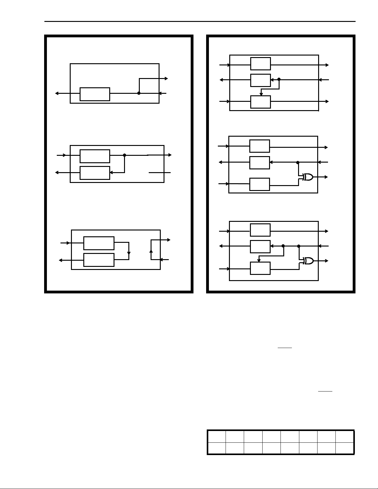
Mode 1 provides various loopback paths and output
configuration options which are controlled by bits in
Control Register 2. Bits D0, D1 of Control Register 2
configure loopbacks using input and output streams
STi0, STo0 as described in Table 4. The input
stream STi0 can be looped back to source the output
stream STo0 as well as receive RAM Rx0. The
transmit RAM Tx0 can be looped to source the
receive RAM Rx0, as well as STo0 and, the transmit
RAM Tx0 can be looped to the receive RAM Rx0
while STi0 sources STo0. The function of these
loopback configurations is shown in Figure 5.
In a similar way, the output STo1 can be reconfigured
for different functionality. Bits D2 and D3 of Control
Register 2 allow STo1 to be sourced, with a one
frame delay via Tx1 from receive stream STi0. STo1
can also output the result of a comparison of the
contents of Tx1 ram with input stream STi0. These
output configurations of STo1 are shown in Figure 6
a and b. Figure 6 c shows the effect of combining
these two features.
Interrupt Registers
Interrupts can be generated in Mode 1 only. Two
channels of the ST-BUS input stream, STi0, can be
selected to provide an interrupt to the system.
Interrupts can be of two types: Static or Dynamic.
Static interrupts are caused when data within a
selected channel matches a given pattern. Dynamic
interrupts occur when bits in a selected channel
change state (1 to 0, 0 to 1 or toggle). Interrupts are
controlled through two identical paths (1 and 2)
consisting of the following registers:
Interrupt Channel Address (1/2): The address
(0-31) of the channel which will generate the
interrupt is stored in this register.
Image Register (1/2): The contents of the
channel causing the interrupt is stored in this
register. Reading this register will clear its contents.
Match Byte Register (1/2): In static mode this
register is used to store the byte which will be
compared with the contents of the selected channel
causing the interrupt.
In dynamic mode, the bits in this register and the
corresponding bit in the Interrupt Mask Register
define the type of dynamic interrupt (i.e., 0 to 1, 1 to
0, toggle). (Refer to Table 5.)
Bit Name Description
7-4 (Unused)
3-2 CONFIG STo1 Output Configuration Bits:
D3D2 = 00- Normal operation. ST-BUS stream from Tx1 is output on STo1 pin.
01- STi0 stream is output on STo1 pin delayed one frame (Figure 6 a).
10- STi0 is compared through XOR (exclusive OR) with ST-BUS stream
from Tx1 and output at STo1 (Figure 6 b).
11- STi0 stream, delayed one frame (via Tx1), is compared (XOR) with the
next frame arriving at STi0 and the result output at STo1 (Figure 6 c).
1-0 LOOPBACK Internal Loopback Configuration Bits:
D1D0 = 00- Normal operation. No internal loops.
01- Loop STi0 to STo0 while still receiving STi0 in Rx0 (Figure 5 a).
10- Loop Tx0 output ST-BUS stream to Rx0 input ST-BUS stream while
outputting Tx0 output to STo0. STi0 is not received (Figure 5 b).
11- Loop Tx0 output ST-BUS stream to Rx0 input ST-BUS stream. Loop
STi0 to STo0 (Figure 5 c).
Table 4. Control Register 2 Bit Definitions
3-10
Control Register 2
Bits D1 = 0, D0 = 1
Control Register 2
= 0, D2 = 1
Bits D
3
CMOS MT8920B
µP
Control Register 2
= 1, D0 = 0
Bits D
1
µP
Control Register 2
Bits D
= 1, D0 = 1
1
µP
Tx0
Rx0
Tx0
Rx0
µP
STo0
STi0Rx0
a)
Control Register 2
= 1, D2 = 0
Bits D
3
STo0
STi0
b)
STo0
STi0
µP
Control Register 2
Bits D3 = 1, D2 = 1
µP
Tx0
Rx0
Tx1
Tx0
Rx0
Tx1
Tx0
Rx0
Tx1
1 Frame Delay
a)
b)
1 Frame Delay
STo0
STi0
STo1
STo0
STi0
STo1
STo0
STi0
STo1
c)
Figure 5 - Loopback Configurations
Interrupt Mask Register (1/2): In static mode the
contents of this register masks bits in the Match Byte
Register that are ’don’t care’ bits
1 - bit masked
0 - bit not masked
In dynamic mode, each bit in this register and the
corresponding bit in the Match Byte Register define
what type of dynamic interrupt is selected. (Refer to
Table 5.)
Interrupt Flag Register (1/2): In static mode
the least significant bit in this register is set to 1 to
flag the corresponding path in which the interrupt
occurs.
In dynamic mode this register sets the bits which
reflect the position of the bits in the corresponding
Interrupt Register which caused the interrupt.
c)
Figure 6 - STo1 Configurations
Interrupt Vector Register
This register shown in Figure 7 is common to both
interrupt paths and stores an 8 bit vector number
which will be output on the data bus when
Interrupt Acknowledge (IACK) is asserted. Bits
labelled V2- V7 are stored by the controlling µP.
Bits IRQ1 and IRQ2 are set by the STPA to indicate
which path caused the interrupt. This creates unique
vectors which are used by the µP to vector to
interrupt service routines. This feature may be
bypassed by simply not asserting IACK during
interrupt acknowledged.
D7 D6 D5 D4 D3 D2 D1 D0
V
V
V
V
V
7
6
5
4
V2IRQ2 IRQ1
3
Figure 7 - Interrupt Vector Registers
3-11

MT8920B CMOS
Interrupt Modes and Servicing
Static Interrupt Mode
A static interrupt is caused when an incoming byte
matches a predefined byte. The incoming byte from
a selected channel is stored in Interrupt Image
Register (1/2) where it is compared with the contents
of the corresponding Match Byte Register. The
result of the comparison of individual bits is masked
by the contents of the Mask Register (1/2) before it
is used to generate an IRQ. After a static interrupt
occurs, information in the Interrupt Image Register is
frozen until the µP performs a read operation on this
register.
When servicing static interrupts assertion of IACK
will cause the contents of the Vector Register, with
the IRQ1 or IRQ2 bit set, to be output on the data
bus. The service routine can subsequently clear IRQ
by reading the Interrupt Image Register.
Alternatively, the IRQRST bit in Control Register 1
can be set to clear the associated interrupt registers.
Static Interrupts are selected using IRQ1MODE and
IRQ2MODE bits in Control Register 1. Interrupts are
then enabled to the IRQ pin with IRQ1EN and
IRQ2EN bits of the same register.
Dynamic Interrupt Mode
A dynamic interrupt is generated by a change of
state of bits in a selected channel. A 0 to 1 transition
or a 1 to 0 transition or a simple change of state from
the previous state (toggle) can be detected. The
type of transition to be detected is selected using two
bits, one from the Match Byte Register (1/2) and one
from the Interrupt Mask Register (1/2), in the
corresponding bit positions. Table 5 shows how the
two registers are programmed.
Match
Byte
Register
bit D
X
Mask
Byte
Register
bit D
X
Transition Type Detected
on Incoming bit D
X
(x = 0 ....7)
Channel Address Register 1 =
(channel 4 of STi0 selected)
Match Byte Register 1 =
Interrupt Mask Register 1 =
(When bit D3 toggles 0 to 1)
D7D6D5D4D3D2D1D
00000100
00000000
00001000
0
Dynamic interrupts from interrupt path 1 would then
be enabled using the Control Register 1.
Control Register 1 =
00000101
This would cause interrupt 1 path to be enabled
while interrupt 2 path is disabled.
As with static interrupts, upon serving a dynamic
interrupt, assertion of IACK will cause the contents
of the Vector Register, with the appropriate path bit
set, to be output on the data bus. The information
contained in the channel is frozen in the Interrupt
Image Register. To clear a dynamic interrupt,
however, the µP must read the Interrupt Flag
Register of the path responsible for the interrupt to
determine which bit caused the interrupt. The bit in
the corresponding position will be set to 1 and
reading this register will clear its contents.
Alternatively, as with static interrupts, the IRQRST bit
in Control Register 1 can be set to clear the Image
Interrupt Register, Flag Register and path bits in the
Vector Register.
Dynamic Interrupts are selected using IRQ1MODE
and IRQ2MODE bits in Control Register 1 and are
enabled using IRQ1EN and IRQ2EN in the same
register.
MMS Pin Reset
The STPA can be RESET in Mode 1 using the MMS
pin (27). Applying a low pulse (0V) to MMS after
power is applied to the device will reset all control
and interrupt registers to 0016. This can be
accomplished on power up with a simple R-C circuit
as shown in Figure 8.
0
0
1
1
0
1
0
1
Mask Bit D
X
0 to 1 transition
1 to 0 transition
Toggle
Table 5 - Dynamic Interrupt Types
For example, the following steps are required to
generate an interrupt when bit D3 of channel 4
changes state from 0 to 1 (all other bits are masked):
3-12
V
DD
R
MMS
C
STPA
27
Figure 8 - MMS Reset Function

CMOS MT8920B
Mode 2 - Fast RAM Mode
Mode 2 operates as a high speed dual port RAM
interface to the ST-BUS. Only the two transmit
RAM’s, Tx0 and Tx1, and the receive RAM, Rx0 are
active in this mode (i.e., control registers and
interrupt registers are inactive).
The main feature of this mode is fast access to the
dual-port RAM’s. Fast access allows high-speed
controllers to use this device as a data interface to
T1 and CEPT digital links. Timing information is
shown in Figure 15.
Mode 2 can also support 24 channel and 32 channel
operation. The channel configuration is selected
using 24/32 pin. When 24/32=0 the device operates
in 24 channel mode and when 24/32=1, it operates in
32 channel mode.
The physical interface in this mode resembles that of
a simple RAM device. The signals used to read
and write the device are CS, OE, R/ W. The pinout of
the STPA in this mode is shown in Figure 3. Address
decoding for Tx0, Tx1, Rx0 is shown in Table 6.
Contention can arise for access to the dual port
RAMS. The occurrence of this is minimized since
the ST-BUS serial-to-parallel and parallel-to-serial
converters require RAM access for only 1/32 of
a channel time (i.e., last half cycle of C4i for
each channel). For contention to occur the high
speed controller must access the same RAM
location as that of the ST-BUS. For a parallel read
operation this corresponds to the current ST-BUS
channel and for a write operation, the next ST-BUS
channel. Access contention in Mode 2 is arbitrated
with the BUSY signal. BUSY is intended to hold
off any parallel access cycle until it again goes
inactive. Figure 16 shows how the access is
arbitrated for accesses near the contention window.
Applications using high speed access can easily
avoid generating BUSY by co-ordinating channel
reads and writes with framing and channel boundary
information.
Mode 3 - Parallel Bus Controller
In this mode the STPA outputs all necessary signals
required to drive devices attached to the parallel
port. The STPA can be used to dr ive devices such
as RAM’s, FIFO’s, latches, A/D and D/A converters,
and CODECS, directly from the ST-BUS without an
intervening µP. As with the other modes, Mode 3 can
operate from 32 channels or 24 channels by
connecting 24/32 high or low, respectively. This
allows devices to be driven remotely via a T1 or
CEPT digital trunk link when used with Mitel’s trunk
products.
Referring to Figure 1, the Address Generator block
generates and drives the external address lines
A4-A0. The STPA also generates OE (output
enable) and WE (write enable) to facilitate data
transfers from Rx0 RAM and to Tx0 RAM. Tx1 RAM
is unavailable in this mode.
The STPA, in Mode 3, generates external addresses
in a particular sequence that minimizes throughput
delay through the device. When channel N is
present on the ST-BUS, the STPA generates address
N+1 on the address bus and asserts OE to output
data from an external device and latch it into the
STPA. During the same channel N, the STPA
will generate address N-1 with WE asserted to
write from the STPA to an external device. Timing for
Mode 3 transfers is shown in Figure 17. All parallel
bus signals are synchronized to the ST- BUS clock.
The device must be selected using CS in order for
the parallel bus drivers to be enabled. CS should
remain active for four ST-BUS bit periods (8 x C4i
cycles) since a read and a write operation require 2
bit periods each. The STPA generates a signal STCH
(start of channel) which becomes active at the start
of each channel and remains active for 1/2 of the
channel time (Figure 18). This signal may be
ADDRESS BITS REGISTERS
A
A
5
0
•
•
•
0
1
•
•
•
1
A
4
0
•
•
•
1
0
•
•
•
1
A
3
0
•
•
•
1
0
•
•
•
1
A
2
0
•
•
•
1
0
•
•
•
1
A
1
0
•
•
•
1
0
•
•
•
1
0
0
•
•
•
1
0
•
•
•
1
READ WRITE
Rx0 - Channel 0
•
•
•
Rx0 - Channel 31
Rx0 - Channel 0
•
•
•
Rx0 - Channel 31
Tx0 - Channel 0
•
•
•
Tx0 - Channel 31
Tx1 - Channel 0
•
•
•
Tx1 - Channel 31
Table 6. Mode 2 Address Map
3-13

MT8920B CMOS
connected directly to CS to enable the device
appropriately.
Common Bus
CS STCH
OE
WE
A0
A1
A2
A3
A4
MMS MS1
00 1
OE
WE
A0
A1
A2
A3
A4
CS DCS
MMS MS1
00 1
24/32
24/32
STi0
STo0
STi0
STo0
Figure 9 - "Daisy-chained" STPA’s in 32 Channel
Parallel Bus Controller Mode (Mode 3)
In order to facilitate efficient use of the parallel bus
another signal, similar to STCH, is supplied by the
STPA. Delayed Chip Select (DCS) becomes active
for the last half of each channel (Figure 19). This
may be connected to a second STPA, residing on the
same physical parallel bus, enabling it to perform its
read/write operations in the second half of each
channel. This allows a large number of devices,
connected on a common bus, to be driven by two
ST-BUS streams. Figure 9 shows how this "daisy
chaining" of STPA’s is implemented while Figure 10
illustrates the timing on the shared parallel bus.
Applications
Parallel PBX to Digital Trunk Interface
The STPA is an ideal component for interfacing
parallel PBX environments to Mitel’s family of digital
trunk devices.
Figure 11 shows a typical interface for both T1/ESF
and CRC-4 CEPT digital trunks to a system utilizing
a parallel bus architecture. Both the MH89760B
T1/ESF and the MH89790B CRC-4 CEPT trunk
modules are shown interfaced to a parallel bus
structure using two STPAs operating in modes 1 and
2.
The first STPA operating in mode 2 (MMS=0,
MS1=1, 24/32=0), routes data and/or voice
information between the parallel telecom bus and the
T1 or CEPT link via DSTi and DSTo. The second
STPA, operating in mode 1 (MMS=1) provides
access from the signalling and link control bus to the
MH89760B or MH89790B status and control
channels. All signalling and link functions may be
controlled easily through the STPA transmit RAM’s
Tx0, Tx1, while status information is read at receive
RAM Rx0. In addition, interrupts can be set up to
notify the system in case of slips, loss of sync,
alarms, violations, etc.
3-14
ST-BUS
C4i
Address
OE
WE
Data Bus
STCH
DCS
CHANNEL N
BIT 7 BIT 6 BIT 5 BIT 4 BIT 3 BIT 2 BIT 1 BIT 0
N + 1 N - 1 N + 1 N - 1
IN OUT IN OUT
Figure 10 - Timing Relationship for Mode 3 Daisy Chaining

CMOS MT8920B
†
Tx
TxA
EQU
Line
TxB
DIP
Switch
MH89760B/790B
MT8977/79
DSTi
DSTo
Driver
CSTi0
MH89761*
CSTo
CSTi1
Rx
RxA
F0i
Line
Receiver
RxB
†
C2i
C1.5i
RxD
)
††
(E2i
†
E1.5i
E8Ko
Clock
Extractor
†
MT8940
12.355
MHz Osc.
†
C1.5o†F0i
C2o
16.388
F0b
C4b
MHz Osc.
C8Kb
(Mode 2)
MT8920B
STo0
7
-D
0
D
HIGH
STi0
STo1
5
-A
0
A
SPEED
PARALLEL
C4i
CS
R/WOE
BUS
TELECOM
F0i
24/32
MMS MS1
†
††
+5V
+5V
(Mode 1)
MT8920B
-D
D
7
0
STo0
-A
A
STi0
STo1
5
0
CS
R/WDTACK
DS
BUS
AND LINK
CONTROL
SIGNALLING
C4i
F0i
IRQ
IACK
MMS
+5V
Figure 11 - Typical T1-ESF / CRC-4 CEPT Digital Trunk Configuration
NOTES:
† Signals applicable to T1-ESF applications using MT8977 and MH89760B
†† Signals applicable to CRC-4 CEPT applications using MT8979 and MH89790B
* Equalizer MH89761 available for T1/ESF applications
3-15

MT8920B CMOS
Digital Signal Processor to ST-BUS Interface
Mode 2 allows many high speed devices to be easily
connected to the ST-BUS. Figure 12 shows a
TMS32020 digital signal processor interfaced to the
ST-BUS through the STPA. This simple interface
allows complex functions to be implemented in such
systems as PBX’s and computer systems. Some of
the possible functions include:
- Digital Filtering
- Voice Conferencing
- Speech/Data Compression
- Encryption
- Tone Detection and Generation
- Frequency Spectrum Analysis
- Image Processing
- µ-Law to A-Law Conversion
- Echo Cancellation
- Modulation
- Speech Synthesis and Recognition
TMS32020
A8-A0
D7-D0
STRB
READY
DS
RW
MSC
A9
A8
A7
A6
74HCT
138
E2
E1
A
B
C
MT8920B
CS
A5-A0
D7-D0
OE
WE
MMS MS1
STo0
STi0
STo1
24/32
+5V +5V
3-16
Figure 12 - ST-BUS to DSP Interface

CMOS MT8920B
Connecting the STPA to a shared ST-BUS Line
The STPA’s STo0 and STo1 outputs cannot be
directly forced into a high impedance state.
However, with some external logic, the STo0 output
can be buffered by a three-state device, controlled by
the STo1 output. This application is only possible if
the Tx1 RAM and associated STo1 output are not
required for some other purpose.
Figure 13 shows an external buffer U1 controlled by
the STo1 output and an external Output Data Enable
(ODE) signal. When FF (hex) is written to the Tx1
RAM, the corresponding STo1 output channel goes
to logic high. This signal, AND-ed together with a
logic high at ODE, enables U1, resulting in the STo0
signal transparently passed to the output of U1.
When 00 (hex) is written to the Tx1 RAM, the STo1
output goes logic low. This disables U1, resulting in
a high impedance state at the output of U1,
corresponding to the selected channel.
This method of three-state buffering permits output
control on a per-channel or per-bit basis.
The ODE input is used to enable the ST-BUS outputs
after all ST-BUS devices are properly configured by
software. This eliminates the possibility of
contention on the ST-BUS lines during the power-up
state.
Parallel Port
Parallel Port
ODE
STo0
MT8920B
STo1
ODE
STi0
STi1
STi7 STo7
STo0
STo1
MT8980
74HC00
74HC125
U2
U1
ST-BUS
Figure 13 - Connecting STPA to a Common ST-BUS Line
3-17

MT8920B CMOS
Absolute Maximum Ratings* - Voltages are with respect to ground (V
) unless otherwise stated.
SS
Parameter Symbol Min Max Units
1 Supply Voltage V
DD
-0.3 7.0 V
2 Voltage on any I/O pin -0.3 VDD + 0.3 V
3 Current on any I/O pin I
4 Storage Temperature T
5 Package Power Dissipation Plastic P
* Exceeding these values may cause permanent damage. Functional operation under these conditions is not implied.
Recommended Operating Conditions - Voltages are with respect to ground (V
Characteristics Sym Min Typ
1 Supply Voltage V
2 Input High Voltage V
3 Input Low Voltage V
4 Operating Temperature T
5 Operating Clock Frequency f
‡ Typical figures are at 25°C and are for design aid only: not guaranteed and not subject to production testing.
4.75 5.0 5.25 V
DD
IH
IL
A
CK
2.4 V
0 0.4 V for 400mV noise margin
-40 25 85 °C
I/O
ST
D
‡
-55 125 °C
SS
Max Units Test Conditions
DD
V for 400mV noise margin
4.096 MHz
) unless otherwise stated.
±25 mA
600 mW
DC Electrical Characteristics - Voltages are with respect to ground (V
Characteristics Sym Min Typ
1 Supply Current Static
Dynamic
2 Input High Voltage V
3 Input Low Voltage V
4 Input Leakage Current I
I
CCS
I
CCD
10
510
IH
IL
Z
2.0 V
) unless otherwise stated.
SS
‡
Max Units Test Conditions
µAmAoutputs unloaded
@fCK = 4.096 MHz
0.8 V
±10 µAVDD=5.25V,
VIN=VSSto V
5 Input capacitance C
6 Schmitt trigger input high (MMS) V
7 Schmitt trigger input low (MMS) V
8 Schmitt trigger hysteresis (MMS) V
9 Output high current (except IRQ) I
10 Output low current (except IRQ) I
11 IRQ, DTACK, BUSY Sink Current I
12 Tristate Leakage A4-A0, OE, WE
I
IN
T+
OH
OL
OL
OZ
3.8 3.0 V
T-
0.8 1.0 V
H
2.0 1.0 V
10 15 mA VOH= 2.4V, VDD = 4.75V
510 mAVOL = 0.4V, VDD = 4.75V
10 15 mA VOL = 0.4V, VDD = 4.75V
±1 ±10 µAVDD = 5.25V
(mode 3)
13 Open drain off-state current
I
OFF
±1 ±20 µAVDD = 5.25V
IRQ, DTACK, BUSY
14 Output capacitance C
‡ Typical figures are at 25°C and are for design aid only: not guaranteed and not subject to production testing.
O
10 pF
V
V
15 pF
= VSS to V
OUT
= V
OUT
DD
DD
DD
3-18

CMOS MT8920B
AC Electrical Characteristics†- Mode 1 Parallel Bus Timing (see Fig. 14)
(VCC=5.0V ±5%,TA=-40 to 85°C)
Characteristics Sym Min Typ
††
††
††
t
ARDS
t
RWDS
t
RDS
RD
0ns
20 ns
1,2
t
cwmtCLK
t
cwm
1 Address to DS (CS) Low
2R/W to DS (CS) Low
3 DS (CS) Low to DTACK Low
4 Valid Data to DTACK Low (Read) t
-30
5 DS High to DTACK High t
6 DS High to Data High Imped.(Read) t
7 DS High to CS High t
8 Data Hold Time (Write) t
9 Input Data Valid after DS t
10 Address Hold Time
† Timing is over recommended temperature & power supply voltages.
‡ Typical figures are at 25°C, VDD=5V, t
testing.
††The cycle is initiated by the falling edge ofCS orDS , whichever occurs last. Timing is relative to the last falling edge which initiates the cycle.
(1) t
is equal to tCH or tCL whichever is smaller (some ST-BUS compatible transceivers may generate C4 clock having t
cwm
or t
(2) Worst case access when memory contention occurs.
CLmin
=70ns.
††
=244 ns, tCH=tCL=122 ns and are for design aid only: not guaranteed and not subject to production
CLK
DAR
DHZ
CSH
DHT
DST
t
ADHT
045ns
0ns
0ns
50 ns
‡
Max Units Test Conditions
2*t
CLK
65 ns
t
cwm
ns
ns
ns
Load C
Load A, CL=130pF, RL=740Ω
Load C, CL=50pF
Load A, CL=130pF, RL=740Ω
-30
CHmin
=70ns
A0 - A5
CS (IACK†)
R/W
DS
DTACK
D0 - D7
t
RWDS
t
ARDS
t
DST
t
ADHT
t
RDS
t
CSH
t
DAR
t
RD
DATA OUT
t
DHT
t
DHZ
D0 - D7
DATA IN
Figure 14 - Mode 1 Parallel Bus Timing
† During Interrupt Acknowledge cycle IACK replaces CS. R/W must remain high.
3-19

MT8920B CMOS
AC Electrical Characteristics† - Mode 2 Parallel Bus Timing - (see Figures 15 and 16)
(VCC=5.0V ±5%,TA=-40 to 85°C)
Characteristics Sym Min Typ
‡
Max Units Test Conditions
1 OE Low to Valid Data t
2 Address Access Time t
3 CS Low to Valid Data t
4 Output Disable t
5 Address Setup Time t
6 Data Setup Time t
7 Data Hold Time t
8 Address Hold Time t
9 Write Pulse Width t
10 OE, R/W High to C4i High t
11 OE, R/W Low to C4i Low t
12 C4i High to Busy Low t
13 C4i Low to Busy High t
14 OE, R/W High to Busy Low t
† Timing is over recommended temperature & power supply voltages.
‡ Typical figures are at 25°C, VDD=5V, t
testing.
=244 ns, tCH=tCL=122 ns and are for design aid only: not guaranteed and not subject to production
CLK
EVD
AA
CSD
OHZ
ASF
DST
DHT
AH
WP
EC4H
EC4L
C4BL
C4BH
EBL
20 ns
30 ns
5ns
50 ns
50 ns
60 ns
120 ns
60 ns
50 ns
-10 ns
10 ns
50 ns
50 ns
40 ns
Load A, CL=130pF, RL=740Ω
Load A, CL=130pF, RL= 740Ω
Load A, CL=130pF, RL=740Ω
Load A, CL=130pF, RL=740Ω
Load C
Load C
Load C
A0 - A5
CS
OE
R/W
D0 - D7
t
AH
t
ASF
t
WP
t
OHZ
t
EVD
t
CSD
t
AA
t
Figure 15 - Mode 2 Timing Diagram (No Contention)
DST
t
DHT
DATA INDATA OUT
3-20

CMOS MT8920B
C4i
A0 - A5
CS
CONDITION 1:
OE, R/W
BUSY
CHANNEL N - BIT 0
CHANNEL (N + 1) - BIT 7
ST-BUS ACCESS
CONTENTION WINDOW
READ ADDRESS N or WRITE ADDRESS (N + 1)
(N matches incoming
ST-BUS channel)
Access begins before contention window and finishes before ST-BUS access - No contention.
t
EC4H
CONDITION 2:
OE, R/W
BUSY
CONDITION 3:
OE, R/W
BUSY
CONDITION 4:
OE, R/W
BUSY
Access begins before contention window and continues into ST-BUS access.
t
EC4L
t
C4BL
Access begins within contention window but before ST-BUS access.
t
EC4L
t
t
EBL
C4BH
Access begins during ST-BUS access
t
EBL
t
C4BH
t
C4BH
Figure 16 - Mode 2 Access Contention Resolution
3-21

MT8920B CMOS
AC Electrical Characteristics† - Mode 3 Timing (see Fig.17, 18 and 19)
((VCC=5.0V ±5%,TA=-40 to 85°C)
Characteristics Sym Min Typ
‡
Max Units Test Conditions
1 CS to OE, WE, Address Enabled t
2 C4i Low to Address Change t
3 CS to OE, WE, Address Disabled t
4 C4i Low to Output Enable Low t
5 C4i Low to Output Enable High t
6 OE, WE, Pulse Width t
7 C4i Low to Write Enable Low t
8 C4i Low to Write Enable High t
9 Read Data Valid from OE t
10 Read Data Hold Time t
11 Write Data Setup Time t
12 Write Data Hold Time t
13 C4i Transition to STCH, DCS Trans. t
14 STCH Pulse Width t
15 DCS Pulse Width t
† Timing is over recommended temperature & power supply voltages.
‡ Typical figures are at 25°C, VDD=5V,t
testing.
=244ns, tCH=tCL=122ns and are for design aid only: not guaranteed and not subject to production
CLK
ZR
ACS
RZ
OED
OEH
ENPW
WED
WEH
RST
RHT
WST
WHT
STC
SCPW
CSPW
0ns
70 100 ns
70 100 ns
50 ns
110 ns
50 ns
75 ns
75 ns
2*t
CLK
75 ns
75 ns
(2*t
CLK
)
-60
120 ns
1830 ns
1830 ns
Load A, CL = 130pF, RL = 740Ω
Load A, CL = 130pF, RL = 740Ω
Load A, CL = 130pF, RL = 740Ω
Load A, CL = 130pF, RL = 740Ω
Load A, CL = 130pF, RL = 740Ω
Load A, CL = 130pF, RL = 740Ω
ns
Load A, CL = 130pF, RL = 740Ω
Load A, CL = 130pF, RL = 740Ω
ns
Load A, CL = 130pF, RL = 740Ω
Load A, CL = 130pF, RL = 740Ω
Load A, CL = 70pF, RL = 1.22KΩ
Load A, CL = 70pF, RL = 1.22KΩ
Load A, CL = 70pF, RL = 1.22KΩ
C4i
A4 - A0
OE
WE
D7 - D0
CS
CHANNEL N
BIT 7 (BIT 3) BIT 6 (BIT 2) BIT 5 (BIT 1) BIT 4 (BIT 0)
t
ACS
N + 1 N - 1
t
OED
t
ENPW
t
RST
DATA IN DATA OUT
t
ZR
t
OEH
t
RHT
t
WST
t
WED
t
ENPW
t
WEH
t
WHT
t
RZ
3-22
Figure 17 - Mode 3 Timing Diagram

CMOS MT8920B
CHANNEL N-1
C4i
STCH
CHANNEL N
BIT 0 BIT 7 BIT 6 BIT 5 BIT 4
t
STC
t
SCPW
t
STC
Figure 18 - Mode 3 STCH Timing Diagram
CHANNEL N CHANNEL
BIT 4 BIT 3 BIT 2 BIT 1 BIT 0
C4i
STCH
DCS
t
STC
t
CSPW
Figure 19 - Mode 3 DCS Timing Diagram
t
STC
N+1
3-23

MT8920B CMOS
AC Electrical Characteristics† - ST-BUS Timing (see Figure 20)
(VCC = 5.0V ± 5%, TA = -40 to 85°C)
Characteristics Sym Min Typ
‡
Max Units Test Conditions
1 Clock C4i Period t
2 Clock C4i Period High t
3 Clock C4i Period Low t
4 C4i Rise Time t
5 C4i Fall Time t
6 Frame Pulse Setup Time t
7 Frame Pulse Hold Time t
8 STo0/1 Delay from C4i t
9 STi0 Setup Time t
10 STi0 Hold Time t
† Timing is over recommended temperature & power supply voltages.
‡ Typical figures are at 25°C, VDD=5V and are for design aid only: not guaranteed and not subject to production testing.
CLK
CH
CL
R
F
FPS
FPH
SOD
STS
STH
70 122 ns
70 122 ns
20 ns
20 ns
20 ns
35 ns
244 ns
20 ns
12 ns
100 ns Load B
C4i
F0i
STo0
STo1
STi0
t
FPS
t
SOD
t
t
CLK
FPH
Bit Cell
t
STStSTH
t
CL
t
CH
t
R
t
F
3-24
Figure 20 - ST-BUS Timing Diagram

125 µs
CMOS MT8920B
CHANNEL31CHANNEL
INPUTS
OUTPUTS
2.0 V
0.8 V
2.0 V
0.8 V
0
Bit D
7
on
Data Bus
CHANNEL30CHANNEL31CHANNEL
(8/2.048) µs
BIT 7 BIT 6 BIT 5 BIT 4 BIT 3 BIT 2 BIT 1 BIT 0
Figure 21 - Format of 2048 kbit/s ST-BUS Streams
0
Bit D
0
on
Data Bus
Figure 22 - Waveform Test Point Reference
V
DD
V
R
L
C
L
6.0k
IN4148
LOAD A
CL=150pF
=130pF
C
L
LOAD B LOAD C
DD
500Ω
Figure 23 - Test Load Circuits
3-25

MT8920B CMOS
Notes:
3-26

Pin 1
Package Outlines
E
A
A
1
16-Pin 18-Pin 20-Pin 24-Pin 28-Pin
DIM
Min Max Min Max Min Max
A 0.093
A
B 0.013
C 0.009
D 0.398
E 0.291
e 0.050 BSC
H 0.394
L 0.016
(2.35)
1
0.004
(0.10)
(0.33)
(0.231)
(10.1)
(7.40)
(1.27 BSC)
(10.00)
(0.40)
0.104
(2.65)
0.012
(0.30)
0.020
(0.51)
0.013
(0.318)
0.413
(10.5)
0.299
(7.40)
0.419
(10.65)
0.050
(1.27)
D
0.093
(2.35)
0.004
(0.10)
0.013
(0.33)
0.009
(0.231)
0.447
(11.35)
0.291
(7.40)
0.050 BSC
(1.27 BSC)
0.394
(10.00)
0.016
(0.40)
L
e
4 mils (lead coplanarity)
Notes:
1) Not to scale
2) Dimensions in inches
3) (Dimensions in millimeters)
4) A & B Maximum dimensions include allowable mold flash
B
0.104
(2.65)
0.012
(0.30)
0.030
(0.51)
0.013
(0.318)
0.4625
(11.75)
0.299
(7.40)
0.419
(10.65)
0.050
(1.27)
0.093
(2.35)
0.004
(0.10)
0.013
(0.33)
0.009
(0.231)
0.496
(12.60)
0.291
(7.40)
0.050 BSC
(1.27 BSC)
0.394
(10.00)
0.016
(0.40)
0.104
(2.65)
0.012
(0.30)
0.020
(0.51)
0.013
(0.318)
0.512
(13.00)
0.299
(7.40)
0.419
(10.65)
0.050
(1.27)
Lead SOIC Package - S Suffix
C
H
L
Min Max Min Max
0.093
(2.35)
0.004
(0.10)
0.013
(0.33)
0.009
(0.231)
0.5985
(15.2)
0.291
(7.40)
0.050 BSC
(1.27 BSC)
0.394
(10.00)
0.016
(0.40)
0.104
(2.65)
0.012
(0.30)
0.020
(0.51)
0.013
(0.318)
0.614
(15.6)
0.299
(7.40)
0.419
(10.65)
0.050
(1.27)
0.093
(2.35)
0.004
(0.10)
0.013
(0.33)
0.009
(0.231)
0.697
(17.7)
0.291
(7.40)
0.050 BSC
(1.27 BSC)
0.394
(10.00)
0.016
(0.40)
(0.318)
0.7125
(10.65)
0.104
(2.65)
0.012
(0.30)
0.020
(0.51)
0.013
(18.1)
0.299
(7.40)
0.419
0.050
(1.27)
NOTES: 1. Controlling dimensions in parenthesis ( ) are in millimeters.
2. Converted inch dimensions are not necessarily exact.
General-7

Package Outlines
F
D
1
D
H
E
E
1
e: (lead coplanarity)
A
1
I
E
2
Notes:
1) Not to scale
2) Dimensions in inches
3) (Dimensions in millimeters)
4) For D & E add for allowable Mold Protrusion 0.010"
A
G
D
2
Dim
A
A
D/E
D1/E
D2/E
e
F
G
H
I
20-Pin 28-Pin 44-Pin 68-Pin 84-Pin
Min Max Min Max Min Max Min Max Min Max
0.165
(4.20)
0.090
1
(2.29)
0.385
(9.78)
0.350
1
(8.890)
0.290
2
(7.37)
0.026
(0.661)
0.013
(0.331)
0.020
(0.51)
0.180
(4.57)
0.120
(3.04)
0.395
(10.03)
0.356
(9.042)
0.330
(8.38)
0 0.004 0 0.004 0 0.004 0 0.004 0 0.004
0.032
(0.812)
0.021
(0.533)
0.050 BSC
(1.27 BSC)
0.165
(4.20)
0.090
(2.29)
0.485
(12.32)
0.450
(11.430)
0.390
(9.91)
0.026
(0.661)
0.013
(0.331)
0.050 BSC
(1.27 BSC)
0.020
(0.51)
0.180
(4.57)
0.120
(3.04)
0.495
(12.57)
0.456
(11.582)
0.430
(10.92)
0.032
(0.812)
0.021
(0.533)
0.165
(4.20)
0.090
(2.29)
0.685
(17.40)
0.650
(16.510)
0.590
(14.99)
0.026
(0.661)
0.013
(0.331)
0.050 BSC
(1.27 BSC)
0.020
(0.51)
0.180
(4.57)
0.120
(3.04)
0.695
(17.65)
0.656
(16.662)
0.630
(16.00)
0.032
(0.812)
0.021
(0.533)
0.165
(4.20)
0.090
(2.29)
0.985
(25.02)
0.950
(24.130)
0.890
(22.61)
0.026
(0.661)
0.013
(0.331)
0.050 BSC
(1.27 BSC)
0.020
(0.51)
0.200
(5.08)
0.130
(3.30)
0.995
(25.27)
0.958
(24.333)
0.930
(23.62)
0.032
(0.812)
0.021
(0.533)
(30.10)
(29.210)
(27.69)
(0.661)
(0.331)
0.165
(4.20)
0.090
(2.29)
1.185
1.150
1.090
0.026
0.013
0.050 BSC
(1.27 BSC)
0.020
(0.51)
0.200
(5.08)
0.130
(3.30)
1.195
(30.35)
1.158
(29.413)
1.130
(28.70)
0.032
(0.812)
0.021
(0.533)
General-10
Plastic J-Lead Chip Carrier - P-Suffix

Package Outlines
E
1
D
32
n-2 n-1 n
1
E
L
Notes:
1) Not to scale
2) Dimensions in inches
3) (Dimensions in millimeters)
A
b
D
1
e
2
b
A
2
Plastic Dual-In-Line Packages (PDIP) - E Suffix
8-Pin 16-Pin 18-Pin 20-Pin
DIM
Plastic Plastic Plastic Plastic
Min Max Min Max Min Max Min Max
A
A
2
b
b
2
C
D
D
1
E
E
1
e
e
A
L
e
B
e
C
NOTE: Controlling dimensions in parenthesis ( ) are in millimeters.
0.115 (2.92) 0.195 (4.95) 0.115 (2.92) 0.195 (4.95) 0.115 (2.92) 0.195 (4.95) 0.115 (2.92) 0.195 (4.95)
0.014 (0.356) 0.022 (0.558) 0.014 (0.356) 0.022 (0.558) 0.014 (0.356) 0.022 (0.558) 0.014 (0.356) 0.022 (0.558)
0.045 (1.14) 0.070 (1.77) 0.045 (1.14) 0.070 (1.77) 0.045 (1.14) 0.070 (1.77) 0.045 (1.14) 0.070 (1.77)
0.008
(0.203)
0.355 (9.02) 0.400 (10.16) 0.780 (19.81) 0.800 (20.32) 0.880 (22.35) 0.920 (23.37) 0.980 (24.89) 1.060 (26.9)
0.005 (0.13) 0.005 (0.13) 0.005 (0.13) 0.005 (0.13)
0.300 (7.62) 0.325 (8.26) 0.300 (7.62) 0.325 (8.26) 0.300 (7.62) 0.325 (8.26) 0.300 (7.62) 0.325 (8.26)
0.240 (6.10) 0.280 (7.11) 0.240 (6.10) 0.280 (7.11) 0.240 (6.10) 0.280 (7.11) 0.240 (6.10) 0.280 (7.11)
0.100 BSC (2.54) 0.100 BSC (2.54) 0.100 BSC (2.54) 0.100 BSC (2.54)
0.300 BSC (7.62) 0.300 BSC (7.62) 0.300 BSC (7.62) 0.300 BSC (7.62)
0.115 (2.92) 0.150 (3.81) 0.115 (2.92) 0.150 (3.81) 0.115 (2.92) 0.150 (3.81) 0.115 (2.92) 0.150 (3.81)
0 0.060 (1.52) 0 0.060 (1.52) 0 0.060 (1.52) 0 0.060 (1.52)
0.210 (5.33) 0.210 (5.33) 0.210 (5.33) 0.210 (5.33)
0.014 (0.356) 0.008 (0.203) 0.014(0.356) 0.008 (0.203) 0.014 (0.356) 0.008 (0.203) 0.014 (0.356)
0.430 (10.92) 0.430 (10.92) 0.430 (10.92) 0.430 (10.92)
C
e
A
e
B
e
C
General-8

E
1
L
Notes:
1) Not to scale
2) Dimensions in inches
3) (Dimensions in millimeters)
Package Outlines
32
1
E
n-2 n-1 n
D
A
b
D
1
e
2
b
A
2
C
e
A
e
B
Plastic Dual-In-Line Packages (PDIP) - E Suffix
α
DIM
A
A
b
b
2
C
D
D
E
E
E
E
e
e
A
e
A
e
B
L
α
22-Pin 24-Pin 28-Pin 40-Pin
Plastic Plastic Plastic Plastic
Min Max Min Max Min Max Min Max
0.210 (5.33) 0.250 (6.35) 0.250 (6.35) 0.250 (6.35)
2
1
1
1
0.125 (3.18) 0.195 (4.95) 0.125 (3.18) 0.195 (4.95) 0.125 (3.18) 0.195 (4.95) 0.125 (3.18) 0.195 (4.95)
0.014 (0.356) 0.022 (0.558) 0.014 (0.356) 0.022 (0.558) 0.014 (0.356) 0.022 (0.558) 0.014 (0.356) 0.022 (0.558)
0.045 (1.15) 0.070 (1.77) 0.030 (0.77) 0.070 (1.77) 0.030 (0.77) 0.070 (1.77) 0.030 (0.77) 0.070 (1.77)
0.008 (0.204) 0.015 (0.381) 0.008 (0.204) 0.015 (0.381) 0.008 (0.204) 0.015 (0.381) 0.008 (0.204) 0.015 (0.381)
1.050 (26.67) 1.120 (28.44) 1.150 (29.3) 1.290 (32.7) 1.380 (35.1) 1.565 (39.7) 1.980 (50.3) 2.095 (53.2)
0.005 (0.13) 0.005 (0.13) 0.005 (0.13) 0.005 (0.13)
0.390 (9.91) 0.430 (10.92) 0.600 (15.24) 0.670 (17.02) 0.600 (15.24) 0.670 (17.02) 0.600 (15.24) 0.670 (17.02)
0.290 (7.37) .330 (8.38)
0.330 (8.39) 0.380 (9.65) 0.485 (12.32) 0.580 (14.73) 0.485 (12.32) 0.580 (14.73) 0.485 (12.32) 0.580 (14.73)
0.246 (6.25) 0.254 (6.45)
0.100 BSC (2.54) 0.100 BSC (2.54) 0.100 BSC (2.54) 0.100 BSC (2.54)
0.400 BSC (10.16) 0.600 BSC (15.24) 0.600 BSC (15.24) 0.600 BSC (15.24)
0.300 BSC (7.62)
0.430 (10.92)
0.115 (2.93) 0.160 (4.06) 0.115 (2.93) 0.200 (5.08) 0.115 (2.93) 0.200 (5.08) 0.115 (2.93) 0.200 (5.08)
15° 15° 15° 15°
Shaded areas for 300 Mil Body Width 24 PDIP only

http://www.mitelsemi.com
World Headquarters - Canada
Tel: +1 (613) 592 2122
Fax: +1 (613) 592 6909
North America Asia/Pacific Europe, Middle East,
Tel: +1 (770) 486 0194 Tel: +65 333 6193 and Africa (EMEA)
Fax: +1 (770) 631 8213 Fax: +65 333 6192 Tel: +44 (0) 1793 518528
Fax: +44 (0) 1793 518581
Information relating to products and services furnished herein by Mitel Corporation or its subsidiaries (collectively “Mitel”) is believed to be reliable. However, Mitel assumes no
liability for errors that may appear in this publication, or for liability otherwise arising from the application or use of any such information, product or service or for any infringement of
patents or other intellectual property rights owned by third parties which may result from such application or use. Neither the supply of such information or purchase of product or
service conveys any license, either express or implied, under patents or other intellectual property rights owned by Mitel or licensed from third parties by Mitel, whatsoever.
Purchasers of products are also hereby notified that the use of product in certain ways or in combination with Mitel, or non-Mitel furnished goods or services may infringe patents or
other intellectual property rights owned by Mitel.
This publication is issued to provide information only and (unless agreed by Mitel in writing) may not be used, applied or reproduced for any pur pose nor form par t of any order or
contract nor to be regarded as a representation relating to the products or services concerned. The products, their specifications, services and other information appearing in this
publication are subject to change by Mitel without notice. No warranty or guarantee express or implied is made regarding the capability, performance or suitability of any product or
service. Information concerning possible methods of use is provided as a guide only and does not constitute any guarantee that such methods of use will be satisfactory in a specific
piece of equipment. It is the user’s responsibility to fully determine the performance and suitability of any equipment using such information and to ensure that any publication or
data used is up to date and has not been superseded. Manufacturing does not necessarily include testing of all functions or parameters. These products are not suitable for use in
any medical products whose failure to perform may result in significant injury or death to the user. All products and materials are sold and services provided subject to Mitel’s
conditions of sale which are available on request.
M Mitel (design) and ST-BUS are registered trademarks of MITEL Corporation
Mitel Semiconductor is an ISO 9001 Registered Company
Copyright 1999 MITEL Corporation
All Rights Reserved
Printed in CANADA
TECHNICAL DOCUMENTATION - NOT FOR RESALE
 Loading...