Microsemi Corporation SG1825CJ, SG1825CJ-883B, SG1825CJ-DESC, SG1825CL, SG1825CL-883B Datasheet
...
LIN DOC #: 1825
SG1825C/SG2825C/SG3825C
H IGH-SPEED CURRENT-MODE PWM
T HE I NFINITE P OWER OF I NNOVATION
DESCRIPTION
The SG1825C is a high-performance
pulse width modulator optimized for
high frequency current-mode power
supplies. Included in the controller
are a precision voltage reference,
micropower start-up circuitry, softstart, high-frequency oscillator,
wideband error amplifier, fast currentlimit comparator, full double-pulse
suppression logic, and dual totempole output drivers. Innovative
circuit design and an advanced linear
Schottky process result in very short
propagation delays through the
current limit comparator, logic, and
output drivers. This device can be
used to implement either currentmode or voltage-mode switching
power supplies. It also is useful as
a series-resonant controller to
frequencies beyond 1MHz. The
SG1825C is specified for operation
over the full military ambient temperature range of -55°C to 125°C.
The SG2825C is characterized for the
industrial range of -25°C to 85°C,
and the SG3825C is selected for the
commercial range of 0°C to 70°C.
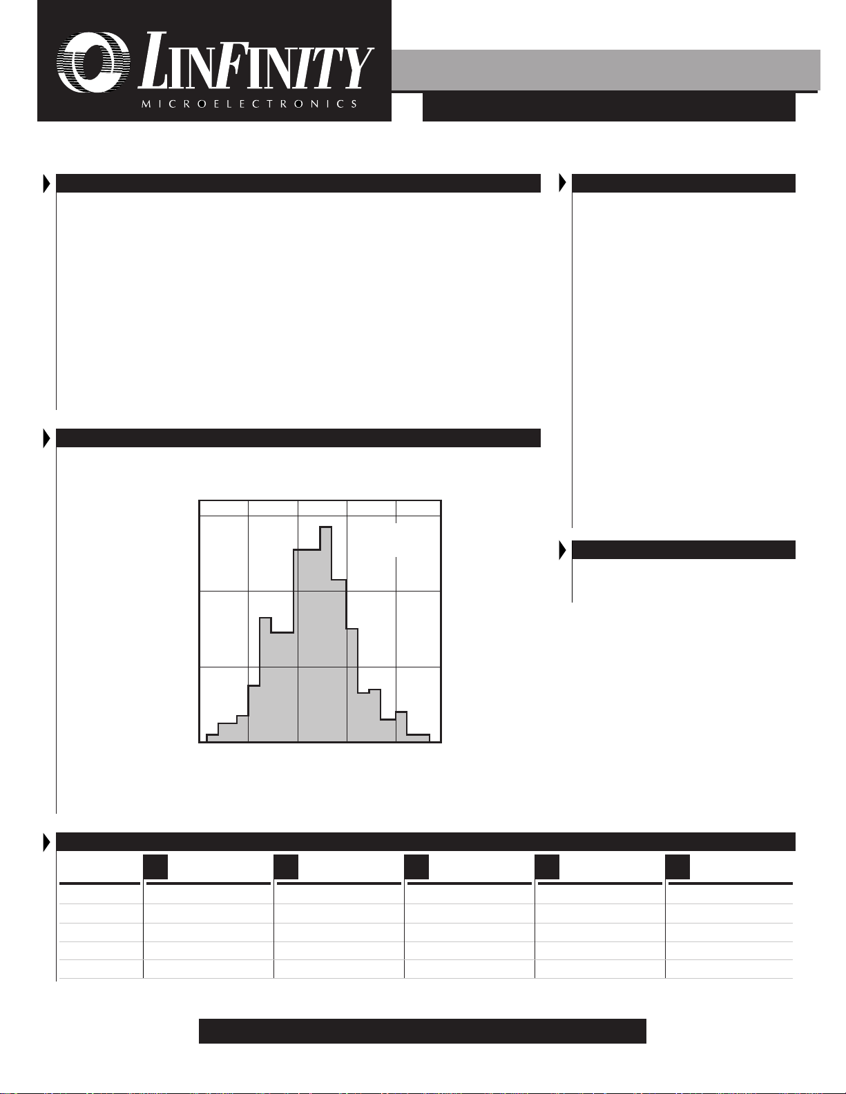
PRODUCT HIGHLIGHT
I NITIAL OSCILLATOR ACCURACY
15
10
Sample Size = 45
Sample Size = 279
Mean 411.887
Mean 401.661
Std. Dev. = 4.3
Std. Dev. = 3.8
N OT RECOMMENDED FOR NEW DESIGNS
KEY FEATURES
■■
■ IMPROVED REFERENCE INITIAL
■■
TOLERANCE (±1% max.)
■■
■ IMPROVED OSCILLATOR INITIAL
■■
ACCURACY (±3% typ.)
■■
■ IMPROVED STARTUP CURRENT
■■
(500µA typ.)
■■
■ PROP DELAY TO OUTPUTS (50ns typ.)
■■
p 10V TO 30V OPERATION
p 5.1V REFERENCE TRIMMED TO ±1%
p 2MHZ OSCILLATOR CAPABILITY
p 1.5A PEAK TOTEM-POLE DRIVERS
p U.V. LOCKOUT WITH HYSTERESIS
p NO OUTPUT DRIVER "FLOAT"
p PROGRAMMABLE SOFTSTART
p DOUBLE-PULSE SUPPRESSION LOGIC
p WIDEBAND LOW-IMPEDANCE ERROR
AMPLIFIER
p CURRENT-MODE OR VOLTAGE-MODE
CONTROL
p WIDE CHOICE OF HIGH-FREQUENCY
PACKAGES
HIGH RELIABILITY FEATURES
■■
■ AVAILABLE TO MIL-STD-883B
■■
■■
■ LINFINITY LEVEL "S" PROCESSING AVAIL.
■■
5
Percentage of Units - %
0
390 395 400 405 410
415
Initial Oscillator Accuracy - KHz
PACKAGE ORDER INFORMATION
T
(°C)
J
Plastic DIP
N
16-pin
0 to 70 SG3825CN SG3825CDW SG3825CQ SG3825CJ
-25 to 85 SG2825CN SG2825CDW SG2825CQ SG2825CJ
-55 to 125 SG1825CJ SG1825CL
MIL-STD-883 SG1825CJ/883B SG1825CL/883B
DESC SG1825CJ/DESC SG1825CL/DESC
Note: All surface-mount packages are available in Tape & Reel. Append the letter "T" to part number. (i.e. SG3825CDWT)
FOR FURTHER INFORMATION CALL (714) 898-8121
Copyright © 1994
Rev. 1.3 6/96
Plastic Wide SOIC
DW
16-pin
Plastic LCC
Q
20-pin
Ceramic DIP
J L
16-pin
11861 WESTERN AVENUE, GARDEN GROVE, CA. 92841
Ceramic LCC
20-pin
1

PRODUCT DATABOOK 1996/1997
SG1825C/SG2825C/SG3825C
H IGH-SPEED CURRENT-MODE PWM
OT RECOMMENDED FOR NEW DESIGNS
N
ABSOLUTE MAXIMUM RATINGS (Note 1)
Input Voltage (VIN and VC) .......................................................................................... 30V
Analog Inputs:
Error Amplifier and Ramp ........................................................................-0.3V to 7.0V
Softstart and I
Digital Input (Clock) .................................................................................... 1.5V to 6.0V
Driver Outputs ........................................................................................ -0.3V to V
Source / Sink Output Current (each output):
/S.D. ................................................................................ -0.3V to 6.0V
LIM
C
+1.5V
Continuous .............................................................................................................. 0.5A
Pulse, 500ns ............................................................................................................ 2.0A
Softstart Sink Current................................................................................................ 20mA
Clock Output Current ................................................................................................. 5mA
Error Amplifier Output Current ................................................................................. 5mA
Oscillator Charging Current ....................................................................................... 5mA
Operating Junction Temperature:
Hermetic (J, L Package) ....................................................................................... 150°C
Plastic (DW, N, Q Packages) ............................................................................... 150°C
Storage Temperature Range...................................................................... -65°C to 150°C
Lead Temperature (soldering, 10 seconds) ............................................................ 300°C
Note 1. Exceeding these ratings could cause damage to the device.
THERMAL DATA
N PACKAGE:
THERMAL RESISTANCE-JUNCTION TO AMBIENT,
DW PACKAGE:
THERMAL RESISTANCE-JUNCTION TO AMBIENT,
Q PACKAGE:
THERMAL RESISTANCE-JUNCTION TO AMBIENT,
J PACKAGE:
THERMAL RESISTANCE-JUNCTION TO AMBIENT,
L PACKAGE:
THERMAL RESISTANCE-JUNCTION TO CASE,
THERMAL RESISTANCE-JUNCTION TO AMBIENT,
Junction Temperature Calculation: TJ = TA + (P
The θ
numbers are guidelines for the thermal performance of the device/pc-board
JA
system. All of the above assume no ambient airflow.
θθ
θ
θθ
JA
θθ
θ
θθ
JA
θθ
θ
θθ
JA
θθ
θ
θθ
JA
θθ
θ
θθ
JC
θθ
θ
θθ
JA
x θ
).
D
JA
65°C/W
95°C/W
80°C/W
80°C/W
35°C/W
120°C/W
PACKAGE PIN OUTS
INV. INPUT
N.I. INPUT
E/A OUTPUT
CLOCK
SOFTSTART
INV. INPUT
N.I. INPUT
E/A OUTPUT
CLOCK
R
C
RAMP
SOFTSTART
418
616
814
1 16
215
314
413
512
R
T
611
C
T
710
RAMP
89
J & N PACKAGE
(Top View)
1 16
215
314
413
512
T
611
T
710
89
DW PACKAGE
(Top View)
321
4
5
6
7
8
911121310
Q PACKAGE
(Top View)
3212019
9 11121310
20 19
V
REF
+V
IN
OUTPUT B
V
C
PWR GND
OUTPUT A
GROUND
I
/ S.D.
LIM
+V
REF
+V
IN
OUTPUT B
V
C
PWR GND
OUTPUT A
GROUND
I
/ S.D.
LIM
18
17
16
15
14
175
157
L PACKAGE
(Top View)
1. N.C.
2. INV. INPUT
3. N.I. INPUT
4. E/A OUTPUT
5. CLOCK
6. N.C.
7. R
T
8. C
T
9. RAMP
10. SOFTSTART
2
11. N.C.
12. I
/ S.D.
LIM
13. GROUND
14. OUTPUT A
15. PWR GND
16. N.C.
17. V
C
18. OUTPUT B
19. +V
IN
20. V
REF
Copyright © 1994
Rev. 1.3 6/96

PRODUCT DATABOOK 1996/1997
H IGH-SPEED CURRENT-MODE PWM
N OT RECOMMENDED FOR NEW DESIGNS
RECOMMENDED OPERATING CONDITIONS (Note 2)
Parameter Symbol Units
Supply Voltage Range
Voltage Amp Common Mode Range
Ramp Input Voltage Range
Current Limit / Shutdown Voltage Range
Source / Sink Output Current
Continuous
Pulse, 500ns
Voltage Reference Output Current
Oscillator Frequency Range
Oscillator Charging Current
Oscillator Timing Resistor R
Oscillator Timing Capacitor C
Operating Ambient Temperature Range:
SG1825C T
SG2825C T
SG3825C T
Note 2. Range over which the device is functional.
SG1825C/SG2825C/SG3825C
Recommended Operating Conditions
Min. Typ. Max.
10 30 V
1.5 5.5 V
0 5.0 V
0 4.0 V
200 mA
1.0 A
110mA
4 1500 kHz
0.030 3 mA
T
T
A
A
A
1 100 kΩ
0.470 10 nF
070°C
-25 85 °C
-55 125 °C
ELECTRICAL CHARACTERISTICS (Note 3)
(Unless otherwise specified, these specifications apply over the operating ambient temperatures for SG3825C with 0°C ≤ TA ≤ 70°C, SG2825C with
-25°C ≤ TA ≤ 85°C, SG1825C with -55°C ≤ TA ≤ 125°C, and V
and case temperatures equal to the ambient temperature.)
Parameter
Symbol
=15V. Low duty cycle pulse testing techniques are used which maintains junction
IN=VC
Test Conditions
SG1825C/2825C
Min. Typ. Max. Min. Typ. Max.
SG3825C
Units
Reference Section
Output Voltage TJ = 25°C, IL = 1mA
Line Regulation VIN = 10 to 30V
Load Regulation IL = 1 to 10mA
Temperature Stability (Note 3) Over Operating Temperature
Total Output Range (Note 3) Over Line, Load, and Temperature
Output Noise Voltage (Note 3) f = 10Hz to 10kHz, IL = 0mA
Long Term Stability (Notes 3 &4) TJ = 125°C, t = 1000hrs
Short Circuit Current V
REF
= 0V
5.05 5.10 5.15 5.05 5.10 5.15 V
215 215 mV
515 515 mV
0.2 0.4 0.2 0.4 mV/°C
5.00 5.20 5.00 5.20 V
50 200 50 µV
525 525 mV
-15 -50 -100 -15 -50 -100 mA
RMS
Oscillator Section (Note 5)
Initial Accuracy TJ = 25°C, C
≤ 10pF
CLK
Voltage Stability VIN = 10 to 30V
Temperature Stability (Note 3) Over Rated Operating Temperature
Total Frequency Limits (Note 3) Over Line and Temperature
Minimum Frequency R
Maximum Frequency R
Clock High Level I
Clock Low Level I
= 100KΩ, C
T
= 1KΩ, C
T
= -1mA
CLK
= -1mA
CLK
= 0.01µF
T
= 470pF
T
Ramp Peak Voltage
Ramp Valley Voltage
Valley-to-Peak Amplitude
Note 3. This parameter is guaranteed by design and process control, but is not 100% tested in production.
Note 4. This parameter is non-accumulative, and represents the random fluctuation of the reference voltage within some error band when observed
over any 1000 hour period of time.
370 400 430 370 400 430 kHz
0.2 2 0.2 2 %
58 58 %
350 450 350 450 kHz
4 4 kHz
1.5 1.5 MHz
3.9 4.5 3.9 4.5 V
2.3 2.9 2.3 2.9 V
2.6 2.8 3.0 2.6 2.8 3.0 V
0.7 1.0 1.25 0.7 1.0 1.25 V
1.6 1.8 2.0 1.6 1.8 2.0 V
Copyright © 1994
Rev. 1.3 6/96
3
 Loading...