

Microchip Technology Inc PIC12CE673-04-JW, PIC12CE673-04-P, PIC12CE673-04E-JW, PIC12CE674-04-P, PIC12CE674-04E-JW Datasheet
...
M
PIC12CE67X
8-Pin, 8-Bit CMOS Microcontroller with A/D Converter
and EEPROM Data Memory
Devices:
PIC12CE673 and PIC12CE674 are 8-bit OTP microcontrollers with 8-bit A/D Converter and EEPROM data
memory packaged in 8-lead packages. They are based
on the 14-bit PICmicro™ MCU architecture.
High-Performance RISC CPU:
• Only 35 single word instructions to learn
• All instructions are single cycle (400 ns) except for
program branches which are two-cycle
• Operating speed: DC - 10 MHz clock input
Device
PIC12CE673 1024 x 14 128 x 8 16 x 8
PIC12CE674 2048 x 14 128 x 8 16 x 8
• 14-bit wide instructions
• 8-bit wide data path
• Interrupt capability
• Special function hardware registers
• 8-level deep hardware stack
• Direct, indirect and relative addressing modes for
data and instructions
DC - 400 ns instruction cycle
Memory
Program
Data
RAM
Data
EEPROM
Peripheral Features:
• 8-bit real time clock/counter (TMR0) with 8-bit
programmable prescaler
• Interrupt on pin change (GP0, GP1, GP3)
• 1,000,000 erase/write cycle EEPROM data
memory
• EEPROM data retention > 40 years
• Four-channel, 8-bit A/D converter
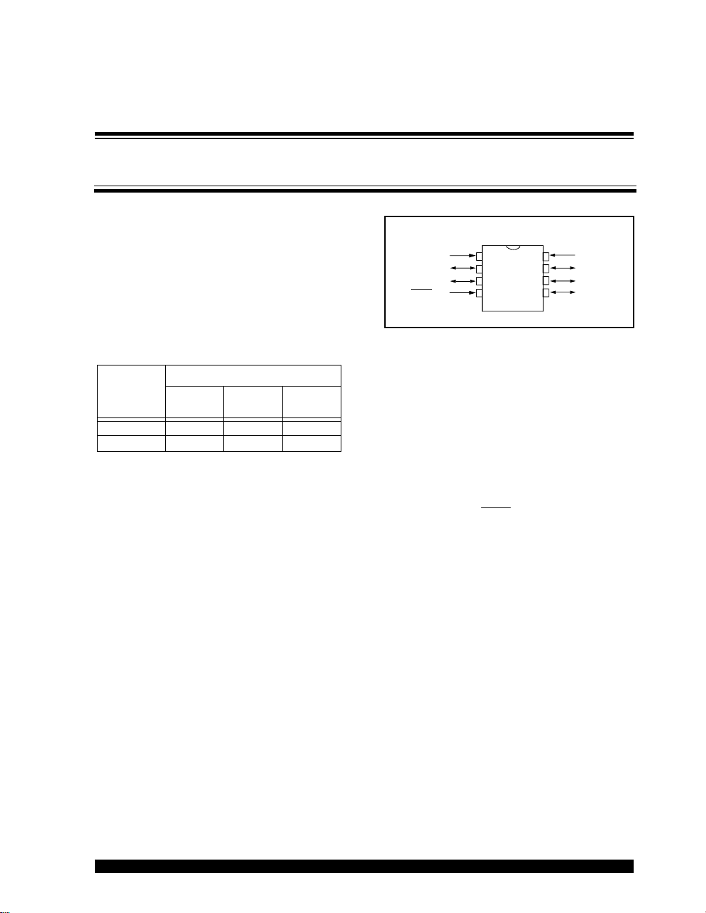
Pin Diagram:
PDIP , Windo wed CERDIP
PIC12CE673
CLKOUT
GP3/MCLR
VDD
/VPP
GP5/OSC1/CLKIN
GP4/OSC2/AN3/
PIC12CE674
1
2
3
4
VSS
8
GP0/AN0
7
GP1/AN1/V
6
5
GP2/T0CKI/
AN2/INT
Special Microcontroller Features:
• In-Circuit Serial Programming (ICSP™)
• Internal 4 MHz oscillator with programmable
calibration
• Selectable clockout
• Power-on Reset (POR)
• Power-up Timer (PWRT) and Oscillator Start-up
Timer (OST)
• Watchdog Timer (WDT) with its own on-chip RC
oscillator for reliable operation
• Programmable code protection
• Power saving SLEEP mode
• Internal pull-ups on I/O pins (GP0, GP1)
• Internal pull-up on MCLR
• Selectable oscillator options:
- INTRC: Precision internal 4 MHz oscillator
- EXTRC: External low-cost RC oscillator
- XT: Standard crystal/resonator
- HS: High speed crystal/resonator
- LP: Power saving, low frequency crystal
pin
CMOS Technology:
• Low-power, high-speed CMOS EPROM/
EEPROM technology
• Fully static design
• Wide operating voltage range 2.5V to 5.5V
• Commercial, Industrial, and Extended
temperature ranges
• Low power consumption
< 2 mA @ 5V, 4 MHz
15 µA typical @ 3V, 32 kHz
< 1 µA typical standby current
REF
1998 Microchip Technology Inc.
Preliminary
DS40181A-page 1

PIC12CE67X
Table of Contents
1.0 General Description....................................................................................................................................................................... 3
2.0 PIC12CE67X Device Varieties....................................................................................................................................................... 5
3.0 Architectural Overview...................................................................................................................................................................7
4.0 Memory Organization................................................................................................................................................................... 11
5.0 I/O Port......................................................................................................................................................................................... 25
6.0 EEPROM Peripheral Operation................................................................................................................................................... 27
7.0 Timer0 Module.............................................................................................................................................................................31
8.0 Analog-to-Digital Converter (A/D) Module ................................................................................................................................... 37
9.0 Special Features of the CPU ....................................................................................................................................................... 45
10.0 Instruction Set Summary..............................................................................................................................................................61
11.0 Development Support .................................................................................................................................................................. 75
12.0 Electrical Characteristics for PIC12CE67X .................................................................................................................................. 79
13.0 DC and AC Characteristics - PIC12CE67X ................................................................................................................................. 95
14.0 Packaging Information ............................................................................................................................................................... 101
Appendix A: Code for Accessing EEPROM Data Memory ............................................................................................................ 105
Index .................................................................................................................................................................................................. 107
On-Line Support................................................................................................................................................................................. 111
PIC12CE67X Product Identification System ..................................................................................................................................... 113
To Our Valued Customers
We constantly strive to improve the quality of all our products and documentation. We have spent an exceptional
amount of time to ensure that these documents are correct. However, we realize that we may have missed a few
things. If you find any information that is missing or appears in error, please use the reader response form in the
back of this data sheet to inform us. We appreciate your assistance in making this a better document.
DS40181A-page 2
Preliminary
1998 Microchip Technology Inc.

PIC12CE67X
1.0 GENERAL DESCRIPTION
The PIC12CE67X devices are low-cost, high-performance, CMOS, fully-static, 8-bit microcontroller with
integrated analog-to-digital (A/D) converter and
EEPROM data memory in the PIC12CEXXX Microcontroller family.
All PICmicro™ microcontrollers employ an advanced
RISC architecture. The PIC12CE67X microcontrollers
have enhanced core features, eight-level deep stack,
and multiple internal and external interrupt sources.
The separate instruction and data buses of the Harvard
architecture allow a 14-bit wide instruction word with
the separate 8-bit wide data. The two stage instruction
pipeline allows all instructions to execute in a single
cycle, except for program branches which require two
cycles. A total of 35 instructions (reduced instruction
set) are available. Additionally, a large register set gives
some of the architectural innovations used to achiev e a
very high performance.
PIC12CE67X microcontrollers typically achieve a 2:1
code compression and a 4:1 speed improvement over
other 8-bit microcontrollers in their class.
The PIC12CE67X devices ha ve 128 b ytes of RAM, 16
bytes of EEPROM data memory, 5 I/O
pin. In addition a timer/counter is available. Also a 4channel high-speed 8-bit A/D is provided. The 8-bit resolution is ideally suited for applications requiring lowcost analog interface, e.g. thermostat control, pressure
sensing, etc.
The PIC12CE67X device has special features to
reduce external components, thus reducing cost,
enhancing system reliability and reducing power consumption. The PIC12CE67X products are equipped
with special features that reduce system cost and
power requirements. The Power-On Reset (POR),
Power-up Timer (PWRT), and Oscillator Start-up Timer
(OST) eliminate the need for external reset circuitry.
There are five oscillator configurations to choose from,
including INTRC precision internal oscillator mode and
the power-saving LP (Low Power) oscillator. Power
saving SLEEP mode, Watchdog Timer and code
protection features improve system cost, power and
reliability.The SLEEP (power-down) feature provides a
power saving mode. The user can wake up the chip
from SLEEP through several external and internal
interrupts and resets.
pins and 1 input
A highly reliable Watchdog Timer with its own on-chip
RC oscillator provides protection against software lockup.
A UV erasable windowed package version is ideal for
code development while the cost-effective One-TimeProgrammable (OTP) version is suitable for production
in any volume. The customer can take full advantage of
Microchip’s price leadership in OTP microcontrollers
while benefiting from the OTP’s flexibility.
The PIC12CE67X device fits perfectly in applications
ranging from security and remote sensors to appliance
control and automotive. The EPROM technology
makes customization of application programs (transmitter codes, motor speeds, receiver frequencies, etc.)
extremely fast and convenient. The small footprint
packages make this microcontroller series perfect for
all applications with space limitations. Low cost, low
power, high perf ormance, ease of use and I/O flexibility
make the PIC12CE67X very versatile even in areas
where no microcontroller use has been considered
before (e.g. timer functions, communications and
coprocessor applications).
1.1 F
The PIC12CE67X products are compatible with other
members of the 14-Bit, PIC12C67X and PIC16CXXX
families.
1.2 De
The PIC12CE67X device is supported by a full-featured macro assembler, a software simulator, an in-circuit emulator, a low-cost de velopment prog rammer and
a full-featured programmer. A “C” compiler and fuzzy
logic support tools are also available.
amily and Upward Compatibility
velopment Support
1998 Microchip Technology Inc.
Preliminary
DS40181A-page 3

PIC12CE67X
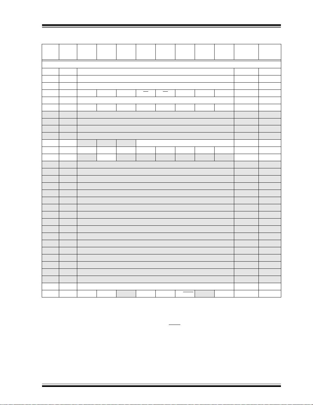
TABLE 1-1: PIC12CXXX & PIC12CEXXX FAMILY OF DEVICES
Clock
Memory
Peripherals
Features
PIC12C508(A)
Maximum
Frequency
of Operation
(MHz)
EPROM
Program
Memory
RAM Data
Memory
(bytes)
EEPROM
Data Memory
(bytes)
Timer
Module(s)
A/D Converter (8-bit)
Channels
Wake-up
from SLEEP
on pin
change
Interrupt
Sources
I/O Pins 5 5 5 5 5 5 5 5
Input Pins 1 1 1 1 1 1 1 1
Internal
Pull-ups
In-Circuit
Serial
Programming
Number of
Instructions
Packages 8-pin DIP,
4 4 4 4 10 10 10 10
512 x 12 1024 x 12 512 x 12 1024 x 12 1024 x 14 2048 x 14 1024 x 14 2048 x 14
25 41 25 41 128 128
— — 16 16 — —
TMR0 TMR0 TMR0 TMR0 TMR0 TMR0 TMR0 TMR0
— — — — 4 4 4 4
Yes Yes Yes Yes Yes Yes Yes Yes
— — 4 4 4 4
Yes Yes Yes Yes Yes Yes Yes Yes
Yes Yes Yes Yes Yes Yes Yes Yes
33 33 33 33 35 35 35 35
JW, SOIC
PIC12C509(A) PIC12CE518 PIC12CE519 PIC12C671 PIC12C672 PIC12CE673 PIC12CE674
8-pin DIP,
JW, SOIC
8-pin DIP,
JW, SOIC
8-pin DIP,
JW, SOIC
8-pin DIP,
JW, SOIC
8-pin DIP,
JW, SOIC
128 128
16 16
8-pin DIP, JW8-pin DIP,
JW
All PIC12CXXX & PIC12CEXXX devices have Power-on Reset, selectable Watchdog Timer, selectable
code protect and high I/O current capability.
All PIC12CXXX & PIC12CEXXX devices use serial programming with data pin GP0 and clock pin GP1.
DS40181A-page 4
Preliminary
1998 Microchip Technology Inc.

PIC12CE67X
2.0 PIC12CE67X DEVICE
VARIETIES
A variety of frequency ranges and packaging options
are available. Depending on application and production
requirements, the proper device option can be selected
using the information in the PIC12CE67X Product
Identification System section at the end of this data
sheet. When placing orders, please use that page of
the data sheet to specify the correct part number.
For the PIC12CE67X, the device “type” is indicated in
the device number:
1.CE, as in PIC12CE671. These devices have
OTP program memory, EEPROM data memory
and operate over the standard voltage range.
2.1 UV Erasab
The UV erasable version, offered in windowed package, is optimal for prototype dev elopment and pilot programs.
The UV erasable version can be erased and reprogrammed to any of the configuration modes.
Microchip's PICSTART Plus and PRO MATE programmers both support the PIC12CE67X. Third party
programmers also are available; refer to the Microchip
Third Party Guide for a list of sources.
Note:
Please note that erasing the device will
also erase the pre-programmed internal
calibration value for the internal oscillator.
The calibration value must be saved prior
to erasing the part.
2.2 One-Time-Pr
Devices
The availability of OTP devices is especially useful for
customers who need the flexibility for frequent code
updates and small volume applications.
The OTP devices, packaged in plastic packages, permit the user to program them once. In addition to the
program memory, the configuration bits must also be
programmed.
le Devices
ogrammable (OTP)
2.3 Quic
k-Turn-Programming (QTP)
Devices
Microchip offers a QTP Programming Service for factory production orders. This service is made available
for users who choose not to program a medium to high
quantity of units and whose code patterns have stabilized. The devices are identical to the OTP devices but
with all EPROM locations and configuration options
already programmed by the factory. Certain code and
prototype verification procedures apply before production shipments are available. Please contact your local
Microchip Technology sales office for more details.
2.4 Serializ
Microchip offers a unique programming service where
a few user-defined locations in each device are programmed with different serial numbers. The serial numbers may be random, pseudo-random, or sequential.
Serial programming allows each device to have a
unique number which can serve as an entry-code,
password, or ID number.
ed Quick-Turn Programming
SM
(SQTP
Devices
)
1998 Microchip Technology Inc.
Preliminary
DS40181A-page 5

PIC12CE67X
NOTES:
DS40181A-page 6
Preliminary
1998 Microchip Technology Inc.

PIC12CE67X
3.0 ARCHITECTURAL OVERVIEW
The high performance of the PIC12CE67X family can
be attributed to a number of architectural features commonly found in RISC microprocessors. To begin with,
the PIC12CE67X uses a Harvard architecture, in which
program and data are accessed from separate memories using separate buses. This improves bandwidth
over traditional von Neumann architecture in which program and data are fetched from the same memory
using the same bus. Separating program and data
buses also allow instructions to be sized differently than
the 8-bit wide data word. Instruction opcodes are 14bits wide making it possible to have all single word
instructions. A 14-bit wide program memory access
bus fetches a 14-bit instruction in a single cycle. A twostage pipeline overlaps fetch and execution of instructions (Example 3-1). Consequently, all instructions (35)
execute in a single cycle (1 µs @ 4 MHz) except for program branches.
The table below lists program memory (EPROM), data
memory (RAM), and non-volatile memory (EEPROM)
for each PIC12CE67X device.
Device
PIC12CE673 1K x 14 128 x 8 16x8
PIC12CE674 2K x 14 128 x 8 16x8
Program
Memory
RAM
Data
Memory
EEPROM
Data
Memory
The PIC12CE67X can directly or indirectly address its
register files or data memory. All special function registers, including the program counter, are mapped in the
data memory. The PIC12CE67X has an orthogonal
(symmetrical) instruction set that makes it possible to
carry out any operation on any register using any
addressing mode. This symmetrical nature and lack of
‘special optimal situations’ mak e prog r amming with the
PIC12CE67X simple yet efficient. In addition, the learning curve is reduced significantly.
PIC12CE67X devices contain an 8-bit ALU and working register. The ALU is a general purpose arithmetic
unit. It performs arithmetic and Boolean functions
between the data in the working register and any register file.
The ALU is 8-bits wide and capable of addition, subtraction, shift and logical operations. Unless otherwise
mentioned, arithmetic operations are two's complement in nature. In two-operand instructions, typically
one operand is the working register (W register). The
other operand is a file register or an immediate constant. In single operand instructions, the operand is
either the W register or a file register.
The W register is an 8-bit working register used for ALU
operations. It is not an addressable register.
Depending on the instruction executed, the ALU may
affect the values of the Carry (C), Digit Carry (DC), and
Zero (Z) bits in the ST ATUS register. The C and DC bits
operate as a borro
respectively, in subtraction. See the
instructions for examples.
w bit and a digit borrow out bit,
SUBLW
and
SUBWF
1998 Microchip Technology Inc.
Preliminary
DS40181A-page 7
PIC12CE67X
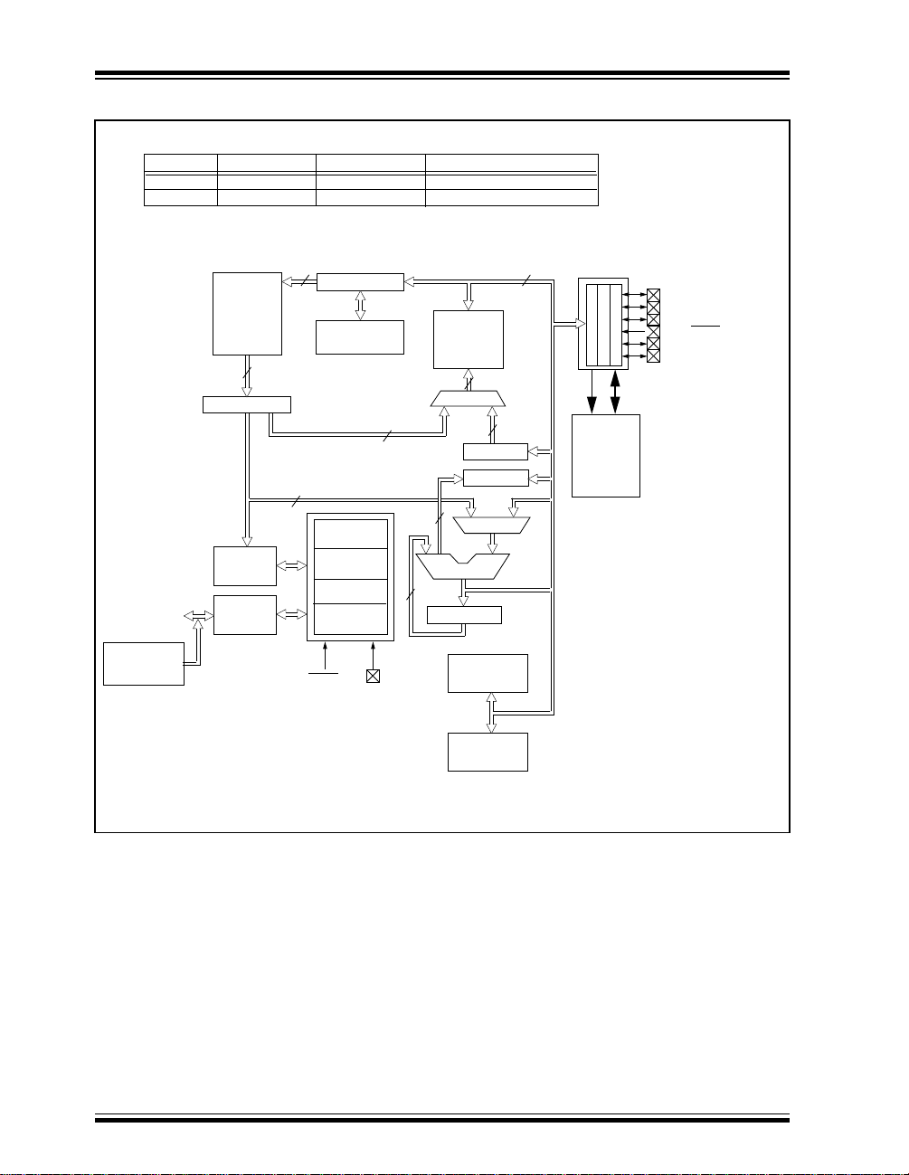
FIGURE 3-1: PIC12CE67X BLOCK DIAGRAM
PIC12CE673
PIC12CE674
OSC1/CLKIN
OSC2/CLKOUT
Internal
4 MHz Clock
Device
Program
Bus
Program Memory Data Memory (RAM)
1K x 14
2K x 14
EPROM
Program
Memory
14
Instruction reg
Instruction
Decode &
Control
Timing
Generation
8
13
Program Counter
8 Level Stack
Direct Addr
Power-up
Timer
Oscillator
Start-up Timer
Watchdog
Timer
Power-on
Reset
MCLR
128 x 8
128 x 8
(13 bit)
VDD, VSS
Non-Volatile Memory (EEPROM)
Data Bus
RAM
128 bytes
File
Registers
(1)
RAM Addr
7
8
3
9
Addr MUX
8
FSR reg
STATUS reg
MUX
ALU
W reg
Timer0
16 x 8
16 x 8
Indirect
Addr
8
GPIO
SCL
16x8
EEPROM
Data
Memory
GP0/AN0
GP1/AN1/VREF
GP2/T0CKI/AN2/INT
GP3/MCLR/Vpp
GP4/OSC2/AN3/CLKOUT
GP5/OSC1/CLKIN
SDA
Note 1: Higher order bits are from the STATUS register.
DS40181A-page 8
Preliminary
A/D
1998 Microchip Technology Inc.

PIC12CE67X
TABLE 3-1: PIC12CE67X PINOUT DESCRIPTION
DIP
Name
GP0/AN0 7 7 I/O TTL/ST Bi-directional I/O port/serial programming data/analog
GP1/AN1/V
GP2/T0CKI/AN2/INT 5 5 I/O ST Bi-directional I/O port/analog input 2. Can be config-
GP3/MCLR
GP4/OSC2/AN3/
CLKOUT
GP5/OSC1/CLKIN 2 2 I/O TTL/ST Bidirectional IO port oscillator crystal input/external
V
DD
SS
V
REF
/V
PP
Legend: I = input, O = output, I/O = input/output, P = power, — = not used, TTL = TTL input,
ST = Schmitt Trigger input
Pin #
SOIC
Pin #
6 6 I/O TTL/ST Bi-directional I/O port/serial programming clock/analog
4 4 I TTL Input port/master clear (reset) input/programming volt-
3 3 I/O TTL Bi-directional I/O port/oscillator crystal output/analog
1 1 P — Positive supply for logic and I/O pins
8 8 P — Ground reference for logic and I/O pins
I/O/P
Type
Buffer
Type
Description
input 0. Can be software programmed for internal
weak pull-up and interrupt on pin change. This b uffer is
a Schmitt Trigger input when used in serial programming mode.
input 1/voltage reference. Can be software programmed for internal weak pull-up and interrupt on pin
change. This buffer is a Schmitt Trigger input when
used in serial programming mode.
ured as T0CKI or external interrupt.
age input. When configured as MCLR
active low reset to the device. Voltage on MCLR
must not exceed VDD during normal device operation.
Can be software programmed for internal weak pull-up
and interrupt on pin change. W eak pull-up alw ays on if
configured as MCLR
input 3. Connections to crystal or resonator in crystal
oscillator mode (XT and LP modes only , GPIO in other
modes). In EXTRC and INTRC modes, the pin output
can be configured to CLKOUT which has 1/4 the frequency of OSC1 and denotes the instruction cycle
rate.
clock source input (GPIO in INTRC mode only, OSC1
in all other oscillator modes). Schmitt trigger in EXTRC
mode only.
.
, this pin is an
/V
PP
1998 Microchip Technology Inc.
Preliminary
DS40181A-page 9
PIC12CE67X
3.1 Cloc
king Scheme/Instruction Cycle
The clock input (from OSC1) is internally divided by
four to generate four non-overlapping quadrature
clocks namely Q1, Q2, Q3 and Q4. Internally, the program counter (PC) is incremented every Q1, the
instruction is fetched from the program memory and
latched into the instruction register in Q4. The instruction is decoded and executed during the following Q1
through Q4. The clocks and instruction execution flow
is shown in Figure 3-2.
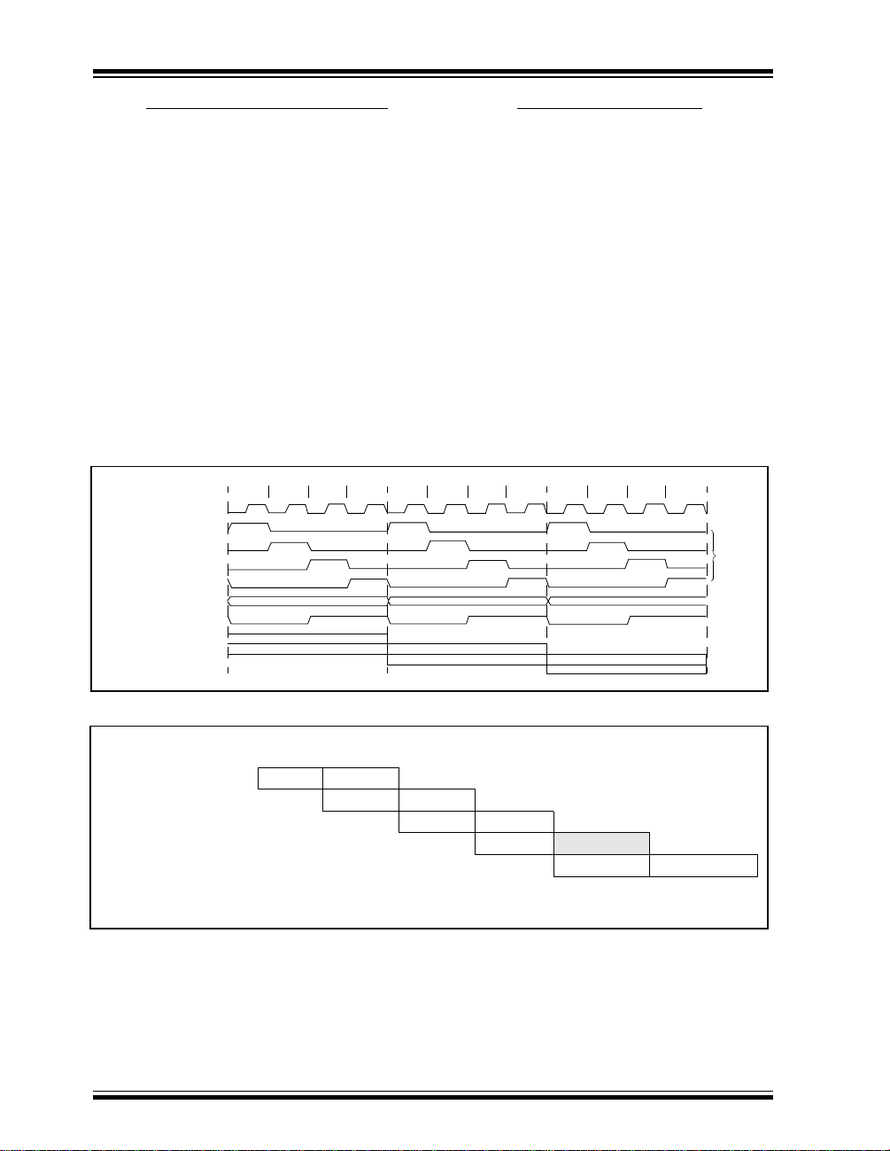
FIGURE 3-2: CLOCK/INSTRUCTION CYCLE
Q2 Q3 Q4
Q1
OSC1
Q1
Q2
Q3
Q4
PC
OSC2/CLKOUT
(EXTRC and
INTRC modes)
PC PC+1 PC+2
Fetch INST (PC)
Execute INST (PC-1) Fetch INST (PC+1)
3.2 Instruction Flo
An “Instruction Cycle” consists of four Q cycles (Q1,
Q2, Q3 and Q4). The instruction fetch and execute
are pipelined such that fetch takes one instruction
cycle while decode and execute takes another
instruction cycle. However, due to the pipelining,
each instruction effectively executes in one cycle. If
an instruction causes the program counter to change
(e.g.
GOTO
the instruction (Example 3-1).
A fetch cycle begins with the program counter (PC)
incrementing in Q1.
In the execution cycle, the fetched instruction is
latched into the “Instruction Register" (IR) in cycle
Q1. This instruction is then decoded and executed
during the Q2, Q3, and Q4 cycles. Data memory is
read during Q2 (operand read) and written during Q4
(destination write).
Q2 Q3 Q4
Q1
Execute INST (PC) Fetch INST (PC+2)
) then two cycles are required to complete
Q1
Execute INST (PC+1)
w/Pipelining
Q2 Q3 Q4
Internal
phase
clock
EXAMPLE 3-1: INSTRUCTION PIPELINE FLOW
Tcy0 Tcy1 Tcy2 Tcy3 Tcy4 Tcy5
1. MOVLW 55h
2. MOVWF GPIO
3. CALL SUB_1
4. BSF GPIO, BIT3 (Forced NOP)
5. Instruction @ address SUB_1
All instructions are single cycle, except for any progr am branches . These take two cycles since the fetch instruction is “flushed” from the pipeline while the new instruction is being fetched and then executed.
DS40181A-page 10
Fetch 1 Execute 1
Fetch 2 Execute 2
Fetch 3 Execute 3
Preliminary
Fetch 4 Flush
Fetch SUB_1 Execute SUB_1
1998 Microchip Technology Inc.

PIC12CE67X
4.0 MEMORY ORGANIZATION
4.1 Pr
The PIC12CE67X has a 13-bit program counter capable of addressing an 8K x 14 program memory space.
For the PIC12CE673 the first 1K x 14 (0000h-03FFh) is
implemented.
For the PIC12CE674, the first 2K x 14 (0000h-07FFh)
is implemented. Accessing a location above the physically implemented address will cause a wraparound.
The reset vector is at 0000h and the interrupt vector is
at 0004h.
FIGURE 4-1: PIC12CE67X PROGRAM
ogram Memory Organization
MEMORY MAP AND STACK
PC<12:0>
CALL, RETURN
RETFIE, RETLW
Stack Level 1
Stack Level 8
Reset Vector
Peripheral
Interrupt Vector
13
0000h
0004h
0005h
4.2 Data Memor
The data memory is partitioned into two Banks which
contain the General Purpose Registers and the Special
Function Registers. Bit RP0 is the bank select bit.
RP0 (STATUS<5>) = 1 → Bank 1
RP0 (STATUS<5>) = 0 → Bank 0
Each Bank extends up to 7Fh (128 bytes). The lower
locations of each Bank are reserved for the Special
Function Registers. Abo v e the Special Function Registers are General Purpose Registers implemented as
static RAM. Both Bank 0 and Bank 1 contain special
function registers. Some "high use" special function
registers from Bank 0 are mirrored in Bank 1 for code
reduction and quicker access.
Also note that F0h through FFh on the PIC12CE67X is
mapped into Bank 0 registers 70h-7Fh.
4.2.1 GENERAL PURPOSE REGISTER FILE The register file can be accessed either directly , or indi-
rectly through the File Select Register FSR
(Section 4.5).
y Organization
On-chip Program
Memory
(PIC12CE674 only)
1998 Microchip Technology Inc.
03FFh
0400h
07FFh
0800h
1FFFh
Preliminary
DS40181A-page 11
PIC12CE67X
FIGURE 4-2: PIC12CE67X REGISTER FILE
MAP
File
Address
00h
01h
02h
03h
04h
05h
06h
07h
08h
09h
0Ah
0Bh
0Ch
0Dh
0Eh
0Fh
10h
11h
12h
13h
14h
15h
16h
17h
18h
19h
1Ah
1Bh
1Ch
1Dh
1Eh
1Fh
20h
70h
7Fh
(1)
INDF
TMR0
PCL
STATUS
FSR
GPIO
PCLATH
INTCON
PIR1
ADRES
ADCON0
General
Purpose
Register
Bank 0 Bank 1
INDF
OPTION
PCL
STATUS
FSR
TRIS
PCLATH
INTCON
PIE1
PCON
OSCCAL
ADCON1
General
Purpose
Register
Mapped
in Bank 0
File
Address
(1)
80h
81h
82h
83h
84h
85h
86h
87h
88h
89h
8Ah
8Bh
8Ch
8Dh
8Eh
8Fh
90h
91h
92h
93h
94h
95h
96h
97h
98h
99h
9Ah
9Bh
9Ch
9Dh
9Eh
9Fh
A0h
BFh
C0h
EFh
F0h
FFh
4.2.2 SPECIAL FUNCTION REGISTERS The Special Function Registers are registers used by
the CPU and Peripheral Modules for controlling the
desired operation of the device. These registers are
implemented as static RAM.
The special function registers can be classified into two
sets (core and peripheral). Those registers associated
with the “core” functions are described in this section,
and those related to the operation of the peripheral
features are described in the section of that peripheral
feature.
Unimplemented data memory locations, read
as '0'.
Note 1: Not a physical register.
DS40181A-page 12
Preliminary
1998 Microchip Technology Inc.
PIC12CE67X
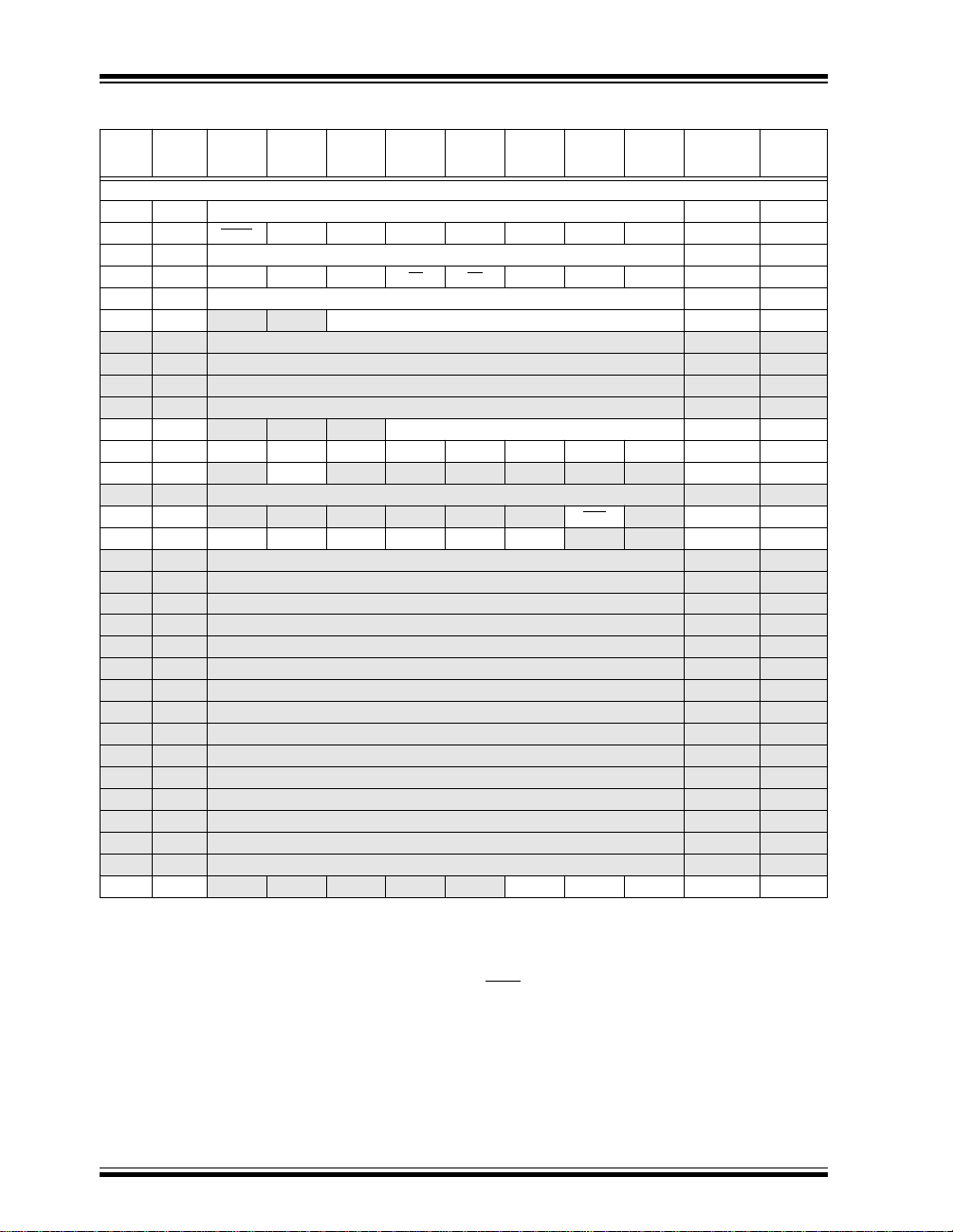
TABLE 4-1: PIC12CE67X SPECIAL FUNCTION REGISTER SUMMARY
Address Name Bit 7 Bit 6 Bit 5 Bit 4 Bit 3 Bit 2 Bit 1 Bit 0
Bank 0
(1)
00h
INDF Addressing this location uses contents of FSR to address data memory (not a physical register)
01h TMR0 Timer0 module’s register
(1)
02h
PCL Program Counter's (PC) Least Significant Byte
(1)
03h
STATUS IRP
(1)
FSR Indirect data memory address pointer
04h
05h GPIO SCL SDA GP5 GP4 GP3 GP2 GP1 GP0
06h
07h — Unimplemented — —
08h — Unimplemented — —
09h — Unimplemented — —
0Ah
0Bh
0Ch PIR1 — ADIF — — — — — — -0-- ---- -0-- ----
0Dh — Unimplemented — —
0Eh — Unimplemented — —
0Fh — Unimplemented — —
10h — Unimplemented — —
11h — Unimplemented — —
12h — Unimplemented — —
13h — Unimplemented — —
14h — Unimplemented — —
15h — Unimplemented — —
16h — Unimplemented — —
17h — Unimplemented — —
18h — Unimplemented — —
19h — Unimplemented — —
1Ah — Unimplemented — —
1Bh — Unimplemented — —
1Ch — Unimplemented — —
1Dh — Unimplemented — —
1Eh ADRES A/D Result Register xxxx xxxx uuuu uuuu
1Fh ADCON0 ADCS1 ADCS0 r CHS1 CHS0 GO/DONE r ADON 0000 0000 0000 0000
— Unimplemented — —
(1,2)
PCLATH
(1)
INTCON GIE PEIE T0IE INTE GPIE T0IF INTF GPIF 0000 000x 0000 000u
(4)
— — — Write Buffer for the upper 5 bits of the Program Counter
RP1
(4)
RP0 T
O PD Z DC C
Value on
Power-on
Reset
0000 0000 0000 0000
xxxx xxxx uuuu uuuu
0000 0000 0000 0000
0001 1xxx 000q quuu
xxxx xxxx uuuu uuuu
11xx xxxx 11uu uuuu
---0 0000 ---0 0000
Legend: x = unknown, u = unchanged, q = value depends on condition, - = unimplemented read as '0', r = reserved.
Shaded locations are unimplemented, read as ‘0’.
Note 1: These registers can be addressed from either bank.
2: The upper byte of the program counter is not directly accessible. PCLATH is a holding register for the PC<12:8> whose
contents are transferred to the upper byte of the program counter.
3: Other (non power-up) resets include external reset through MCLR and Watchdog Timer Reset.
4: The IRP and RP1 bits are reserved on the PIC12CE67X, always maintain these bits clear.
Value on
all other
Resets
(3)
1998 Microchip Technology Inc.
Preliminary
DS40181A-page 13
PIC12CE67X
TABLE 4-1: PIC12CE67X SPECIAL FUNCTION REGISTER SUMMARY (CONT.)
Address Name Bit 7 Bit 6 Bit 5 Bit 4 Bit 3 Bit 2 Bit 1 Bit 0
Bank 1
(1)
80h
INDF Addressing this location uses contents of FSR to address data memory (not a physical register) 0000 0000 0000 0000
81h OPTION GPPU INTEDG T0CS T0SE PSA PS2 PS1 PS0 1111 1111 1111 1111
(1)
82h
PCL Program Counter's (PC) Least Significant Byte 0000 0000 0000 0000
(1)
83h
STATUS IRP
(1)
84h
FSR Indirect data memory address pointer xxxx xxxx uuuu uuuu
85h TRIS — — GPIO Data Direction Register 0011 1111 0011 1111
86h — Unimplemented — —
87h — Unimplemented — —
88h — Unimplemented — —
89h — Unimplemented — —
(1,2)
8Ah
PCLATH — — — Write Buffer for the upper 5 bits of the PC ---0 0000 ---0 0000
(1)
8Bh
INTCON GIE PEIE T0IE INTE GPIE T0IF INTF GPIF 0000 000x 0000 000x
8Ch PIE1 — ADIE — — — — — — -0-- ---- -0-- ----
8Dh — Unimplemented — —
8Eh PCON — — — — — — POR — ---- --0- ---- --u-
8Fh OSCCAL CAL5 CAL4 CAL3 CAL2 CAL1 CAL0 — — 1000 00-- uuuu uu--
90h — Unimplemented — —
91h — Unimplemented — —
92h — Unimplemented — —
93h — Unimplemented — —
94h — Unimplemented — —
95h — Unimplemented — —
96h — Unimplemented — —
97h — Unimplemented — —
98h — Unimplemented — —
99h — Unimplemented — —
9Ah — Unimplemented — —
9Bh — Unimplemented — —
9Ch — Unimplemented — —
9Dh — Unimplemented — —
9Eh — Unimplemented — —
9Fh ADCON1 — — — — — PCFG2 PCFG1 PCFG0 ---- -000 ---- -000
(4)
RP1
(4)
RP0 TO PD Z DC C 0001 1xxx 000q quuu
Value on
Power-on
Reset
Legend: x = unknown, u = unchanged, q = value depends on condition, - = unimplemented read as '0', r = reserved.
Shaded locations are unimplemented, read as ‘0’.
Note 1: These registers can be addressed from either bank.
2: The upper byte of the program counter is not directly accessible. PCLATH is a holding register for the PC<12:8> whose
contents are transferred to the upper byte of the program counter.
3: Other (non power-up) resets include external reset through MCLR and Watchdog Timer Reset.
4: The IRP and RP1 bits are reserved on the PIC12CE67X, always maintain these bits clear.
Value on
all other
Resets
(3)
DS40181A-page 14 Preliminary 1998 Microchip Technology Inc.

PIC12CE67X
4.2.2.1 STATUS REGISTER
The STATUS register, shown in Figure 4-3, contains
the arithmetic status of the ALU, the RESET status and
the bank select bits for data memory.
The STATUS register can be the destination for any
instruction, as with any other register. If the STATUS
register is the destination for an instruction that affects
the Z, DC or C bits, then the write to these three bits is
disabled. These bits are set or cleared according to the
device logic. Further more, the T
writable. Therefore, the result of an instruction with the
STATUS register as destination may be different than
intended.
For example, CLRF STATUS will clear the upper-three
bits and set the Z bit. This lea v es the STATUS register
as 000u u1uu (where u = unchanged).
O and PD bits are not
It is recommended, therefore, that only BCF, BSF,
SWAPF and MOVWF instructions are used to alter the
STATUS register because these instructions do not
affect the Z, C or DC bits from the STATUS register. For
other instructions, not affecting any status bits, see the
"Instruction Set Summary."
Note 1: Bits IRP and RP1 (STATUS<7:6>) are not
used by the PIC12CE67X and should be
maintained clear. Use of these bits as
general purpose R/W bits is NOT recommended, since this may affect upward
compatibility with future products.
Note 2: The C and DC bits operate as a borro
and digit borrow bit, respectively, in subtraction. See the SUBLW and SUBWF
instructions for examples.
FIGURE 4-3: STATUS REGISTER (ADDRESS 03h, 83h)
Reserved Reserved R/W-0 R-1 R-1 R/W-x R/W-x R/W-x
IRP RP1 RP0 TO PD Z DC C R = Readable bit
bit7 bit0
bit 7: IRP: Register Bank Select bit (used for indirect addressing)
1 = Bank 2, 3 (100h - 1FFh)
0 = Bank 0, 1 (00h - FFh)
The IRP bit is reserved, always maintain this bit clear.
bit 6-5: RP1:RP0: Register Bank Select bits (used for direct addressing)
11 = Bank 3 (180h - 1FFh)
10 = Bank 2 (100h - 17Fh)
01 = Bank 1 (80h - FFh)
00 = Bank 0 (00h - 7Fh)
Each bank is 128 bytes. The RP1 bit is reserved, always maintain this bit clear.
bit 4: T
bit 3: PD
bit 2: Z: Zero bit
bit 1: DC: Digit carry/borro
bit 0: C: Carry/borro
O: Time-out bit
1 = After power-up, CLRWDT instruction, or SLEEP instruction
0 = A WDT time-out occurred
: Power-down bit
1 = After power-up or by the CLRWDT instruction
0 = By execution of the SLEEP instruction
1 = The result of an arithmetic or logic operation is zero
0 = The result of an arithmetic or logic operation is not zero
1 = A carry-out from the 4th low order bit of the result occurred
0 = No carry-out from the 4th low order bit of the result
1 = A carry-out from the most significant bit of the result occurred
0 = No carry-out from the most significant bit of the result occurred
Note: For borro
second operand. For rotate (RRF, RLF) instructions, this bit is loaded with either the high or low order bit of
the source register.
w bit (ADDWF, ADDLW,SUBLW,SUBWF instructions)(for borrow the polarity is reversed)
w bit (ADDWF, ADDLW,SUBLW,SUBWF instructions)
w the polarity is reversed. A subtraction is executed by adding the two’s complement of the
W = Writable bit
U = Unimplemented bit,
read as ‘0’
- n = Value at POR reset
w
1998 Microchip Technology Inc. Preliminary DS40181A-page 15

PIC12CE67X
4.2.2.2 OPTION REGISTER
The OPTION register is a readable and writable regis-
ter which contains various control bits to configure the
TMR0/WDT prescaler, the External INT Interrupt,
Note: To achieve a 1:1 prescaler assignment for
the TMR0 register, assign the prescaler to
the Watchdog Timer by setting bit PSA
(OPTION<3>).
TMR0, and the weak pull-ups on GPIO.
FIGURE 4-4: OPTION REGISTER (ADDRESS 81h)
R/W-1 R/W-1 R/W-1 R/W-1 R/W-1 R/W-1 R/W-1 R/W-1
INTEDG T0CS T0SE PSA PS2 PS1 PS0 R = Readable bit
GPPU
bit7 bit0
bit 7: GPPU: Weak pullup enable
1 = Weak pullups disabled
0 = Weak pullups enabled (GP0, GP1, GP3)
bit 6: INTEDG: Interrupt edge
1 = Interrupt on rising edge of GP2/INT pin
0 = Interrupt on falling edge of GP2/INT pin
bit 5: T0CS: TMR0 Clock Source Select bit
1 = Transition on GP2/T0CKI/AN2 pin
0 = Internal instruction cycle clock (CLKOUT)
bit 4: T0SE: TMR0 Source Edge Select bit
1 = Increment on high-to-low transition on GP2/T0CKI/AN2 pin
0 = Increment on low-to-high transition on GP2/T0CKI/AN2 pin
bit 3: PSA: Prescaler Assignment bit
1 = Prescaler is assigned to the WDT
0 = Prescaler is assigned to the Timer0 module
bit 2-0: PS2:PS0: Prescaler Rate Select bits
Bit Value TMR0 Rate WDT Rate
000
001
010
011
100
101
110
111
1 : 2
1 : 4
1 : 8
1 : 16
1 : 32
1 : 64
1 : 128
1 : 256
1 : 1
1 : 2
1 : 4
1 : 8
1 : 16
1 : 32
1 : 64
1 : 128
W = Writable bit
U = Unimplemented bit,
read as ‘0’
- n = Value at POR reset
DS40181A-page 16 Preliminary 1998 Microchip Technology Inc.

PIC12CE67X
4.2.2.3 INTCON REGISTER
The INTCON Register is a readable and writable regis-
ter which contains various enable and flag bits for the
TMR0 register overflow, GPIO Port change and External GP2/INT Pin interrupts.
Note: Interrupt flag bits get set when an interrupt
condition occurs regardless of the state of
its corresponding enable bit or the global
enable bit, GIE (INTCON<7>).
FIGURE 4-5: INTCON REGISTER (ADDRESS 0Bh, 8Bh)
R/W-0 R/W-0 R/W-0 R/W-0 R/W-0 R/W-0 R/W-0 R/W-x
GIE PEIE T0IE INTE GPIE T0IF INTF GPIF R = Readable bit
bit7 bit0
bit 7: GIE: Global Interrupt Enable bit
1 = Enables all un-masked interrupts
0 = Disables all interrupts
bit 6: PEIE: Peripheral Interrupt Enable bit
1 = Enables all un-masked peripheral interrupts
0 = Disables all peripheral interrupts
bit 5: T0IE: TMR0 Overflow Interrupt Enable bit
1 = Enables the TMR0 interrupt
0 = Disables the TMR0 interrupt
bit 4: INTE: INT External Interrupt Enable bit
1 = Enables the external interrupt on GP2/INT pin
0 = Disables the external interrupt on GP2/INT pin
bit 3: GPIE: GPIO Interrupt on Change Enable bit
1 = Enables the GPIO Interrupt on Change
0 = Disables the GPIO Interrupt on Change
bit 2: T0IF: TMR0 Overflow Interrupt Flag bit
1 = TMR0 register has overflowed (must be cleared in software)
0 = TMR0 register did not overflow
bit 1: INTF: INT External Interrupt Flag bit
1 = The external interrupt on GP2/INT pin occurred (must be cleared in software)
0 = The external interrupt on GP2/INT pin did not occur
bit 0: GPIF: GPIO Interrupt on Change Flag bit
1 = GP0, GP1, or GP3 pins changed state (must be cleared in software)
0 = Neither GP0, GP1, nor GP3 pins have changed state
W = Writable bit
U = Unimplemented bit,
- n = Value at POR reset
read as ‘0’
1998 Microchip Technology Inc. Preliminary DS40181A-page 17

PIC12CE67X
4.2.2.4 PIE1 REGISTER
This register contains the individual enable bits for the
Peripheral interrupts.
Note: Bit PEIE (INTCON<6>) must be set to
enable any peripheral interrupt.
FIGURE 4-6: PIE1 REGISTER (ADDRESS 8Ch)
U-0 R/W-0 U-0 U-0 U-0 U-0 U-0 U-0
— ADIE — — — — — — R = Readable bit
bit7 bit0
bit 7: Unimplemented: Read as '0'
bit 6: ADIE: A/D Converter Interrupt Enable bit
1 = Enables the A/D interrupt
0 = Disables the A/D interrupt
bit 5-0: Unimplemented: Read as '0'
W = Writable bit
U = Unimplemented bit,
- n = Value at POR reset
read as ‘0’
DS40181A-page 18 Preliminary 1998 Microchip Technology Inc.

PIC12CE67X
4.2.2.5 PIR1 REGISTER
This register contains the individual flag bits for the
Peripheral interrupts.
Note: Interrupt flag bits get set when an interrupt
condition occurs regardless of the state of
its corresponding enable bit or the global
enable bit, GIE (INTCON<7>). User software should ensure the appropriate interrupt flag bits are clear prior to enabling an
interrupt.
FIGURE 4-7: PIR1 REGISTER (ADDRESS 0Ch)
U-0 R/W-0 U-0 U-0 U-0 U-0 U-0 U-0
— ADIF — — — — — — R = Readable bit
bit7 bit0
bit 7: Unimplemented: Read as '0'
bit 6: ADIF: A/D Converter Interrupt Flag bit
1 = An A/D conversion completed
0 = The A/D conversion is not complete
bit 5-0: Unimplemented: Read as '0'
W = Writable bit
U = Unimplemented bit,
- n = Value at POR reset
read as ‘0’
1998 Microchip Technology Inc. Preliminary DS40181A-page 19
PIC12CE67X
4.2.2.6 PCON REGISTER
The Power Control (PCON) register contains a flag bit
to allow differentiation between a Power-on Reset
(POR), an external MCLR
FIGURE 4-8: PCON REGISTER (ADDRESS 8Eh)
U-0 U-0 U-0 U-0 U-0 U-0 R/W-0 U-0
— — — — — — POR — R = Readable bit
bit7 bit0
bit 7-2: Unimplemented: Read as '0'
bit 1: POR
bit 0: Unimplemented: Read as '0'
: Power-on Reset Status bit
1 = No Power-on Reset occurred
0 = A Power-on Reset occurred (must be set in software after a Power-on Reset occurs)
Reset, and WDT Reset.
W = Writable bit
U = Unimplemented bit,
- n = Value at POR reset
read as ‘0’
DS40181A-page 20 Preliminary 1998 Microchip Technology Inc.

PIC12CE67X
4.2.2.7 OSCCAL REGISTER
The Oscillator Calibration (OSCCAL) register is used to
calibrate the internal 4 MHz oscillator. It contains six
bits for calibration. Increasing the cal value increases
the frequency.
FIGURE 4-9: OSCCAL REGISTER (ADDRESS 8Fh)
R/W-1 R/W-0 R/W-0 R/W-0 R/W-0 R/W-0 U-0 U-0
CAL5 CAL4 CAL3 CAL2 CAL1 CAL0 — — R = Readable bit
bit7 bit0
bit 7-2: CAL<5:0>: Calibration
W = Writable bit
U = Unimplemented bit,
- n = Value at POR reset
read as ‘0’
1998 Microchip Technology Inc. Preliminary DS40181A-page 21
PIC12CE67X
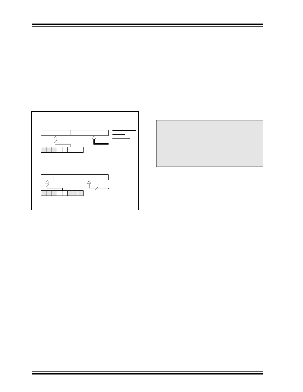
4.3 PCL and PCLATH
The program counter (PC) is 13-bits wide. The low b yte
comes from the PCL register, which is a readable and
writable register. The high byte (PC<12:8>) is not
directly readable or writable and comes from PCLATH.
On any reset, the PC is cleared. Figure 4-10 shows the
two situations for the loading of the PC. The upper
example in the figure shows how the PC is loaded on a
write to PCL (PCLA TH<4:0> → PCH). The lower e xample in the figure shows how the PC is loaded during a
CALL or GOTO instruction (PCLATH<4:3> → PCH).
FIGURE 4-10: LOADING OF PC IN
DIFFERENT SITUATIONS
PCH PCL
12 8 7 0
PC
PCLA TH<4:0>
5
PCLA TH
PCH PCL
12 11 10 0
PC
2
8 7
PCLATH<4:3>
PCLATH
11
4.3.1 COMPUTED GOTO A computed GOTO is accomplished by adding an off-
set to the program counter (ADDWF PCL). When doing a
table read using a computed GOTO method, care
should be exercised if the table location crosses a PCL
memory boundary (each 256 byte block). Refer to the
application note
“Implementing a Table Read"
8
Instr
uction with
PCL as
Destination
ALU result
GOTO, CALL
Opcode <10:0>
(AN556).
4.3.2 STACK The PIC12CE67X family has an 8 level deep x 13-bit
wide hardware stack. The stack space is not part of
either program or data space and the stack pointer is
not readable or writable. The PC is PUSHed onto the
stack when a CALL instruction is executed or an interrupt causes a branch. The stack is POPed in the event
of a RETURN, RETLW or a RETFIE instruction execution.
PCLA TH is not affected by a PUSH or POP operation.
The stack operates as a circular buffer . This means that
after the stack has been PUSHed eight times, the ninth
push overwrites the value that was stored from the first
push. The tenth push overwrites the second push (and
so on).
Note 1: There are no status bits to indicate stack
overflow or stack underflow conditions.
Note 2: There are no instructions/mnemonics
called PUSH or POP. These are actions
that occur from the execution of the CALL,
RETURN, RETLW, and RETFIE instructions, or the vectoring to an interrupt
address.
4.4 Program Memory Paging
The PIC12CE67X ignores both paging bits
PCLATH<4:3>, which are used to access program
memory when more than one page is available. The
use of PCLATH<4:3> as general purpose read/write
bits for the PIC12CE67X is not recommended since
this may affect upward compatibility with future products.
DS40181A-page 22 Preliminary 1998 Microchip Technology Inc.
PIC12CE67X
4.5 Indirect Addressing, INDF and FSR
Registers
The INDF register is not a physical register. Addressing
the INDF register will cause indirect addressing.
Indirect addressing is possible by using the INDF register. Any instruction using the INDF register actually
accesses the register pointed to by the File Select Register, FSR. Reading the INDF register itself indirectly
(FSR = '0') will read 00h. Writing to the INDF register
indirectly results in a no-operation (although status bits
may be affected). An effective 9-bit address is obtained
by concatenating the 8-bit FSR register and the IRP bit
(STA TUS<7>), as shown in Figure 4-11. However, IRP
is not used in the PIC12CE67X.
A simple program to clear RAM locations 20h-2Fh
using indirect addressing is shown in Example 4-1.
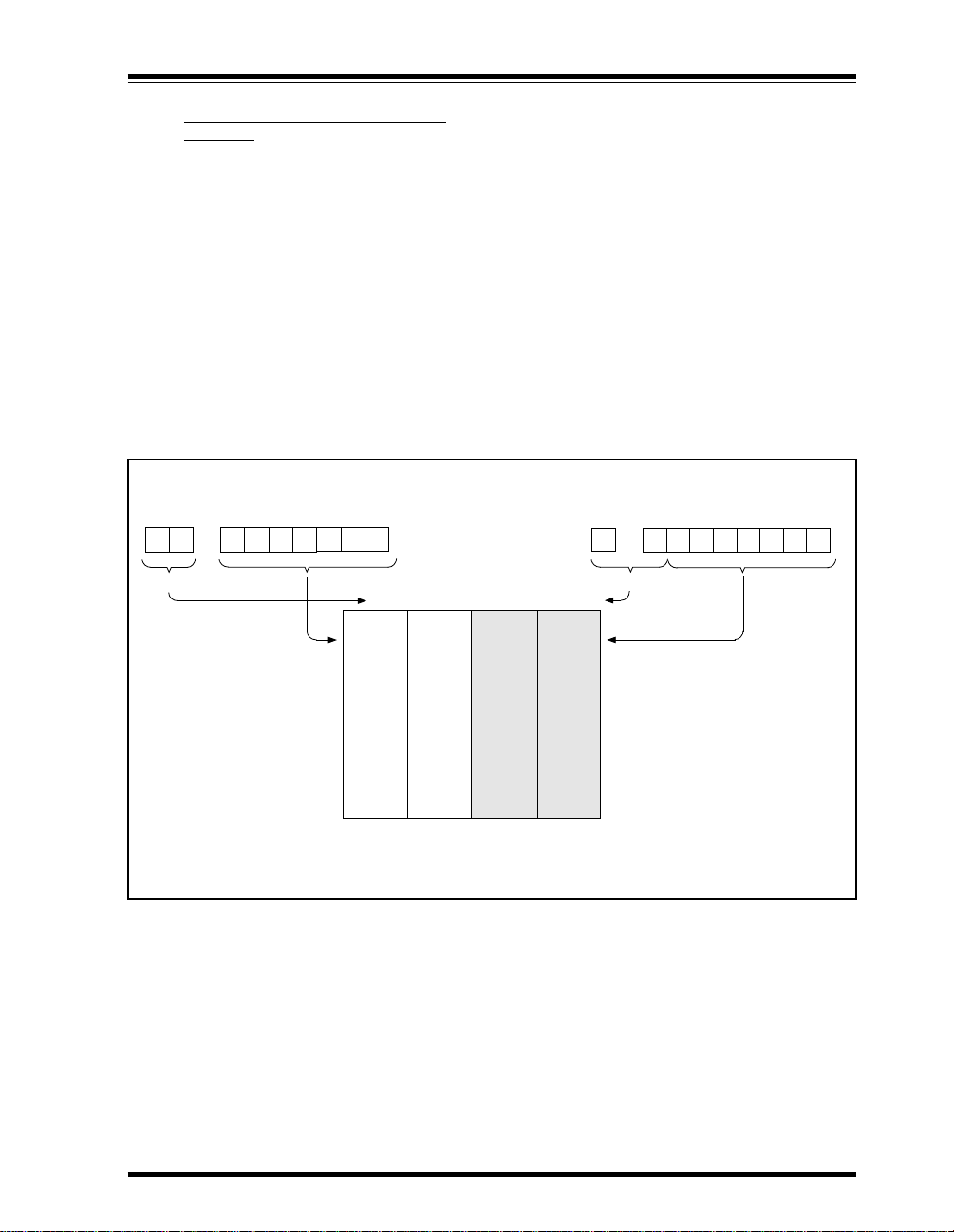
FIGURE 4-11: DIRECT/INDIRECT ADDRESSING
(1)
RP1 RP0 6
bank select location select
from opcode
00h
0
00 01 10 11
EXAMPLE 4-1: INDIRECT ADDRESSING
movlw 0x20 ;initialize pointer
movwf FSR ;to RAM
NEXT clrf INDF ;clear INDF register
incf FSR,F ;inc pointer
btfss FSR,4 ;all done?
goto NEXT ;no clear next
CONTINUE
: ;yes continue
Indirect AddressingDirect Addressing
(1)
IRP
bank select
00h
7
FSR register
location select
0
Data
Memory
7Fh
not used
7Fh
Bank 0 Bank 1 Bank 2 Bank 3
For register file map detail see Figure 4-2.
Note 1: The RP1 and IRP bits are reserved, always maintain these bits clear.
1998 Microchip Technology Inc. Preliminary DS40181A-page 23

PIC12CE67X
NOTES:
DS40181A-page 24 Preliminary 1998 Microchip Technology Inc.
PIC12CE67X
5.0 I/O PORT
As with any other register, the I/O register can be
written and read under program control. However,
read instructions (e.g., MOVF GPIO,W) always read the
I/O pins independent of the pin’s input/output modes.
On RESET, all I/O ports are defined as input (inputs
are at hi-impedance) since the I/O control registers are
all set.
5.1 GPIO
GPIO is an 8-bit I/O register. Only the low order 6 bits
are used (GP5:GP0). Bits 6 and 7 (SDA and SCL) are
used by the EEPROM peripheral. Refer to Section 6.0
and Appendix A for use of SDA and SCL. Please note
that GP3 is an input only pin. The configuration word
can set several I/O’s to alternate functions. When
acting as alternate functions the pins will read as ‘0’
during port read. Pins GP0, GP1, and GP3 can be
configured with weak pull-ups and also with interrupt
on change. The interrupt on change and weak pull-up
functions are not pin selectable. If pin 4 is configured
as MCLR
change for this pin is not set and GP3 will read as '0'.
Interrupt on change is enabled by setting INTCON<3>.
Note that external oscillator use overrides the GPIO
functions on GP4 and GP5.
5.2 TRIS Register
This register controls the data direction for GPIO. A '1'
from a TRIS register bit puts the corresponding output
driver in a hi-impedance mode. A '0' puts the contents
of the output data latch on the selected pins, enabling
the output buffer. The exceptions are GP3 which is
input only and its TRIS bit will always read as '1'.
Upon reset, the TRIS register is all '1's, making all pins
inputs.
, the weak pull-up is always on. Interrupt on
Note: A read of the ports reads the pins, not the
output data latches. That is, if an output
driver on a pin is enabled and driven high,
but the external system is holding it low, a
read of the port will indicate that the pin is
low.
5.3 I/O Interfacing
The equivalent circuit for an I/O port pin is shown in
Figure 5-2. All port pins, except GP3 which is input
only, may be used for both input and output
operations. For input operations these ports are nonlatching. Any input must be present until read by an
input instruction (e.g., MOVF GPIO,W). The outputs are
latched and remain unchanged until the output latch is
rewritten. To use a port pin as output, the
corresponding direction control bit in TRIS must be
cleared (= 0). For use as an input, the corresponding
TRIS bit must be set. Any I/O pin (except GP3) can be
programmed individually as input or output.
Note: On a Power-on Reset, GP0, GP1, GP2,
GP4 are configured as analog inputs and
read as '0'.
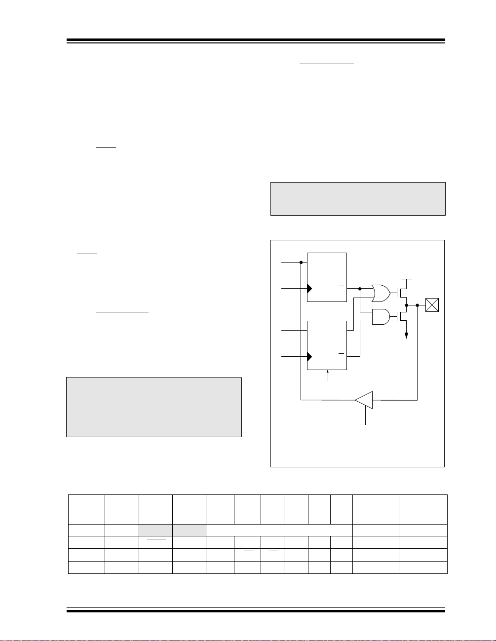
FIGURE 5-1: EQUIVALENT CIRCUIT
FOR A SINGLE I/O PIN
Data
Bus
WR
Port
W
Reg
TRIS ‘f’
Note 1: I/O pins have protection diodes to VDD and VSS.
GP3 is input only with no data latch and no
output drivers.
Data
Latch
CK
TRIS
Latch
CK
Reset
QD
VDD
Q
QD
Q
RD Port
P
N
VSS
I/O
pin
(1)
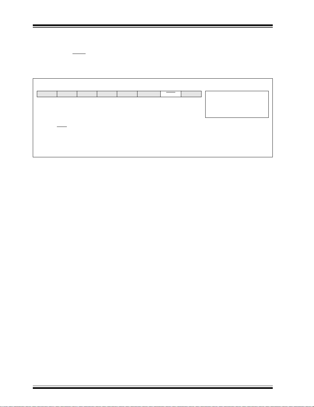
TABLE 5-1: SUMMARY OF PORT REGISTERS
Value on
Address Name Bit 7 Bit 6 Bit 5 Bit 4 Bit 3 Bit 2 Bit 1 Bit 0
85h TRIS
81h OPTION GPPU INTEDG T0CS T0SE PSA PS2 PS1 PS0 1111 1111 1111 1111
03h STATUS
05h GPIO SCL SDA GP5 GP4 GP3 GP2 GP1 GP0 11xx xxxx 11uu uuuu
Legend: Shaded cells not used by Port Registers, read as ‘0’, — = unimplemented, read as '0', x = unknown, u = unchanged,
q = see tables in Section 9.4 for possible values.
Note 1: The IRP and RP1 bits are reserved on the PIC12CE67X, always maintain these bits clear.
1998 Microchip Technology Inc. Preliminary DS40181A-page 25
— — GPIO Data Direction Register --11 1111 --11 1111
IRP
(1)
RP1
(1)
RP0 TO PD Z DC C 0001 1xxx 000q quuu
Power-on
Reset
Value on
all other
Resets
PIC12CE67X
5.4 I/O Programming Considerations
5.4.1 BI-DIRECTIONAL I/O PORTS Any instruction which writes, operates internally as a
read followed by a write operation. The BCF and BSF
instructions, for example, read the register into the
CPU, ex ecute the bit operation and write the result back
to the register. Caution must be used when these
instructions are applied to a port with both inputs and
outputs defined. For example, a BSF operation on bit5
of GPIO will cause all eight bits of GPIO to be read into
the CPU. Then the BSF operation takes place on bit5
and GPIO is written to the output latches. If another bit
of GPIO is used as a bi-directional I/O pin (e.g., bit0)
and it is defined as an input at this time, the input signal
present on the pin itself would be read into the CPU
and rewritten to the data latch of this particular pin,
overwriting the previous content. As long as the pin
stays in the input mode, no problem occurs. However,
if bit0 is switched to an output, the content of the data
latch may now be unknown.
Reading the port register, reads the values of the port
pins. Writing to the port register writes the value to the
port latch. When using read-modify-write instructions
(ex. BCF, BSF , etc.) on a port, the value of the port pins
is read, the desired operation is done to this value, and
this value is then written to the port latch.
FIGURE 5-2: SUCCESSIVE I/O OPERATION
Example 5-1 shows the effect of two sequential read-
modify-write instructions on an I/O port.
EXAMPLE 5-1: READ-MODIFY-WRITE
INSTRUCTIONS ON AN
I/O PORT
;Initial GPIO Settings
; GPIO<5:3> Inputs
; GPIO<2:0> Outputs
;
; GPIO latch GPIO pins
; ---------- --------- BCF GPIO, 5 ;--01 -ppp --11 pppp
BCF GPIO, 4 ;--10 -ppp --11 pppp
MOVLW 007h ;
TRIS GPIO ;--10 -ppp --11 pppp
;
;Note that the user may have expected the pin
;values to be --00 pppp. The 2nd BCF caused
;GP5 to be latched as the pin value (High).
A pin actively outputting a Low or High should not be
driven from external devices at the same time in order
to change the level on this pin (“wired-or”, “wired-and”).
The resulting high output currents may damage the
chip.
Q4
Q3
Q1 Q2
Instruction
fetched
GP5:GP0
Instruction
executed
DS40181A-page 26 Preliminary 1998 Microchip Technology Inc.
PC PC + 1 PC + 2
MOVWF GPIO
Q1 Q2
MOVF GPIO,W
MOVWF GPIO
Q3
Port pin
written here
(Write to
GPIO)
Q4
Q1 Q2
MOVF GPIO,W
Q3
NOP
Port pin
sampled here
(Read
GPIO)
Q4
Q1 Q2
Q3
PC + 3
NOP
NOP
Q4
This example shows a write to GPIO followed
by a read from GPIO.
Data setup time = (0.25 TCY – TPD)
where: TCY = instruction cycle.
TPD = propagation delay
Therefore, at higher clock frequencies, a
write followed by a read may be problematic.

PIC12CE67X
6.0 EEPROM PERIPHERAL
OPERATION
The PIC12CE673 and PIC12CE674 each have 16
bytes of EEPROM data memory. The EEPROM memory has an endurance of 1,000,000 erase/write cycles
and a data retention of greater than 40 years. The
EEPROM data memory supports a bi-directional 2-wire
bus and data transmission protocol. These two-wires
are serial data (SDA) and serial clock (SCL), that are
mapped to bit6 and bit7, respectively, of the GPIO register (SFR 06h). Unlike the GP0-GP5 that are connected to the I/O pins, SDA and SCL are only
connected to the internal EEPROM peripheral. For
most applications, all that is required is calls to the following functions:
; Byte_Write: Byte write routine
; Inputs: EEPROM Address EEADDR
; EEPROM Data EEDATA
; Outputs: Return 01 in W if OK, else
return 00 in W
;
; Read_Current: Read EEPROM at address
currently held by EE device.
; Inputs: NONE
; Outputs: EEPROM Data EEDATA
; Return 01 in W if OK, else
return 00 in W
;
; Read_Random: Read EEPROM byte at supplied
address
; Inputs: EEPROM Address EEADDR
; Outputs: EEPROM Data EEDATA
; Return 01 in W if OK,
else return 00 in W
The code for these functions is not yet determined, but
will be available on our web site (www.microchip.com)
when it is completed. The code will be accessed by
either including the source code FLASH67X.INC or by
linking FLASH67X.ASM.
6.0.1 SERIAL DATA
SDA is a bi-directional pin used to transfer addresses
and data into and data out of the device.
For normal data transfer SDA is allo wed to change only
during SCL low. Changes during SCL high are
reserved for indicating the START and STOP conditions.
6.0.2 SERIAL CLOCK
This SCL input is used to synchronize the data transf er
from and to the EEPROM.
6.1 BUS CHARACTERISTICS
The following bus protocol is to be used with the
EEPROM data memory. In this section, the term “processor” is used to denote the portion of the
PIC12CE67X that interfaces to the EEPROM via software.
• Data transfer may be initiated only when the bus
is not busy.
During data transfer, the data line must remain stable
whenever the clock line is HIGH. Changes in the data
line while the clock line is HIGH will be interpreted as a
START or STOP condition.
Accordingly, the following bus conditions have been
defined (Figure 6-1).
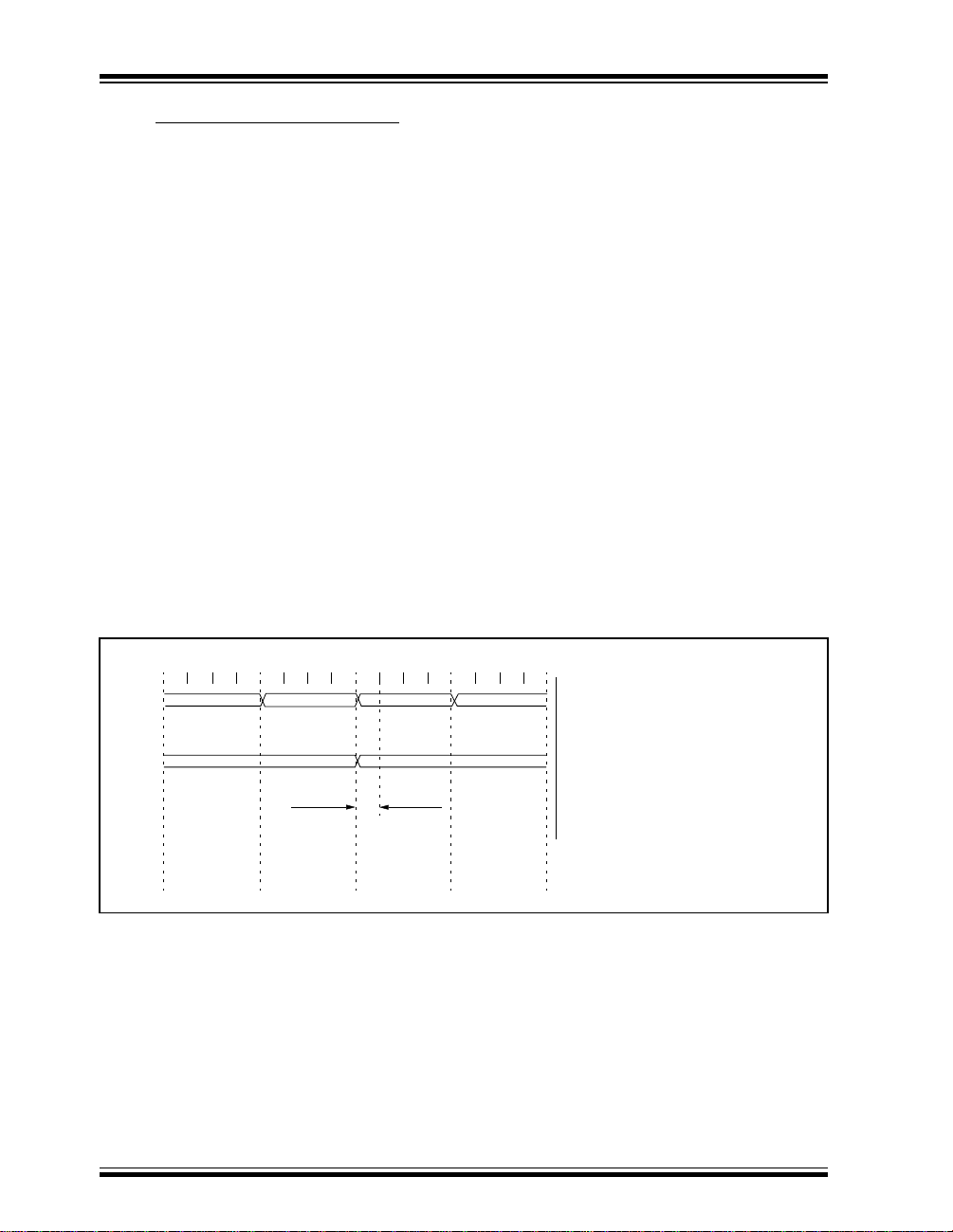
6.1.1 BUS NOT BUSY (A)
Both data and clock lines remain HIGH.
6.1.2 START DATA TRANSFER (B)
A HIGH to LOW transition of the SDA line while the
clock (SCL) is HIGH determines a ST AR T condition. All
commands must be preceded by a START condition.
6.1.3 STOP DATA TRANSFER (C)
A LOW to HIGH transition of the SDA line while the
clock (SCL) is HIGH determines a STOP condition. All
operations must be ended with a STOP condition.
6.1.4 DATA VALID (D)
The state of the data line represents valid data when,
after a START condition, the data line is stable for the
duration of the HIGH period of the clock signal.
The data on the line must be changed during the LOW
period of the clock signal. There is one bit of data per
clock pulse.
Each data transfer is initiated with a START condition
and terminated with a STOP condition. The number of
the data bytes transferred between the START and
STOP conditions is determined by the processor
device and is theoretically unlimited.
6.1.5 ACKNOWLEDGE
The EEPROM, when addressed, will generate an
acknowledge after the reception of each byte. The processor must generate an extra clock pulse which is
associated with this acknowledge bit.
Note: Acknowledge bits are not generated if an
internal programming cycle is in progress.
The device that acknowledges has to pull down the
SDA line during the acknowledge clock pulse in such a
way that the SDA line is stable LOW during the HIGH
period of the acknowledge related clock pulse. Of
course, setup and hold times must be taken into
account. The processor must signal an end of data to
the EEPROM by not generating an acknowledge bit on
the last byte that has been clocked out of the EEPROM.
In this case, the EEPROM must leave the data line
HIGH to enable the processor to generate the STOP
condition (Figure 6-2).
1998 Microchip Technology Inc. Preliminary DS40181A-page 27
PIC12CE67X
FIGURE 6-1: DATA TRANSFER SEQUENCE ON THE SERIAL BUS
SCL
SDA
(A)
START
CONDITION
(C)
ADDRESS OR
ACKNOWLEDGE
VALID
(B)
FIGURE 6-2: ACKNOWLEDGE TIMING
SCL
SDA
Data from transmitter
Transmitter must release the SDA line at this point
allowing the Receiver to pull the SDA line low to
acknowledge the previous eight bits of data.
DATA
ALLOWED
TO CHANGE
Acknowledge
(D)
Bit
987654321 1 2 3
Data from transmitter
Receiver must release the SDA line at this point
so the Transmitter can continue sending data.
STOP
CONDITION
(A)(C)
6.2 Device Addressing
After generating a START condition, the processor
FIGURE 6-3: CONTROL BYTE FORMAT
Read/Wr
ite Bit
transmits a control byte consisting of a EEPROM
address and a Read/Wr
ite bit that indicates what type
of operation is to be performed. The EEPROM address
Device Select
Bits
Don’t Care
Bits
consists of a 4-bit device code (1010) followed b y three
don't care bits.
1 0 1 0 X X XS ACKR/W
The last bit of the control byte determines the operation
to be performed. When set to a one a read operation is
selected, and when set to a zero a write operation is
selected. (Figure 6-3). The bus is monitored for its cor-
Start Bit
EEPROM Address
Acknowledge Bit
responding EEPROM address all the time. It generates
an acknowledge bit if the EEPROM address was true
and it is not in a programming mode.
DS40181A-page 28 Preliminary 1998 Microchip Technology Inc.
PIC12CE67X
6.3 WRITE OPERATIONS
6.3.1 BYTE WRITE Following the start signal from the processor, the
device code (4 bits), the don't care bits (3 bits), and the
R/W
bit (which is a logic low) are placed onto the bus
by the processor. This indicates to the addressed
EEPROM that a byte with a word address will follow
after it has generated an acknowledge bit during the
ninth clock cycle. Therefore, the next byte transmitted
by the processor is the word address and will be written
into the address pointer. Only the lower four address
bits are used by the device, and the upper four bits are
don’t cares. The address byte is acknowledgeable and
the processor will then transmit the data word to be
written into the addressed memory location. The memory acknowledges again and the processor generates
a stop condition. This initiates the internal write cycle,
and during this time will not generate acknowledge signals (Figure 6-5). After a byte write command, the internal address counter will not be incremented and will
point to the same address location that was just written.
If a stop bit is transmitted to the device at any point in
the write command sequence before the entire
sequence is complete, then the command will abort
and no data will be written. If more than 8 data bits are
transmitted before the stop bit is sent, then the device
will clear the previously loaded byte and begin loading
the data buffer again. If more than one data byte is
transmitted to the device and a stop bit is sent before a
full eight data bits have been transmitted, then the write
command will abort and no data will be written. The
EEPROM memory employs a V
circuit which disables the internal erase/write logic if
the V
CC is below minimum VDD.
CC threshold detector
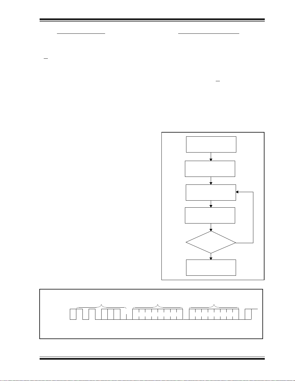
6.4 ACKNOWLEDGE POLLING
Since the EEPROM will not acknowledge during a write
cycle, this can be used to determine when the cycle is
complete (this feature can be used to maximize bus
throughput). Once the stop condition for a write command has been issued from the processor, the device
initiates the internally timed write cycle. ACK polling
can be initiated immediately. This involves the processor sending a start condition followed by the control
byte for a write command (R/W
= 0). If the device is still
busy with the write cycle, then no ACK will be returned.
If no ACK is returned, then the start bit and control byte
must be re-sent. If the cycle is complete, then the
device will return the ACK and the processor can then
proceed with the next read or write command. See
Figure 6-4 for flow diagram.
FIGURE 6-4: ACKNOWLEDGE POLLING
FLOW
Send
Write Command
Send Stop
Condition to
Initiate Write Cycle
Send Start
Send Control Byte
with R/W = 0
Did EEPROM
Acknowledge
(ACK = 0)?
NO
YES
Next
Operation
FIGURE 6-5: BYTE WRITE
S
BUS ACTIVITY
PROCESSOR
SDA LINE
BUS ACTIVITY
X = Don’t Care Bit
1998 Microchip Technology Inc. Preliminary DS40181A-page 29
T
A
R
T
S
CONTROL
BYTE
1 0 X1 0 XX X
0
A
C
K
ADDRESS
X X X
WORD
DATA
A
C
K
S
T
O
P
P
A
C
K
PIC12CE67X
6.5 READ OPERATIONS
Read operations are initiated in the same way as write
operations with the exception that the R/W
bit of the
EEPROM address is set to one. There are three basic
types of read operations: current address read, random
read, and sequential read.
6.5.1 CURRENT ADDRESS READ It contains an address counter that maintains the
address of the last word accessed, internally incremented by one. Therefore, if the previous read access
was to address n, the next current address read operation would access data from address n + 1. Upon
receipt of the EEPROM address with the R/W
bit set to
one, the EEPROM issues an acknowledge and transmits the eight bit data word. The processor will not
acknowledge the transfer but does generate a stop
condition and the EEPROM discontinues transmission
(Figure 6-6).
6.5.2 RANDOM READ Random read operations allow the processor to access
any memory location in a random manner. To perform
this type of read operation, first the word address must
be set. This is done b y sending the word address to the
FIGURE 6-6: CURRENT ADDRESS READ
S
BUS ACTIVITY
PROCESSOR
SDA LINE
BUS ACTIVITY
X = Don’t Care Bit
T
A
R
T
S
FIGURE 6-7: RANDOM READ
S
BUS ACTIVITY
PROCESSOR
SDA LINE
BUS ACTIVITY
X = Don’t Care Bit
T
CONTROL
A
BYTE
R
T
S 1 10 0 X X X 0
ADDRESS (n)
X X X X
A
C
K
FIGURE 6-8: SEQUENTIAL READ
BUS ACTIVITY
PROCESSOR
SDA LINE
BUS ACTIVITY
CONTROL
BYTE
DATA n DATA n + 1 DATA n + 2 DATA n + X
A
C
K
A
C
K
EEPROM as part of a write operation. After the word
address is sent, the processor generates a start condition following the acknowledge. This terminates the
write operation, but not before the internal address
pointer is set. Then the processor issues the control
byte again but with the R/W
issue an acknowledge and transmits the eight bit data
word. The processor will not acknowledge the transfer
but does generate a stop condition and the EEPROM
discontinues transmission (Figure 6-7). After this command, the internal address counter will point to the
address location following the one that was just read.
6.5.3 SEQUENTIAL READ
Sequential reads are initiated in the same way as a ran-
dom read except that after the device transmits the first
data byte, the processor issues an acknowledge as
opposed to a stop condition in a random read. This
directs the EEPROM to transmit the next sequentially
addressed 8-bit word (Figure 6-8).
To provide sequential reads, it contains an internal
address pointer which is incremented by one at the
completion of each read operation. This address
pointer allows the entire memory contents to be serially
read during one operation.
CONTROL
BYTE
1 10 0 X X X 1
WORD
A
C
K
A
C
DATA
K
S
T
CONTROL
A
BYTE
R
T
S 1 10 0 X X X 1
A
C
K
bit set to a one. It will then
S
T
O
P
P
N
O
A
C
K
A
C
DATA (n)
K
A
C
K
S
T
O
P
P
N
O
A
C
K
S
T
O
P
P
N
O
A
C
K
DS40181A-page 30 Preliminary 1998 Microchip Technology Inc.

PIC12CE67X
7.0 TIMER0 MODULE
The Timer0 module timer/counter has the following features:
• 8-bit timer/counter
• Readable and writable
• 8-bit software programmable prescaler
• Internal or external clock select
• Interrupt on overflow from FFh to 00h
• Edge select for external clock
Figure 7-1 is a simplified block diagram of the Timer0
module.
Timer mode is selected by clearing bit T0CS
(OPTION<5>). In timer mode, the Timer0 module will
increment every instruction cycle (without prescaler). If
the TMR0 register is written, the increment is inhibited
for the following two instruction cycles (Figure 7-2 and
Figure 7-3). The user can work around this by writing
an adjusted value to the TMR0 register.
Counter mode is selected by setting bit T0CS
(OPTION<5>). In counter mode, Timer0 will increment
either on every rising or falling edge of pin RA4/T0CKI.
The incrementing edge is determined by the Timer0
Source Edge Select bit T0SE (OPTION<4>). Clearing
FIGURE 7-1: TIMER0 BLOCK DIAGRAM
FOSC/4
GP2/T0CKI/
AN2
T0SE
Note 1: T0CS, T0SE, PSA, PS2:PS0 (OPTION<5:0>).
2: The prescaler is shared with Watchdog Timer (refer to Figure 7-6 for detailed block diagram).
0
1
T0CS
Programmable
Prescaler
3
PS2, PS1, PS0
bit T0SE selects the rising edge. Restrictions on the
external clock input are discussed in detail in
Section 7.2.
The prescaler is mutually exclusively shared between
the Timer0 module and the Watchdog Timer. The prescaler assignment is controlled in software by control bit
PSA (OPTION<3>). Clearing bit PSA will assign the
prescaler to the Timer0 module. The prescaler is not
readable or writable. When the prescaler is assigned to
the Timer0 module, prescale values of 1:2, 1:4, ...,
1:256 are selectable. Section 7.3 details the operation
of the prescaler.
7.1 Timer0 Interrupt
The TMR0 interrupt is generated when the TMR0 register overflows from FFh to 00h. This overflow sets bit
T0IF (INTCON<2>). The interrupt can be masked by
clearing bit T0IE (INTCON<5>). Bit T0IF must be
cleared in software by the Timer0 module interrupt service routine before re-enabling this interrupt. The TMR0
interrupt cannot awaken the processor from SLEEP
since the timer is shut off during SLEEP. See Figure 74 for Timer0 interrupt timing.
Data bus
TMR0
8
Set interrupt
flag bit T0IF
on overflow
1
0
PSA
PSout
Sync with
Internal
clocks
(2 cycle delay)
PSout
FIGURE 7-2: TIMER0 TIMING: INTERNAL CLOCK/NO PRESCALE
PC
(Program
Counter)
Instruction
Fetch
TMR0
Instruction
Executed
1998 Microchip Technology Inc. Preliminary DS40181A-page 31
Q1 Q2 Q3 Q4
T0
Q1 Q2 Q3 Q4 Q1 Q2 Q3 Q4 Q1 Q2 Q3 Q4 Q1 Q2 Q3 Q4 Q1 Q2 Q3 Q4 Q1 Q2 Q3 Q4 Q1 Q2 Q3 Q4
PC-1
PC PC+1 PC+2 PC+3 PC+4 PC+5 PC+6
MOVWF TMR0
T0+1 T0+2 NT0 NT0 NT0 NT0+1 NT0+2
MOVF TMR0,W MOVF TMR0,W MOVF TMR0,W MOVF TMR0,W MOVF TMR0,W
Write TMR0
executed
Read TMR0
reads NT0
Read TMR0
reads NT0
Read TMR0
reads NT0
Read TMR0
reads NT0 + 1
Read TMR0
reads NT0 + 2
T0
PIC12CE67X
FIGURE 7-3: TIMER0 TIMING: INTERNAL CLOCK/PRESCALE 1:2
PC
(Program
Counter)
Instruction
Fetch
TMR0
Instruction
Execute
Q1 Q2 Q3 Q4
T0 NT0+1
Q1 Q2 Q3 Q4 Q1 Q2 Q3 Q4 Q1 Q2 Q3 Q4 Q1 Q2 Q3 Q4 Q1 Q2 Q3 Q4 Q1 Q2 Q3 Q4 Q1 Q2 Q3 Q4
PC-1
PC PC+1 PC+2 PC+3 PC+4 PC+5 PC+6
MOVWF TMR0
MOVF TMR0,W MOVF TMR0,W MOVF TMR0,W MOVF TMR0,W MOVF TMR0,W
T0+1
Write TMR0
executed
FIGURE 7-4: TIMER0 INTERRUPT TIMING
Q2Q1 Q3 Q4Q2Q1 Q3 Q4 Q2Q1 Q3 Q4 Q2Q1 Q3 Q4 Q2Q1 Q3 Q4
OSC1
CLKOUT(3)
Timer0
T0IF bit
(INTCON<2>)
GIE bit
(INTCON<7>)
UCTION
INSTR
LOW
F
Instruction
fetched
Instruction
executed
FEh
1
PC
PC
Inst (PC)
Inst (PC-1)
FFh 00h 01h 02h
1
PC +1 PC +1 0004h 0005h
Inst (PC+1)
Inst (PC)
Read TMR0
reads NT0
NT0
Read TMR0
reads NT0
Read TMR0
reads NT0
Read TMR0
reads NT0
Inst (0004h) Inst (0005h)
Read TMR0
reads NT0 + 1
Inst (0004h)Dummy cycle Dummy cycle
Note 1: Interrupt flag bit T0IF is sampled here (every Q1).
2: Interrupt latency = 4Tcy where Tcy = instruction cycle time.
3: CLKOUT is available only in RC oscillator mode.
DS40181A-page 32 Preliminary 1998 Microchip Technology Inc.

PIC12CE67X
7.2 Using Timer0 with an External Clock
When an external clock input is used for Timer0, it must
meet certain requirements. The requirements ensure
the external clock can be synchronized with the internal
phase clock (T
incrementing of Timer0 after synchronization.
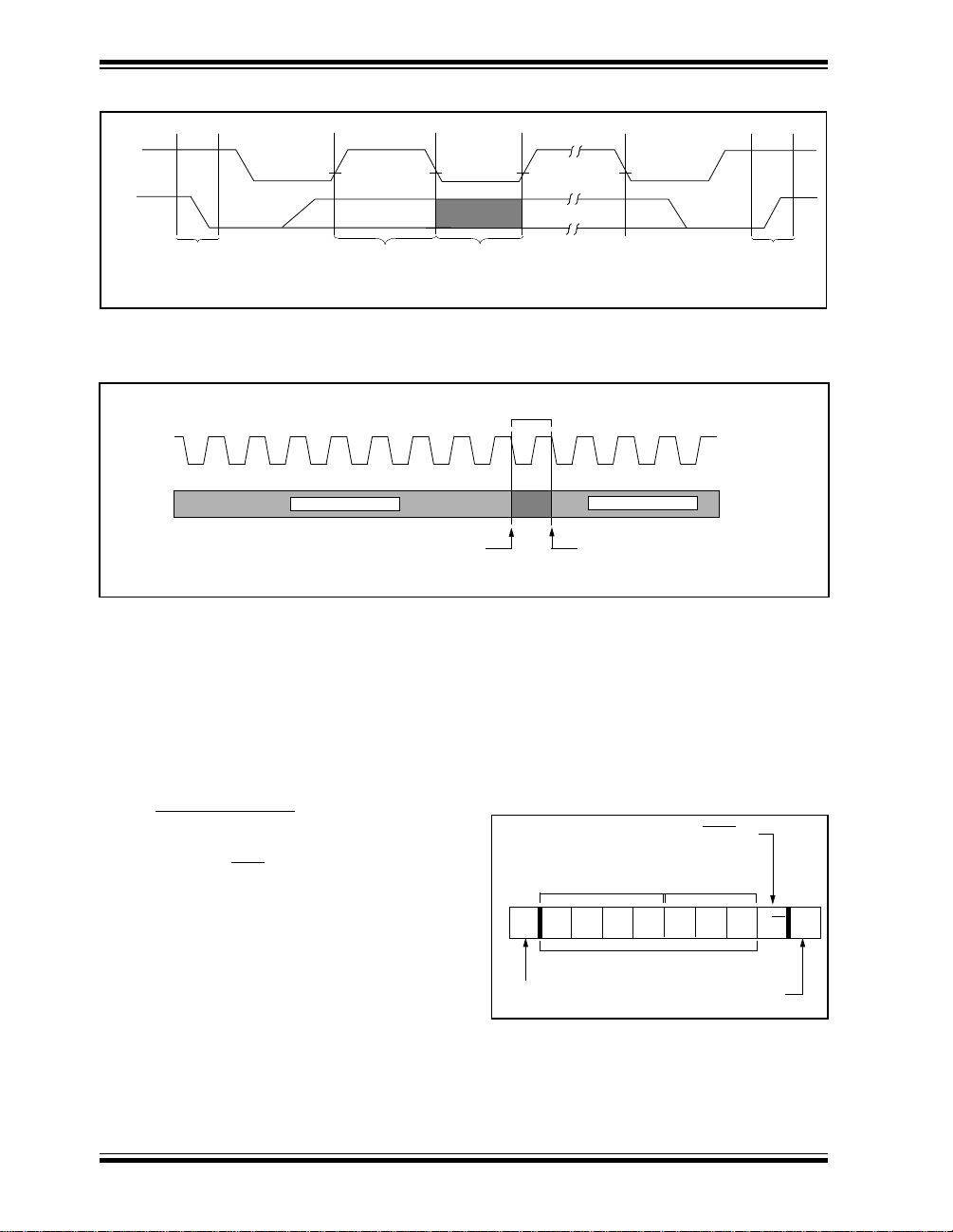
7.2.1 EXTERNAL CLOCK SYNCHRONIZATION When no prescaler is used, the external clock input is
the same as the prescaler output. The synchronization
of T0CKI with the internal phase clocks is accomplished by sampling the prescaler output on the Q2 and
Q4 cycles of the internal phase clocks (Figure 7-5).
Therefore, it is necessary for T0CKI to be high for at
least 2Tosc (and a small RC delay of 20 ns) and low for
at least 2T osc (and a small RC delay of 20 ns). Refer to
the electrical specification of the desired device.
OSC). Also, there is a delay in the actual
caler so that the prescaler output is symmetrical. For
the external clock to meet the sampling requirement,
the ripple-counter must be taken into account. Therefore, it is necessary for T0CKI to have a period of at
least 4Tosc (and a small RC delay of 40 ns) divided by
the prescaler value. The only requirement on T0CKI
high and low time is that they do not violate the minimum pulse width requirement of 10 ns. Ref er to parameters 40, 41 and 42 in the electrical specification of the
desired device.
7.2.2 TMR0 INCREMENT DELAY Since the prescaler output is synchronized with the
internal clocks, there is a small delay from the time the
external clock edge occurs to the time the Timer0 module is actually incremented. Figure 7-5 shows the delay
from the external clock edge to the timer incrementing.
When a prescaler is used, the external clock input is
divided by the asynchronous ripple-counter type pres-
FIGURE 7-5: TIMER0 TIMING WITH EXTERNAL CLOCK
Q1 Q2 Q3 Q4 Q1 Q2 Q3 Q4 Q1 Q2 Q3 Q4 Q1 Q2 Q3 Q4
External Clock Input or
Prescaler output
External Clock/Prescaler
Output after sampling
Increment Timer0 (Q4)
(2)
Timer0
(3)
(1)
T0 T0 + 1 T0 + 2
Small pulse
misses sampling
Note 1: Delay from clock input change to Timer0 increment is 3Tosc to 7Tosc. (Duration of Q = Tosc).
Therefore, the error in measuring the interval between two edges on Timer0 input = ±4Tosc max.
2: External clock if no prescaler selected, Prescaler output otherwise.
3: The arrows indicate the points in time where sampling occurs.
1998 Microchip Technology Inc. Preliminary DS40181A-page 33
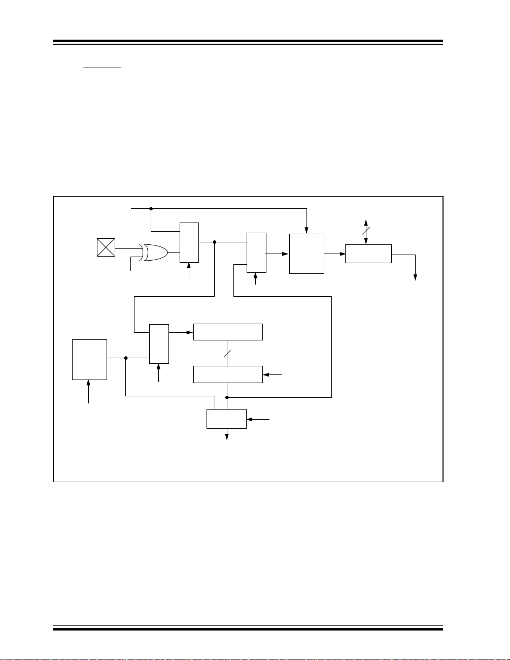
PIC12CE67X
7.3 Prescaler
An 8-bit counter is available as a prescaler for the
Timer0 module, or as a postscaler for the Watchdog
Timer, respectively (Figure 7-6). For simplicity, this
counter is being referred to as “prescaler” throughout
this data sheet. Note that there is only one prescaler
available which is mutually e xclusiv ely shared betw een
the Timer0 module and the Watchdog Timer. Thus, a
The PSA and PS2:PS0 bits (OPTION<3:0>) determine
the prescaler assignment and prescale ratio.
When assigned to the Timer0 module, all instructions
writing to the TMR0 register (e.g. CLRF 1, MOVWF 1,
BSF 1,x....etc.) will clear the prescaler. When assigned
to WDT, a CLRWDT instruction will clear the prescaler
along with the Watchdog Timer. The prescaler is not
readable or writable.
prescaler assignment for the Timer0 module means
that there is no prescaler for the Watchdog Timer, and
vice-versa.
FIGURE 7-6: BLOCK DIAGRAM OF THE TIMER0/WDT PRESCALER
CLKOUT (=Fosc/4)
GP2/T0CKI/
AN2
Watchdog
Timer
T0SE
M
0
U
X
1
T0CS
0
M
U
1
X
PSA
8-bit Prescaler
8 - to - 1MUX
1
M
U
0
X
PSA
8
SYNC
2
Cycles
PS2:PS0
Data Bus
TMR0 reg
8
Set flag bit T0IF
on Overflow
M U X
WDT
Time-out
1
PSA
WDT Enable bit
Note: T0CS, T0SE, PSA, PS2:PS0 are (OPTION<5:0>).
DS40181A-page 34 Preliminary 1998 Microchip Technology Inc.
0

PIC12CE67X
7.3.1 SWITCHING PRESCALER ASSIGNMENT The prescaler assignment is fully under software con-
trol, i.e., it can be changed “on the fly” during program
execution.
Note: To avoid an unintended device RESET, the
following instruction sequence (shown in
Example 7-1) must be executed when
changing the prescaler assignment from
Timer0 to the WDT. This sequence must
be followed even if the WDT is disabled.
To change prescaler from the WDT to the Timer0 module use the sequence shown in Example 7-2.
EXAMPLE 7-2: CHANGING PRESCALER
(WDT→TIMER0)
CLRWDT ;Clear WDT and
;prescaler
BSF STATUS, RP0 ;Bank 1
MOVLW b'xxxx0xxx' ;Select TMR0, new
;prescale value and
MOVWF OPTION_REG ;clock source
BCF STATUS, RP0 ;Bank 0
EXAMPLE 7-1: CHANGING PRESCALER
(TIMER0→WDT)
BCF STATUS, RP0 ;Bank 0
CLRF TMR0 ;Clear TMR0 & Prescaler
BSF STATUS, RP0 ;Bank 1
CLRWDT ;Clears WDT
MOVLW b'xxxx1xxx' ;Select new prescale
MOVWF OPTION_REG ;value & WDT
BCF STATUS, RP0 ;Bank 0
TABLE 7-1: REGISTERS ASSOCIATED WITH TIMER0
Address Name Bit 7 Bit 6 Bit 5 Bit 4 Bit 3 Bit 2 Bit 1 Bit 0
01h TMR0 Timer0 module’s register xxxx xxxx uuuu uuuu
0Bh/8Bh INTCON GIE PEIE T0IE INTE GPIE T0IF INTF GPIF 0000 000x 0000 000u
81h OPTION GPPU INTEDG T0CS T0SE PSA PS2 PS1 PS0 1111 1111 1111 1111
85h TRIS — — TRIS5 TRIS4 TRIS3 TRIS2 TRIS1 TRIS0 --11 1111 --11 1111
Legend: x = unknown, u = unchanged, - = unimplemented locations read as '0'. Shaded cells are not used by Timer0.
Value on
POR
Value on
all other
Resets
1998 Microchip Technology Inc. Preliminary DS40181A-page 35

PIC12CE67X
NOTES:
DS40181A-page 36 Preliminary 1998 Microchip Technology Inc.

PIC12CE67X
8.0 ANALOG-TO-DIGITAL
CONVERTER (A/D) MODULE
The analog-to-digital (A/D) converter module has four
analog inputs.
The A/D allows conversion of an analog input signal to
a corresponding 8-bit digital number (refer to Application Note AN546 for use of A/D Converter). The output
of the sample and hold is the input into the converter,
which generates the result via successive approximation. The analog reference voltage is software selectable to either the device’ s positive supply v oltage (V
or the voltage level on the GP1/AN1/V
converter has a unique feature of being able to operate
while the device is in SLEEP mode.
REF pin. The A/D
DD)
The A/D module has three registers. These registers
are:
• A/D Result Register (ADRES)
• A/D Control Register 0 (ADCON0)
• A/D Control Register 1 (ADCON1)
The ADCON0 register, shown in Figure 8-1, controls
the operation of the A/D module. The ADCON1 register, shown in Figure 8-2, configures the functions of the
port pins. The port pins can be configured as analog
inputs (GP1 can also be a voltage reference) or as digital I/O.
Note: If the port pins are configured as analog
inputs (reset condition), reading the port
(MOVF GP,W) results in reading '0's.
FIGURE 8-1: ADCON0 REGISTER (ADDRESS 1Fh)
R/W-0 R/W-0 R/W-0 R/W-0 R/W-0 R/W-0 R/W-0 R/W-0
ADCS1 ADCS0
bit7 bit0
bit 7-6: ADCS1:ADCS0: A/D Conversion Clock Select bits
00 = F
01 = F
10 = F
11 = F
bit 5: Reserved
bit 4-3: CHS1:CHS0: Analog Channel Select bits
00 = channel 0, (GP0/AN0)
01 = channel 1, (GP1/AN1)
10 = channel 2, (GP2/AN2)
11 = channel 3, (GP4/AN3)
bit 2: GO/DONE
If ADON = 1
1 = A/D conversion in progress (setting this bit starts the A/D conversion)
0 = A/D conversion not in progress (This bit is automatically cleared by hardware when the A/D conver-
sion is complete)
bit 1: Reserved
bit 0: ADON: A/D On bit
1 = A/D converter module is operating
0 = A/D converter module is shutoff and consumes no operating current
r CHS1 CHS0 GO/DONE r ADON R = Readable bit
OSC/2
OSC/8
OSC/32
RC (clock derived from an RC oscillation)
: A/D Conversion Status bit
W =Writable bit
U =Unimplemented bit,
read as ‘0’
- n = Value at POR reset
1998 Microchip Technology Inc. Preliminary DS40181A-page 37

PIC12CE67X
FIGURE 8-2: ADCON1 REGISTER (ADDRESS 9Fh)
U-0 U-0 U-0 U-0 U-0 R/W-0 R/W-0 R/W-0
— — — — — PCFG2 PCFG1 PCFG0 R =Readable bit
bit7 bit0
bit 7-2: Unimplemented: Read as '0'
bit 1-0: PCFG2:PCFG0: A/D Port Configuration Control bits
W =Writable bit
U =Unimplemented
- n =Value at POR reset
bit, read as ‘0’
PCFG2:PCFG0 GP4 GP2 GP1 GP0 V
(1)
000
001 A A VREF A GP1
010 D A A A V
011 D A VREF A GP1
100 D D A A V
101 D D VREF A GP1
110 D D D A V
111 D D D D VDD
A = Analog input
D = Digital I/O
Note 1: Value on reset.
Note 2: Any instruction that reads a pin configured as an analog input will read a '0'.
A A A A VDD
REF
DD
DD
DD
DS40181A-page 38 Preliminary 1998 Microchip Technology Inc.

PIC12CE67X
The ADRES register contains the result of the A/D conversion. When the A/D conversion is complete, the
result is loaded into the ADRES register, the GO/DONE
bit (ADCON0<2>) is cleared, and A/D interrupt flag bit
ADIF (PIE1<6>) is set. The block diagrams of the A/D
module are shown in Figure 8-3.
After the A/D module has been configured as desired,
the selected channel must be acquired before the conversion is started. The analog input channels must
have their corresponding TRIS bits selected as an
input. To determine sample time, see Section 8.1. After
this acquisition time has elapsed the A/D conversion
can be started. The following steps should be followed
for doing an A/D conversion:
1. Configure the A/D module:
• Configure analog pins / voltage reference /
and digital I/O (ADCON1)
• Select A/D input channel (ADCON0)
• Select A/D conversion clock (ADCON0)
• Turn on A/D module (ADCON0)
FIGURE 8-3: A/D BLOCK DIAGRAM
VIN
(Input voltage)
A/D
Converter
VREF
(Reference
voltage)
PCFG2:PCFG0
2. Configure A/D interrupt (if desired):
• Clear ADIF bit
• Set ADIE bit
• Set GIE bit
3. Wait the required acquisition time.
4. Start conversion:
• Set GO/DONE
bit (ADCON0)
5. Wait for A/D conversion to complete, by either:
• Polling for the GO/DONE
bit to be cleared
OR
• Waiting for the A/D interrupt
6. Read A/D Result register (ADRES), clear bit
ADIF if required.
7. For next conversion, go to step 1 or step 2 as
required. The A/D conversion time per bit is
defined as T
AD. A minimum wait of 2TAD is
required before next acquisition starts.
CHS1:CHS0
11
10
01
00
DD
V
000 or
010 or
100 or
110 or
001 or
011 or
101
GP4/AN3
GP2/AN2
GP1/AN1/V
GP0/AN0
REF
1998 Microchip Technology Inc. Preliminary DS40181A-page 39

PIC12CE67X
8.1 A/D Sampling Requirements
For the A/D converter to meet its specified accuracy,
the charge holding capacitor (C
HOLD) must be allowed
to fully charge to the input channel voltage level. The
analog input model is shown in Figure 8-4. The source
impedance (R
S) and the internal sampling switch (RSS)
impedance directly affect the time required to charge
the capacitor C
impedance varies over the device voltage (V
HOLD. The sampling switch (RSS)
DD), see
Figure 8-4. The maximum recommended imped-
ance for analog sources is 10 kΩ. After the analog
input channel is selected (changed) this acquisition
must be done before the conversion can be started.
To calculate the minimum acquisition time, Equation 81 may be used. This equation assumes that 1/2 LSb
error is used (512 steps for the A/D). The 1/2 LSb error
is the maximum error allowed for the A/D to meet its
specified resolution.
EQUATION 8-1: A/D MINIMUM CHARGING
TIME
VHOLD = (VREF - (VREF/512)) • (1 - e
or
Tc = -(51.2 pF)(1 kΩ + RSS + RS) ln(1/511)
Example 8-1 shows the calculation of the minimum
required acquisition time T
based on the following system assumptions.
Rs = 10 k
Ω
1/2 LSb error
DD = 5V → Rss = 7 kΩ
V
Temp (system max.) = 50°C
HOLD = 0 @ t = 0
V
(-Tc/CHOLD(RIC + RSS + RS))
ACQ. This calculation is
Note 1: The reference voltage (VREF) has no
effect on the equation, since it cancels
itself out.
Note 2: The charge holding capacitor (C
HOLD) is
not discharged after each conversion.
Note 3: The maximum recommended impedance
for analog sources is 10 kΩ. This is
required to meet the pin leakage specification.
Note 4: After a conversion has completed, a
2.0 T
AD delay must complete before
acquisition can begin again. During this
time the holding capacitor is not connected to the selected A/D input channel.
EXAMPLE 8-1: CALCULATING THE
MINIMUM REQUIRED
SAMPLE TIME
TACQ = Amplifier Settling Time +
)
Holding Capacitor Charging Time +
Temperature Coefficient
ACQ = 5 µs + Tc + [(Temp - 25°C)(0.05 µs/°C)]
T
C = -CHOLD (RIC + RSS + RS) ln(1/512)
T
-51.2 pF (1 kΩ + 7 kΩ + 10 kΩ) ln(0.0020)
-51.2 pF (18 kΩ) ln(0.0020)
-0.921 µs (-6.2146)
5.724 µs
ACQ = 5 µs + 5.724 µs + [(50°C - 25°C)(0.05 µs/°C)]
T
10.724 µs + 1.25 µs
11.974 µs
FIGURE 8-4: ANALOG INPUT MODEL
VDD
RAx
Rs
VA
Legend CPIN
DS40181A-page 40 Preliminary 1998 Microchip Technology Inc.
CPIN
5 pF
= input capacitance
= threshold voltage
VT
= leakage current at the pin due to
I leakage
R
SS
C
various junctions
= interconnect resistance
IC
= sampling switch
= sample/hold capacitance (from DAC)
HOLD
VT = 0.6V
V
T = 0.6V
R
I leakage
± 500 nA
IC ≤ 1k
Sampling
Switch
SS
V
DD
SS
R
6V
5V
4V
3V
2V
CHOLD
= DAC capacitance
= 51.2 pF
SS
V
5 6 7 8 9 10 11
Sampling Switch
( kΩ )

PIC12CE67X
8.2 Selecting the A/D Conversion Clock
The A/D conversion time per bit is defined as TAD. The
A/D conversion requires 9.5 T
The source of the A/D conversion clock is software
selected. The four possible options for T
OSC
• 2T
• 8TOSC
• 32TOSC
• Precision internal 4 MHz oscillator
For correct A/D conversions, the A/D conversion clock
(T
AD) must be selected to ensure a minimum TAD time
of 1.6 µs.
Table 8-1 shows the resultant T
the device operating frequencies and the A/D clock
source selected.
AD per 8-bit conversion.
AD are:
AD times derived from
8.3 Configuring Analog Port Pins
The ADCON1 and TRIS registers control the operation
of the A/D port pins. The port pins that are desired as
analog inputs must have their corresponding TRIS bits
set (input). If the TRIS bit is cleared (output), the digital
output level (V
The A/D operation is independent of the state of the
CHS2:CHS0 bits and the TRIS bits.
Note 1: When reading the por t register, all pins
Note 2: Analog levels on any pin that is defined as
OH or VOL) will be converted.
configured as analog input channel will
read as cleared (a low level). Pins configured as digital inputs, will convert an analog input. Analog levels on a digitally
configured input will not affect the conversion accuracy.
a digital input (including the AN3:AN0
pins), may cause the input buffer to consume current that is out of the devices
specification.
TABLE 8-1: TAD vs. DEVICE OPERATING FREQUENCIES
AD Clock Source (TAD)
Operation ADCS1:ADCS0 4 MHz 1.25 MHz 333.33 kHz
OSC 00
2T
8T
OSC 01 2.0 µs 6.4 µs
500 ns
(2)
32TOSC 10 8.0 µs
Internal ADC RC Oscillator
(5)
11
2 - 6 µs
(1,4)
Note 1: The RC source has a typical TAD time of 4 µs.
2: These values violate the minimum required T
AD time.
3: For faster conversion times, the selection of another clock source is recommended.
4: While in RC mode, with device frequency above 1 MHz, conversion accuracy is out of specification.
5: For extended voltage devices (LC), please refer to Electrical Specifications section.
Device Frequency
1.6 µs 6 µs
(3)
25.6 µs
(1,4)
2 - 6 µs
24 µs
96 µs
2 - 6 µs
(3)
(3)
(1)
1998 Microchip Technology Inc. Preliminary DS40181A-page 41

PIC12CE67X
8.4 A/D Conversions
Example 8-2 show how to perform an A/D conversion.
The GP pins are configured as analog inputs. The analog reference (V
rupt is enabled, and the A/D conversion clock is F
The conversion is performed on the GP0 channel.
Note: The GO/DONE bit should NOT be set in
REF) is the device VDD. The A/D inter-
RC.
the same instruction that turns on the A/D.
Clearing the GO/DONE bit during a conversion will
abort the current conversion. The ADRES register will
NOT be updated with the partially completed A/D conversion sample. That is, the ADRES register will continue to contain the value of the last completed
conversion (or the last value written to the ADRES register). After the A/D conversion is aborted, a 2T
is required before the next acquisition is started. After
this 2T
AD wait, an acquisition is automatically started
on the selected channel.
EXAMPLE 8-2: DOING AN A/D CONVERSION
BSF STATUS, RP0 ; Select Page 1
CLRF ADCON1 ; Configure A/D inputs
BSF PIE1, ADIE ; Enable A/D interrupts
BCF STATUS, RP0 ; Select Page 0
MOVLW 0xC1 ; RC Clock, A/D is on, Channel 0 is selected
MOVWF ADCON0 ;
BCF PIR1, ADIF ; Clear A/D interrupt flag bit
BSF INTCON, PEIE ; Enable peripheral interrupts
BSF INTCON, GIE ; Enable all interrupts
;
; Ensure that the required sampling time for the selected input channel has elapsed.
; Then the conversion may be started.
;
BSF ADCON0, GO ; Start A/D Conversion
: ; The ADIF bit will be set and the GO/DONE bit
: ; is cleared upon completion of the A/D Conversion.
AD wait
DS40181A-page 42 Preliminary 1998 Microchip Technology Inc.

PIC12CE67X
8.5 A/D Operation During Sleep
The A/D module can operate during SLEEP mode. This
requires that the A/D clock source be set to RC
(ADCS1:ADCS0 = 11). When the RC clock source is
selected, the A/D module waits one instruction cycle
before starting the conversion. This allows the SLEEP
instruction to be executed, which eliminates all digital
switching noise from the conversion. When the conversion is completed the GO/DONE
bit will be cleared, and
the result loaded into the ADRES register. If the A/D
interrupt is enabled, the device will wake-up from
SLEEP. If the A/D interrupt is not enabled, the A/D module will then be turned off, although the ADON bit will
remain set.
When the A/D clock source is another clock option (not
RC), a SLEEP instruction will cause the present conversion to be aborted and the A/D module to be turned off,
though the ADON bit will remain set.
Turning off the A/D places the A/D module in its lowest
current consumption state.
Note: For the A/D module to operate in SLEEP,
the A/D clock source must be set to RC
(ADCS1:ADCS0 = 11). To perform an A/D
conversion in SLEEP, the GO/DONE
bit
must be set, followed by the SLEEP instruction.
8.6 A/D Accuracy/Error
The overall accuracy of the A/D is less than ± 1 LSb f or
V
DD = 5V ± 10% and the analog VREF = VDD. This ov er-
all accuracy includes offset error, full scale error, and
integral error. The A/D converter is guaranteed to be
monotonic. The resolution and accuracy may be less
when either the analog reference (V
5.0V or when the analog reference (V
V
DD.
The maximum pin leakage current is ± 5 µA.
In systems where the device frequency is low, use of
the A/D RC clock is preferred. At moderate to high frequencies, T
lator. T
AD should be derived from the device oscil-
AD must not violate the minimum and should be
≤ 8 µs for preferred operation. This is because T
when derived from T
OSC, is kept away from on-chip
phase clock transitions. This reduces, to a large extent,
the effects of digital switching noise. This is not possib le
with the RC derived clock. The loss of accuracy due to
digital switching noise can be significant if many I/O
pins are active.
In systems where the device will enter SLEEP mode
after the start of the A/D conversion, the RC clock
source selection is required. In this mode, the digital
noise from the modules in SLEEP are stopped. This
method gives high accuracy.
DD) is less than
REF) is less than
AD,
8.7 Effects of a RESET
A device reset forces all registers to their reset state.
This forces the A/D module to be turned off, and any
conversion is aborted. The value that is in the ADRES
register is not modified for a Power-on Reset. The
ADRES register will contain unknown data after a
Power-on Reset.
8.8 Connection Considerations
If the input voltage exceeds the rail values (V SS or VDD)
by greater than 0.2V, then the accuracy of the conversion is out of specification.
Note: For the PIC12CE67X, care must be taken
when using the GP4 pin in A/D conversions due to its proximity to the OSC1 pin.
An external RC filter is sometimes added for anti-aliasing of the input signal. The R component should be
selected to ensure that the total source impedance is
kept under the 10 kΩ recommended specification. Any
external components connected (via hi-impedance) to
an analog input pin (capacitor, zener diode, etc.) should
have very little leakage current at the pin.
8.9 Transfer Function
The ideal transfer function of the A/D converter is as follows: the first transition occurs when the analog input
voltage (V
AIN) is 1 LSb (or Analog VREF / 256)
(Figure 8-5).
FIGURE 8-5: A/D TRANSFER FUNCTION
FFh
FEh
04h
Digital code output
03h
02h
01h
00h
1 LSb
2 LSb
3 LSb
0.5 LSb
4 LSb
Analog input voltage
255 LSb
256 LSb
(full scale)
1998 Microchip Technology Inc. Preliminary DS40181A-page 43

PIC12CE67X
FIGURE 8-6: FLOWCHART OF A/D OPERATION
ADON = 0
Yes
ADON = 0?
No
Acquire
Selected Channel
Yes
GO = 0?
No
A/D Clock
= RC?
No
Device in
SLEEP?
No
Finish Conversion
GO = 0
ADIF = 1
Wait 2 TAD
Yes
Yes
Start of A/D
Conversion Delayed
1 Instruction Cycle
Abort Conversion
GO = 0
ADIF = 0
SLEEP
Power-down A/D
Finish Conversion
SLEEP
Instruction?
No
GO = 0
ADIF = 1
Wait 2 T
Yes
Finish Conversion
GO = 0
ADIF = 1
Yes
Wake-up
From Sleep?
No
AD
Stay in Sleep
Power-down A/D
Wait 2 TAD
TABLE 8-2: SUMMARY OF A/D REGISTERS
Address Name Bit 7 Bit 6 Bit 5 Bit 4 Bit 3 Bit 2 Bit 1 Bit 0
Power-on
Reset
Value on
0Bh/8Bh
0Ch
8Ch
1Eh
1Fh
9Fh
05h GPIO — — GP5 GP4 GP3 GP2 GP1 GP0
85h TRIS — — TRIS5 TRIS4 TRIS3 TRIS2 TRIS1 TRIS0
INTCON GIE PEIE T0IE INTE GPIE T0IF INTF GPIF 0000 000x 0000 000u
PIR1 — ADIF — — — — — — -0-- ---- -0-- ----
PIE1 — ADIE — — — — — — -0-- ---- -0-- ----
ADRES A/D Result Register xxxx xxxx uuuu uuuu
ADCON0 ADCS1 ADCS0 r CHS1 CHS0 GO/DONE r ADON 0000 0000 0000 0000
ADCON1 — — — — — PCFG2 PCFG1 PCFG0 ---- -000 ---- -000
--xx xxxx --uu uuuu
--11 1111 --11 1111
Legend: x = unknown, u = unchanged, - = unimplemented read as '0', r = reserved. Shaded cells are not used for A/D conv ersion.
Note 1: These registers can be addressed from either bank.
Value on
all other
Resets
(1)
DS40181A-page 44 Preliminary 1998 Microchip Technology Inc.

PIC12CE67X
9.0 SPECIAL FEATURES OF THE
CPU
What sets a microcontroller apart from other processors are special circuits to deal with the needs of realtime applications. The PIC12CE67X family has a host
of such features intended to maximize system reliability, minimize cost through elimination of external components, provide power saving operating modes and
offer code protection. These are:
• Oscillator selection
• Reset
- Power-on Reset (POR)
- Power-up Timer (PWRT)
- Oscillator Start-up Timer (OST)
• Interrupts
• Watchdog Timer (WDT)
• SLEEP
• Code protection
• ID locations
• In-circuit serial programming
The PIC12CE67X has a Watchdog Timer which can be
shut off only through configuration bits. It runs off its
own RC oscillator for added reliability. There are two
the chip in reset until the crystal oscillator is stable. The
other is the Power-up Timer (PWRT), which provides a
fixed delay of 72 ms (nominal) on power-up only,
designed to keep the part in reset while the power supply stabilizes. With these two timers on-chip, most
applications need no external reset circuitry.
SLEEP mode is designed to offer a very low current
power-down mode. The user can wake-up from SLEEP
through external reset, Watchdog Timer Wake-up, or
through an interrupt. Several oscillator options are also
made available to allow the part to fit the application.
The EXTRC oscillator option saves system cost while
the LP crystal option saves power. A set of configuration bits are used to select various options.
9.1 Configuration Bits
The configuration bits can be programmed (read as '0')
or left unprogrammed (read as '1') to select various
device configurations. These bits are mapped in program memory location 2007h.
The user will note that address 2007h is beyond the
user program memory space. In fact, it belongs to the
special test/configuration memory space (2000h3FFFh), which can be accessed only during
programming.
timers that offer necessary delays on power-up . One is
the Oscillator Start-up Timer (OST), intended to keep
FIGURE 9-1: CONFIGURATION WORD
CP1 CP0 CP1 CP0 CP1 CP0 MCLRE CP1 CP0 PWRTE WDTE FOSC2 FOSC1 FOSC0
bit13 bit0
bit 13-8 CP1:CP0: Code Protection bits
6-5: 11 = Code protection off
10 = Locations 400h through 7FFh code protected (do not use for PIC12CE673)
01 = Locations 200h through 7FFh code protected
00 = All memory is code protected
bit 7: MCLRE: Master Clear Reset Enable bit
1 = Master Clear Enabled
0 = Master Clear Disabled
bit 4: PWRTE: Power-up Timer Enable bit
1 = PWRT disabled
0 = PWRT enabled
bit 3: WDTE: Watchdog Timer Enable bit
1 = WDT enabled
0 = WDT disabled
bit 2-0: FOSC2:FOSC0: Oscillator Selection bits
111 = EXTRC, Clockout on OSC2
110 = EXTRC, OSC2 is I/O
101 = INTRC, Clockout on OSC2
100 = INTRC, OSC2 is I/O
011 = Invalid Selection
010 = HS Oscillator
001 = XT Oscillator
000 = LP Oscillator
Note 1: All of the CP1:CP0 pairs have to be given the same value to enable the code protection scheme listed.
(1)
Register: CONFIG
Address 2007h
1998 Microchip Technology Inc. Preliminary DS40181A-page 45
PIC12CE67X
9.2 Oscillator Configurations
9.2.1 OSCILLATOR TYPES The PIC12CE67X can be operated in seven different
oscillator modes. The user can program three
configuration bits (FOSC2:FOSC0) to select one of
these seven modes:
• LP: Low Power Crystal
• HS: High Speed Crystal Resonator
• XT: Crystal/Resonator
• INTRC*: Internal 4 MHz Oscillator
• EXTRC*: External Resistor/Capacitor
*Can be configured to support CLKOUT
9.2.2 CRYSTAL OSCILLATOR / CERAMIC
RESONATORS
In XT, HS or LP modes, a crystal or ceramic resonator
is connected to the GP5/OSC1/CLKIN and GP4/OSC2
pins to establish oscillation (Figure 9-2). The
PIC12CE67X oscillator design requires the use of a
parallel cut crystal. Use of a series cut crystal may
give a frequency out of the crystal manufacturers
specifications. When in XT, HS or LP modes, the
device can have an external clock source drive the
GP5/OSC1/CLKIN pin (Figure 9-3).
FIGURE 9-2: CRYSTAL OPERATION
(OR CERAMIC RESONATOR)
(XT, HS OR LP OSC
CONFIGURATION)
(1)
C1
(1)
C2
Note 1: See Capacitor Selection tables for
recommended values of C1 and C2.
2: A series resistor (RS) may be required for
A T strip cut crystals.
3: RF varies with the crystal chosen
(approx. value = 10 MΩ).
XTAL
RS
OSC1
OSC2
(2)
RF
(3)
PIC12CE67X
SLEEP
To internal
logic
TABLE 9-1: CAPACITOR SELECTION
FOR CERAMIC RESONATORS
- PIC12CE67X
Osc
Resonator
Type
XT 455 kHz
HS 4.0 MHz
These values are for design guidance only. Since
each resonator has its own characteristics, the user
should consult the resonator manufacturer for
appropriate values of external components.
Freq
2.0 MHz
4.0 MHz
8.0 MHz
10.0 MHz
Cap. RangeC1Cap. Range
22-100 pF
15-68 pF
15-68 pF
15-68 pF
10-68 pF
10-22 pF
C2
22-100 pF
15-68 pF
15-68 pF
15-68 pF
10-68 pF
10-22 pF
TABLE 9-2: CAPACITOR SELECTION
FOR CRYSTAL OSCILLATOR
- PIC12CE67X
Osc
Resonator
Type
LP 32 kHz
XT 100 kHz
HS 4 MHz
Note 1: For V
These values are for design guidance only. Rs may
be required in HS mode as well as XT mode to avoid
overdriving crystals with low drive level specification.
Since each crystal has its own characteristics, the
user should consult the crystal manufacturer for
appropriate values of external components.
Freq
100 kHz
200 kHz
200 kHz
455 kHz
1 MHz
2 MHz
4 MHz
8 MHz
10 MHz
DD > 4.5V, C1 = C2 ≈ 30 pF is
recommended.
(1)
Cap.Range
C1
15 pF
15-30 pF
15-30 pF
15-30 pF
15-30 pF
15-30 pF
15-30 pF
15-30 pF
15-47 pF
15-30 pF
15-30 pF
15-30 pF
Cap. Range
C2
15 pF
30-47 pF
15-82 pF
200-300 pF
100-200 pF
15-100 pF
15-30 pF
15-30 pF
15-47 pF
15-30 pF
15-30 pF
15-30 pF
FIGURE 9-3: EXTERNAL CLOCK INPUT
OPERATION (XT, HS OR LP
OSC CONFIGURATION)
Clock from
ext. system
Open
DS40181A-page 46 Preliminary 1998 Microchip Technology Inc.
OSC1
PIC12CE67X
OSC2
PIC12CE67X
9.2.3 EXTERNAL CRYSTAL OSCILLATOR
CIRCUIT
Either a prepackaged oscillator or a simple oscillator
circuit with TTL gates can be used as an external
crystal oscillator circuit. Prepackaged oscillators
provide a wide operating range and better stability. A
well-designed crystal oscillator will provide good
performance with TTL gates. Two types of crystal
oscillator circuits can be used: one with parallel
resonance, or one with series resonance.
Figure 9-4 shows implementation of a parallel
resonant oscillator circuit. The circuit is designed to
use the fundamental frequency of the crystal. The
74AS04 inverter performs the 180-degree phase shift
that a parallel oscillator requires. The 4.7 kΩ resistor
provides the negative feedback for stability. The 10 kΩ
potentiometers bias the 74AS04 in the linear region.
This circuit could be used for external oscillator
designs.
FIGURE 9-4: EXTERNAL PARALLEL
RESONANT CRYSTAL
OSCILLATOR CIRCUIT
+5V
10k
4.7k
74AS04
XTAL
10k
20 pF
20 pF
Figure 9-5 shows a series resonant oscillator circuit.
This circuit is also designed to use the fundamental
frequency of the crystal. The inverter performs a 180degree phase shift in a series resonant oscillator
circuit. The 330 Ω resistors provide the negative
feedback to bias the inverters in their linear region.
74AS04
10k
To Other
Devices
PIC12CE67X
CLKIN
FIGURE 9-5: EXTERNAL SERIES
RESONANT CRYSTAL
OSCILLATOR CIRCUIT
To Other
74AS04
Devices
PIC12CE67X
CLKIN
330
74AS04
330
74AS04
0.1 µF
XTAL
9.2.4 EXTERNAL RC OSCILLATOR For timing insensitive applications, the RC device
option offers additional cost savings. The RC oscillator
frequency is a function of the supply voltage, the
resistor (Rext) and capacitor (Cext) values, and the
operating temperature. In addition to this, the oscillator
frequency will vary from unit to unit due to normal
process parameter variation. Furthermore, the
difference in lead frame capacitance between package
types will also affect the oscillation frequency,
especially for low Cext values. The user also needs to
take into account variation due to tolerance of external
R and C components used.
Figure 9-6 shows how the R/C combination is
connected to the PIC12CE67X. For Rext values below
2.2 kΩ, the oscillator operation may become unstable,
or stop completely. For very high Rext values
(e.g., 1 MΩ) the oscillator becomes sensitive to noise,
humidity and leakage. Thus, we recommend keeping
Rext between 3 kΩ and 100 kΩ.
Although the oscillator will operate with no external
capacitor (Cext = 0 pF), we recommend using values
above 20 pF for noise and stability reasons. With no or
small external capacitance, the oscillation frequency
can vary dramatically due to changes in external
capacitances, such as PCB trace capacitance or
package lead frame capacitance.
The Electrical Specifications sections show RC
frequency variation from part to part due to normal
process variation. The variation is larger for larger R
(since leakage current variation will affect RC
frequency more for large R) and for smaller C (since
variation of input capacitance will affect RC frequency
more).
Also, see the Electrical Specifications sections for
variation of oscillator frequency due to V
DD for given
Rext/Cext values as well as frequency variation due to
operating temperature for given R, C, and V
DD values.
FIGURE 9-6: EXTERNAL RC OSCILLATOR
MODE
VDD
Rext
Cext
SS
V
FOSC/4
OSC1
N
OSC2/CLKOUT
Internal
clock
PIC12CE67X
1998 Microchip Technology Inc. Preliminary DS40181A-page 47

PIC12CE67X
9.2.5 INTERNAL 4 MHz RC OSCILLATOR The internal RC oscillator provides a fixed 4 MHz (nom-
inal) system clock at V
Specifications" section for information on variation over
voltage and temperature.
In addition, a calibration instruction is programmed into
the last address of the program memor y which contains the calibration value for the internal RC oscillator .
This value is programmed as a RETLW XX instruction
where XX is the calibration value. In order to retrieve
the calibration value, issue a CALL YY instruction where
YY is the last location in program memory (03FFh for
the PIC12CE673, 07FFh for the PIC12CE674). Control
will be returned to the user’s program with the calibration value loaded into the W register. The program
should then perform a MOVWF OSCCAL instruction to
load the value into the internal RC oscillator trim
register.
OSCCAL, when written to with the calibration value, will
“trim” the internal oscillator to remove process variation
from the oscillator frequency. Only bits <7:2> of OSCCAL are implemented, and bits <1:0> should be written
as 0 for compatibility with future devices. The oscillator
calibration location is not code protected.
Note: Please note that erasing the device will
also erase the pre-programmed internal
calibration value for the internal oscillator.
The calibration value must be saved prior
to erasing the part.
9.2.6 CLKOUT The PIC12CE67X can be configured to provide a clock
out signal CLKOUT on pin 3 when the configuration
word address (2007h) is programmed with FOSC2,
FOSC1, FOSC0 equal to 101 for INTRC or 111 for
EXTRC. The oscillator frequency, divided by 4 can be
used for test purposes or to synchronize other logic.
DD = 5V and 25°C, see "Electrical
9.3 Reset
The PIC12CE67X differentiates between various kinds
of reset:
• Power-on Reset (POR)
• MCLR
reset during normal operation
• MCLR
reset during SLEEP
• WDT Reset (normal operation)
Some registers are not affected in any reset condition;
their status is unknown on POR and unchanged in any
other reset. Most other registers are reset to a “reset
state” on Power-on Reset (POR), on the MCLR
WDT Reset, on MCLR
not affected by a WDT W ak e-up, which is vie wed as the
resumption of normal operation. The T
are set or cleared differently in different reset situations
as indicated in Table 9-4. These bits are used in software to determine the nature of the reset. See Table 95 for a full description of reset states of all registers.
A simplified block diagram of the on-chip reset circuit is
shown in Figure 9-7.
The PIC12CE67X has a MCLR
reset path. The filter will detect and ignore small pulses.
It should be noted that a WDT Reset
MCLR
pin low.
reset during SLEEP. They are
O and PD bits
noise filter in the MCLR
does not drive
and
DS40181A-page 48 Preliminary 1998 Microchip Technology Inc.

PIC12CE67X
FIGURE 9-7: SIMPLIFIED BLOCK DIAGRAM OF ON-CHIP RESET CIRCUIT
Weak
Pull-up
GP3/MCLR/VPP Pin
DD
V
OST/PWRT
OSC1/
CLKIN
Pin
On-chip
RC OSC
WDT
Module
V
DD rise
detect
(1)
OST
PWRT
SLEEP
WDT Time-out
Power-on Reset
10-bit Ripple-counter
10-bit Ripple-counter
MCLRE
INTERNAL MCLR
Enable PWRT
Enable OST
See Table 9-3 for time-out situations.
Note 1: This is a separate oscillator from the RC oscillator of the CLKIN pin.
S
Chip_Reset
Q
R
1998 Microchip Technology Inc. Preliminary DS40181A-page 49

PIC12CE67X
9.4 Power-on Reset (POR), Power-up
Timer (PWRT) and Oscillator Start-up
Timer (OST)
9.4.1 POWER-ON RESET (POR)
A Power-on Reset pulse is generated on-chip when
V
DD rise is detected (in the range of 1.5V - 2.1V). To
take advantage of the POR, just tie the MCLR
directly (or through a resistor) to V
external RC components usually needed to create a
Power-on Reset. A maximum rise time for V
ified. See Electrical Specifications for details.
When the device starts normal operation (exits the
reset condition), device operating parameters (voltage ,
frequency , temperature, ...) must be met to ensure
operation. If these conditions are not met, the device
must be held in reset until the operating conditions are
met.
For additional information, refer to Application Note
AN607, "
Power-up Trouble Shooting
9.4.2 POWER-UP TIMER (PWRT)
The Power-up Timer provides a fixed 72 ms nominal
time-out on power-up only, from the POR. The Powerup Timer operates on an internal RC oscillator. The
chip is kept in reset as long as the PWRT is active. The
PWRT’s time delay allows V
level. A configuration bit is provided to enable/disable
the PWRT.
The power-up time delay will vary from chip to chip due
to V
DD, temperature, and process variation. See DC
parameters for details.
DD. This will eliminate
."
DD to rise to an acceptable
pin
DD is spec-
9.4.3 OSCILLATOR START-UP TIMER (OST) The Oscillator Start-up Timer (OST) provides 1024
oscillator cycle (from OSC1 input) delay after the
PWRT delay is ov er. This ensures that the crystal oscillator or resonator has started and stabilized.
The OST time-out is invoked only for XT, LP and HS
modes and only on Power-on Reset or wake-up from
SLEEP.
9.4.4 TIME-OUT SEQUENCE On power-up the time-out sequence is as follows: First
PWRT time-out is invok ed after the POR time delay has
expired. Then OST is activated. The total time-out will
vary based on oscillator configuration and the status of
the PWRT. For example, in RC mode with the PWRT
disabled, there will be no time-out at all. Figure 9-8,
Figure 9-9, and Figure 9-10 depict time-out sequences
on power-up.
Since the time-outs occur from the POR pulse, if MCLR
is kept low long enough, the time-outs will expire. Then
bringing MCLR
(Figure 9-9). This is useful for testing purposes or to
synchronize more than one PIC12CE67X device operating in parallel.
Table 9-5 shows the reset conditions for all the registers.
9.4.5 POWER CONTROL/STATUS REGISTER
The power control/status register, PCON (address
8Eh) has one bit. See Figure 4-8 for register.
Bit1 is POR
on Reset and is unaffected otherwise. The user set this
bit following a Power-on Reset. On subsequent resets
if POR is ‘0’, it will indicate that a Power-on Reset must
have occurred.
high will begin execution immediately
(PCON)
(Power-on Reset). It is cleared on a Power-
TABLE 9-3: TIME-OUT IN VARIOUS SITUATIONS
Oscillator Configuration Power-up Wake-up from SLEEP
PWR
TE = 0 PWRTE = 1
XT, HS, LP 72 ms + 1024T
INTRC, EXTRC 72 ms — —
OSC 1024TOSC 1024TOSC
TABLE 9-4: STATUS BITS AND THEIR SIGNIFICANCE
POR
DS40181A-page 50 Preliminary 1998 Microchip Technology Inc.
TO PD
0 1 1 Power-on Reset
0 0 x Illegal, T
0 x 0 Illegal, PD is set on POR
1 0 1 WDT Reset
1 0 0 WDT Wake-up
1 u u MCLR
1 1 0 MCLR
O is set on POR
Reset during normal operation
Reset during SLEEP or interrupt wake-up from SLEEP

TABLE 9-5: RESET CONDITION FOR SPECIAL REGISTERS
PIC12CE67X
Condition
Power-on Reset 000h 0001 1xxx ---- --0-
MCLR Reset during normal operation 000h 0001 1uuu ---- --u-
Reset during SLEEP 000h 0001 0uuu ---- --u-
MCLR
WDT Reset during normal operation 000h 0000 1uuu ---- --u-
WDT Wake-up from SLEEP PC + 1 uuu0 0uuu ---- --u-
Interrupt wake-up from SLEEP PC + 1
Legend: u = unchanged, x = unknown, - = unimplemented bit read as '0'.
Note 1: When the wake-up is due to an interrupt and the GIE bit is set, the PC is loaded with the interrupt vector
(0004h).
Program
Counter
(1)
STATUS
Register
uuu1 0uuu ---- --u-
PCON
Register
TABLE 9-6: INITIALIZATION CONDITIONS FOR ALL REGISTERS
Register Power-on Reset MCLR
W xxxx xxxx uuuu uuuu uuuu uuuu
INDF 0000 0000 0000 0000 0000 0000
TMR0 xxxx xxxx uuuu uuuu uuuu uuuu
PCL 0000 0000 0000 0000 PC + 1
STATUS 0001 1xxx 000q quuu
FSR xxxx xxxx uuuu uuuu uuuu uuuu
GPIO 11xx xxxx 11uu uuuu 11uu uuuu
PCLATH ---0 0000 ---0 0000 ---u uuuu
INTCON 0000 000x 0000 000u uuuu uuuu
PIR1 -0-- ---- -0-- ---- -u-- ----
ADCON0 0000 0000 0000 0000 uuuu uuuu
OPTION 1111 1111 1111 1111 uuuu uuuu
TRIS --11 1111 --11 1111 --uu uuuu
PIE1 -0-- 0000 -0-- 0000 -u-- uuuu
PCON ---- --0- ---- --u- ---- --u-
OSCCAL 1000 00-- uuuu uu-- uuuu uu--
ADCON1 ---- -000 ---- -000 ---- -uuu
Legend: u = unchanged, x = unknown, - = unimplemented bit, read as '0', q = value depends on condition
Note 1: One or more bits in INTCON and PIR1 will be affected (to cause wake-up).
2: When the wake-up is due to an interrupt and the GIE bit is set, the PC is loaded with the interrupt vector
(0004h).
3: See Table 9-5 for reset value for specific condition.
Resets
WDT Reset
Wake-up via
WDT or Interrupt
(2)
(3)
uuuq quuu
(3)
(1)
(1)
1998 Microchip Technology Inc. Preliminary DS40181A-page 51
PIC12CE67X
FIGURE 9-8: TIME-OUT SEQUENCE ON POWER-UP (MCLR NOT TIED TO VDD): CASE 1
VDD
MCLR
INTERNAL POR
TPWRT
T TIME-OUT
PWR
OST TIME-OUT
INTERNAL RESET
FIGURE 9-9: TIME-OUT SEQUENCE ON POWER-UP (MCLR NOT TIED TO VDD): CASE 2
VDD
MCLR
INTERNAL POR
TPWRT
TOST
PWR
T TIME-OUT
OST TIME-OUT
INTERNAL RESET
FIGURE 9-10: TIME-OUT SEQUENCE ON POWER-UP (MCLR
VDD
MCLR
INTERNAL POR
TPWRT
T TIME-OUT
PWR
OST TIME-OUT
INTERNAL RESET
TOST
TOST
TIED TO VDD)
DS40181A-page 52 Preliminary 1998 Microchip Technology Inc.

PIC12CE67X
FIGURE 9-11: EXTERNAL POWER-ON
RESET CIRCUIT (FOR SLOW
VDD POWER-UP)
V
DD
D
R
R1
MCLR
C
Note 1: External Power-on Reset circuit is required
only if V
DD power-up slope is too slow . The
diode D helps discharge the capacitor
quickly when V
2: R < 40 kΩ is recommended to make sure
that voltage drop across R does not violate
the device’s electrical specification.
3: R1 = 100Ω to 1 kΩ will limit any current
flowing into MCLR from external capacitor
C in the event of MCLR
down due to Electrostatic Discharge
(ESD) or Electrical Overstress (EOS).
PIC12CE67X
DD powers down.
/VPP pin break-
FIGURE 9-12: EXTERNAL BROWN-OUT
PROTECTION CIRCUIT 1
VDD
33k
10k
Note 1: This circuit will activate reset when VDD
goes below (Vz + 0.7V) where Vz = Zener
voltage.
2: Internal brown-out detection should be
disabled when using this circuit.
3: Resistors should be adjusted for the char-
acteristics of the transistor.
4.3k
DD
V
MCLR
PIC12CE67X
FIGURE 9-13: EXTERNAL BROWN-OUT
PROTECTION CIRCUIT 2
VDD
R1
R2
Q1
4.3k
VDD
MCLR
PIC12CE67X
Note 1: This brown-out circuit is less expensive,
albeit less accurate. Transistor Q1 turns
off when V
DD is below a certain level
such that:
R1
V
DD •
R1 + R2
= 0.7V
2: Internal brown-out detection should be
disabled when using this circuit.
3: Resistors should be adjusted for the
characteristics of the transistor.
1998 Microchip Technology Inc. Preliminary DS40181A-page 53

PIC12CE67X
9.5 Interrupts
There are four sources of interrupt:
Interrupt Sources
TMR0 overflow interrupt
External interrupt GP2/INT pin
GPIO Port change interrupts (pins GP0, GP1, GP3)
A/D Interrupt
The interrupt control register (INTCON) records individual interrupt requests in flag bits. It also has individual
and global interrupt enable bits.
Note: Individual interrupt flag bits are set regard-
less of the status of their corresponding
mask bit or the GIE bit.
A global interrupt enable bit, GIE (INTCON<7>)
enables (if set) all un-masked interrupts or disables (if
cleared) all interrupts. When bit GIE is enab led, and an
interrupt’s flag bit and mask bit are set, the interrupt will
vector immediately. Individual interrupts can be disabled through their corresponding enable bits in various registers. Individual interrupt bits are set
regardless of the status of the GIE bit. The GIE bit is
cleared on reset.
FIGURE 9-14: INTERRUPT LOGIC
T0IF
T0IE
INTF
INTE
GPIF
GPIE
The “return from interrupt” instruction, RETFIE, exits
the interrupt routine as well as sets the GIE bit, which
re-enables interrupts.
The GP2/INT, GPIO port change interrupt and the
TMR0 overflow interrupt flags are contained in the
INTCON register.
The peripheral interrupt flag ADIF, is contained in the
special function register PIR1. The corresponding interrupt enable bit is contained in special function register
PIE1, and the peripheral interrupt enable bit is contained in special function register INTCON.
When an interrupt is responded to, the GIE bit is
cleared to disable any further interrupt, the return
address is pushed onto the stack and the PC is loaded
with 0004h. Once in the interrupt service routine the
source(s) of the interrupt can be determined by polling
the interrupt flag bits. The interrupt flag bit(s) must be
cleared in software before re-enabling interrupts to
avoid recursive interrupts.
For external interrupt events, such as GPIO change
interrupt, the interrupt latency will be three or four
instruction cycles. The e xact latency depends when the
interrupt event occurs (Figure 8-15). The latency is the
same for one or two cycle instructions. Individual interrupt flag bits are set regardless of the status of their
corresponding mask bit or the GIE bit.
Wakeup
(If in SLEEP mode)
Interrupt to CPU
ADIF
ADIE
DS40181A-page 54 Preliminary 1998 Microchip Technology Inc.
PEIE
GIE

FIGURE 9-15: INT PIN INTERRUPT TIMING
Q2Q1 Q3 Q4 Q2Q1 Q3 Q4 Q2Q1 Q3 Q4 Q2Q1 Q3 Q4 Q2Q1 Q3 Q4
OSC1
PIC12CE67X
CLKOUT
INT pin
INTF flag
(INTCON<1>)
GIE bit
(INTCON<7>)
INSTR
Note
3
UCTION FLOW
PC
Instruction
fetched
Instruction
executed
1: INTF flag is sampled here (every Q1).
2: Interrupt latency = 3-4 Tcy where Tcy = instruction cycle time.
Latency is the same whether Inst (PC) is a single cycle or a 2-cycle instruction.
3: CLKOUT is available only in INTRC and EXTRC oscillator modes.
4: For minimum width of INT pulse, refer to AC specs.
5: INTF is enabled to be set anytime during the Q4-Q1 cycles.
1
PC
Inst (PC)
Inst (PC-1)
4
1
5
PC+1
Inst (PC+1)
Inst (PC)
Interrupt Latency
Dummy Cycle
PC+1
—
2
0004h
Inst (0004h)
Dummy Cycle
0005h
Inst (0005h)
Inst (0004h)
1998 Microchip Technology Inc. Preliminary DS40181A-page 55

PIC12CE67X
9.5.1 TMR0 INTERRUPT An overflow (FFh → 00h) in the TMR0 register will set
flag bit T0IF (INTCON<2>). The interrupt can be
enabled/disabled by setting/clearing enable bit T0IE
(INTCON<5>). (Section 7.0)
9.5.2 INT INTERRUPT External interrupt on GP2/INT pin is edge triggered:
either rising if bit INTEDG (OPTION<6>) is set, or falling, if the INTEDG bit is clear. When a valid edge
appears on the GP2/INT pin, flag bit INTF
(INTCON<1>) is set. This interrupt can be disabled by
clearing enable bit INTE (INTCON<4>). Flag bit INTF
must be cleared in software in the interrupt service routine before re-enabling this interrupt. The INT interrupt
can wake-up the processor from SLEEP, if bit INTE w as
set prior to going into SLEEP. The status of global interrupt enable bit GIE decides whether or not the processor branches to the interrupt vector following wake-up.
See Section 9.8 for details on SLEEP mode.
9.5.3 GPIO INTCON CHANGE An input change on GP3, GP1 or GP0 sets flag bit
GPIF (INTCON<0>). The interrupt can be enabled/disabled by setting/clearing enable bit GPIE
(INTCON<3>). (Section 5.1)
9.6 Context Saving During Interrupts
During an interrupt, only the return PC value is saved
on the stack. Typically, users may wish to save key registers during an interrupt i.e., W register and STATUS
register. This will have to be implemented in software.
Example 9-1 store and restore the STATUS and W registers. The register, W_TEMP, must be defined in both
banks and must be defined at the same offset from the
bank base address (i.e., if W_TEMP is defined at 0x20
in bank 0, it must also be defined at 0xA0 in bank 1).
The example:
a) Stores the W register.
b) Stores the STATUS register in bank 0.
c) Executes the ISR code.
d) Restores the STATUS register (and bank select
bit).
e) Restores the W register.
EXAMPLE 9-1: SAVING STATUS AND W REGISTERS IN RAM
MOVWF W_TEMP ;Copy W to TEMP register, could be bank one or zero
SWAPF STATUS,W ;Swap status to be saved into W
BCF STATUS,RP0 ;Change to bank zero, regardless of current bank
MOVWF STATUS_TEMP ;Save status to bank zero STATUS_TEMP register
:
:(ISR)
:
SWAPF STATUS_TEMP,W ;Swap STATUS_TEMP register into W
;(sets bank to original state)
MOVWF STATUS ;Move W into STATUS register
SWAPF W_TEMP,F ;Swap W_TEMP
SWAPF W_TEMP,W ;Swap W_TEMP into W
DS40181A-page 56 Preliminary 1998 Microchip Technology Inc.
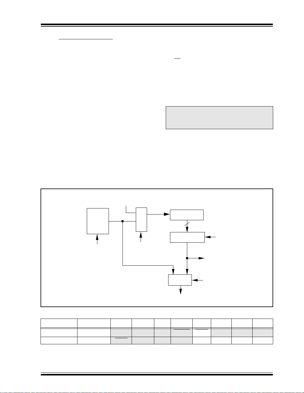
PIC12CE67X
9.7 Watchdog Timer (WDT)
The Watchdog Timer is a free running on-chip RC oscillator which does not require any external components.
This RC oscillator is separate from the RC oscillator of
the OSC1/CLKIN pin. That means that the WDT will
run, even if the clock on the OSC1/CLKIN and OSC2/
CLKOUT pins of the device has been stopped, for
example, by execution of a SLEEP instruction. During
normal operation, a WDT time-out generates a device
RESET (Watchdog Timer Reset). If the device is in
SLEEP mode, a WDT time-out causes the device to
wake-up and continue with normal operation (Watchdog Timer Wake-up). The WDT can be permanently
disabled by clearing configuration bit WDTE
(Section 9.1).
9.7.1 WDT PERIOD The WDT has a nominal time-out period of 18 ms, (with
no prescaler). The time-out periods vary with tempera-
DD
ture, V
and process variations from part to part (see
DC specs). If longer time-out periods are desired, a
prescaler with a division ratio of up to 1:128 can be
assigned to the WDT under software control by writing
to the OPTION register. Thus, time-out periods up to
2.3 seconds can be realized.
FIGURE 9-16: WATCHDOG TIMER BLOCK DIAGRAM
From TMR0 Clock Source
(Figure 7-5)
0
M
1
WDT Timer
U
X
The CLRWDT and SLEEP instructions clear the WDT and
the postscaler, if assigned to the WDT, and prevent it
from timing out early and generating a premature
device RESET condition.
The T
O bit in the STATUS register will be cleared upon
a Watchdog Timer time-out.
9.7.2 WDT PROGRAMMING CONSIDERATIONS It should also be taken into account that under worst
case conditions (V
DD = Min., Temperature = Max., and
max. WDT prescaler) it may take several seconds
before a WDT time-out occurs.
Note: When the prescaler is assigned to the
WDT, always execute a CLRWDT instruction
before changing the prescale value, otherwise a WDT reset may occur.
Postscaler
8
WDT
Enable Bit
Note: PSA and PS2:PS0 are bits in the OPTION register.
PSA
8 - to - 1 MUX
0
MUX
WDT
Time-out
1
PS2:PS0
To TMR0 (Figure 7-5)
PSA
FIGURE 9-17: SUMMARY OF WATCHDOG TIMER REGISTERS
Address Name Bit 7 Bit 6 Bit 5 Bit 4 Bit 3 Bit 2 Bit 1 Bit 0
(1)
2007h
Config. bits
81h OPTION
Legend: Shaded cells are not used by the Watchdog Timer.
Note 1: See Figure 9-1 for operation of these bits. Not all CP0 and CP1 bits are shown.
1998 Microchip Technology Inc. Preliminary DS40181A-page 57
MCLRE CP1 CP0 PWRTE WDTE FOSC2 FOSC1 FOSC0
GPPU INTEDG T0CS T0SE PSA PS2 PS1 PS0

PIC12CE67X
9.8 Power-down Mode (SLEEP)
Power-down mode is entered by executing a SLEEP
instruction.
If enabled, the Watchdog Timer will be cleared but
keeps running, the PD
T
O (STATUS<4>) bit is set, and the oscillator driver is
turned off. The I/O ports maintain the status they had,
before the SLEEP instruction was executed (driving
high, low, or hi-impedance).
For lowest current consumption in this mode, place all
I/O pins at either V
cuitry is drawing current from the I/O pin, power-down
the A/D, disable external clocks. Pull all I/O pins, that
are hi-impedance inputs, high or low externally to avoid
switching currents caused by floating inputs. The
T0CKI input if enabled should also be at V
lowest current consumption. The contribution from onchip pull-ups on GPIO should be considered.
The MCLR
(V
9.8.1 WAKE-UP FROM SLEEP The device can wake up from SLEEP through one of
the following events:
1. External reset input on MCLR
2. Watchdog Timer Wake-up (if WDT was
3. GP2/INT interrupt, interrupt GPIO por t change,
External MCLR
other events are considered a continuation of program
execution and cause a "wake-up". The T
in the STATUS register can be used to determine the
cause of device reset. The PD
power-up, is cleared when SLEEP is inv oked. The T
is cleared if a WDT time-out occurred (and caused
wake-up).
The following peripheral interrupt can wake the device
from SLEEP:
1. A/D conversion (when A/D clock source is RC).
pin if enabled must be at a logic high level
IHMC).
enabled).
or some Peripheral Interrupts.
bit (STATUS<3>) is cleared, the
DD, or VSS, ensure no external cir-
DD or VSS for
pin.
Reset will cause a device reset. All
O and PD bits
bit, which is set on
O bit
Other peripherals can not generate interrupts since
during SLEEP, no on-chip Q clocks are present.
When the SLEEP instruction is being executed, the next
instruction (PC + 1) is pre-fetched. For the device to
wake-up through an interrupt event, the corresponding
interrupt enable bit must be set (enabled). Wake-up is
regardless of the state of the GIE bit. If the GIE bit is
clear (disabled), the device continues execution at the
instruction after the SLEEP instruction. If the GIE bit is
set (enabled), the device executes the instruction after
the SLEEP instr uction and then branches to the interrupt address (0004h). In cases where the execution of
the instruction following SLEEP is not desirable, the
user should have a NOP after the SLEEP instruction.
9.8.2 WAKE-UP USING INTERRUPTS When global interrupts are disabled (GIE cleared) and
any interrupt source has both its interrupt enable bit
and interrupt flag bit set, one of the following will occur:
• If the interrupt occurs before the the execution of
a SLEEP instruction, the SLEEP instruction will
complete as a NOP. Theref ore, the WDT and WDT
postscaler will not be cleared, the T
be set and PD
• If the interrupt occurs during or after the execution of a SLEEP instruction, the device will immediately wake up from sleep . The SLEEP instruction
will be completely executed before the wake-up.
Therefore, the WDT and WDT postscaler will be
cleared, the T
be cleared.
Even if the flag bits were checked before executing a
SLEEP instruction, it may be possible for flag bits to
become set before the SLEEP instruction completes. To
determine whether a SLEEP instruction executed, test
the PD
bit. If the PD bit is set, the SLEEP instruction was
executed as a NOP.
To ensure that the WDT is cleared, a CLRWDT instruc-
tion should be executed before a SLEEP instruction.
bits will not be cleared.
O bit will be set and the PD bit will
O bit will not
DS40181A-page 58 Preliminary 1998 Microchip Technology Inc.

PIC12CE67X
FIGURE 9-18: WAKE-UP FROM SLEEP THROUGH INTERRUPT
Q1 Q2 Q3 Q4 Q1 Q2 Q3 Q4 Q1 Q1 Q2 Q3 Q4 Q1 Q2 Q3 Q4 Q1 Q2 Q3 Q4 Q1 Q2 Q3 Q4
OSC1
CLKOUT(4)
GPIO pin
GPIF flag
(INTCON<0>)
GIE bit
(INTCON<7>)
INSTR
UCTION FLOW
PC
Instruction
fetched
Instruction
executed
Note 1: XT, HS or LP oscillator mode assumed.
2: T
3: GIE = '1' assumed. In this case after wake- up, the processor jumps to the interrupt routine. If GIE = '0', execution will continue in-line.
4: CLKOUT is not available in XT, HS or LP osc modes, but shown here for timing reference.
PC PC+1 PC+2
Inst(PC) = SLEEP
Inst(PC - 1)
OST = 1024TOSC (drawing not to scale) This delay will not be there for INTRC and EXTRC osc mode.
Inst(PC + 1)
SLEEP
Processor in
SLEEP
TOST(2)
PC+2
Inst(PC + 2)
Inst(PC + 1)
Interrupt Latency
(Note 2)
PC + 2 0004h 0005h
Inst(0004h)
Dummy cycle
Dummy cycle
Inst(0005h)
Inst(0004h)
9.9 Program Verification/Code Protection
If the code protection bit(s) have not been programmed, the on-chip program memory can be read
out for verification purposes.
Note: Microchip does not recommend code pro-
tecting windowed devices.
9.10 ID Locations
Four memory locations (2000h - 2003h) are designated
as ID locations where the user can store checksum or
other code-identification numbers. These locations are
not accessible during normal execution but are readable and writable during program/verify. It is recommended that only the 4 least significant bits of the ID
location are used.
9.11 In-Circuit Serial Programming
PIC12CE67X microcontrollers can be serially programmed while in the end application circuit. This is
simply done with two lines for clock and data, and three
other lines for power, ground, and the programming
voltage. This allows customers to manufacture boards
with unprogrammed devices, and then program the
microcontroller just before shipping the product. This
also allows the most recent firmware or a custom firmware to be programmed.
The device is placed into a program/verify mode by
holding the GP1 and GP0 pins low while raising the
MCLR
(VPP) pin from VIL to VIHH (see programming
specification). GP1 (clock) becomes the programming
clock and GP0 (data) becomes the programming data.
Both GP0 and GP1 are Schmitt Trigger inputs in this
mode.
After reset, to place the device into programming/verify
mode, the program counter (PC) is at location 00h. A 6bit command is then supplied to the device. Depending
on the command, 14-bits of program data are then supplied to or from the device, depending if the command
was a load or a read. For complete details of serial programming, please refer to the PIC12CE67X Programming Specifications.
FIGURE 9-19: TYPICAL IN-CIRCUIT SERIAL
PROGRAMMING
CONNECTION
To Normal
External
Connector
Signals
+5V
0V
VPP
CLK
Data I/O
Connections
To Normal
Connections
PIC12CE67X
DD
V
VSS
MCLR/VPP
GP1
GP0
VDD
1998 Microchip Technology Inc. Preliminary DS40181A-page 59

PIC12CE67X
NOTES:
DS40181A-page 60 Preliminary 1998 Microchip Technology Inc.

PIC12CE67X
10.0 INSTRUCTION SET SUMMARY
Each PIC12CE67X instruction is a 14-bit word divided
into an OPCODE which specifies the instruction type
and one or more operands which further specify the
operation of the instruction. The PIC12CE67X instruction set summary in Tab le 10-2 lists byte-oriented, bit-
oriented, and literal and control operations. Table 10-
1 shows the opcode field descriptions.
For byte-oriented instructions, 'f' represents a file register designator and 'd' represents a destination designator. The file register designator specifies which file
register is to be used by the instruction.
The destination designator specifies where the result of
the operation is to be placed. If 'd' is zero, the result is
placed in the W register. If 'd' is one, the result is placed
in the file register specified in the instruction.
For bit-oriented instructions, 'b' represents a bit field
designator which selects the number of the bit affected
by the operation, while 'f' represents the number of the
file in which the bit is located.
For literal and control operations, 'k' represents an
eight or eleven bit constant or literal value.
TABLE 10-1: OPCODE FIELD
Field Description
f Register file address (0x00 to 0x7F)
W Working register (accumulator)
b Bit address within an 8-bit file register
k Literal field, constant data or label
x Don't care location (= 0 or 1)
The assembler will generate code with x = 0. It is the
recommended form of use for compatibility with all
Microchip software tools.
d Destination select; d = 0: store result in W,
d = 1: store result in file register f.
Default is d = 1
label Label name
TOS Top of Stack
PC Program Counter
PCLATH
Program Counter High Latch
GIE Global Interrupt Enable bit
WDT Watchdog Timer/Counter
TO Time-out bit
PD Power-down bit
dest Destination either the W register or the specified
register file location
[ ] Options
Contents
( )
Assigned to
→
Register bit field
< >
In the set of
∈
User defined term (font is courier)
i
talics
DESCRIPTIONS
The instruction set is highly orthogonal and is grouped
into three basic categories:
• Byte-oriented operations
• Bit-oriented operations
• Literal and control operations
All instructions are executed within one single instruc-
tion cycle, unless a conditional test is true or the program counter is changed as a result of an instruction.
In this case, the execution takes two instruction cycles
with the second cycle executed as a NOP. One instruction cycle consists of four oscillator periods. Thus, for
an oscillator frequency of 4 MHz, the normal instruction
execution time is 1 µs. If a conditional test is true or the
program counter is changed as a result of an instruction, the instruction execution time is 2 µs.
Table 10-2 lists the instructions recognized by the
MPASM assembler.
Figure 10-1 shows the three general formats that the
instructions can have.
Note: To maintain upward compatibility with
future PIC12CE67X products, do not use
the OPTION and TRIS instructions.
All examples use the following format to represent a
hexadecimal number:
0xhh
where h signifies a hexadecimal digit.
FIGURE 10-1: GENERAL FORMAT FOR
INSTRUCTIONS
Byte-oriented file register operations
13 8 7 6 0
OPCODE d f (FILE #)
d = 0 for destination W
d = 1 for destination f
f = 7-bit file register address
Bit-oriented file register operations
13 10 9 7 6 0
OPCODE b (BIT #) f (FILE #)
b = 3-bit bit address
f = 7-bit file register address
Literal and control operations
General
13 8 7 0
OPCODE k (literal)
k = 8-bit immediate value
CALL and GOTO instructions only
13 11 10 0
OPCODE k (literal)
k = 11-bit immediate value
1998 Microchip Technology Inc. Preliminary DS40181A-page 61

PIC12CE67X
10.1 Special Function Registers as
Source/Destination
The PIC12CE67X’s orthogonal instruction set allows
read and write of all file registers, including special
function registers. There are some special situations
the user should be aware of:
10.1.1 STATUS AS DESTINATION
If an instruction writes to STATUS , the Z, C and DC bits
may be set or cleared as a result of the instruction and
overwrite the original data bits written. For example,
executing CLRF STATUS will clear register ST ATUS, and
then set the Z bit leaving 0000 0100b in the register.
10.1.2 TRIS AS DESTINATION
Bit 3 of the TRIS register always reads as a '1' since
GP3 is an input only pin. This fact can aff ect some readmodify-write operations on the TRIS register.
10.1.3 PCL AS SOURCE OR DESTINATION Read, write or read-modify-write on PCL may have the
following results:
Read PC: PCL → dest
Write PCL: PCLATH → PCH;
8-bit destination value → PCL
Read-Modify-Write: PCL→ ALU operand
PCLATH → PCH;
8-bit result → PCL
Where PCH = program counter high byte (not an
addressable register), PCLATH = Program counter
high holding latch, dest = destination, WREG or f.
10.1.4 BIT MANIPULATION All bit manipulation instructions are done by first read-
ing the entire register, operating on the selected bit and
writing the result back (read-modify-write). The user
should keep this in mind when operating on special
function registers, such as ports.
DS40181A-page 62 Preliminary 1998 Microchip Technology Inc.

PIC12CE67X
TABLE 10-2: INSTRUCTION SET SUMMARY
Mnemonic,
Operands
BYTE-ORIENTED FILE REGISTER OPERATIONS
ADDWF
ANDWF
CLRF
CLRW
COMF
DECF
DECFSZ
INCF
INCFSZ
IORWF
MOVF
MOVWF
NOP
RLF
RRF
SUBWF
SWAPF
XORWF
BIT-ORIENTED FILE REGISTER OPERATIONS
BCF
BSF
BTFSC
BTFSS
LITERAL AND CONTROL OPERATIONS
ADDLW
ANDLW
CALL
CLRWDT
GOTO
IORLW
MOVLW
RETFIE
RETLW
RETURN
SLEEP
SUBLW
XORLW
Note 1: When an I/O register is modified as a function of itself ( e.g., MOVF PORTB, 1), the value used will be that value present
on the pins themselves. For example, if the data latch is '1' for a pin configured as input and is driven low by an external
device, the data will be written back with a '0'.
2: If this instruction is executed on the TMR0 register (and, where applicab le , d = 1), the prescaler will be cleared if assigned
to the Timer0 Module.
3: If Program Counter (PC) is modified or a conditional test is true, the instruction requires two cycles. The second cycle is
executed as a NOP.
Description Cycles 14-Bit Opcode Status
MSb LSb
f, d
Add W and f
f, d
AND W with f
f
Clear f
-
Clear W
f, d
Complement f
f, d
Decrement f
f, d
Decrement f, Skip if 0
f, d
Increment f
f, d
Increment f, Skip if 0
f, d
Inclusive OR W with f
f, d
Move f
f
Move W to f
-
No Operation
f, d
Rotate Left f through Carry
f, d
Rotate Right f through Carry
f, d
Subtract W from f
f, d
Swap nibbles in f
f, d
Exclusive OR W with f
f, b
Bit Clear f
f, b
Bit Set f
f, b
Bit Test f, Skip if Clear
f, b
Bit Test f, Skip if Set
k
Add literal and W
k
AND literal with W
k
Call subroutine
-
Clear Watchdog Timer
k
Go to address
k
Inclusive OR literal with W
k
Move literal to W
-
Return from interrupt
k
Return with literal in W
-
Return from Subroutine
-
Go into standby mode
k
Subtract W from literal
k
Exclusive OR literal with W
1
1
1
1
1
1
1(2)
1
1(2)
1
1
1
1
1
1
1
1
1
1
1
1 (2)
1 (2)
1
1
2
1
2
1
1
2
2
2
1
1
1
00
0111
0101
0001
0001
1001
0011
1011
1010
1111
0100
1000
0000
0000
1101
1100
0010
1110
0110
00bb
01bb
10bb
11bb
111x
1001
0kkk
0000
1kkk
1000
00xx
0000
01xx
0000
0000
110x
1010
dfff
dfff
lfff
0xxx
dfff
dfff
dfff
dfff
dfff
dfff
dfff
lfff
0xx0
dfff
dfff
dfff
dfff
dfff
bfff
bfff
bfff
bfff
kkkk
kkkk
kkkk
0110
kkkk
kkkk
kkkk
0000
kkkk
0000
0110
kkkk
kkkk
00
00
00
00
00
00
00
00
00
00
00
00
00
00
00
00
00
01
01
01
01
11
11
10
00
10
11
11
00
11
00
00
11
11
ffff
ffff
ffff
xxxx
ffff
ffff
ffff
ffff
ffff
ffff
ffff
ffff
0000
ffff
ffff
ffff
ffff
ffff
ffff
ffff
ffff
ffff
kkkk
kkkk
kkkk
0100
kkkk
kkkk
kkkk
1001
kkkk
1000
0011
kkkk
kkkk
Affected
C,DC,Z
Z
Z
Z
Z
Z
Z
Z
Z
C
C
C,DC,Z
Z
C,DC,Z
Z
O,PD
T
Z
TO,PD
C,DC,Z
Z
Notes
1,2
1,2
2
1,2
1,2
1,2,3
1,2
1,2,3
1,2
1,2
1,2
1,2
1,2
1,2
1,2
1,2
1,2
3
3
1998 Microchip Technology Inc. Preliminary DS40181A-page 63

PIC12CE67X
10.2 Instruction Descriptions
ADDLW Add Literal and W
label
Syntax: [
] ADDLW k
Operands: 0 ≤ k ≤ 255
Operation: (W) + k → (W)
Status Affected: C, DC, Z
Encoding:
Description:
11 111x kkkk kkkk
The contents of the W register are
added to the eight bit literal 'k' and the
result is placed in the W register
Words: 1
Cycles: 1
Example
ADDLW 0x15
Before Instruction
W = 0x10
After Instruction
W = 0x25
ADDWF Add W and f
label
Syntax: [
] ADDWF f,d
Operands: 0 ≤ f ≤ 127
d ∈ [0,1]
Operation: (W) + (f) → (dest)
Status Affected: C, DC, Z
Encoding:
Description:
00 0111 dfff ffff
Add the contents of the W register
with register 'f'. If 'd' is 0 the result is
stored in the W register. If 'd' is 1 the
result is stored back in register 'f'
Words: 1
Cycles: 1
Example
ADDWF FSR, 0
Before Instruction
W = 0x17
FSR = 0xC2
After Instruction
W = 0xD9
FSR = 0xC2
ANDLW And Literal with W
label
Syntax: [
] ANDLW k
Operands: 0 ≤ k ≤ 255
Operation: (W) .AND. (k) → (W)
Status Affected: Z
Encoding:
Description:
.
11 1001 kkkk kkkk
The contents of W register are
AND’ed with the eight bit literal 'k'. The
result is placed in the W register
.
Words: 1
Cycles: 1
Example
ANDLW 0x5F
Before Instruction
W = 0xA3
After Instruction
W = 0x03
ANDWF AND W with f
label
Syntax: [
] ANDWF f,d
Operands: 0 ≤ f ≤ 127
d ∈ [0,1]
Operation: (W) .AND. (f) → (dest)
Status Affected: Z
Encoding:
Description:
.
00 0101 dfff ffff
AND the W register with register 'f'. If
'd' is 0 the result is stored in the W
register. If 'd' is 1 the result is stored
back in register 'f'
.
Words: 1
Cycles: 1
Example
ANDWF FSR, 1
Before Instruction
W = 0x17
FSR = 0xC2
After Instruction
W = 0x17
FSR = 0x02
DS40181A-page 64 Preliminary 1998 Microchip Technology Inc.

PIC12CE67X
BCF Bit Clear f
label
Syntax: [
] BCF f,b
Operands: 0 ≤ f ≤ 127
0 ≤ b ≤ 7
Operation: 0 → (f<b>)
Status Affected: None
Encoding:
01 00bb bfff ffff
Description: Bit 'b' in register 'f' is cleared.
Words: 1
Cycles: 1
Example
BCF FLAG_REG, 7
Before Instruction
After Instruction
FLAG_REG = 0xC7
FLAG_REG = 0x47
BSF Bit Set f
label
Syntax: [
] BSF f,b
Operands: 0 ≤ f ≤ 127
0 ≤ b ≤ 7
Operation: 1 → (f<b>)
Status Affected: None
Encoding:
Description:
01 01bb bfff ffff
Bit 'b' in register 'f' is set.
Words: 1
Cycles: 1
Example
BSF FLAG_REG, 7
Before Instruction
After Instruction
FLAG_REG = 0x0A
FLAG_REG = 0x8A
BTFSC Bit Test, Skip if Clear
label
Syntax: [
] BTFSC f,b
Operands: 0 ≤ f ≤ 127
0 ≤ b ≤ 7
Operation: skip if (f<b>) = 0
Status Affected: None
Encoding:
Description:
01 10bb bfff ffff
If bit 'b' in register 'f' is '0' then the next
instruction is skipped.
If bit 'b' is '0' then the next instruction
fetched during the current instruction
execution is discarded, and a NOP is
executed instead, making this a 2 cycle
instruction
.
Words: 1
Cycles: 1(2)
Example
HERE
FALSE
TRUE
BTFSC
GOTO
•
•
•
FLAG,1
PROCESS_CODE
Before Instruction
PC = address HERE
After Instruction
if FLAG<1> = 0,
PC = address TRUE
if FLAG<1>=1,
PC = address FALSE
1998 Microchip Technology Inc. Preliminary DS40181A-page 65

PIC12CE67X
BTFSS Bit Test f, Skip if Set
label
Syntax: [
] BTFSS f,b
Operands: 0 ≤ f ≤ 127
0 ≤ b < 7
Operation: skip if (f<b>) = 1
Status Affected: None
Encoding:
Description:
01 11bb bfff ffff
If bit 'b' in register 'f' is '1' then the next
instruction is skipped.
If bit 'b' is '1', then the next instruction
fetched during the current instruction
execution, is discarded and a NOP is
executed instead, making this a 2 cycle
instruction.
Words: 1
Cycles: 1(2)
Example
HERE
FALSE
TRUE
BTFSS
GOTO
•
•
•
FLAG,1
PROCESS_CODE
Before Instruction
PC = address HERE
After Instruction
if FLAG<1> = 0,
PC = address FALSE
if FLAG<1> = 1,
PC = address TRUE
CALL Call Subroutine
label
Syntax: [
] CALL k
Operands: 0 ≤ k ≤ 2047
Operation: (PC)+ 1→ TOS,
k → PC<10:0>,
(PCLATH<4:3>) → PC<12:11>
Status Affected: None
Encoding:
Description:
10 0kkk kkkk kkkk
Call Subroutine. First, return address
(PC+1) is pushed onto the stack. The
eleven bit immediate address is loaded
into PC bits <10:0>. The upper bits of
the PC are loaded from PCLATH.
CALL is a two cycle instruction.
Words: 1
Cycles: 2
Example
HERE CALL THERE
Before Instruction
PC = Address HERE
After Instruction
PC = Address THERE
TOS= Address HERE+1
CLRF Clear f
label
Syntax: [
] CLRF f
Operands: 0 ≤ f ≤ 127
Operation: 00h → (f)
1 → Z
Status Affected: Z
Encoding:
Description:
00 0001 1fff ffff
The contents of register 'f' are cleared
and the Z bit is set.
Words: 1
Cycles: 1
Example
CLRF FLAG_REG
Before Instruction
After Instruction
CLRW Clear W
label
Syntax: [
] CLRW
Operands: None
Operation: 00h → (W)
1 → Z
Status Affected: Z
Encoding:
Description:
00 0001 0xxx xxxx
W register is cleared. Zero bit (Z) is
set.
Words: 1
Cycles: 1
Example
CLRW
Before Instruction
After Instruction
FLAG_REG = 0x5A
FLAG_REG = 0x00
Z = 1
W = 0x5A
W = 0x00
Z = 1
DS40181A-page 66 Preliminary 1998 Microchip Technology Inc.

PIC12CE67X
CLRWDT Clear Watchdog Timer
label
Syntax: [
] CLRWDT
Operands: None
Operation: 00h → WDT
0 → WDT prescaler,
O
1 → T
1 → PD
Status Affected: TO, PD
Encoding:
Description:
00 0000 0110 0100
CLRWDT instruction resets the Watch-
dog Timer. It also resets the prescaler
of the WDT. Status bits TO and PD
are set.
Words: 1
Cycles: 1
Example
CLRWDT
Before Instruction
After Instruction
WDT counter = ?
WDT counter = 0x00
WDT prescaler= 0
TO = 1
PD = 1
COMF Complement f
label
Syntax: [
] COMF f,d
Operands: 0 ≤ f ≤ 127
d ∈ [0,1]
Operation: (f
) → (dest)
Status Affected: Z
Encoding:
Description:
00 1001 dfff ffff
The contents of register 'f' are complemented. If 'd' is 0 the result is stored in
W. If 'd' is 1 the result is stored back in
register 'f'.
Words: 1
Cycles: 1
Example
COMF REG1,0
Before Instruction
After Instruction
REG1 = 0x13
REG1 = 0x13
W = 0xEC
DECF Decrement f
label
Syntax: [
] DECF f,d
Operands: 0 ≤ f ≤ 127
d ∈ [0,1]
Operation: (f) - 1 → (dest)
Status Affected: Z
Encoding:
Description:
00 0011 dfff ffff
Decrement register 'f'. If 'd' is 0 the
result is stored in the W register. If 'd'
is 1 the result is stored back in register
'f'
.
Words: 1
Cycles: 1
Example
DECF CNT, 1
Before Instruction
CNT = 0x01
Z = 0
After Instruction
CNT = 0x00
Z = 1
DECFSZ Decrement f, Skip if 0
label
Syntax: [
] DECFSZ f,d
Operands: 0 ≤ f ≤ 127
d ∈ [0,1]
Operation: (f) - 1 → (dest); skip if result = 0
Status Affected: None
Encoding:
Description:
00 1011 dfff ffff
The contents of register 'f' are decre-
mented. If 'd' is 0 the result is placed in
the W register. If 'd' is 1 the result is
placed back in register 'f'.
If the result is 0, the next instruction,
which is already fetched, is discarded. A
NOP is executed instead making it a two
cycle instruction.
Words: 1
Cycles: 1(2)
Example
HERE DECFSZ CNT, 1
GOTO LOOP
CONTINUE •
•
•
Before Instruction
PC = address HERE
After Instruction
CNT = CNT - 1
if CNT = 0,
PC = address CONTINUE
if CNT ≠ 0,
PC = address HERE+1
1998 Microchip Technology Inc. Preliminary DS40181A-page 67

PIC12CE67X
GOTO Unconditional Branch
label
Syntax: [
] GOTO k
Operands: 0 ≤ k ≤ 2047
Operation: k → PC<10:0>
PCLATH<4:3> → PC<12:11>
Status Affected: None
Encoding:
Description:
10 1kkk kkkk kkkk
GOTO is an unconditional branch. The
eleven bit immediate value is loaded
into PC bits <10:0>. The upper bits of
PC are loaded from PCLATH<4:3>.
GOTO is a two cycle instruction.
Words: 1
Cycles: 2
Example
GOTO THERE
After Instruction
PC = Address THERE
INCFSZ Increment f, Skip if 0
label
Syntax: [
] INCFSZ f,d
Operands: 0 ≤ f ≤ 127
d ∈ [0,1]
Operation: (f) + 1 → (dest), skip if result = 0
Status Affected: None
Encoding:
Description:
00 1111 dfff ffff
The contents of register 'f' are incre-
mented. If 'd' is 0 the result is placed
in the W register. If 'd' is 1 the result is
placed back in register 'f'.
If the result is 0, the next instruction,
which is already fetched, is discarded.
A NOP is executed instead making it a
two cycle instruction
.
Words: 1
Cycles: 1(2)
Example
HERE INCFSZ CNT, 1
GOTO LOOP
CONTINUE •
•
•
Before Instruction
PC = address HERE
After Instruction
CNT = CNT + 1
if CNT= 0,
PC = address CONTINUE
if CNT≠ 0,
PC = address HERE +1
INCF Increment f
label
Syntax: [
] INCF f,d
Operands: 0 ≤ f ≤ 127
d ∈ [0,1]
Operation: (f) + 1 → (dest)
Status Affected: Z
Encoding:
Description:
00 1010 dfff ffff
The contents of register 'f' are incre-
mented. If 'd' is 0 the result is placed
in the W register. If 'd' is 1 the result is
placed back in register 'f'.
Words: 1
Cycles: 1
Example
INCF CNT, 1
Before Instruction
CNT = 0xFF
Z = 0
After Instruction
CNT = 0x00
Z = 1
DS40181A-page 68 Preliminary 1998 Microchip Technology Inc.
IORLW Inclusive OR Literal with W
label
Syntax: [
] IORLW k
Operands: 0 ≤ k ≤ 255
Operation: (W) .OR. k → (W)
Status Affected: Z
Encoding:
Description:
11 1000 kkkk kkkk
The contents of the W register is
OR’ed with the eight bit literal 'k'. The
result is placed in the W register
Words: 1
Cycles: 1
Example
IORLW 0x35
Before Instruction
W = 0x9A
After Instruction
W = 0xBF
Z = 1
.

PIC12CE67X
IORWF Inclusive OR W with f
label
Syntax: [
] IORWF f,d
Operands: 0 ≤ f ≤ 127
d ∈ [0,1]
Operation: (W) .OR. (f) → (dest)
Status Affected: Z
Encoding:
Description:
00 0100 dfff ffff
Inclusive OR the W register with regis-
ter 'f'. If 'd' is 0 the result is placed in
the W register. If 'd' is 1 the result is
placed back in register 'f'.
Words: 1
Cycles: 1
Example
IORWF RESULT, 0
Before Instruction
RESULT = 0x13
W = 0x91
After Instruction
RESULT = 0x13
W = 0x93
Z = 1
MOVLW Move Literal to W
label
Syntax: [
] MOVLW k
Operands: 0 ≤ k ≤ 255
Operation: k → (W)
Status Affected: None
Encoding:
Description:
11 00xx kkkk kkkk
The eight bit literal 'k' is loaded into W
register
. The don’t cares will assemble
as 0’s.
Words: 1
Cycles: 1
Example
MOVLW 0x5A
After Instruction
W = 0x5A
MOVF Move f
label
Syntax: [
] MOVF f,d
Operands: 0 ≤ f ≤ 127
d ∈ [0,1]
Operation: (f) → (dest)
Status Affected: Z
Encoding:
Description:
00 1000 dfff ffff
The contents of register f is moved to
a destination dependant upon the sta-
tus of d. If d = 0, destination is W reg-
ister. If d = 1, the destination is file
register f itself. d = 1 is useful to test a
file register since status flag Z is
affected.
Words: 1
Cycles: 1
Example
MOVF FSR, 0
After Instruction
W = value in FSR register
Z = 1
MOVWF Move W to f
label
Syntax: [
] MOVWF f
Operands: 0 ≤ f ≤ 127
Operation: (W) → (f)
Status Affected: None
Encoding:
Description:
00 0000 1fff ffff
Move data from W register to register
'f'
.
Words: 1
Cycles: 1
Example
MOVWF OPTION
Before Instruction
OPTION = 0xFF
W = 0x4F
After Instruction
OPTION = 0x4F
W = 0x4F
1998 Microchip Technology Inc. Preliminary DS40181A-page 69
PIC12CE67X
NOP No Operation
label
Syntax: [
] NOP
Operands: None
Operation: No operation
Status Affected: None
Encoding:
Description:
00 0000 0xx0 0000
No operation.
Words: 1
Cycles: 1
Example
NOP
OPTION Load Option Register
Syntax: [
label
] OPTION
Operands: None
Operation: (W) → OPTION
Status Affected: None
Encoding:
Description:
00 0000 0110 0010
The contents of the W register are
loaded in the OPTION register. This
instruction is supported for code compatibility with PIC16C5X products.
Since OPTION is a readable/writable
register, the user can directly address
it.
Words: 1
Cycles: 1
Example
To maintain upward compatibility
with future PIC12C67X products,
do not use this instruction.
RETFIE Return from Interrupt
label
Syntax: [
] RETFIE
Operands: None
Operation: TOS → PC,
1 → GIE
Status Affected: None
Encoding:
Description:
00 0000 0000 1001
Return from Interrupt. Stack is POPed
and Top of Stack (TOS) is loaded in
the PC. Interrupts are enabled by set-
ting Global Interrupt Enable bit, GIE
(INTCON<7>). This is a two cycle
instruction.
Words: 1
Cycles: 2
Example
RETFIE
After Interrupt
PC = TOS
GIE = 1
RETLW Return with Literal in W
label
Syntax: [
] RETLW k
Operands: 0 ≤ k ≤ 255
Operation: k → (W);
TOS → PC
Status Affected: None
Encoding:
Description:
11 01xx kkkk kkkk
The W register is loaded with the eight
bit literal 'k'. The program counter is
loaded from the top of the stack (the
return address). This is a two cycle
instruction.
Words: 1
Cycles: 2
Example
CALL TABLE ;W contains table
;offset value
• ;W now has table value
•
•
TABLE
ADDWF PC ;W = offset
RETLW k1 ;Begin table
RETLW k2 ;
•
•
•
RETLW kn ; End of table
Before Instruction
W = 0x07
After Instruction
W = value of k8
DS40181A-page 70 Preliminary 1998 Microchip Technology Inc.

PIC12CE67X
Register fC
RETURN Return from Subroutine
label
Syntax: [
] RETURN
Operands: None
Operation: TOS → PC
Status Affected: None
Encoding:
Description:
00 0000 0000 1000
Return from subroutine. The stack is
POPed and the top of the stack (T OS)
is loaded into the program counter.
This is a two cycle instruction.
Words: 1
Cycles: 2
Example
RETURN
After Interrupt
PC = TOS
RLF Rotate Left f through Carry
label
Syntax: [
] RLF f,d
Operands: 0 ≤ f ≤ 127
d ∈ [0,1]
Operation: See description below
Status Affected: C
Encoding:
Description:
00 1101 dfff ffff
The contents of register 'f' are rotated
one bit to the left through the Carry
Flag. If 'd' is 0 the result is placed in
the W register. If 'd' is 1 the result is
stored back in register 'f'.
Register fC
Words: 1
Cycles: 1
Example
RLF REG1,0
Before Instruction
REG1 = 1110 0110
C = 0
After Instruction
REG1 = 1110 0110
W = 1100 1100
C = 1
RRF Rotate Right f through Carry
label
Syntax: [
] RRF f,d
Operands: 0 ≤ f ≤ 127
d ∈ [0,1]
Operation: See description below
Status Affected: C
Encoding:
Description:
00 1100 dfff ffff
The contents of register 'f' are rotated
one bit to the right through the Carry
Flag. If 'd' is 0 the result is placed in
the W register. If 'd' is 1 the result is
placed back in register 'f'.
Words: 1
Cycles: 1
Example
RRF REG1,0
Before Instruction
REG1 = 1110 0110
C = 0
After Instruction
REG1 = 1110 0110
W = 0111 0011
C = 0
SLEEP
Syntax: [
label
] SLEEP
Operands: None
Operation: 00h → WDT,
0 → WDT prescaler,
O,
1 → T
0 → PD
Status Affected: TO, PD
Encoding:
Description:
00 0000 0110 0011
The power-down status bit, PD is
cleared. Time-out status bit, TO is
set. Watchdog Timer and its pres-
caler are cleared.
The processor is put into SLEEP
mode with the oscillator stopped.
Words: 1
Cycles: 1
Example: SLEEP
1998 Microchip Technology Inc. Preliminary DS40181A-page 71

PIC12CE67X
SUBLW Subtract W from Literal
label
Syntax: [
] SUBLW k
Operands: 0 ≤ k ≤ 255
Operation: k - (W) → (W)
Status
C, DC, Z
Affected:
Encoding: 11 110x kkkk kkkk
Description:
The W register is subtracted (2’s complement method) from the eight bit literal
'k'. The result is placed in the W register.
Words: 1
Cycles: 1
Example 1: SUBLW 0x02
Before Instruction
W = 1
C = ?
After Instruction
W = 1
C = 1; result is positive
Example 2: Before Instruction
W = 2
C = ?
After Instruction
W = 0
C = 1; result is zero
Example 3: Before Instruction
W = 3
C = ?
After Instruction
W = 0xFF
C = 0; result is negative
SUBWF Subtract W from f
label
Syntax: [
] SUBWF f,d
Operands: 0 ≤ f ≤ 127
d ∈ [0,1]
Operation: (f) - (W) → (dest)
Status
C, DC, Z
Affected:
Encoding: 00 0010 dfff ffff
Description:
Subtract (2’s complement method) W reg-
ister from register 'f'. If 'd' is 0 the result is
stored in the W register. If 'd' is 1 the
result is stored back in register 'f'.
Words: 1
Cycles: 1
Example 1: SUBWF REG1,1
Before Instruction
REG1 = 3
W = 2
C = ?
After Instruction
REG1 = 1
W = 2
C = 1; result is positive
Example 2: Before Instruction
REG1 = 2
W = 2
C = ?
After Instruction
REG1 = 0
W = 2
C = 1; result is zero
Example 3: Before Instruction
REG1 = 1
W = 2
C = ?
After Instruction
REG1 = 0xFF
W = 2
C = 0; result is negative
DS40181A-page 72 Preliminary 1998 Microchip Technology Inc.

PIC12CE67X
SWAPF Swap Nibbles in f
label
Syntax: [
] SWAPF f,d
Operands: 0 ≤ f ≤ 127
d ∈ [0,1]
Operation: (f<3:0>) → (dest<7:4>),
(f<7:4>) → (dest<3:0>)
Status Affected: None
00
Encoding:
Description:
The upper and lower nibbles of register 'f' are exchanged. If 'd' is 0 the
result is placed in W register. If 'd' is 1
the result is placed in register 'f'.
1110 dfff ffff
Words: 1
Cycles: 1
Example
SWAPF REG, 0
Before Instruction
REG1 = 0xA5
After Instruction
REG1 = 0xA5
W = 0x5A
TRIS Load TRIS Register
Syntax: [
label
] TRIS f
Operands: 5 ≤ f ≤ 7
Operation: (W) → TRIS register f;
Status Affected: None
Encoding:
Description:
00
0000 0110 0fff
The instruction is supported for code
compatibility with the PIC16C5X products. Since TRIS registers are readable and writable, the user can directly
address them.
Words: 1
Cycles: 1
Example
To maintain upward compatibility
with future PIC12C67X products,
do not use this instruction.
XORLW Exclusive OR Literal with W
Syntax: [
label
] XORLW k
Operands: 0 ≤ k ≤ 255
Operation: (W) .XOR. k → (W)
Status Affected: Z
Encoding: 11 1010 kkkk kkkk
Description:
The contents of the W register are
XOR’ed with the eight bit literal 'k'.
The result is placed in the W register.
Words: 1
Cycles: 1
Example: XORLW 0xAF
Before Instruction
W = 0xB5
After Instruction
W = 0x1A
XORWF Exclusive OR W with f
label
Syntax: [
] XORWF f,d
Operands: 0 ≤ f ≤ 127
d ∈ [0,1]
Operation: (W) .XOR. (f) → (dest)
Status Affected: Z
Encoding:
Description:
00 0110 dfff ffff
Exclusive OR the contents of the W
register with register 'f'. If 'd' is 0 the
result is stored in the W register. If 'd'
is 1 the result is stored back in register
'f'.
Words: 1
Cycles: 1
Example XORWF
REG 1
Before Instruction
REG = 0xAF
W = 0xB5
After Instruction
REG = 0x1A
W = 0xB5
1998 Microchip Technology Inc. Preliminary DS40181A-page 73

PIC12CE67X
NOTES:
DS40181A-page 74 Preliminary 1998 Microchip Technology Inc.

PIC12CE67X
11.0 DEVELOPMENT SUPPORT
11.1 Development Tools
The PICmicrο microcontrollers are supported with a
full range of hardware and software dev elopment tools:
• PICMASTER
In-Circuit Emulator
• ICEPIC Low-Cost PIC16C5X and PIC16CXXX
In-Circuit Emulator
• PRO MATE
• PICSTART
Programmer
• PICDEM-1 Low-Cost Demonstration Board
• PICDEM-2 Low-Cost Demonstration Board
• PICDEM-3 Low-Cost Demonstration Board
• MPASM Assembler
• MPLAB SIM Software Simulator
• MPLAB-C17 (C Compiler)
• Fuzzy Logic Development System
(
fuzzy
11.2 PICMASTER: High Performance
The PICMASTER Universal In-Circuit Emulator is
intended to provide the product development engineer
with a complete microcontroller design tool set for all
microcontrollers in the PIC14C000, PIC12CXXX,
PIC16C5X, PIC16CXXX and PIC17CXX families.
PICMASTER is supplied with the MPLAB Integrated
Development Environment (IDE), which allows editing,
“make” and download, and source debugging from a
single environment.
Interchangeable target probes allow the system to be
easily reconfigured for emulation of different processors. The universal architecture of the PICMASTER
allows expansion to support all new Microchip microcontrollers.
The PICMASTER Emulator System has been
designed as a real-time emulation system with
advanced features that are generally found on more
expensive development tools. The PC compatible 386
(and higher) machine platform and Microsoft Windows
3.x environment were chosen to best make these fea-
tures available to you, the end user.
A CE compliant version of PICMASTER is availab le f or
European Union (EU) countries.
/PICMASTER CE Real-Time
II Universal Programmer
Plus Entry-Level Prototype
TECH−MP)
Universal In-Circuit Emulator with
MPLAB IDE
11.3 ICEPIC: Low-Cost PICmicro™
In-Circuit Emulator
ICEPIC is a low-cost in-circuit emulator solution for the
Microchip PIC12CXXX, PIC16C5X and PIC16CXXX
families of 8-bit OTP microcontrollers.
ICEPIC is designed to operate on PC-compatible
machines ranging from 286-AT
based machines under Windows 3.x environment.
ICEPIC features real time, non-intrusive emulation.
through Pentium
11.4 PRO MATE II: Universal Programmer
The PRO MATE II Universal Programmer is a full-featured programmer capable of operating in stand-alone
mode as well as PC-hosted mode. PRO MATE II is CE
compliant.
The PRO MATE II has programmable V
supplies which allows it to verify programmed memory
at V
DD min and VDD max for maximum reliability. It has
an LCD display for displaying error messages, keys to
enter commands and a modular detachable socket
assembly to support various package types. In standalone mode the PRO MATE II can read, verify or program PIC12CXXX, PIC14C000, PIC16C5X,
PIC16CXXX and PIC17CXX devices. It can also set
configuration and code-protect bits in this mode.
DD and VPP
11.5 PICSTART Plus Entry Level
Development System
The PICSTART programmer is an easy-to-use, lowcost prototype programmer. It connects to the PC via
one of the COM (RS-232) ports. MPLAB Integrated
Development Environment software makes using the
programmer simple and efficient. PICSTART Plus is
not recommended for production programming.
PICSTART Plus supports all PIC12CXXX, PIC14C000,
PIC16C5X, PIC16CXXX and PIC17CXX devices with
up to 40 pins. Larger pin count devices such as the
PIC16C923, PIC16C924 and PIC17C756 may be supported with an adapter socket. PICSTART Plus is CE
compliant.
1998 Microchip Technology Inc. DS40181A - page 75

PIC12CE67X
11.6 PICDEM-1 Low-Cost PICmicro
Demonstration Board
The PICDEM-1 is a simple board which demonstrates
the capabilities of several of Microchip’s microcontrollers. The microcontrollers supported are: PIC16C5X
(PIC16C54 to PIC16C58A), PIC16C61, PIC16C62X,
PIC16C71, PIC16C8X, PIC17C42, PIC17C43 and
PIC17C44. All necessary hardware and software is
included to run basic demo programs. The users can
program the sample microcontrollers provided with
the PICDEM-1 board, on a PRO MATE II or
PICSTART-Plus programmer, and easily test firmware. The user can also connect the PICDEM-1
board to the PICMASTER emulator and download
the firmware to the emulator for testing. Additional prototype area is available f or the user to b uild some additional hardware and connect it to the microcontroller
socket(s). Some of the features include an RS-232
interface, a potentiometer for simulated analog input,
push-button switches and eight LEDs connected to
PORTB.
11.7 PICDEM-2 Low-Cost PIC16CXX
Demonstration Board
The PICDEM-2 is a simple demonstration board that
supports the PIC16C62, PIC16C64, PIC16C65,
PIC16C73 and PIC16C74 microcontrollers. All the
necessary hardware and software is included to
run the basic demonstration programs. The user
can program the sample microcontrollers provided
with the PICDEM-2 board, on a PRO MATE II programmer or PICSTART-Plus, and easily test firmware.
The PICMASTER emulator may also be used with the
PICDEM-2 board to test firmware. Additional prototype
area has been provided to the user for adding additional hardware and connecting it to the microcontroller
socket(s). Some of the f eatures include a RS-232 interface, push-button switches, a potentiometer for simulated analog input, a Serial EEPROM to demonstrate
usage of the I
tion to an LCD module and a keypad.
2
C bus and separate headers for connec-
11.8 PICDEM-3 Low-Cost PIC16CXXX
Demonstration Board
The PICDEM-3 is a simple demonstration board that
supports the PIC16C923 and PIC16C924 in the PLCC
package. It will also support future 44-pin PLCC
microcontrollers with a LCD Module. All the necessary hardware and software is included to run the
basic demonstration programs. The user can program the sample microcontrollers provided with
the PICDEM-3 board, on a PRO MATE II programmer or PICSTART Plus with an adapter socket, and
easily test firmware. The PICMASTER emulator may
also be used with the PICDEM-3 board to test firmware. Additional prototype area has been provided to
the user for adding hardware and connecting it to the
microcontroller socket(s). Some of the features include
an RS-232 interface, push-button switches, a potentiometer for simulated analog input, a thermistor and
separate headers for connection to an external LCD
module and a keypad. Also pro vided on the PICDEM-3
board is an LCD panel, with 4 commons and 12 segments, that is capable of displaying time, temperature
and day of the week. The PICDEM-3 provides an additional RS-232 interface and Windows 3.1 software for
showing the demultiplexed LCD signals on a PC . A simple serial interface allows the user to construct a hardware demultiplexer for the LCD signals.
11.9 MPLAB™ Integrated Development
Environment Software
The MPLAB IDE Software brings an ease of software
development previously unseen in the 8-bit microcontroller market. MPLAB is a windows based application
which contains:
• A full featured editor
• Three operating modes
- editor
- emulator
- simulator
• A project manager
• Customizable tool bar and key mapping
• A status bar with project information
• Extensive on-line help
MPLAB allows you to:
• Edit your source files (either assembly or ‘C’)
• One touch assemble (or compile) and download
to PICmicro tools (automatically updates all
project information)
• Debug using:
- source files
- absolute listing file
• Transfer data dynamically via DDE (soon to be
replaced by OLE)
• Run up to four emulators on the same PC
The ability to use MPLAB with Microchip’s simulator
allows a consistent platform and the ability to easily
switch from the low cost simulator to the full featured
emulator with minimal retraining due to development
tools.
11.10 Assembler (MPASM)
The MPASM Universal Macro Assembler is a PChosted symbolic assembler. It supports all microcontroller series including the PIC12C5XX, PIC14000,
PIC16C5X, PIC16CXXX, and PIC17CXX families.
MPASM offers full featured Macro capabilities, conditional assembly , and se veral source and listing f ormats.
It generates various object code formats to support
Microchip's development tools as well as third party
programmers.
MPASM allows full symbolic debugging from
PICMASTER, Microchip’s Universal Emulator System.
DS40181A - page 76 1998 Microchip Technology Inc.

PIC12CE67X
MPASM has the following features to assist in de v eloping software for specific use applications.
• Provides translation of Assembler source code to
object code for all Microchip microcontrollers.
• Macro assembly capability.
• Produces all the files (Object, Listing, Symbol, and
special) required for symbolic debug with
Microchip’s emulator systems.
• Supports Hex (default), Decimal and Octal source
and listing formats.
MPASM provides a rich directive language to support
programming of the PICmicro. Directives are helpful in
making the development of your assemb le source code
shorter and more maintainable.
11.11 Software Simulator (MPLAB-SIM)
The MPLAB-SIM Software Simulator allows code
development in a PC host environment. It allows the
user to simulate the PICmicro series microcontrollers
on an instruction level. On any given instruction, the
user may examine or modify any of the data areas or
provide external stimulus to any of the pins. The input/
output radix can be set by the user and the execution
can be performed in; single step, e x ecute until break, or
in a trace mode.
MPLAB-SIM fully supports symbolic debugging using
MPLAB-C and MPASM. The Software Simulator offers
the low cost flexibility to develop and debug code outside of the laboratory environment making it an excellent multi-project software development tool.
11.12 C Compiler (MPLAB-C17)
The MPLAB-C Code Development System is a
complete ‘C’ compiler and integrated development
environment for Microchip’s PIC17CXXX family of
microcontrollers. The compiler provides powerful integration capabilities and ease of use not found with
other compilers.
For easier source level debugging, the compiler provides symbol information that is compatible with the
MPLAB IDE memory display.
11.13 Fuzzy Logic Development System
(
fuzzy
TECH-MP)
fuzzy
TECH-MP fuzzy logic development tool is available in two versions - a low cost introductory version,
MP Explorer, for designers to gain a comprehensive
working knowledge of fuzzy logic system design; and a
full-featured version,
menting more complex systems.
Both versions include Microchip’s
stration board for hands-on experience with fuzzy logic
systems implementation.
fuzzy
TECH-MP, Edition for imple-
fuzzy
LAB demon-
11.14 MP-DriveWay – Application Code
Generator
MP-DriveWay is an easy-to-use Windows-based Application Code Generator. With MP-DriveWay you can
visually configure all the peripherals in a PICmicro
device and, with a click of the mouse, generate all the
initialization and many functional code modules in C
language. The output is fully compatible with Microchip’s MPLAB-C C compiler. The code produced is
highly modular and allows easy integration of your own
code. MP-DriveWay is intelligent enough to maintain
your code through subsequent code generation.
11.15 SEEVAL Evaluation and
Programming System
The SEEVAL SEEPROM Designer’s Kit supports all
Microchip 2-wire and 3-wire Serial EEPROMs. The kit
includes everything necessary to read, write, erase or
program special features of any Microchip SEEPROM
product including Smart Serials and secure serials.
The Total Endurance Disk is included to aid in tradeoff analysis and reliability calculations. The total kit can
significantly reduce time-to-market and result in an
optimized system.
11.16 KEELOQ Evaluation and
Programming Tools
KEELOQ evaluation and programming tools support
Microchips HCS Secure Data Products. The HCS evaluation kit includes an LCD display to show changing
codes, a decoder to decode transmissions, and a programming interface to program test transmitters.
1998 Microchip Technology Inc. DS40181A - page 77

DS40181A - page 78 1998 Microchip Technology Inc.
PICMASTER/
PICMASTER-CE
In-Circuit Emulator
ICEPIC Low-Cost
In-Circuit Emulator
Emulator Products
MPLAB
Integrated
Development
Environment
MPLAB C17
Compiler
fuzzy
Explorer/Edition
Fuzzy Logic
Dev. Tool
Software Tools
MP-DriveWay
Applications
Code Generator
Total Endurance
Software Model
PICSTARTPlus
Low-Cost
Universal Dev. Kit
PRO MATE II
Universal
Programmer
Programmers
KEELOQ
Programmer
SEEVAL
Designers Kit
PICDEM-1
PICDEM-2
PICDEM-3
Demo Boards
KEELOQ
Evaluation Kit
TECH-MP
24CXX
PIC12C5XX PIC14000 PIC16C5X PIC16CXXX PIC16C6X PIC16C7XX PIC16C8X PIC16C9XX PIC17C4X PIC17C75X
25CXX
93CXX
ü ü ü ü ü ü ü ü ü ü
ü ü ü ü ü ü ü
ü ü ü ü ü ü ü ü ü ü
ü ü
ü ü ü ü ü ü ü ü ü
ü ü ü ü ü ü ü
ü
ü ü ü ü ü ü ü ü ü ü
ü ü ü ü ü ü ü ü ü ü ü ü
ü
ü ü ü ü
ü ü
ü
HCS200
HCS300
HCS301
ü
ü
PIC12CE67X
TABLE 11-1: DEVELOPMENT TOOLS FROM MICROCHIP

PIC12CE67X
12.0 ELECTRICAL CHARACTERISTICS FOR PIC12CE67X
Absolute Maximum Ratings †
Ambient temperature under bias............................................................................................................. .–40° to +125°C
Storage temperature............................................................................................................................. –65°C to +150°C
Voltage on any pin with respect to V
Voltage on V
Voltage on MCLR
Total power dissipation (Note 1)...........................................................................................................................700 mW
Maximum current out of V
Maximum current into V
Input clamp current, I
Output clamp current, I
Maximum output current sunk by any I/O pin..........................................................................................................25 mA
Maximum output current sourced by any I/O pin ....................................................................................................25 mA
Maximum current sunk by GPIO pins combined...................................................................................................100 mA
Maximum current sourced by GPIO pins combined..............................................................................................100 mA
Note 1: Power dissipation is calculated as follows: Pdis = V
† NOTICE: Stresses above those listed under “Absolute Maximum Ratings” may cause permanent damage to the
device. This is a stress rating only and functional operation of the de vice at those or an y other conditions abo v e those
indicated in the operation listings of this specification is not implied. Exposure to maximum rating conditions for
extended periods may affect device reliability.
DD with respect to VSS ................................................................................................................ 0 to +7.5V
with respect to VSS (Note 2)..................................................................................................0 to +14V
SS pin ...........................................................................................................................200 mA
DD pin..............................................................................................................................150 mA
IK (VI < 0 or VI > VDD).....................................................................................................................± 20 mA
OK (VO < 0 or VO > VDD).............................................................................................................± 20 mA
SS (except VDD and MCLR)...................................................–0.3V to (VDD + 0.3V)
DD x {IDD - ∑ IOH} + ∑ {(VDD - VOH) x IOH} + ∑(VOl x IOL).
1998 Microchip Technology Inc. Preliminary DS40181A-page 79

PIC12CE67X
TABLE 12-1: CROSS REFERENCE OF DEVICE SPECS FOR OSCILLATOR CONFIGURATIONS
AND FREQUENCIES OF OPERATION (COMMERCIAL DEVICES)
PIC12CE673/JW
PIC12CE674/JW
VDD: 3.0V to 5.5V
PIC12LCE673-04
PIC12LCE674-04
VDD: 2.5V to 5.5V
IPD: 21 µA max. at 4V
IDD: 5 mA max. at 5.5V
IPD: 0.9 µA typ. at 2.5V
IDD: 2.0 mA typ. at 2.5V
VDD: 3.0V to 5.5V
Freq: 4 MHz max.
IDD: 5 mA max. at 5.5V
VDD: 2.5V to 5.5V
Freq: 4 MHz max.
IDD: 2.0 mA typ. at 2.5V
VDD: 3.0V to 5.5V
IPD: 21 µA max. at 4V
Freq: 4 MHz max.
IPD: 0.9 µA typ. at 2.5V
VDD: 2.5V to 5.5V
Freq: 4 MHz max.
IPD: 21 µA max. at 4V
IDD: 5 mA max. at 5.5V
IPD: 0.9 µA typ. at 2.5V
IDD: 2.0 mA typ. at 2.5V
VDD: 3.0V to 5.5V
Freq: 4 MHz max.
Freq: 4 MHz max.
Do not use in HS mode
Freq: 200 kHz max.
VDD: 3.0V to 5.5V
IPD: 5.0 µA max. at 2.5V
IDD: 48 µA max. at 32 kHz, 2.5V
VDD: 2.5V to 5.5V
IPD: 5.0 µA max. at 2.5V
Freq: 200 kHz max.
IDD: 48 µA max. at 32 kHz, 2.5V
PIC12CE673-10
PIC12CE674-10
IPD: 1.5 µA typ. at 4V
VDD: 3.0V to 5.5V
IDD: 2.7 mA typ. at 5.5V
PIC12CE673-04
PIC12CE674-04
VDD: 3.0V to 5.5V
IDD: 5 mA max. at 5.5V
IPD: 21 µA max. at 4V
OSC
INTRC
DS40181A-page 80 Preliminary 1998 Microchip Technology Inc.
Freq: 4 MHz max.
VDD: 3.0V to 5.5V
IDD: 2.7 mA typ. at 5.5V
VDD: 3.0V to 5.5V
Freq: 4 MHz max.
IDD: 5 mA max. at 5.5V
EXTRC
IPD: 1.5 µA typ. at 4V
Freq: 4 MHz max.
VDD: 3.0V to 5.5V
VDD: 3.0V to 5.5V
Freq: 4 MHz max.
IPD: 21 µA max. at 4V
IPD: 1.5 µA typ. at 4V
IDD: 2.7 mA typ. at 5.5V
IDD: 5 mA max. at 5.5V
IPD: 21 µA max. at 4V
XT
Freq: 4 MHz max.
Freq: 4 MHz max.
VDD: 4.5V to 5.5V VDD: 4.5V to 5.5V
IDD: 13.5 mA typ. at 5.5V IDD: 30 mA max. at 5.5V IDD: 30 mA max. at 5.5V
HS
IPD: 1.5 µA typ. at 4.5V IPD: 1.5 µA typ. at 4.5V IPD: 1.5 µA typ. at 4.5V
Do not use in LP mode
Freq: 4 MHz max. Freq: 10 MHz max. Freq: 10 MHz max.
Freq: 200 kHz max.
VDD: 3.0V to 5.5V
IDD: 52.5 µA typ. at 32 kHz, 4.0V
IPD: 0.9 µA typ. at 4.0V
LP
The shaded sections indicate oscillator selections which are tested for functionality, but not for MIN/MAX specifications. It is recommended that the user
select the device type that ensures the specifications required.

PIC12CE67X
12.1 DC Characteristics: PIC12CE673-04 (Commercial, Industrial, Extended
PIC12CE673-10 (Commercial, Industrial, Extended
PIC12CE674-04 (Commercial, Industrial, Extended
PIC12CE674-10 (Commercial, Industrial, Extended
DC CHARACTERISTICS
Parm
Characteristic Sym Min Typ†MaxUnit
No.
D001
Supply Voltage V
D001A
D002 RAM Data Retention
Voltage (Note 1)
D003 V
DD start voltage to
ensure internal Power-on
Reset signal
D004 V
DD rise rate to ensure inter-
nal Power-on Reset signal
D010
Supply Current (Note 2)
No read/write to EEPROM
peripheral
D010A
D013
D028 Module Differential Current 2.8
Standard Operating Conditions (unless otherwise specified)
Operating temperature 0˚C ≤ T
–40˚C ≤ T
–40°C ≤ T
A ≤ +70˚C (commercial)
A ≤ +85˚C (industrial)
A ≤ +125˚C (extended)
Conditions
s
DD 3.0
4.5--
5.5
5.5VV
XT, INTRC, EXTRC and LP osc configuration
HS osc configuration
V
DR - 1.5 - V Device in SLEEP mode
VPOR - VSS - V See section on Power-on Reset for details
SVDD 0.05- - V/ms See section on Power-on Reset for details
DD -
I
2.7
5
mA
XT, EXTRC osc configuration
(PIC12CE67X-04)
F
OSC = 4 MHz, VDD = 5.5V (Note 4)
2.7
5
-
TBD
TB
D
5.2
0.1
0.2
INTRC osc configuration
mA
F
OSC = 4 MHz, VDD = 5.5V
HS osc configuration (PIC12CE67X-10)
mA
F
OSC = 10 MHz, VDD = 5.5V
mA
DD = 5.5V
V
SCL = 400 kHz
(5)
(5)
(5)
(5)
)
)
)
)
V
D020
D021
D021A
D021B
Power-down Current (Note 3) I
PD -
5.5
1.5
-
1.5
-
1.5
-
µA
DD = 4.0V, WDT enabled, –40°C to +85°C
µA
V
DD = 4.0V, WDT disabled, 0°C to +70°C
µA
V
DD = 4.0V, WDT disabled, –40°C to
µA
+85°C
V
DD = 4.0V, WDT disabled, –40°C to
+125°C
* These parameters are characterized but not tested.
† Data in "Typ" column is at 5V, 25˚C unless otherwise stated. These parameters are for design guidance only
and are not tested.
Note 1: This is the limit to which V
DD can be lowered in SLEEP mode without losing RAM data.
2: The supply current is mainly a function of the operating voltage and frequency. Other factors such as I/O pin
loading and switching rate, oscillator type, internal code execution pattern, and temperature also have an
impact on the current consumption.
The test conditions for all I
OSC1 = external square wave, from rail to rail; all I/O pins tristated, pulled to V
MCLR
= VDD; WDT enabled/disabled as specified.
DD measurements in active operation mode are:
DD
3: The power-down current in SLEEP mode does not depend on the oscillator type. Power-down current is
measured with the part in SLEEP mode, with all I/O pins in hi-impedance state and tied to V
DD and VSS.
4: For EXTRC osc configuration, current through Rext is not included. The current through the resistor can be
estimated by the formula Ir = V
DD/2Rext (mA) with Rext in kOhm.
5: Extended operating range is Advance Information for this device.
1998 Microchip Technology Inc. Preliminary DS40181A-page 81

PIC12CE67X
12.2 DC Characteristics: PIC12LCE673-04 (Commercial, Industrial)
PIC12LCE674-04 (Commercial, Industrial)
DC CHARACTERISTICS
Param
Characteristic Sym Min Typ† Max Units Conditions
No.
D001 Supply Voltage V
D002* RAM Data Retention
Voltage (Note 1)
D003 V
DD start voltage to
ensure internal
Power-on Reset
signal
D004* V
DD rise rate to
ensure internal
Power-on Reset
signal
D010
Supply Current
(Note 2)
D010B
D010A
D020
D021
Power-down Current
(Note 3)
D021A
* These parameters are characterized but not tested.
† Data in "Typ" column is at 5V, 25˚C unless otherwise stated. These parameters are for design guidance only
and are not tested.
Note 1: This is the limit to which V
2: The supply current is mainly a function of the operating voltage and frequency. Other factors such as I/O pin
loading and switching rate, oscillator type, internal code execution pattern, and temperature also have an
impact on the current consumption.
The test conditions for all I
OSC1 = external square wave, from rail to rail; all I/O pins tristated, pulled to V
MCLR
= VDD; WDT enabled/disabled as specified.
3: The power-down current in SLEEP mode does not depend on the oscillator type. Power-down current is
measured with the part in SLEEP mode, with all I/O pins in hi-impedance state and tied to V
4: For EXTRC osc configuration, current through Rext is not included. The current through the resistor can be
estimated by the formula Ir = V
Standard Operating Conditions (unless otherwise specified)
Operating temperature 0˚C ≤ TA ≤ +70˚C (commercial)
–40˚C ≤ T
DD 2.5 - 5.5 V XT, INTRC, EXTRC and LP osc configuration
A ≤ +85˚C (industrial)
(DC - 4 MHz)
DR - 1.5 - V Device in SLEEP mode
V
V
POR - VSS - V See section on Power-on Reset for details
S
VDD 0.05 - - V/ms See section on Power-on Reset for details
XT, EXTRC osc configuration
I
DD -
2.0
2.0
-
22.5
PD -
I
DD can be lowered in SLEEP mode without losing RAM data.
DD measurements in active operation mode are:
DD/2Rext (mA) with Rext in kOhm.
5.5
-
0.9
-
0.9
3.8
3.8
48
mA
F
OSC = 4 MHz, VDD = 3.0V (Note 4)
mA
INTRC osc configuration
F
OSC = 4 MHz, VDD = 3.0V
µA
LP osc configuration
F
OSC = 32 kHz, VDD = 3.0V, WDT disabled
µA
VDD = 3.0V, WDT enabled, –40°C to +85°C
µA
V
DD = 3.0V, WDT disabled, 0°C to +70°C
µA
V
DD = 3.0V, WDT disabled, –40°C to +85°C
DD
DD and VSS.
DS40181A-page 82 Preliminary 1998 Microchip Technology Inc.

PIC12CE67X
12.3 DC Characteristics: PIC12CE673-04 (Commercial, Industrial, Extended
PIC12CE673-10 (Commercial, Industrial, Extended
PIC12CE674-04 (Commercial, Industrial, Extended
PIC12CE674-10 (Commercial, Industrial, Extended
PIC12LCE673-04 (Commercial, Industrial
PIC12LCE674-04 (Commercial, Industrial
(4)
(4)
)
)
(4)
(4)
(4)
(4)
)
)
)
)
Standard Operating Conditions (unless otherwise specified)
DC CHARACTERISTICS
Operating temperature 0˚C ≤ T
–40˚C ≤ T
–40°C ≤ T
Operating voltage V
DD range as described in DC spec Section 12.1
A ≤ +70˚C (commercial)
A ≤ +85˚C (industrial)
A ≤ +125˚C (extended)
and Section 12.0.
Parm No. Characteristic Sym Min Typ† Max Units Conditions
Input Low Voltage
D030 with TTL buffer VSS
I/O ports V
D031 with Schmitt Trigger buffer VSS - 0.2VDD V
D032 MCLR, GP2/T0CKI/AN2/INT
IL
--0.15V
-
VSS - 0.2VDD V
0.8VDD
DD
V
For entire V
V
4.50 < VDD < 5.5V
For entire V
DD range
DD range
(5)
(5)
(5)
(in RC mode)
D033 OSC1 (in XT, HS and LP) V
SS - 0.3VDD V Note1
Input High Voltage
D040 with TTL buffer 0.25V
I/O ports V
D040A with Schmitt Trigger buffer 0.8V
D042 MCLR
, GP2/T0CKI/AN2/INT 0.8VDD - VDD V
D042A OSC1 (XT, HS and LP) 0.7V
D043 OSC1 (in EXTRC mode) 0.9V
D070 GPIO weak pull-up current I
IH -
PUR 50 250 400 µA VDD = 5V, VPIN = VSS
DD
0.8VDD -- VDD V
0.8V
DD - VDD V For VDD > 5.5V or VDD < 4.5V
DD - VDD V For entire VDD range
DD - VDD V Note1
DD - VDD V
For entire V
4.5 ≤ V
DD range
DD ≤ 5.5V
Input Leakage Current (Notes 2, 3)
D060 I/O ports I
IL - - ±1 µA Vss ≤ VPIN ≤ VDD, Pin at hi-
impedance
D061 MCLR
, RA4/T0CKI - - ±5 µA Vss ≤ VPIN ≤ VDD
D061A OSC1 - - ±5 µA Vss ≤ VPIN ≤ VDD, XT, HS and
LP osc configuration
† Data in “Typ” column is at 5V, 25°C unless otherwise stated. These parameters are for design guidance only
and are not tested.
Note 1: In EXTRC oscillator configuration, the OSC1/CLKIN pin is a Schmitt Trigger input. It is not recommended that
the PIC12CE67X be driven with external clock in RC mode.
2: The leakage current on the MCLR
pin is strongly dependent on the applied voltage level. The specified lev els
represent normal operating conditions. Higher leakage current may be measured at different input voltages.
3: Negative current is defined as coming out of the pin.
4: Extended operating range is Advance Information for this device.
5: The better of the specifications may be used. F or V
IL, this would be the higher voltage and for VIH, this would
be the lower voltage.
1998 Microchip Technology Inc. Preliminary DS40181A-page 83

PIC12CE67X
Standard Operating Conditions (unless otherwise specified)
DC CHARACTERISTICS
Parm No. Characteristic Sym Min Typ† Max Units Conditions
Output Low Voltage
D080 I/O ports V
D080A - - 0.6 V I
D083 OSC2/CLKOUT - - 0.6 V I
D083A - - 0.6 V I
Output High Voltage
D090 I/O ports (Note 3) V
D090A V
D092 OSC2/CLKOUT V
D092A V
Capacitive Loading Specs on
Output Pins
D100 OSC2 pin C
D101 All I/O pins and OSC2 C
† Data in “Typ” column is at 5V, 25°C unless otherwise stated. These parameters are for design guidance only
and are not tested.
Note 1: In EXTRC oscillator configuration, the OSC1/CLKIN pin is a Schmitt Trigger input. It is not recommended that
the PIC12CE67X be driven with external clock in RC mode.
2: The leakage current on the MCLR
represent normal operating conditions. Higher leakage current may be measured at different input voltages.
3: Negative current is defined as coming out of the pin.
4: Extended operating range is Advance Information for this device.
5: The better of the specifications may be used. F or V
be the lower voltage.
Operating temperature 0˚C ≤ TA ≤ +70˚C (commercial)
Operating voltage V
–40˚C ≤ T
–40°C ≤ T
DD range as described in DC spec Section 12.1
A ≤ +85˚C (industrial)
A ≤ +125˚C (extended)
and Section 12.0.
OL - - 0.6 V IOL = 8.5 mA, VDD = 4.5V,
–40°C to +85°C
OL = 7.0 mA, VDD = 4.5V,
–40°C to +125°C
OL = 1.6 mA, VDD = 4.5V,
–40°C to +85°C
OL = 1.2 mA, VDD = 4.5V,
–40°C to +125°C
OH VDD - 0.7 - - V IOH = -3.0 mA, VDD = 4.5V,
–40°C to +85°C
DD - 0.7 - - V IOH = -2.5 mA, VDD = 4.5V,
–40°C to +125°C
DD - 0.7 - - V IOH = -1.3 mA, VDD = 4.5V,
–40°C to +85°C
DD - 0.7 - - V IOH = -1.0 mA, VDD = 4.5V,
–40°C to +125°C
OSC2 - - 15 pF In XT, HS and LP modes when
external clock is used to drive
OSC1.
IO - - 50 pF
pin is strongly dependent on the applied voltage level. The specified lev els
IL, this would be the higher voltage and for VIH, this would
DS40181A-page 84 Preliminary 1998 Microchip Technology Inc.
PIC12CE67X
12.4 Timing Parameter Symbology
The timing parameter symbols have been created following one of the following formats:
1. TppS2ppS
2. TppS
CC:ST (I
3. T
4. Ts (I
T
F Frequency T Time
Lowercase letters (pp) and their meanings:
pp
cc CCP1 osc OSC1
ck CLKOUT rd RD
cs CS rw RD or WR
di SDI sc SCK
do SDO ss SS
dt Data in t0 T0CKI
io I/O port t1 T1CKI
mc MCLR
wr WR
Uppercase letters and their meanings:
S
F Fall P Period
H High R Rise
I Invalid (Hi-impedance) V Valid
L Low Z Hi-impedance
2
I
C only
AA output access High High
BUF Bus free Low Low
2
T
CC:ST (I
C specifications only)
CC
HD Hold SU Setup
ST
DAT DATA input hold STO STOP condition
STA START condition
FIGURE 12-1: LOAD CONDITIONS
Load condition 1
VDD/2
2
C specifications only)
2
C specifications only)
Load condition 2
RL
L
Pin Pin
C
SS
V
CL
VSS
RL = 464Ω
L = 50 pF for all pins except OSC2
C
15 pF for OSC2 output
1998 Microchip Technology Inc. Preliminary DS40181A-page 85

PIC12CE67X
12.5 Timing Diagrams and Specifications
FIGURE 12-2: EXTERNAL CLOCK TIMING
Q4 Q1 Q2 Q3 Q4 Q1
OSC1
1
3
2
3
CLKOUT
TABLE 12-2: CLOCK TIMING REQUIREMENTS
Parameter
No.
Note 1: Instruction cycle period (TCY) equals four times the input oscillator time-base period. All specified values are based on
Sym Characteristic Min Typ† Max Units Conditions
Fosc External CLKIN Frequency
(Note 1)
Oscillator Frequency
(Note 1)
1 Tosc External CLKIN Period
2 TCY Instruction Cycle Time (Note 1) 200 — DC ns TCY = 4/FOSC
3 TosL,
4 TosR,
† Data in "Typ" column is at 5V, 25°C unless otherwise stated. These parameters are for design guidance only and are not
tested.
characterization data for that particular oscillator type under standard operating conditions with the device executing code.
Exceeding these specified limits may result in an unstable oscillator operation and/or higher than expected current consumption. All devices are tested to operate at "min." values with an external clock applied to the OSC1/CLKIN pin.
When an external clock input is used, the "Max." cycle time limit is "DC" (no clock) for all devices. OSC2 is disconnected
(has no loading) for the PIC12CE67X.
(Note 1)
Oscillator Period
(Note 1)
External Clock in (OSC1) High
TosH
or Low Time
External Clock in (OSC1) Rise
TosF
or Fall Time
DC — 4 MHz XT and EXTRC osc mode
DC — 4 MHz HS osc mode (PIC12CE67X-04)
DC — 10 MHz HS osc mode (PIC12CE67X-10)
DC — 200 kHz LP osc mode
DC — 4 MHz EXTRC osc mode
.455 — 4 MHz XT osc mode
4 — 4 MHz HS osc mode (PIC12CE67X-04)
4 — 10 MHz HS osc mode (PIC12CE67X-10)
5 — 200 kHz LP osc mode
250 — — ns XT and EXTRC osc mode
250 — — ns HS osc mode (PIC12CE67X-04)
100 — — ns HS osc mode (PIC12CE67X-10)
5 — — µs LP osc mode
250 — — ns EXTRC osc mode
250 — 10,000 ns XT osc mode
250 — 250 ns HS osc mode (PIC12CE67X-04)
100 — 250 ns HS osc mode (PIC12CE67X-10)
5 — — µs LP osc mode
50 — — ns XT oscillator
2.5 — — µs LP oscillator
10 — — ns HS oscillator
— — 25 ns XT oscillator
— — 50 ns LP oscillator
— — 15 ns HS oscillator
4
4
DS40181A-page 86 Preliminary 1998 Microchip Technology Inc.

FIGURE 12-3: CLKOUT AND I/O TIMING
PIC12CE67X
OSC1
CLKOUT
I/O Pin
(input)
I/O Pin
(output)
Q4
old value
Note: Refer to Figure 12-1 for load conditions.
Q1
10
13
14
17
20, 21
19
Q2 Q3
18
15
11
12
16
new value
TABLE 12-3: CLKOUT AND I/O TIMING REQUIREMENTS
Parameter
Note 1: Measurements are taken in EXTRC and INTRC modes where CLKOUT output is 4 x TOSC.
Sym Characteristic Min Typ† Max Units Conditions
No.
10* TosH2ckL OSC1↑ to CLKOUT↓ — 15 30 ns Note 1
11* TosH2ckH OSC1↑ to CLKOUT↑ — 15 30 ns Note 1
12* TckR CLKOUT rise time — 5 15 ns Note 1
13* TckF CLKOUT fall time — 5 15 ns Note 1
14* TckL2ioV CLKOUT ↓ to Port out valid — — 0.5TCY + 20 ns Note 1
15* TioV2ckH Port in valid before CLKOUT ↑ 0.25TCY + 25 — — ns Note 1
16* TckH2ioI Port in hold after CLKOUT ↑ 0 — — ns Note 1
17* TosH2ioV OSC1↑ (Q1 cycle) to
Port out valid
18* TosH2ioI OSC1↑ (Q2 cycle) to
Port input invalid (I/O in hold time)
19* TioV2osH Port input valid to OSC1↑ (I/O in setup time) TBD — — ns
20* TioR Port output rise time PIC12CE67X — 10 25 ns
21* TioF Port output fall time PIC12CE67X — 10 25 ns
22††* Tinp INT pin high or low time 20 — — ns
23††* Trbp GPIO change INT high or low time 20 — — ns
* These parameters are characterized but not tested.
† Data in "Typ" column is at 5V, 25°C unless otherwise stated. These parameters are for design guidance only and are not
tested.
†† These parameters are asynchronous events not related to any internal clock edges.
— — 80 - 100 ns
TBD — — ns
1998 Microchip Technology Inc. Preliminary DS40181A-page 87

PIC12CE67X
FIGURE 12-4: RESET, WATCHDOG TIMER, OSCILLATOR START-UP TIMER, AND POWER-UP
TIMER TIMING
VDD
MCLR
Internal
POR
PWRT
Timeout
OSC
Timeout
Internal
RESET
Watchdog
Timer
RESET
I/O Pins
33
32
30
34
31
36
34
TABLE 12-4: RESET, WATCHDOG TIMER, OSCILLATOR START-UP TIMER, POWER-UP TIMER
Parameter
No.
30 TmcL MCLR Pulse Width (low) 2 — — µs VDD = 5V, –40˚C to +125˚C
31* Twdt Watchdog Timer Time-out Period
32 Tost Oscillation Start-up Timer Period — 1024TOSC — — TOSC = OSC1 period
33* Tpwrt Power up Timer Period 28 72 132 ms VDD = 5V, –40˚C to +125˚C
34 TIOZ I/O Hi-impedance from MCLR Low
* These parameters are characterized but not tested.
† Data in "Typ" column is at 5V, 25°C unless otherwise stated. These parameters are for design guidance only and are not
Sym Characteristic Min Typ† Max Units Conditions
7 18 33 ms VDD = 5V, –40˚C to +125˚C
(No Prescaler)
— — 2.1 µs
or Watchdog Timer Reset
tested.
DS40181A-page 88 Preliminary 1998 Microchip Technology Inc.
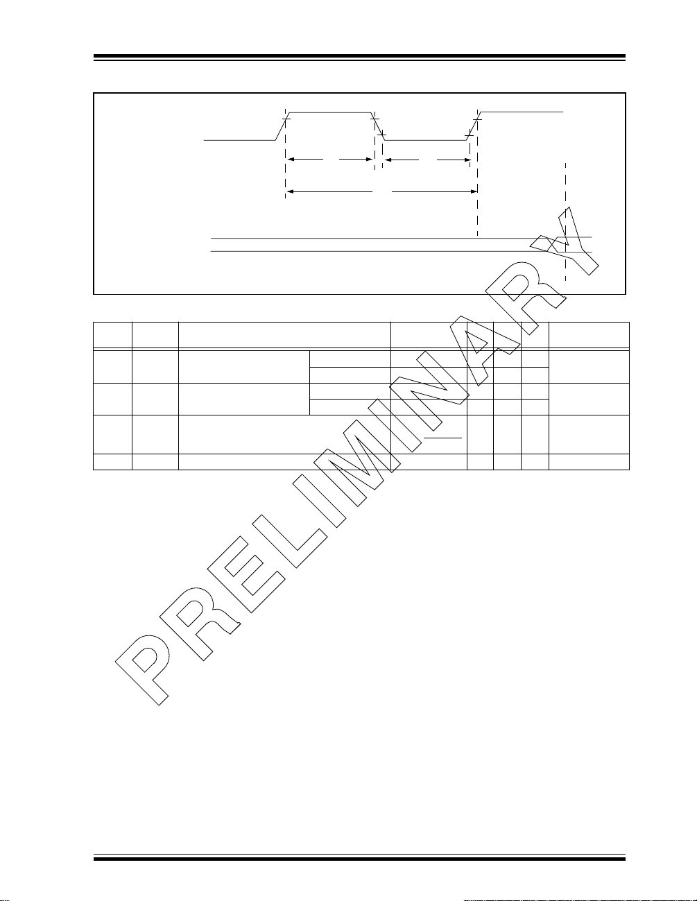
FIGURE 12-5: TIMER0 CLOCK TIMINGS
GP2/T0CKI
PIC12CE67X
40
41
42
TMR0
Note: Refer to Figure 12-1 for load conditions.
TABLE 12-5: TIMER0 CLOCK REQUIREMENTS
Param
Sym Characteristic Min Typ† Max Units Conditions
No.
40
Tt0H T0CKI High Pulse Width No Prescaler 0.5TCY + 20* — — ns
With Prescaler 10* — — ns
41 Tt0L T0CKI Low Pulse Width No Prescaler 0.5TCY + 20* — — ns
With Prescaler 10* — — ns
42 Tt0P T0CKI Period Greater of:
20µs or TCY + 40*
N
48 Tcke2tmrI Delay from external clock edge to timer increment 2Tosc — 7Tosc —
* These parameters are characterized but not tested.
† Data in "Typ" column is at 5V, 25°C unless otherwise stated. These parameters are for design guidance only and are not
tested.
— — ns N = prescale value
(1, 2, 4,..., 256)
1998 Microchip Technology Inc. Preliminary DS40181A-page 89

PIC12CE67X
TABLE 12-6: GPIO PULL-UP RESISTOR RANGES
VDD (Volts) Temperature (°C) Min Typ Max Units
GP0/GP1
2.5 –40 38K 42K 63K Ω
25 42K 48K 63K Ω
85 42K 49K 63K Ω
125 50K 55K 63K Ω
3.0 –40 28K 32K 43K Ω
25 34K 38K 43K Ω
85 34K 40K 43K Ω
125 38K 40K 43K Ω
5.5 –40 15K 17K 20K Ω
25 18K 20K 23K Ω
85 19K 22K 25K Ω
125 22K 24K 28K Ω
GP3
2.5 –40 285K 346K 417K Ω
25 343K 414K 532K Ω
85 368K 457K 532K Ω
125 431K 504K 593K Ω
3.0 –40 270K 326K 396K Ω
25 327K 389K 472K Ω
85 349K 427K 500K Ω
125 400K 472K 566K Ω
5.5 –40 247K 292K 360K Ω
25 288K 341K 437K Ω
85 306K 371K 448K Ω
125 351K 407K 500K Ω
* These parameters are characterized but not tested.
DS40181A-page 90 Preliminary 1998 Microchip Technology Inc.

PIC12CE67X
TABLE 12-7: A/D CONVERTER CHARACTERISTICS:
PIC12CE673-04 (COMMERCIAL, INDUSTRIAL, EXTENDED
PIC12CE673-10 (COMMERCIAL, INDUSTRIAL, EXTENDED
PIC12CE674-04 (COMMERCIAL, INDUSTRIAL, EXTENDED
PIC12CE674-10 (COMMERCIAL, INDUSTRIAL, EXTENDED
Parameter
No.
Note 1: When A/D is off, it will not consume any current other than minor leakage current. The power-down current spec includes
Sym Characteristic Min Typ† Max Units Conditions
NR Resolution — — 8-bits — VREF = VDD = 5.12V, VSS ≤ AIN ≤ VREF
NINT Integral error — — less than
NDIF Differential error — — less than
NFS Full scale error — — less than
NOFF Offset error — — less than
— Monotonicity — guaranteed — — VSS ≤ AIN ≤ VREF
VREF Reference voltage 3.0V — VDD + 0.3 V
VAIN Analog input voltage VSS - 0.3 — VREF + 0.3 V
ZAIN Recommended
impedance of analog
voltage source
IAD A/D conversion cur-
rent (VDD)
IREF VREF input current
(Note 2)
* These parameters are characterized but not tested.
† Data in “Typ” column is at 5V, 25°C unless otherwise stated. These parameters are for design guidance only and are not
tested.
any such leakage from the A/D module.
2: VREF current is from GP1 pin or VDD pin, whichever is selected as reference input.
3: Extended operating range is Advance Information for this device.
— — 10.0 kΩ
— 180 — µA Average current consumption when
— — 1
±1 LSb
±1 LSb
±1 LSb
±1 LSb
10
(3)
)
(3)
)
(3)
)
(3)
)
— VREF = VDD = 5.12V, VSS ≤ AIN ≤ VREF
— VREF = VDD = 5.12V, VSS ≤ AIN ≤ VREF
— VREF = VDD = 5.12V, VSS ≤ AIN ≤ VREF
— VREF = VDD = 5.12V, VSS ≤ AIN ≤ VREF
A/D is on. (Note 1)
mAµADuring sampling
All other times
1998 Microchip Technology Inc. Preliminary DS40181A-page 91

PIC12CE67X
TABLE 12-8: A/D CONVERTER CHARACTERISTICS:
PIC12LCE673-04 (COMMERCIAL, INDUSTRIAL)
PIC12LCE674-04 (COMMERCIAL, INDUSTRIAL)
Parameter
No.
Note 1: These specifications apply if VREF = 3.0V and if VDD ≥ 3.0V. VIN must be between VSS and VREF
Sym Characteristic Min Typ† Max Units Conditions
NR Resolution — — 8-bits — VREF = VDD = 3.0V (Note 1)
NINT Integral error — — less than
NDIF Differential error — — less than
NFS Full scale error — — less than
NOFF Offset error — — less than
— Monotonicity — guaranteed — — VSS ≤ AIN ≤ VREF
VREF Reference voltage 3.0V — VDD + 0.3 V
VAIN Analog input voltage VSS - 0.3 — VREF + 0.3 V
ZAIN Recommended
impedance of analog voltage source
IAD A/D conversion cur-
rent (VDD)
IREF VREF input current
(Note 3)
* These parameters are characterized but not tested.
† Data in “Typ” column is at 5V, 25°C unless otherwise stated. These parameters are for design guidance only and are not
tested.
2: When A/D is off, it will not consume any current other than minor leakage current. The power-down current spec includes
any such leakage from the A/D module.
3: VREF current is from GP1 pin or VDD pin, whichever is selected as reference input.
— — 10.0 kΩ
— 90 — µA Average current consumption when
— — 1
±1 LSb
±1 LSb
±1 LSb
±1 LSb
10
— VREF = VDD = 3.0V (Note 1)
— VREF = VDD = 3.0V (Note 1)
— VREF = VDD = 3.0V (Note 1)
— VREF = VDD = 3.0V (Note 1)
A/D is on. (Note 2)
mAµADuring sampling
All other times
DS40181A-page 92 Preliminary 1998 Microchip Technology Inc.

FIGURE 12-6: A/D CONVERSION TIMING
PIC12CE67X
BSF ADCON0, GO
Q4
A/D CLK
A/D DATA
ADRES
ADIF
GO
SAMPLE
132
(1)
OSC/2)
(T
7 6 5 4 3 2 1 0
OLD_DATA
131
130
SAMPLING STOPPED
1 Tcy
NEW_DATA
DONE
Note 1: If the A/D clock source is selected as RC, a time of TCY is added before the A/D clock starts. This allows the
SLEEP instruction to be executed.
TABLE 12-9: A/D CONVERSION REQUIREMENTS
Parameter
No.
130 TAD A/D clock period 1.6
130 TAD A/D Internal RC
131 TCNV Conversion time
132 TACQ Acquisition time Note 2 20 — µs
Note 1: ADRES register may be read on the following TCY cycle.
Sym Characteristic Min Typ† Max Units Conditions
—
2.0
—
µsµsVREF ≥ 3.0V
VREF full range
ADCS1:ADCS0 = 11
Oscillator source
3.0 6.0 9.0 µs
(RC oscillator source)
PIC12LCE67X, V
DD = 3.0V
2.0 4.0 6.0 µs PIC12CE67X
— 9.5TAD — —
(not including S/H
time). Note 1
* These parameters are characterized but not tested.
† Data in “Typ” column is at 5V, 25°C unless otherwise stated. These parameters are for design guidance only and are not
tested.
1998 Microchip Technology Inc. Preliminary DS40181A-page 93

PIC12CE67X
NOTES:
DS40181A-page 94 Preliminary 1998 Microchip Technology Inc.

PIC12CE67X
13.0 DC AND AC CHARACTERISTICS - PIC12CE67X
The graphs and tables provided in this section are for design guidance and are not tested or guaranteed. In some
graphs or tables the data presented are outside specified operating range (e.g., outside specified V
for information only and devices will operate properly only within the specified range.
The data presented in this section is a statistical summary of data collected on units from different lots over a period of
time. “Typical” represents the mean of the distribution while “max” or “min” represents (mean + 3σ) and (mean – 3σ)
respectively, where σ is standard deviation.
FIGURE 13-1: CALIBRATED INTERNAL RC FREQUENCY RANGE VS. TEMPERATURE (VDD = 5.0V)
(INTERNAL RC IS CALIBRATED TO 25°C, 5.0V)
4.2
4.15
4.1
4.05
4.0
3.95
3.9
Frequency (MHz)
3.85
3.8
3.75
3.7
-40 25 85
Temperature (°C)
DD range). This is
125
FIGURE 13-2: CALIBRATED INTERNAL RC FREQUENCY RANGE VS. TEMPERATURE (V
DD = 3.0V)
(INTERNAL RC IS CALIBRATED TO 25°C, 5.0V)
4.1
4.0
3.9
3.8
Frequency (MHz)
3.7
3.6
3.5
-40 25 85
Temperature (°C)
1998 Microchip Technology Inc. Preliminary DS40181A-page 95
125

PIC12CE67X
FIGURE 13-3: INTERNAL RC FREQUENCY VS. CALIBRATION VALUE (VDD = 5.5V)
4.80
4.65
4.50
4.35
4.20
4.05
3.90
Frequency (MHz)
3.75
3.60
3.45
3.30
00 10 20 30 40 50 60 70 80 90 A0 B0 C0 D0 E0 F0
-40°C
+25°C
+85°C
+125°C
OSCCAL Value (Hex)
FIGURE 13-4: INTERNAL RC FREQUENCY VS. CALIBRATION VALUE (V
4.80
4.65
4.50
4.35
4.20
4.05
3.90
Frequency (MHz)
3.75
3.60
3.45
3.30
00 10 20 30 40 50 60 70 80 90 A0 B0 C0 D0 E0 F0
-40°C
+25°C
+85°C
+125°C
OSCCAL Value (Hex)
DD = 3.5V)
DS40181A-page 96 Preliminary 1998 Microchip Technology Inc.

PIC12CE67X
TABLE 13-1: DYNAMIC IDD (TYPICAL) - WDT ENABLED, 25°C
Oscillator Frequency VDD = 2.5V VDD = 5.5V
External RC 4 MHz 250 µA* 620 µA*
Internal RC 4 MHz 420 µA 1.1 mA
XT 4 MHz 251 µA 775 µA
LP 32 KHz 7 µA 37 µA
*Does not include current through external R&C.
FIGURE 13-5: WDT TIMER TIME-OUT
PERIOD vs. VDD
50
45
40
35
30
25
WDT period (µs)
20
15
10
5
2 3 4 5 6 7
V
DD (Volts)
Max +125°C
Max +85°C
Typ +25°C
MIn –40°C
DS40181A-page 97 Preliminary 1998 Microchip Technology Inc.

PIC12CE67X
FIGURE 13-6: IOH vs. VOH, VDD = 2.5 V
0
-1
-2
-3
IOH (mA)
-4
-5
Max –40°C
Typ +25°C
-6
Min +125°C
Min +85°C
-7
500m 1.0 1.5
2.0 2.5
VOH (Volts)
FIGURE 13-7: IOH vs. VOH, VDD = 3.5 V
0
FIGURE 13-8: IOL vs. VOL, VDD = 2.5 V
25
20
Max –40°C
15
Typ +25°C
IOL (mA)
10
Min +85°C
5
Min +125°C
0
0
250.0m 500.0m 1.0
OL (Volts)
V
FIGURE 13-9: IOL vs. VOL, VDD = 3.5 V
IOH (mA)
-10
-13
-15
-18
-20
-3
-5
-8
Typ +25°C
2.0 2.5
3.01.5
.50
Max –40°C
Min +125°C
Min +85°C
IOL (mA)
40
30
20
10
Max –40°C
Typ +25°C
Min +85°C
Min +125°C
0
0
.50 .75 1.0
VOH (Volts)
OL (Volts)
V
DS40181A-page 98 Preliminary 1998 Microchip Technology Inc.

PIC12CE67X
FIGURE 13-10: IOH vs. VOH, VDD = 5.5 V
0
-5
-10
-15
IOH (mA)
-20
Min +125°C
Min +85°C
-25
Typ +25°C
Max –40°C
-30
3.5 4.0 4.5
VOH (Volts)
5.0 5.5
FIGURE 13-11: IOL vs. VOL, VDD = 5.5 V
50
Max –40°C
Typ +25°C
Min +85°C
Min +125°C
IOL (mA)
40
30
20
10
0
.25
.50 .75 1.0
OL (Volts)
V
1998 Microchip Technology Inc. Preliminary DS40181A-page 99

PIC12CE67X
NOTES:
DS40181A-page 100 Preliminary 1998 Microchip Technology Inc.
 Loading...