

Microchip Technology Inc PIC12CE518T-04I-SM, PIC12CE519-04-JW, PIC12CE519-04-P, PIC12CE519-04E-P, PIC12CE519-04E-SM Datasheet
...
1997 Microchip Technology Inc.
Preliminary
DS40172A-page 1
Devices:
PIC12CE518 and PIC12CE519 are 8-bit microcontrollers packaged in 8-lead packages. They are based on
the Enhanced PIC16C5X family.
High-Performance RISC CPU:
• Only 33 single word instructions to learn
• All instructions are single cycle (1 µs) except for
program branches which are two-cycle
• Operating speed: DC - 4 MHz clock input
DC - 1 µs instruction cycle
• 12-bit wide instructions
• 8-bit wide data path
• Special function hardware registers
• Two-level deep hardware stack
• Direct, indirect and relative addressing modes for
data and instructions
Peripheral Features:
• 8-bit real-time clock/counter (TMR0) with 8-bit
programmable prescaler
• 1,000,000 erase/write cycle EEPROM data
memory
• EEPROM data retention > 40 years
Device
Memory
EPROM
Program
RAM
Data
EEPROM
Data
PIC12CE518 512 x 12 25 x 8 16 x 8
PIC12CE519 1024 x 12 41 x 8 16 x 8
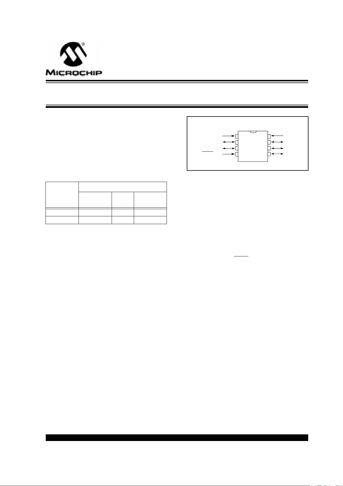
Pin Diagram:
Special Microcontroller Features:
• In-Circuit Serial Programming (ICSP™) of program memory (via two pins)
• Internal 4 MHz RC oscillator with programmable
calibration
• Power-on Reset (POR)
• Device Reset Timer (DRT)
• Watchdog Timer (WDT) with its own on-chip RC
oscillator for reliable operation
• Programmable code-protection
• Power saving SLEEP mode
• Wake-up from SLEEP on pin change
• Internal weak pull-ups on I/O pins
• Internal pull-up on MCLR
pin
• Selectable oscillator options:
- INTRC: Internal 4 MHz RC oscillator
- EXTRC: External low-cost RC oscillator
- XT: Standard crystal/resonator
- LP: Power saving, low frequency crystal
CMOS Tec hnology:
• Low-power, high-speed CMOS EPROM/
EEPROM technology
• Fully static design
• Wide temperature range:
- Commercial: 0°C to +70°C
- Industrial: -40°C to +85°C
- Extended: -40°C to +125°C
• Wide operating voltage range:
-Commercial: 3.0V to 5.5V
-Industrial: 3.0V to 5.5V
-Extended: 4.5V to 5.5V
• Low power consumption
- < 2 mA typical @ 5V, 4 MHz
- 15 µA typical @ 3V, 32 kHz
- < 1 µA typical standby current
PDIP, SOIC, Windowed CERDIP
8
7
6
5
1
2
3
4
PIC12CE518
VSS
GP0
GP1
GP2/T0CKI
PIC12CE519
GP5/OSC1/CLKIN
GP4/OSC2
GP3/MCLR
/VPP
VDD
PIC12CE5XX
8-Pin, 8-Bit CMOS Microcontroller with
EEPROM Data Memory
12CF5XX_GEBook Page 1 Tuesday, October 21, 1997 8:23 AM

PIC12CE5XX
DS40172A-page 2
Preliminary
1997 Microchip Technology Inc.
TABLE OF CONTENTS
1.0 General Description..................................................................................................................................................................... 3
2.0 PIC12CE5XX Device Varieties.................................................................................................................................................... 5
3.0 Architectural Overview ................................................................................................................................................................ 7
4.0 Memory Organization................................................................................................................................................................ 11
5.0 PIC12CE518I/O Port................................................................................................................................................................. 19
6.0 EEPROM Peripheral Operation................................................................................................................................................. 21
7.0 Timer0 Module and TMR0 Register.......................................................................................................................................... 25
8.0 Special Features of the CPU..................................................................................................................................................... 29
9.0 Instruction Set Summary........................................................................................................................................................... 41
10.0 Development Support................................................................................................................................................................ 53
11.0 Electrical Characteristics - PIC12CE5XX.................................................................................................................................. 57
12.0 DC and AC Characteristics - PIC12CE5XX .............................................................................................................................. 69
13.0 Packaging Information............................................................................................................................................................... 73
14.0 Appendix A................................................................................................................................................................................ 77
Index .................................................................................................................................................................................................... 83
PIC12CE5XX Product Identification System........................................................................................................................................ 87
To Our Valued Customers
We constantly strive to improve the quality of all our products and documentation. We have spent an exceptional
amount of time to ensure that these documents are correct. However, we realize that we may have missed a few
things. If you find any information that is missing or appears in error, please use the reader response form in the
back of this data sheet to inform us. We appreciate your assistance in making this a better document.
12CF5XX_GEBook Page 2 Tuesday, October 21, 1997 8:23 AM

1997 Microchip Technology Inc.
Preliminary
DS40172A-page 3
PIC12CE5XX
1.0 GENERAL DESCRIPTION
The 8-pin PIC12CE5XX from Microchip Technology is
a family of low-cost, high performance, 8-bit, fully static ,
EPROM/EEPROM-based CMOS microcontrollers. It
employs a RISC architecture with only 33 single word/
single cycle instructions. All instructions are single
cycle (1 µs) except for program branches which take
two cycles. The PIC12CE5XX delivers performance an
order of magnitude higher than its competitors in the
same price category. The 12-bit wide instructions are
highly symmetrical resulting in 2:1 code compression
over other 8-bit microcontrollers in its class. The easy
to use and easy to remember instruction set reduces
development time significantly.
The PIC12CE5XX products are equipped with special
features that reduce system cost and power requirements. The Power-On Reset (POR) and Device Reset
Timer (DRT) eliminate the need for external reset circuitry. There are four oscillator configurations to choose
from, including INTRC internal oscillator mode and the
power-saving LP (Low Power) oscillator. Power saving
SLEEP mode, Watchdog Timer and code protection
features improve system cost, power and reliability.
The PIC12CE5XX are available in the cost-effective
One-Time-Programmable (OTP) versions which are
suitable for production in any volume. The customer
can take full advantage of Microchip’s price leadership
in OTP microcontrollers while benefiting from the O TP’s
flexibility .
The PIC12CE5XX products are supported by a full-featured macro assembler, a software simulator, an in-circuit emulator, a ‘C’ compiler, fuzzy logic support tools,
a low-cost development programmer, and a full featured programmer. All the tools are supported on IBM
PC and compatible machines.
1.1 Applications
The PIC12CE5XX series fits perfectly in applications
ranging from sensory systems, gas detectors and
security systems to low-power remote transmitters/
receivers. The EPROM programming technology
makes customizing application programs (transmitter
codes, appliance settings, receiver frequencies, etc.)
extremely fast and convenient. While the EEPROM
data memory technology allows for the changing of calibrations factors and security codes, the small footprint
8-pin packages, for through hole or surface mounting,
make this microcontroller series perfect for applications
with space limitations. Low-cost, low-power, high performance, ease of use and I/O flexibility make the
PIC12CE5XX series very versatile even in areas where
no microcontroller use has been considered before
(e.g., timer functions, replacement of “glue” logic and
PLD’s in larger systems, coprocessor applications).
12CF5XX_GEBook Page 3 Tuesday, October 21, 1997 8:23 AM

PIC12CE5XX
DS40172A-page 4
Preliminary
1997 Microchip Technology Inc.
TABLE 1-1: PIC12CXXX FAMILY OF DEVICES
PIC12C508(A)
PIC12C509(A) PIC12CE518 PIC12CE519 PIC12C671 PIC12C672
Clock
Maximum Frequency
of Operation (MHz)
4 4 4 4 10 10
Memory
EPROM Program
Memory
512 x 12 1024 x 12 512 x 12 1024 x 12 1024 x 14 2048 x 14
RAM Data Memory
(bytes)
25 41 25 41 128 128
Peripherals
EEPROM Data Memory (bytes)
16 16
Timer Module(s) TMR0 TMR0 TMR0 TMR0 TMR0 TMR0
A/D Converter (8-bit)
Channels
— — — — 4 4
Features
Wake-up from
SLEEP on
pin change
Yes Yes Yes Yes Yes Yes
Interrupt Sources — — 4 4
I/O Pins 5 5 5 5 5 5
Input Pins 1 1 1 1 1 1
Internal Pull-ups Yes Yes Yes Yes Yes Yes
In-Circuit Serial Pro-
gramming
Yes Yes Yes Yes Yes Yes
Number of Instructions
33 33 33 33 35 35
Packages 8-pin DIP,
JW, SOIC
8-pin DIP,
JW, SOIC
8-pin DIP,
JW, SOIC
8-pin DIP,
JW, SOIC
8-pin DIP,
JW, SOIC
8-pin DIP,
JW, SOIC
All PIC12CE5XX devices have Power-on Reset, selectable Watchdog Timer, selectable code protect and high I/O current capability.
All PIC12CE5XX devices use serial programming with data pin GP0 and clock pin GP1.
12CF5XX_GEBook Page 4 Tuesday, October 21, 1997 8:23 AM

1997 Microchip Technology Inc.
Preliminary
DS40172A-page 5
PIC12CE5XX
2.0 PIC12CE5XX DEVICE
VARIETIES
A variety of packaging options are available.
Depending on application and production
requirements, the proper device option can be
selected using the information in this section. When
placing orders, please use the PIC12CE5XX Product
Identification System at the back of this data sheet to
specify the correct part number.
2.1 UV Erasab
le Devices
The UV erasable version, offered in windowed cerdip
package, is optimal for prototype development and
pilot programs.
The UV erasable version can be erased and
reprogrammed to any of the configuration modes.
Microchip's PICST ART
PLUS and PRO MATE programmers all support programming of the
PIC12CE5XX. Third party programmers also are available; refer to the
Microchip Third Party Guide
for a list
of sources.
2.2 O
ne-Time-Programmable (OTP)
Devices
The availability of OTP devices is especially useful for
customers who need the flexibility for frequent code
updates or small volume applications.
The OTP devices , packaged in plastic pac kages permit
the user to program them once. In addition to the
program memory, the configuration bits must also be
programmed.
Note:
Please note that erasing the device will
also erase the pre-programmed internal
calibration value for the inter nal oscillator.
The calibration value must be saved prior
to erasing the part.
2.3 Quic
k-Turnaround-Production (QTP)
Devices
Microchip offers a QTP Programming Service for
factory production orders. This service is made
available for users who choose not to program a
medium to high quantity of units and whose code
patterns have stabilized. The devices are identical to
the OTP devices b ut with all EPROM locations and fuse
options already programmed by the factory. Certain
code and prototype verification procedures do apply
before production shipments are availab le. Please contact your local Microchip Technology sales office for
more details.
2.4 Serializ
ed Quick-Turnaround
Production (SQTP
SM
) De
vices
Microchip offers a unique programming service where
a few user-defined locations in each device are
programmed with different serial numbers. The serial
numbers may be random, pseudo-random or
sequential.
Serial programming allows each device to have a
unique number which can serve as an entry-code,
password or ID number.
12CF5XX_GEBook Page 5 Tuesday, October 21, 1997 8:23 AM

PIC12CE5XX
DS40172A-page 6
Preliminary
1997 Microchip Technology Inc.
NOTES:
12CF5XX_GEBook Page 6 Tuesday, October 21, 1997 8:23 AM

1997 Microchip Technology Inc.
Preliminary
DS40172A-page 7
PIC12CE5XX
3.0 ARCHITECTURAL OVERVIEW
The high performance of the PIC12CE5XX family can
be attributed to a number of architectural features
commonly found in RISC microprocessors. To begin
with, the PIC12CE5XX uses a Harvard architecture in
which program and data are accessed on separate
buses. This improves bandwidth over traditional von
Neumann architecture where program and data are
fetched on the same bus. Separating program and
data memory further allows instructions to be sized
differently than the 8-bit wide data word. Instruction
opcodes are 12-bits wide making it possible to have all
single word instructions. A 12-bit wide program
memory access bus fetches a 12-bit instruction in a
single cycle. A two-stage pipeline overlaps fetch and
execution of instructions. Consequently, all instructions
(33) execute in a single cycle (1µs @ 4MHz) except for
program branches.
The PIC12CE518 addresses 512 x 12 of program
memory, the PIC12CE519 addresses 1K x 12 of
program memory. All program memory is internal.
The PIC12CE5XX can directly or indirectly address its
register files and data memory. All special function
registers including the program counter are mapped in
the data memory. The PIC12CE5XX has a highly
orthogonal (symmetrical) instruction set that makes it
possible to carry out any operation on any register
using any addressing mode. This symmetrical nature
and lack of ‘special optimal situations’ make
programming with the PIC12CE5XX simple yet
efficient. In addition, the learning curve is reduced
significantly.
The PIC12CE5XX contains a 16 X 8 EEPROM
memory array for storing non-volatile information such
as calibration data or security codes. This memory
has an endurance of 1,000,000 erase/write cycles and
a retention of 40+ years.
The PIC12CE5XX device contains an 8-bit ALU and
working register. The ALU is a general purpose
arithmetic unit. It performs arithmetic and Boolean
functions between data in the working register and any
register file.
The ALU is 8-bits wide and capable of addition,
subtraction, shift and logical operations. Unless
otherwise mentioned, arithmetic operations are two's
complement in nature. In two-operand instructions,
typically one operand is the W (working) register. The
other operand is either a file register or an immediate
constant. In single operand instructions, the operand
is either the W register or a file register.
The W register is an 8-bit working register used for
ALU operations. It is not an addressable register.
Depending on the instruction executed, the ALU may
affect the values of the Carry (C), Digit Carry (DC),
and Zero (Z) bits in the STATUS register. The C and
DC bits operate as a borr
ow and digit borrow out bit,
respectively, in subtraction. See the
SUBWF
and
ADDWF
instructions for examples.
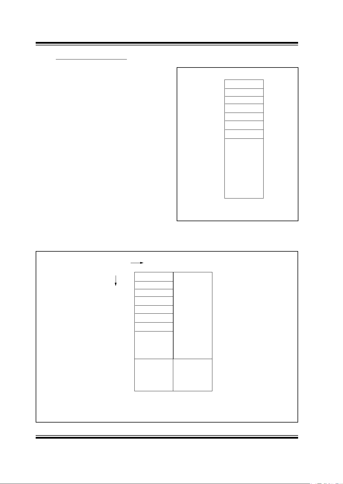
A simplified block diagram is shown in Figure 3-1, with
the corresponding device pins described in Table 3-1.
12CF5XX_GEBook Page 7 Tuesday, October 21, 1997 8:23 AM

PIC12CE5XX
DS40172A-page 8
Preliminary
1997 Microchip Technology Inc.
FIGURE 3-1: PIC12CE5XX BLOCK DIAGRAM
Device Reset
Timer
Power-on
Reset
Watchdog
Timer
EPROM
Program
Memory
12
Data Bus
8
12
Program
Bus
Instruction reg
Program Counter
RAM
File
Registers
Direct Addr
5
RAM Addr
9
Addr MUX
Indirect
Addr
FSR reg
STATUS reg
MUX
ALU
W reg
Instruction
Decode &
Control
Timing
Generation
OSC1/CLKIN
OSC2
MCLR
V
DD, VSS
Timer0
GPIO
8
8
GP4/OSC2
GP3/MCLR/VPP
GP2/T0CKI
GP1
GP0
5-7
3
GP5/OSC1/CLKIN
STACK1
STACK2
512 x 12 or
25 x 8 or
1024 x 12
41 x 8
Internal RC
OSC
16 X 8
EEPROM
Data
Memory
SCL
SDA
12CF5XX_GEBook Page 8 Tuesday, October 21, 1997 8:23 AM
1997 Microchip Technology Inc.
Preliminary
DS40172A-page 9
PIC12CE5XX
TABLE 3-1: PIC12CE5XX PINOUT DESCRIPTION
Name
DIP
Pin #
SOIC
Pin #
I/O/P
Type
Buffer
Type
Description
GP0 7 7 I/O TTL/ST Bi-directional I/O port/ serial programming data. Can
be software programmed for internal weak pull-up and
wake-up from SLEEP on pin change. This buffer is a
Schmitt Trigger input when used in serial programming
mode.
GP1 6 6 I/O TTL/ST Bi-directional I/O port/ serial programming clock. Can
be software programmed for internal weak pull-up and
wake-up from SLEEP on pin change. This buffer is a
Schmitt Trigger input when used in serial programming
mode.
GP2/T0CKI 5 5 I/O ST Bi-directional I/O port. Can be configured as T0CKI.
GP3/MCLR
/V
PP
4 4 I TTL Input port/master clear (reset) input/programming volt-
age input. When configured as MCLR
, this pin is an
active low reset to the device. Voltage on MCLR
/VPP
must not exceed VDD during normal device operation.
Can be software programmed for internal weak pull-up
and wake-up from SLEEP on pin change. Weak pullup always on if configured as MCLR
GP4/OSC2 3 3 I/O TTL Bi-directional I/O port/oscillator crystal output. Con-
nections to crystal or resonator in crystal oscillator
mode (XT and LP modes only, GPIO in other modes).
GP5/OSC1/CLKIN 2 2 I/O TTL/ST Bidirectional IO port/oscillator crystal input/external
clock source input (GPIO in Internal RC mode only,
OSC1 in all other oscillator modes). TTL input when
GPIO, ST input in external RC oscillator mode.
V
DD
1 1 P — Positive supply for logic and I/O pins
V
SS
8 8 P — Ground reference for logic and I/O pins
Legend: I = input, O = output, I/O = input/output, P = power, — = not used, TTL = TTL input,
ST = Schmitt Trigger input
12CF5XX_GEBook Page 9 Tuesday, October 21, 1997 8:23 AM
PIC12CE5XX
DS40172A-page 10
Preliminary
1997 Microchip Technology Inc.
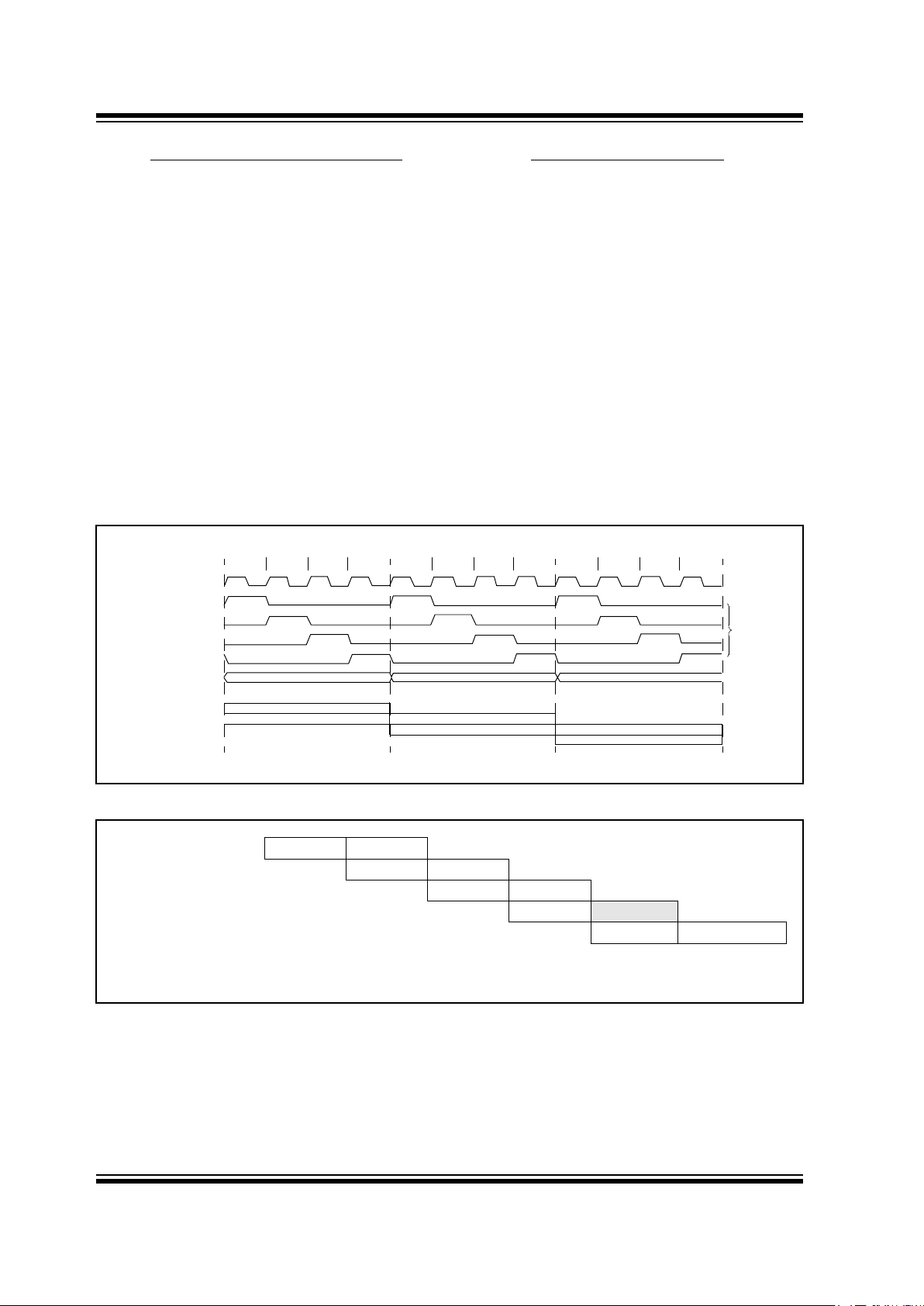
3.1 Cloc
king Scheme/Instruction Cycle
The clock input (OSC1/CLKIN pin) is internally divided
by four to generate four non-overlapping quadrature
clocks namely Q1, Q2, Q3 and Q4. Internally, the
program counter is incremented every Q1, and the
instruction is fetched from program memory and
latched into instruction register in Q4. It is decoded
and executed during the following Q1 through Q4. The
clocks and instruction execution flow is shown in
Figure 3-2 and Example 3-1.
3.2 Instruction Flo
w/Pipelining
An Instruction Cycle consists of four Q cycles (Q1, Q2,
Q3 and Q4). The instruction fetch and execute are
pipelined such that fetch takes one instruction cycle
while decode and execute takes another instruction
cycle. However, due to the pipelining, each instruction
effectively executes in one cycle. If an instruction
causes the program counter to change (e.g.,
GOTO
)
then two cycles are required to complete the
instruction (Example 3-1).
A fetch cycle begins with the program counter (PC)
incrementing in Q1.
In the execution cycle, the fetched instruction is
latched into the Instruction Register (IR) in cycle Q1.
This instruction is then decoded and executed during
the Q2, Q3, and Q4 cycles. Data memory is read
during Q2 (operand read) and written during Q4
(destination write).
FIGURE 3-2: CLOCK/INSTRUCTION CYCLE
EXAMPLE 3-1: INSTRUCTION PIPELINE FLOW
Q1
Q2 Q3 Q4
Q1
Q2 Q3 Q4
Q1
Q2 Q3 Q4
OSC1
Q1
Q2
Q3
Q4
PC
PC PC+1 PC+2
Fetch INST (PC)
Execute INST (PC-1) Fetch INST (PC+1)
Execute INST (PC) Fetch INST (PC+2)
Execute INST (PC+1)
Internal
phase
clock
All instructions are single cycle, except for any program branches. These take two cycles since the fetch
instruction is “flushed” from the pipeline while the new instruction is being fetched and then executed.
1. MOVLW 03H
Fetch 1 Execute 1
2. MOVWF GPIO
Fetch 2 Execute 2
3. CALL SUB_1
Fetch 3 Execute 3
4. BSF GPIO, BIT1
Fetch 4 Flush
Fetch SUB_1 Execute SUB_1
12CF5XX_GEBook Page 10 Tuesday, October 21, 1997 8:23 AM
1997 Microchip Technology Inc.
Preliminary
DS40172A-page 11
PIC12CE5XX
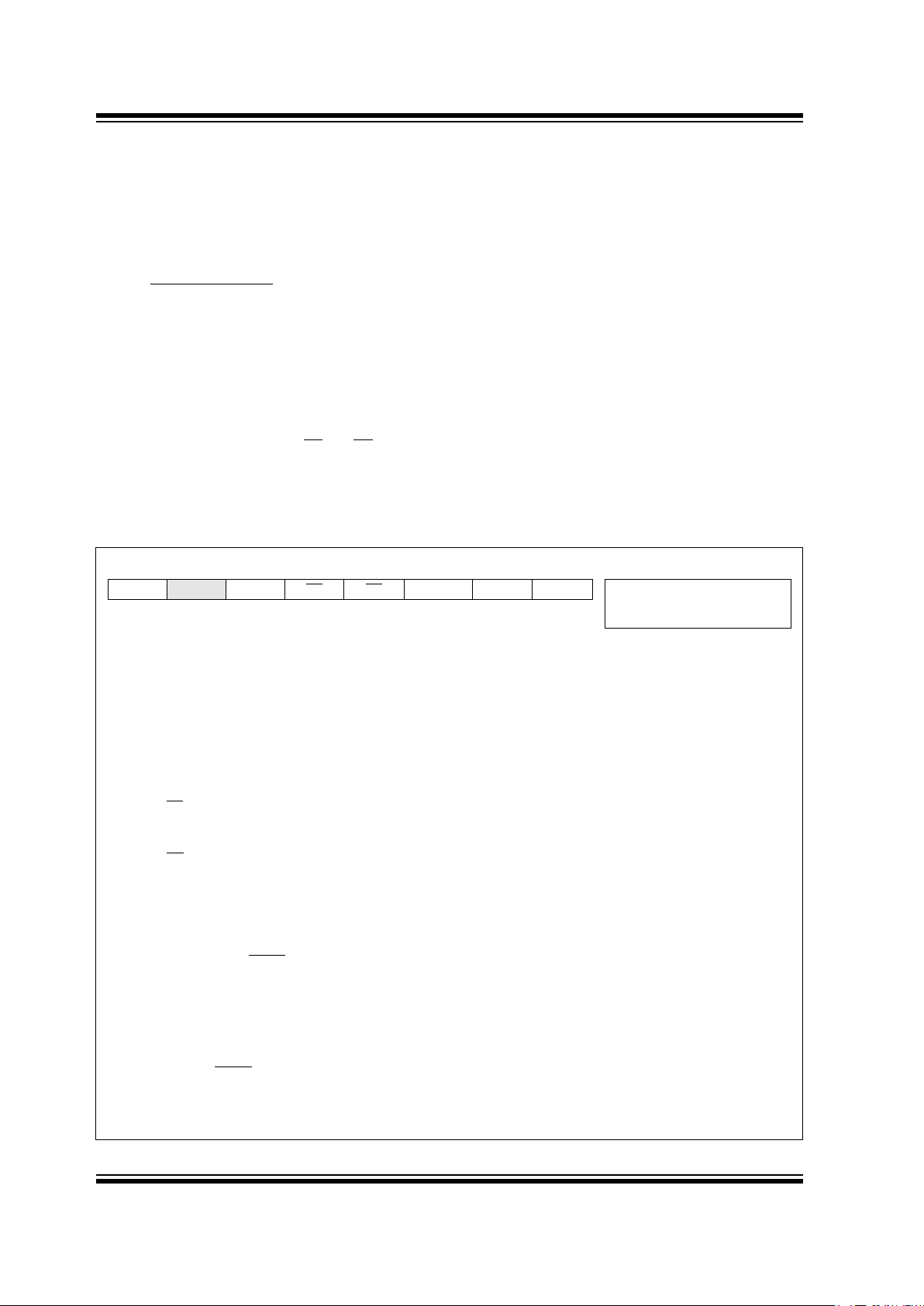
4.0 MEMORY ORGANIZATION
PIC12CE5XX memory is organized into program memory and data memory. For devices with more than 512
bytes of program memory, a paging scheme is used.
Program memory pages are accessed using one STATUS register bit. For the PIC12CE519 with a data
memory register file of more than 32 registers, a banking scheme is used. Data memory banks are accessed
using the File Select Register (FSR).
4.1 Pr
ogram Memory Organization
The PIC12CE5XX devices have a 12-bit Program
Counter (PC) capable of addressing a 2K x 12
program memory space.
Only the first 512 x 12 (0000h-01FFh) for the
PIC12CE518 and 1K x 12 (0000h-03FFh) for the
PIC12CE519 are physically implemented. Refer to
Figure 4-1. Accessing a location above these
boundaries will cause a wrap-around within the first
512 x 12 space (PIC12CE518) or 1K x 12 space
(PIC12CE519). The effective reset vector is at 000h,
(see Figure 4-1). Location 01FFh (PIC12CE518) or
location 03FFh (PIC12CE519), the hardwired reset
vector location, contains the internal clock oscillator
calibration value. This value is set at Microchip and
should never be overwritten. Upon reset, the
MOVLW XX is executed, the PC wraps to location
0000h, thus making 0000h the effective reset vector.
FIGURE 4-1: PROGRAM MEMORY MAP
AND STACK FOR THE
PIC12CE5XX
CALL, RETLW
PC<11:0>
Stack Level 1
Stack Level 2
User Memory
Space
12
0000h
7FFh
01FFh
0200h
On-chip Program
Memory
Reset Vector (note 1)
Note 1: Address 0000h becomes the
effective reset vector. Location
01FFh (PIC12CE518) or location
03FFh (PIC12CE519) contains the
MOVLW XX INTRC oscillator
calibration value.
512 Word (PIC12CE518)
1024 Word (PIC12CE519)
03FFh
0400h
On-chip Program
Memory
12CF5XX_GEBook Page 11 Tuesday, October 21, 1997 8:23 AM
PIC12CE5XX
DS40172A-page 12
Preliminary
1997 Microchip Technology Inc.
4.2 Data Memor
y Organization
Data memory is composed of registers, or bytes of
RAM. Therefore, data memory for a device is specified
by its register file. The register file is divided into two
functional groups: special function registers and
general purpose registers.
The special function registers include the TMR0
register, the Program Counter (PC), the Status
Register, the I/O registers (ports), and the File Select
Register (FSR). In addition, special purpose registers
are used to control the I/O port configuration and
prescaler options.
The general purpose registers are used for data and
control information under command of the instructions.
For the PIC12CE518, the register file is composed of 7
special function registers and 25 general purpose
registers (Figure 4-2).
For the PIC12CE519, the register file is composed of 7
special function registers, 25 general purpose
registers, and 16 general purpose registers that may
be addressed using a banking scheme (Figure 4-3).
4.2.1 GENERAL PURPOSE REGISTER FILE
The general purpose register file is accessed either
directly or indirectly through the file select register
FSR (Section 4.8).
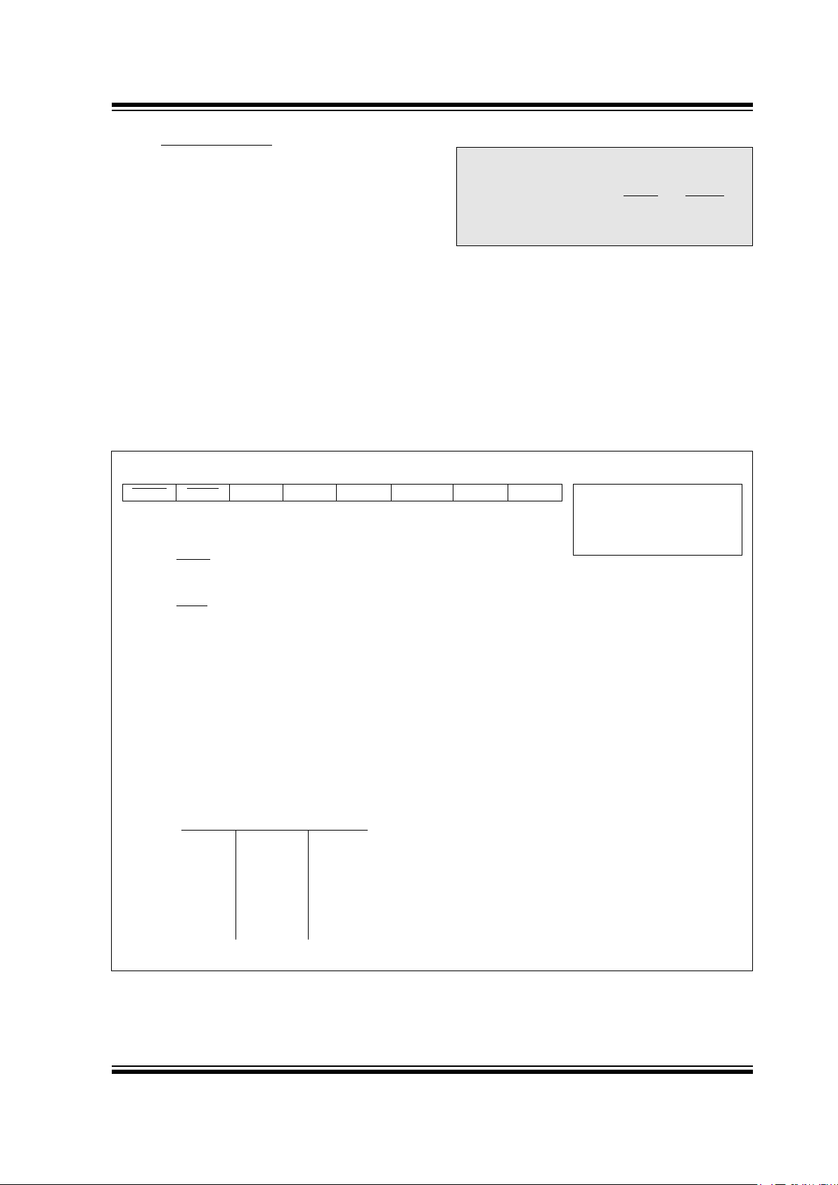
FIGURE 4-2: PIC12CE518 REGISTER FILE
MAP
File Address
00h
01h
02h
03h
04h
05h
06h
07h
1Fh
INDF
(1)
TMR0
PCL
STATUS
FSR
OSCCAL
GPIO
General
Purpose
Registers
Note 1: Not a physical register. See Indirect
Data Addressing, Section 4.8.
FIGURE 4-3: PIC12CE519 REGISTER FILE MAP
File Address
00h
01h
02h
03h
04h
05h
06h
07h
1Fh
INDF
(1)
TMR0
PCL
STATUS
FSR
OSCCAL
GPIO
0Fh
10h
Bank 0 Bank 1
3Fh
30h
20h
2Fh
General
Purpose
Registers
General
Purpose
Registers
General
Purpose
Registers
Addresses map
back to
addresses
in Bank 0.
Note 1: Not a physical register. See Indirect
Data Addressing, Section 4.8.
FSR<6:5> 00 01
12CF5XX_GEBook Page 12 Tuesday, October 21, 1997 8:23 AM
1997 Microchip Technology Inc.
Preliminary
DS40172A-page 13
PIC12CE5XX
4.2.2 SPECIAL FUNCTION REGISTERS
The Special Function Registers (SFRs) are registers
used by the CPU and peripheral functions to control
the operation of the device (Table 4-1).
The special registers can be classified into two sets.
The special function registers associated with the
“core” functions are described in this section. Those
related to the operation of the peripheral features are
described in the section for each peripheral feature.
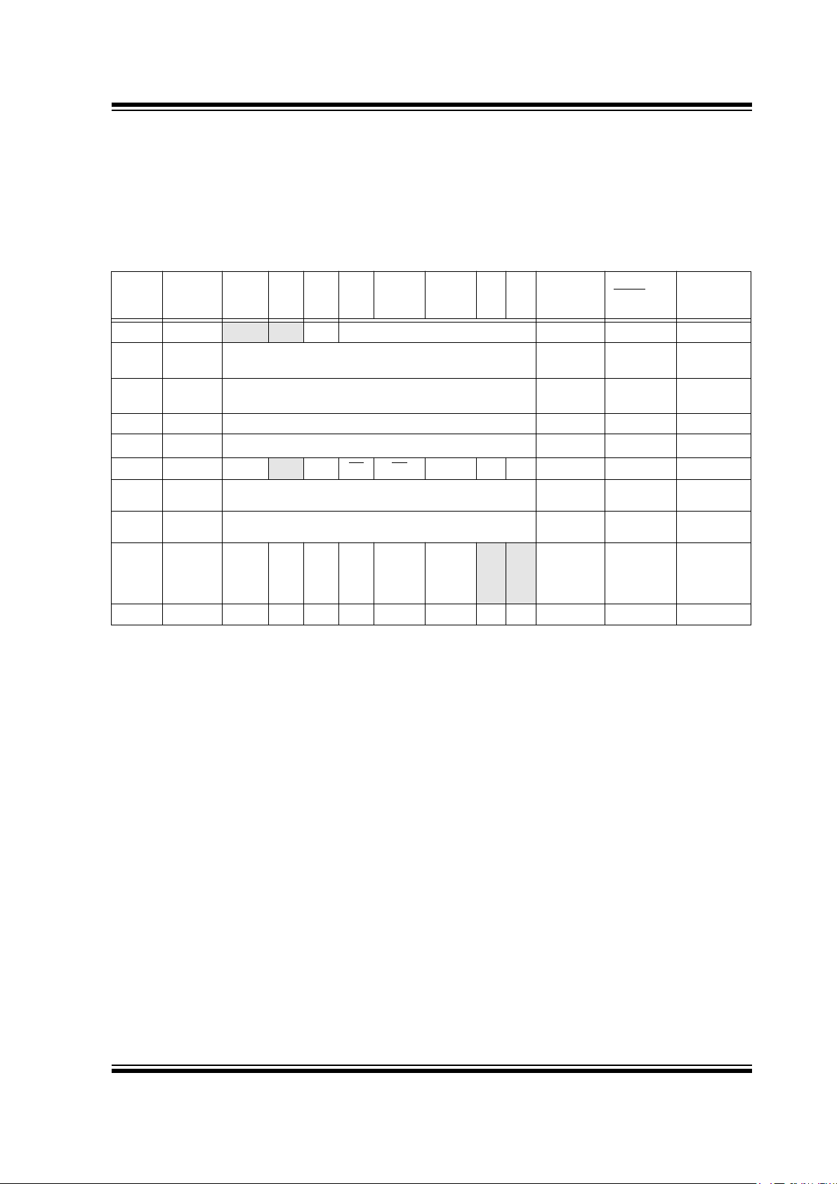
TABLE 4-1: SPECIAL FUNCTION REGISTER (SFR) SUMMARY
Address Name Bit 7 Bit 6 Bit 5 Bit 4 Bit 3 Bit 2 Bit 1 Bit 0
Value on
Power-On
Reset
Value on
M
CLR and
WDT Reset
Value on
Wake-up on
Pin Change
N/A TRIS
—
—
I/O control registers
--11 1111 --11 1111 --11 1111
N/A OPTION
Contains control bits to configure Timer0, Timer0/WDT
prescaler, wake-up on change, and weak pull-ups
1111 1111 1111 1111 1111 1111
00h INDF
Uses contents of FSR to address data memory (not a physical
register)
xxxx xxxx uuuu uuuu uuuu uuuu
01h TMR0 8-bit real-time clock/counter
xxxx xxxx uuuu uuuu uuuu uuuu
02h
(1)
PCL Low order 8 bits of PC
1111 1111 1111 1111 1111 1111
03h STATUS GPWUF
—
PA0 T
O PD Z DC C
0001 1xxx 000q quuu 100q quuu
04h
FSR
(12CE518)
Indirect data memory address pointer
111x xxxx 111u uuuu 111u uuuu
04h
FSR
(12CE519)
Indirect data memory address pointer
110x xxxx 11uu uuuu 11uu uuuu
05h
OSCCAL
(12CE518/
12CE519)
CAL7 CAL6 CAL5 CAL4 CALFST CALSLW — —
0111 00-- uuuu uu-- uuuu uu--
06h GPIO SCL SDA GP5 GP4 GP3 GP2 GP1 GP0 11xx xxxx 11uu uuuu 11uu uuuu
Legend: Shaded boxes = unimplemented or unused, — = unimplemented, read as '0' (if applicable)
x = unknown, u = unchanged, q = see the tables in Section 8.7 for possible values.
Note 1: The upper byte of the Program Counter is not directly accessible. See Section 4.6
for an explanation of how to access these bits.
12CF5XX_GEBook Page 13 Tuesday, October 21, 1997 8:23 AM
PIC12CE5XX
DS40172A-page 14 Preliminary 1997 Microchip Technology Inc.
4.2.3 EEPROM DATA MEMORY
The PIC12CE518 and PIC12CE519 each have 16
bytes of EEPROM data memory. The EEPROM data
memory supports a bi-directional 2-wire bus and data
transmission protocol. Refer to Section 6.0 on
EEPROM Peripherals.
4.3 STATUS Register
This register contains the arithmetic status of the ALU,
the RESET status, and the page preselect bit for
program memories larger than 512 words.
The STATUS register can be the destination for any
instruction, as with any other register. If the STATUS
register is the destination for an instruction that affects
the Z, DC or C bits, then the write to these three bits is
disabled. These bits are set or cleared according to
the device logic. Further more, the T
O and PD bits are
not writable. Therefore, the result of an instruction with
the STATUS register as destination may be different
than intended.
For example, CLRF STATUS will clear the upper three
bits and set the Z bit. This leaves the STATUS register
as 000u u1uu (where u = unchanged).
It is recommended, therefore, that only BCF, BSF and
MOVWF instructions be used to alter the STATUS
register because these instructions do not affect the Z,
DC or C bits from the STATUS register. For other
instructions, which do affect STATUS bits, see
Instruction Set Summary.
FIGURE 4-4: STATUS REGISTER (ADDRESS:03h)
R/W-0 R/W-0 R/W-0 R-1 R-1 R/W-x R/W-x R/W-x
GPWUF
—
PA0 TO PD Z DC C R = Readable bit
W = Writable bit
- n = Value at POR reset
bit7 6 5 4 3 2 1 bit0
bit 7: GPWUF: GPIO reset bit
1 = Reset due to wake-up from SLEEP on pin change
0 = After power up or other reset
bit 6: Unimplemented
bit 5: PA0: Program page preselect bits
1 = Page 1 (200h - 3FFh) - PIC12CE519
0 = Page 0 (000h - 1FFh) - PIC12CE518 and PIC12CE519
Each page is 512 bytes.
Using the PA0 bit as a general purpose read/write bit in devices which do not use it for program
page preselect is not recommended since this may affect upward compatibility with future products.
bit 4: TO: Time-out bit
1 = After power-up, CLRWDT instruction, or SLEEP instruction
0 = A WDT time-out occurred
bit 3: PD: Power-down bit
1 = After power-up or by the CLRWDT instruction
0 = By execution of the SLEEP instruction
bit 2: Z: Zero bit
1 = The result of an arithmetic or logic operation is zero
0 = The result of an arithmetic or logic operation is not zero
bit 1: DC: Digit carry/borrow bit (for ADDWF and SUBWF instructions)
ADDWF
1 = A carry from the 4th low order bit of the result occurred
0 = A carry from the 4th low order bit of the result did not occur
SUBWF
1 = A borrow from the 4th low order bit of the result did not occur
0 = A borrow from the 4th low order bit of the result occurred
bit 0: C: Carry/borrow bit (for ADDWF, SUBWF and RRF, RLF instructions)
ADDWF SUBWF RRF or RLF
1 = A carry occurred 1 = A borrow did not occur Load bit with LSB or MSB, respectively
0 = A carry did not occur 0 = A borrow occurred
12CF5XX_GEBook Page 14 Tuesday, October 21, 1997 8:23 AM
1997 Microchip Technology Inc. Preliminary DS40172A-page 15
PIC12CE5XX
4.4 OPTION Register
The OPTION register is a 8-bit wide, write-only
register which contains various control bits to
configure the Timer0/WDT prescaler and Timer0.
By executing the OPTION instruction, the contents of
the W register will be transferred to the OPTION
register. A RESET sets the OPTION<7:0> bits.
Note: If TRIS bit is set to ‘0’, the wake-up on
change and pull-up functions are disabled
for that pin; i.e., note that TRIS overrides
OPTION control of GPPU
and GPWU.
Note: If the T0CS bit is set to ‘1’, GP2 is f orced to
be an input even if TRIS GP2 = ‘0’.
FIGURE 4-5: OPTION REGISTER
W-1 W-1 W-1 W-1 W-1 W-1 W-1 W-1
GPWU GPPU T0CS T0SE PSA PS2 PS1 PS0 W = Writable bit
U = Unimplemented bit
- n = Value at POR reset
Reference Table 4-1 for
other resets.
bit7 6 5 4 3 2 1 bit0
bit 7: GPWU: Enable wake-up on pin change (GP0, GP1, GP3)
1 = Disabled
0 = Enabled
bit 6: GPPU: Enable weak pull-ups (GP0, GP1, GP3)
1 = Disabled
0 = Enabled
bit 5: T0CS: Timer0 clock source select bit
1 = Transition on T0CKI pin
0 = Transition on internal instruction cycle clock, Fosc/4
bit 4: T0SE: Timer0 source edge select bit
1 = Increment on high to low transition on the T0CKI pin
0 = Increment on low to high transition on the T0CKI pin
bit 3: PSA: Prescaler assignment bit
1 = Prescaler assigned to the WDT
0 = Prescaler assigned to Timer0
bit 2-0: PS2:PS0: Prescaler rate select bits
000
001
010
011
100
101
110
111
1 : 2
1 : 4
1 : 8
1 : 16
1 : 32
1 : 64
1 : 128
1 : 256
1 : 1
1 : 2
1 : 4
1 : 8
1 : 16
1 : 32
1 : 64
1 : 128
Bit Value Timer0 Rate WDT Rate
12CF5XX_GEBook Page 15 Tuesday, October 21, 1997 8:23 AM

PIC12CE5XX
DS40172A-page 16 Preliminary 1997 Microchip Technology Inc.
4.5 OSCCAL Register
The Oscillator Calibration (OSCCAL) register is used to
calibrate the internal 4 MHz oscillator. It contains four
bits for fine calibration and two other bits to either
increase or decrease frequency.
FIGURE 4-6: OSCCAL REGISTER (ADDRESS 8Fh)
R/W-0 R/W-1 R/W-1 R/W-1 R/W-0 R/W-0 U-0 U-0
CAL3 CAL2 CAL1 CAL0 CALFST CALSLW — — R = Readable bit
W = Writable bit
U = Unimplemented bit,
read as ‘0’
- n = Value at POR reset
bit7 bit0
bit 7-4: CAL<3:0>: Fine calibration
bit 3: CALFST: Calibration Fast
1 = Increase frequency
0 = No change
bit 2: CALSLW: Calibration Slow
1 = Decrease frequency
0 = No change
bit 1-0: Unimplemented: Read as '0'
Note: If CALFST = 1 and CALSLW = 1, CALFST has precedence.
12CF5XX_GEBook Page 16 Tuesday, October 21, 1997 8:23 AM
1997 Microchip Technology Inc. Preliminary DS40172A-page 17
PIC12CE5XX
4.6 Program Counter
As a program instruction is executed, the Program
Counter (PC) will contain the address of the next
program instruction to be executed. The PC value is
increased by one every instruction cycle, unless an
instruction changes the PC.
For a GOTO instruction, bits 8:0 of the PC are provided
by the GOTO instruction word. The PC Latch (PCL) is
mapped to PC<7:0>. Bit 5 of the STATUS register
provides page information to bit 9 of the PC (Figure 4-
7).
For a CALL instruction, or any instruction where the
PCL is the destination, bits 7:0 of the PC again are
provided by the instruction word. However, PC<8>
does not come from the instruction word, but is always
cleared (Figure 4-7).
Instructions where the PCL is the destination, or
Modify PCL instructions, include MOVWF PC, ADDWF
PC, and BSF PC,5.
FIGURE 4-7: LOADING OF PC
BRANCH INSTRUCTIONS PIC12CE518/CE519
Note: Because PC<8> is cleared in the CALL
instruction, or any Modify PCL instruction,
all subroutine calls or computed jumps are
limited to the first 256 locations of any program memory page (512 words long).
PA0
STATUS
PC
8 7 0
PCL
910
Instruction Word
7 0
GOTO Instruction
CALL or Modify PCL Instruction
11
PA0
STATUS
PC
8 7 0
PCL
910
Instruction Word
7 0
11
Reset to ‘0’
4.6.1 EFFECTS OF RESET
The Program Counter is set upon a RESET, which
means that the PC addresses the last location in the
last page i.e., the oscillator calibration instruction. After
executing MOVLW XX, the PC will roll over to location
00h, and begin executing user code.
The STATUS register page preselect bits are cleared
upon a RESET, which means that page 0 is preselected.
Therefore, upon a RESET, a GOTO instruction will
automatically cause the program to jump to page 0
until the value of the page bits is altered.
4.7 Stack
PIC12CE5XX devices have a 12-bit wide hardware
push/pop stack.
A CALL instruction will
push
the current value of stack
1 into stack 2 and then push the current program
counter value, incremented by one , into stac k le v el 1. If
more than two sequential CALL’s are executed, only
the most recent two return addresses are stored.
A RETLW instruction will
pop
the contents of stack level
1 into the program counter and then copy stack level 2
contents into level 1. If more than two sequential
RETLW’s are executed, the stack will be filled with the
address previously stored in level 2. Note that the
W register will be loaded with the literal value specified
in the instruction. This is particularly useful for the
implementation of data look-up tables within the
program memory.
12CF5XX_GEBook Page 17 Tuesday, October 21, 1997 8:23 AM
PIC12CE5XX
DS40172A-page 18 Preliminary 1997 Microchip Technology Inc.
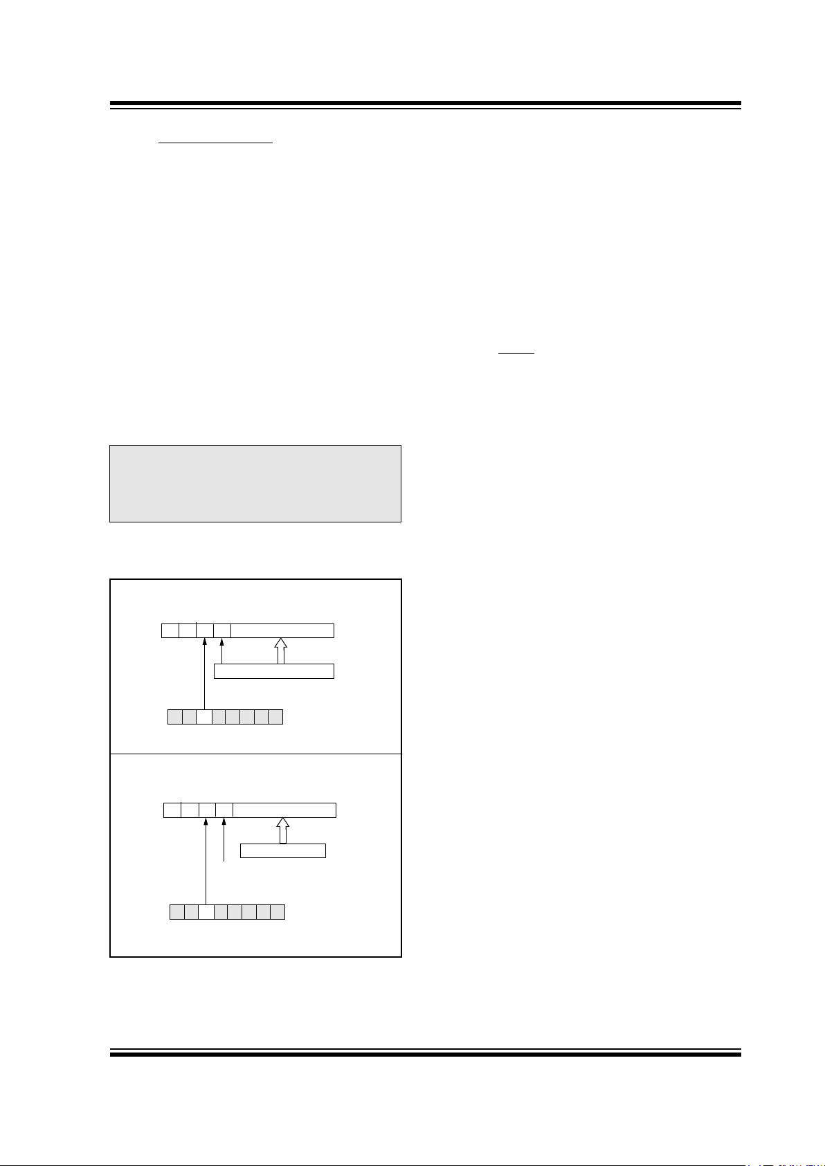
4.8 Indirect Data Addressing; INDF and
FSR Registers
The INDF register is not a physical register.
Addressing INDF actually addresses the register
whose address is contained in the FSR register (FSR
is a
pointer
). This is indirect addressing.
EXAMPLE 4-1: INDIRECT ADDRESSING
• Register file 07 contains the value 10h
• Register file 08 contains the value 0Ah
• Load the value 07 into the FSR register
• A read of the INDF register will return the value
of 10h
• Increment the value of the FSR register by one
(FSR = 08)
• A read of the INDR register now will return the
value of 0Ah.
Reading INDF itself indirectly (FSR = 0) will produce
00h. Writing to the INDF register indirectly results in a
no-operation (although STATUS bits may be affected).
A simple program to clear RAM locations 10h-1Fh
using indirect addressing is shown in Example 4-2.
EXAMPLE 4-2: HOW TO CLEAR RAM
USING INDIRECT
ADDRESSING
movlw 0x10 ;initialize pointer
movwf FSR ; to RAM
NEXT clrf INDF ;clear INDF register
incf FSR,F ;inc pointer
btfsc FSR,4 ;all done?
goto NEXT ;NO, clear next
CONTINUE
: ;YES, continue
The FSR is a 5-bit wide register. It is used in
conjunction with the INDF register to indirectly address
the data memory area.
The FSR<4:0> bits are used to select data memory
addresses 00h to 1Fh.
PIC12CE518: Does not use banking. FSR<6:5> are
unimplemented and read as '1's.
PIC12CE519: Uses FSR<5>. Selects between bank 0
and bank 1. FSR<6> is unimplemented, read as '1’ .
FIGURE 4-8: DIRECT/INDIRECT ADDRESSING
Note 1: For register map detail see Section 4.2.
Note 2: PIC12CE519 only
bank
location select
location select
bank select
Indirect Addressing
Direct Addressing
Data
Memory
(1)
0Fh
10h
Bank 0 Bank 1
(2)
0
4
5
6
(FSR)
00 01
00h
1Fh 3Fh
(opcode) 04
5
6
(FSR)
Addresses
map back to
addresses
in Bank 0.
12CF5XX_GEBook Page 18 Tuesday, October 21, 1997 8:23 AM
1997 Microchip Technology Inc. Preliminary DS40172A-page 19
PIC12CE5XX
5.0 PIC12CE518 I/O PORT
As with any other register, the I/O register can be
written and read under program control. However,
read instructions (e.g., MOVF GPIO,W) always read the
I/O pins independent of the pin’s input/output modes.
On RESET, all GPIO ports are defined as input (inputs
are at hi-impedance) since the I/O control registers are
all set.
5.1 GPIO
GPIO is an 8-bit I/O register. Only the low order 6 bits
are used (GP5:GP0) for pin control. Bits 6 and 7 (SDA
and SCL) are used by the EEPROM peripheral. Refer
to Section 6.0 and Appendix A for use of SDA and
SCL. Please note that GP3 is an input only pin. The
configuration word can set several I/O’s to alternate
functions. When acting as alternate functions the pins
will read as ‘0’ dur ing port read. Pins GP0, GP1, and
GP3 can be configured with weak pull-ups and also
with wake-up on change. The wake-up on change and
weak pull-up functions are not pin selectable. If pin 4 is
configured as MCLR
, weak pull-up is always on and
wake-up on change for this pin is not enabled.
5.2 TRIS Register
The output driver control register is loaded with the
contents of the W register by executing the TRIS f
instruction. A '1' from a TRIS register bit puts the
corresponding output driver in a hi-impedance mode.
A '0' puts the contents of the output data latch on the
selected pins, enabling the output buffer. The
exceptions are GP3 which is input only and GP2 which
may be controlled by the option register, see Figure 4-
5.
The TRIS registers are “write-only” and are set (output
drivers disabled) upon RESET.
Note: A read of the por ts reads the pins, not the
output data latches. That is, if an output
driver on a pin is enabled and driven high,
but the external system is holding it low, a
read of the port will indicate that the pin is
low.
5.3 I/O Interfacing
The equivalent circuit for an I/O port pin is shown in
Figure 5-1. All port pins, except GP3 which is input
only, may be used for both input and output
operations. For input operations these ports are nonlatching. Any input must be present until read by an
input instruction (e.g., MOVF GPIO,W). The outputs are
latched and remain unchanged until the output latch is
rewritten. To use a port pin as output, the
corresponding direction control bit in TRIS must be
cleared (= 0). For use as an input, the corresponding
TRIS bit must be set. Any I/O pin (except GP3) can be
programmed individually as input or output.
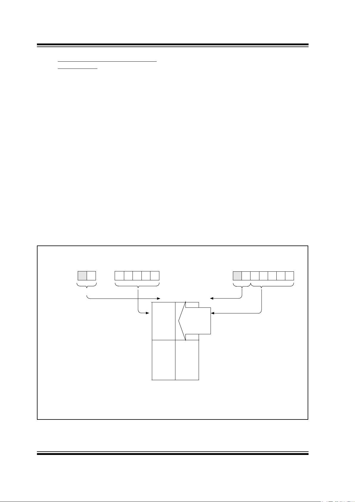
FIGURE 5-1: EQUIVALENT CIRCUIT
FOR A SINGLE I/O PIN
Note 1: I/O pins have protection diodes to VDD and VSS.
Data
Bus
QD
Q
CK
QD
Q
CK
P
N
WR
Port
TRIS ‘f’
Data
TRIS
RD Port
VSS
VDD
I/O
pin
(1)
W
Reg
Latch
Latch
Reset
TABLE 5-1: SUMMARY OF PORT REGISTERS
Address Name Bit 7 Bit 6 Bit 5 Bit 4 Bit 3 Bit 2 Bit 1 Bit 0
Value on
Power-On
Reset
Value on
MCLR and
WDT Reset
Value on
Wake-up on
Pin Change
N/A TRIS — — I/O control registers --11 1111 --11 1111 --11 1111
N/A
OPTION GPWU GPPU T0CS T0SE PSA PS2 PS1 PS0
1111 1111 1111 1111 1111 1111
03H
STATUS
GPWUF — PA0 TO PD Z DC C 0001 1xxx 000q quuu 100q quuu
06h
GPIO
SCL SDA GP5 GP4 GP3 GP2 GP1 GP0 11xx xxxx 11uu uuuu 11uu uuuu
Legend: Shaded cells not used by Port Registers, read as ‘0’, — = unimplemented, read as '0', x = unknown, u = unchanged,
q = see tables in Section 8.7 for possible values.
12CF5XX_GEBook Page 19 Tuesday, October 21, 1997 8:23 AM
PIC12CE5XX
DS40172A-page 20 Preliminary 1997 Microchip Technology Inc.
5.4 I/O Programming Considerations
5.4.1 BI-DIRECTIONAL I/O PORTS
Some instructions operate internally as read followed
by write operations. The BCF and BSF instructions, for
example, read the entire port into the CPU, execute
the bit operation and re-write the result. Caution must
be used when these instructions are applied to a port
where one or more pins are used as input/outputs. For
example, a BSF operation on bit5 of GPIO will cause all
eight bits of GPIO to be read into the CPU, bit5 to be
set and the GPIO value to be written to the output
latches. If another bit of GPIO is used as a bidirectional I/O pin (say bit0) and it is defined as an
input at this time, the input signal present on the pin
itself would be read into the CPU and rewritten to the
data latch of this particular pin, overwriting the
previous content. As long as the pin stays in the input
mode, no problem occurs. However, if bit0 is switched
into output mode later on, the content of the data latch
may now be unknown.
Example 5-1 shows the effect of two sequential readmodify-write instructions (e.g., BCF, BSF , etc.) on an I/
O port.
A pin actively outputting a high or a low should not be
driven from external devices at the same time in order
to change the level on this pin (“wired-or”, “wired-and”).
The resulting high output currents may damage the
chip.
EXAMPLE 5-1: READ-MODIFY-WRITE
INSTRUCTIONS ON AN
I/O PORT
;Initial GPIO Settings
; GPIO<5:3> Inputs
; GPIO<2:0> Outputs
;
; GPIO latch GPIO pins
; ---------- --------- BCF GPIO, 5 ;--01 -ppp --11 pppp
BCF GPIO, 4 ;--10 -ppp --11 pppp
MOVLW 007h ;
TRIS GPIO ;--10 -ppp --11 pppp
;
;Note that the user may have expected the pin
;values to be --00 pppp. The 2nd BCF caused
;GP5 to be latched as the pin value (High).
5.4.2 SUCCESSIVE OPERATIONS ON I/O
PORTS
The actual write to an I/O port happens at the end of
an instruction cycle, whereas for reading, the data
must be valid at the beginning of the instruction cycle
(Figure 5-2). Therefore, care must be exercised if a
write followed by a read operation is carried out on the
same I/O port. The sequence of instructions should
allow the pin voltage to stabilize (load dependent)
before the next instruction, which causes that file to be
read into the CPU, is executed. Otherwise, the
previous state of that pin may be read into the CPU
rather than the new state. When in doubt, it is better to
separate these instructions with a NOP or another
instruction not accessing this I/O port.
FIGURE 5-2: SUCCESSIVE I/O OPERATION
PC PC + 1 PC + 2
PC + 3
Q1 Q2
Q3
Q4
Q1 Q2
Q3
Q4
Q1 Q2
Q3
Q4
Q1 Q2
Q3
Q4
Instruction
fetched
GP5:GP0
MOVWF GPIO
NOP
Port pin
sampled here
NOP
MOVF GPIO,W
Instruction
executed
MOVWF GPIO
(Write to
GPIO)
NOP
MOVF GPIO,W
This example shows a write to GPIO followed
by a read from GPIO.
Data setup time = (0.25 TCY – TPD)
where: T
CY = instruction cycle.
TPD = propagation delay
Therefore, at higher clock frequencies, a
write followed by a read may be problematic.
(Read
GPIO)
Port pin
written here
12CF5XX_GEBook Page 20 Tuesday, October 21, 1997 8:23 AM

1997 Microchip Technology Inc. Preliminary DS40172A-page 21
PIC12CE5XX
6.0 EEPROM PERIPHERAL
OPERATION
The PIC12CE518 and PIC12CE519 each have 16
bytes of EEPROM data memory. The EEPROM memory has an endurance of 1,000,000 erase/write cycles
and a data retention of greater than 40 years. The
EEPROM data memory supports a bi-directional 2-wire
bus and data transmission protocol. These two-wires
are serial data (SDA) and serial clock (SCL), that are
mapped to bit6 and bit7, respectively, of the GPIO register (SFR 06h). Unlike the GP0-GP5 that are connected to the I/O pins, SDA and SCL are only
connected to the internal EEPROM peripheral. For
most applications, all that is required is calls to the following functions:
; Byte_Write: Byte write routine
; Inputs: EEPROM Address EEADDR
; EEPROM Data EEDATA
; Outputs: Return 01 in W if OK, else
return 00 in W
;
; Read_Current: Read EEPROM at address
currently held by EE device.
; Inputs: NONE
; Outputs: EEPROM Data EEDATA
; Return 01 in W if OK, else
return 00 in W
;
; Read_Random: Read EEPROM byte at supplied
address
; Inputs: EEPROM Address EEADDR
; Outputs: EEPROM Data EEDATA
; Return 01 in W if OK,
else return 00 in W
The code for these functions is listed in Appendix A,
and is accessed by either including the source code
EEPROM.INC or by linking EEPROM.ASM.
6.0.1 SERIAL DATA
SDA is a bi-directional pin used to transfer addresses
and data into and data out of the device.
For normal data transfer SD A is allowed to change only
during SCL low. Changes during SCL high are
reserved for indicating the START and STOP conditions.
6.0.2 SERIAL CLOCK
This SCL input is used to synchronize the data tr ansf er
from and to the device.
6.1 BUS CHARACTERISTICS
The following bus protocol is to be used with the
EEPROM data memory.
• Data transfer may be initiated only when the bus
is not busy.
During data transfer, the data line must remain stable
whenever the clock line is HIGH. Changes in the data
line while the clock line is HIGH will be interpreted as a
START or STOP condition.
Accordingly, the following bus conditions have been
defined (Figure 6-1).
6.1.1 BUS NOT BUSY (A)
Both data and clock lines remain HIGH.
6.1.2 START DATA TRANSFER (B)
A HIGH to LOW transition of the SDA line while the
clock (SCL) is HIGH determines a START condition. All
commands must be preceded by a START condition.
6.1.3 STOP DATA TRANSFER (C)
A LOW to HIGH transition of the SDA line while the
clock (SCL) is HIGH determines a STOP condition. All
operations must be ended with a STOP condition.
6.1.4 DATA VALID (D)
The state of the data line represents valid data when,
after a START condition, the data line is stable for the
duration of the HIGH period of the clock signal.
The data on the line must be changed during the LOW
period of the clock signal. There is one bit of data per
clock pulse.
Each data transfer is initiated with a START condition
and terminated with a STOP condition. The number of
the data bytes transferred between the START and
STOP conditions is determined by the master device
and is theoretically unlimited.
6.1.5 ACKNOWLEDGE
Each receiving device, when addressed, is obliged to
generate an acknowledge after the reception of each
byte. The master device must generate an extra clock
pulse which is associated with this acknowledge bit.
The device that acknowledges has to pull down the
SDA line during the acknowledge cloc k pulse in such a
way that the SDA line is stable LOW during the HIGH
period of the acknowledge related clock pulse. Of
course, setup and hold times must be taken into
account. A master must signal an end of data to the
slave by not generating an acknowledge bit on the last
byte that has been clocked out of the sla ve. In this case,
the slave must leave the data line HIGH to enable the
master to generate the STOP condition (Figure 6-2).
Note: Acknowledge bits are generated if an inter-
nal programming cycle is in progress.
12CF5XX_GEBook Page 21 Tuesday, October 21, 1997 8:23 AM
PIC12CE5XX
DS40172A-page 22 Preliminary 1997 Microchip Technology Inc.
FIGURE 6-1: DATA TRANSFER SEQUENCE ON THE SERIAL BUS
FIGURE 6-2: ACKNOWLEDGE TIMING
(A)
(B)
(C)
(D)
(A)(C)
SCL
SDA
START
CONDITION
ADDRESS OR
ACKNOWLEDGE
VALID
DATA
ALLOWED
TO CHANGE
STOP
CONDITION
SCL
987654321 1 2 3
Transmitter must release the SDA line at this point
allowing the Receiver to pull the SDA line low to
acknowledge the previous eight bits of data.
Receiver must release the SDA line at this point
so the Transmitter can continue sending data.
Data from transmitter
Data from transmitter
SDA
Acknowledge
Bit
6.2 Device Addressing
After generating a START condition, the bus master
transmits a control byte consisting of a slave address
and a Read/Wr
ite bit that indicates what type of operation is to be performed. The slave address consists of a
4-bit device code (1010) followed by three don't care
bits.
The last bit of the control byte determines the operation
to be performed. When set to a one a read operation is
selected, and when set to a zero a write operation is
selected. (Figure 6-3). The bus is monitored for its corresponding slave address all the time. It generates an
acknowledge bit if the slave address was true and it is
not in a programming mode.
FIGURE 6-3: CONTROL BYTE FORMAT
1 0 1 0 X X XS ACKR/W
Device Select
Bits
Don’t Care
Bits
Slave Address
Acknowledge Bit
Start Bit
Read/Wr
ite Bit
12CF5XX_GEBook Page 22 Tuesday, October 21, 1997 8:23 AM
1997 Microchip Technology Inc. Preliminary DS40172A-page 23
PIC12CE5XX
6.3 WRITE OPERATIONS
6.3.1 BYTE WRITE
Following the start signal from the master, the device
code (4 bits), the don't care bits (3 bits), and the R/W
bit (which is a logic low) are placed onto the bus by the
master transmitter. This indicates to the addressed
slave receiver that a b yte with a word address will follo w
after it has generated an acknowledge bit during the
ninth clock cycle. Therefore, the next byte transmitted
by the master is the word address and will be written
into the address pointer. Only the lower four address
bits are used by the device, and the upper four bits are
don’t cares. The address byte is acknowledgeable and
the master device will then transmit the data word to be
written into the addressed memory location. The memory acknowledges again and the master generates a
stop condition. This initiates the internal write cycle,
and during this time will not generate acknowledge signals (Figure 6-5). After a byte write command, the internal address counter will not be incremented and will
point to the same address location that was just written.
If a stop bit is transmitted to the device at any point in
the write command sequence before the entire
sequence is complete, then the command will abort
and no data will be written. If more than 8 data bits are
transmitted before the stop bit is sent, then the device
will clear the previously loaded byte and begin loading
the data buffer again. If more than one data byte is
transmitted to the device and a stop bit is sent before a
full eight data bits have been transmitted, then the write
command will abort and no data will be written. The
EEPROM memory employs a V
CC threshold detector
circuit which disables the internal erase/write logic if
the V
CC is below minimum VDD.
6.4 ACKNOWLEDGE POLLING
Since the device will not acknowledge during a write
cycle, this can be used to determine when the cycle is
complete (this feature can be used to maximize bus
throughput). Once the stop condition for a write command has been issued from the master, the device initiates the internally timed write cycle. ACK polling can
be initiated immediately . This inv olv es the master sending a start condition followed by the control byte for a
write command (R/W
= 0). If the de vice is still b usy with
the write cycle, then no ACK will be returned. If no A CK
is returned, then the start bit and control byte must be
re-sent. If the cycle is complete, then the device will
return the ACK and the master can then proceed with
the next read or write command. See Figure 6-4 for
flow diagram.
FIGURE 6-4: ACKNOWLEDGE POLLING
FLOW
Send
Write Command
Send Stop
Condition to
Initiate Write Cycle
Send Start
Send Control Byte
with R/W = 0
Did Device
Acknowledge
(ACK = 0)?
Next
Operation
NO
YES
FIGURE 6-5: BYTE WRITE
S
P
BUS ACTIVITY
MASTER
SDA LINE
BUS ACTIVITY
S
T
A
R
T
S
T
O
P
CONTROL
BYTE
WORD
ADDRESS
DATA
A
C
K
A
C
K
A
C
K
1 0 X1 0 XX X
X = Don’t Care Bit
X X X
0
12CF5XX_GEBook Page 23 Tuesday, October 21, 1997 8:23 AM

PIC12CE5XX
DS40172A-page 24 Preliminary 1997 Microchip Technology Inc.
6.5 READ OPERATIONs
Read operations are initiated in the same way as write
operations with the exception that the R/W
bit of the
slave address is set to one. There are three basic types
of read operations: current address read, random read,
and sequential read.
6.5.1 CURRENT ADDRESS READ
It contains an address counter that maintains the
address of the last word accessed, internally incremented by one. Therefore, if the previous read access
was to address n, the next current address read operation would access data from address n + 1. Upon
receipt of the slave address with the R/W
bit set to one,
the device issues an acknowledge and transmits the
eight bit data word. The master will not acknowledge
the transfer but does generate a stop condition and the
device discontinues transmission (Figure 6-6).
6.5.2 RANDOM READ
Random read operations allow the master to access
any memory location in a random manner. To perform
this type of read operation, first the word address must
be set. This is done by sending the word address to the
device as part of a write operation. After the word
address is sent, the master generates a start condition
following the acknowledge. This terminates the write
operation, but not before the internal address pointer is
set. Then the master issues the control byte again but
with the R/W
bit set to a one. It will then issue an
acknowledge and transmits the eight bit data word. The
master will not acknowledge the transf er b ut does generate a stop condition and the device discontinues
transmission (Figure 6-7). After this command, the
internal address counter will point to the address location following the one that was just read.
6.5.3 SEQUENTIAL READ
Sequential reads are initiated in the same way as a ran-
dom read except that after the device transmits the first
data byte, the master issues an acknowledge as
opposed to a stop condition in a random read. This
directs the device to transmit the next sequentially
addressed 8-bit word (Figure 6-8).
To provide sequential reads, it contains an internal
address pointer which is incremented by one at the
completion of each read operation. This address
pointer allows the entire memory contents to be serially
read during one operation.
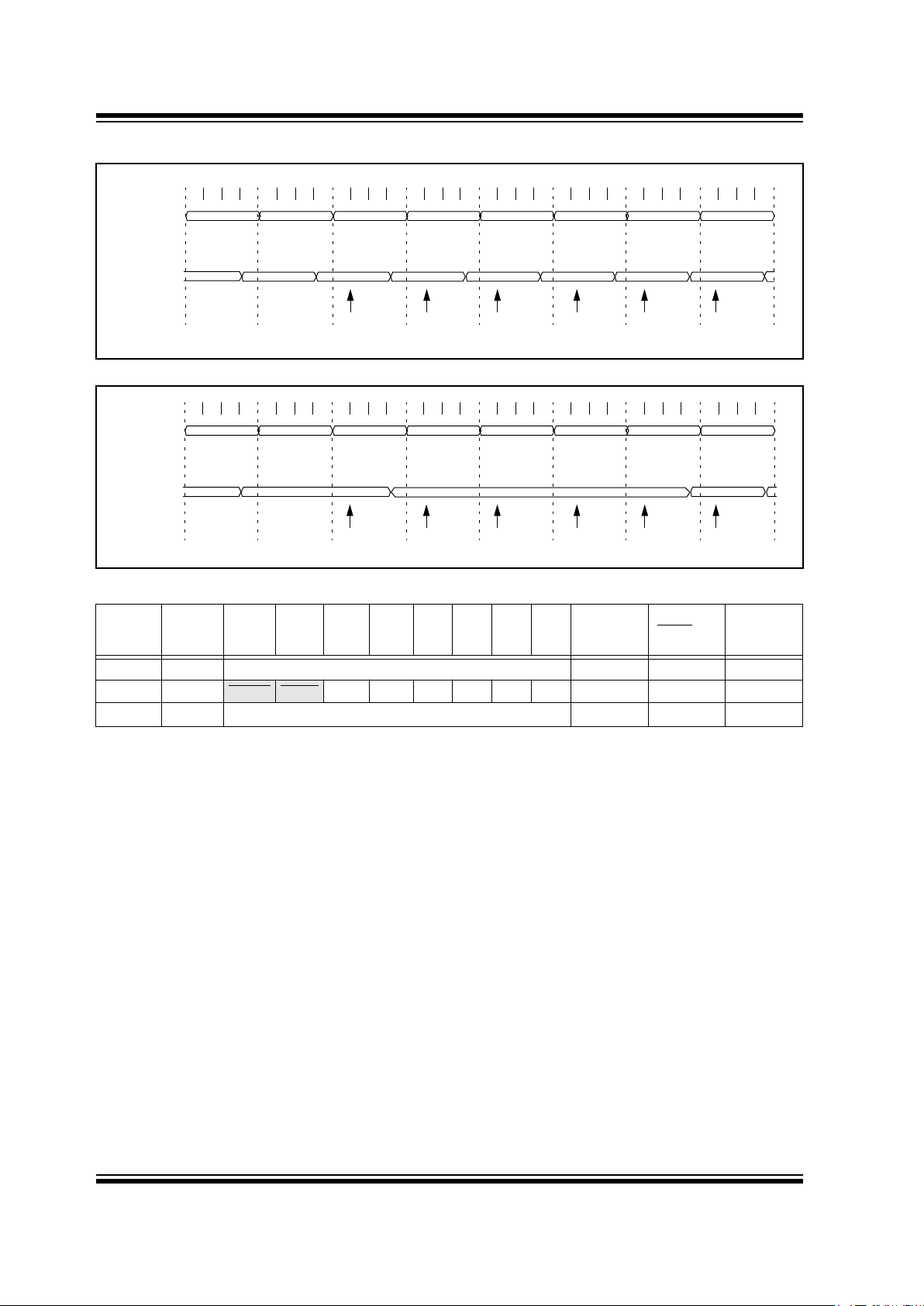
FIGURE 6-6: CURRENT ADDRESS READ
FIGURE 6-7: RANDOM READ
FIGURE 6-8: SEQUENTIAL READ
BUS ACTIVITY
MASTER
SDA LINE
BUS ACTIVITY
P
S
S
T
O
P
CONTROL
BYTE
S
T
A
R
T
DATA
A
C
K
N
O
A
C
K
1 10 0 X X X 1
X = Don’t Care Bit
P
BUS ACTIVITY
MASTER
SDA LINE
BUS ACTIVITY
S
T
A
R
T
S
T
O
P
CONTROL
BYTE
A
C
K
WORD
ADDRESS (n)
CONTROL
BYTE
S
T
A
R
T
DATA (n)
A
C
K
A
C
K
N
O
A
C
K
X X X X
S 1 10 0 X X X 0
S 1 10 0 X X X 1
X = Don’t Care Bit
P
BUS ACTIVITY
MASTER
SDA LINE
BUS ACTIVITY
S
T
O
P
CONTROL
BYTE
A
C
K
N
O
A
C
K
DATA n DATA n + 1 DATA n + 2 DATA n + X
A
C
K
A
C
K
A
C
K
12CF5XX_GEBook Page 24 Tuesday, October 21, 1997 8:23 AM
1997 Microchip Technology Inc. Preliminary DS40172A-page 25
PIC12CE5XX
7.0 TIMER0 MODULE AND
TMR0 REGISTER
The Timer0 module has the following features:
• 8-bit timer/counter register, TMR0
- Readable and writable
• 8-bit software programmable prescaler
• Internal or external clock select
- Edge select for external clock
Figure 7-1 is a simplified block diagram of the Timer0
module.
Timer mode is selected by clearing the T0CS bit
(OPTION<5>). In timer mode, the Timer0 module will
increment every instruction cycle (without prescaler). If
TMR0 register is written, the increment is inhibited for
the following two cycles (Figure 7-2 and Figure 7-3).
The user can work around this by writing an adjusted
value to the TMR0 register.
Counter mode is selected by setting the T0CS bit
(OPTION<5>). In this mode, Timer0 will increment
either on every rising or falling edge of pin T0CKI. The
T0SE bit (OPTION<4>) determines the source edge.
Clearing the T0SE bit selects the rising edge.
Restrictions on the external clock input are discussed
in detail in Section 7.1.
The prescaler may be used by either the Timer0
module or the Watchdog Timer, but not both. The
prescaler assignment is controlled in software by the
control bit PSA (OPTION<3>). Clearing the PSA bit
will assign the prescaler to Timer0. The prescaler is
not readable or writable. When the prescaler is
assigned to the Timer0 module, prescale v alues of 1:2,
1:4,..., 1:256 are selectable. Section 7.2 details the
operation of the prescaler.
A summary of registers associated with the Timer0
module is found in Table 7-1.
FIGURE 7-1: TIMER0 BLOCK DIAGRAM
Note 1: Bits T0CS, T0SE, PSA, PS2, PS1 and PS0 are located in the OPTION register.
2: The prescaler is shared with the Watchdog Timer (Figure 7-5).
0
1
1
0
T0CS
(1)
FOSC/4
Programmable
Prescaler
(2)
Sync with
Internal
Clocks
TMR0 reg
PSout
(2 cycle delay)
PSout
Data bus
8
PSA
(1)
PS2, PS1, PS0
(1)
3
Sync
T0SE
GP2/T0CKI
Pin
12CF5XX_GEBook Page 25 Tuesday, October 21, 1997 8:23 AM
PIC12CE5XX
DS40172A-page 26 Preliminary 1997 Microchip Technology Inc.
FIGURE 7-2: TIMER0 TIMING: INTERNAL CLOCK/NO PRESCALE
FIGURE 7-3: TIMER0 TIMING: INTERNAL CLOCK/PRESCALE 1:2
TABLE 7-1: REGISTERS ASSOCIATED WITH TIMER0
Address Name Bit 7 Bit 6 Bit 5 Bit 4 Bit 3 Bit 2 Bit 1 Bit 0
Value on
Power-On
Reset
Value on
MCLR and
WDT Reset
Value on
Wake-up on
Pin Change
01h TMR0 Timer0 - 8-bit real-time clock/counter xxxx xxxx uuuu uuuu
uuuu uuuu
N/A OPTION
GPWU GPPU T0CS T0SE PSA PS2 PS1 PS0 1111 1111 1111 1111
1111 1111
N/A TRIS I/O control registers --11 1111 --11 1111 --11 1111
Legend: Shaded cells not used by Timer0,
- = unimplemented, x = unknown, u = unchanged,
PC-1
Q1 Q2 Q3 Q4
Q1 Q2 Q3 Q4 Q1 Q2 Q3 Q4 Q1 Q2 Q3 Q4 Q1 Q2 Q3 Q4 Q1 Q2 Q3 Q4 Q1 Q2 Q3 Q4 Q1 Q2 Q3 Q4
PC
(Program
Counter)
Instruction
Fetch
Timer0
PC PC+1 PC+2 PC+3 PC+4 PC+5 PC+6
T0
T0+1 T0+2 NT0 NT0 NT0 NT0+1 NT0+2
MOVWF TMR0
MOVF TMR0,W MOVF TMR0,W MOVF TMR0,W MOVF TMR0,W MOVF TMR0,W
Write TMR0
executed
Read TMR0
reads NT0
Read TMR0
reads NT0
Read TMR0
reads NT0
Read TMR0
reads NT0 + 1
Read TMR0
reads NT0 + 2
Instruction
Executed
PC-1
Q1 Q2 Q3 Q4
Q1 Q2 Q3 Q4 Q1 Q2 Q3 Q4 Q1 Q2 Q3 Q4 Q1 Q2 Q3 Q4 Q1 Q2 Q3 Q4 Q1 Q2 Q3 Q4 Q1 Q2 Q3 Q4
PC
(Program
Counter)
Instruction
Fetch
Timer0
PC PC+1 PC+2 PC+3 PC+4 PC+5 PC+6
T0 NT0+1
MOVWF TMR0
MOVF TMR0,W MOVF TMR0,W MOVF TMR0,W MOVF TMR0,W MOVF TMR0,W
Write TMR0
executed
Read TMR0
reads NT0
Read TMR0
reads NT0
Read TMR0
reads NT0
Read TMR0
reads NT0
Read TMR0
reads NT0 + 1
T0+1
NT0
Instruction
Execute
T
0
12CF5XX_GEBook Page 26 Tuesday, October 21, 1997 8:23 AM
1997 Microchip Technology Inc. Preliminary DS40172A-page 27
PIC12CE5XX
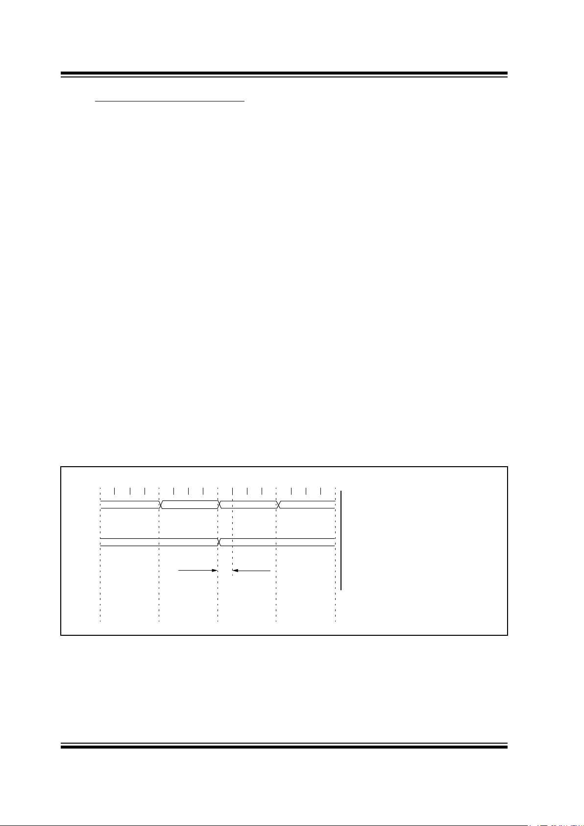
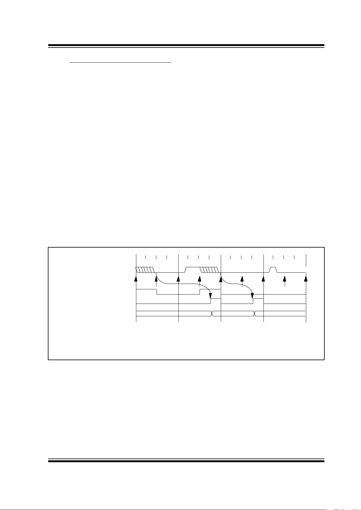
7.1 Using Timer0 with an External Clock
When an external clock input is used for Timer0, it
must meet certain requirements. The external clock
requirement is due to internal phase clock (T
OSC)
synchronization. Also, there is a delay in the actual
incrementing of Timer0 after synchronization.
7.1.1 EXTERNAL CLOCK SYNCHRONIZATION
When no prescaler is used, the external clock input is
the same as the prescaler output. The synchronization
of T0CKI with the internal phase clocks is
accomplished by sampling the prescaler output on the
Q2 and Q4 cycles of the internal phase clocks
(Figure 7-4). Therefore, it is necessary for T0CKI to be
high for at least 2T
OSC (and a small RC delay of 20 ns)
and low for at least 2T
OSC (and a small RC delay of
20 ns). Refer to the electrical specification of the
desired device.
When a prescaler is used, the external clock input is
divided by the asynchronous ripple counter-type
prescaler so that the prescaler output is symmetrical.
For the external clock to meet the sampling
requirement, the ripple counter must be taken into
account. Therefore, it is necessary for T0CKI to have a
period of at least 4T
OSC (and a small RC delay of
40 ns) divided by the prescaler value. The only
requirement on T0CKI high and low time is that they
do not violate the minimum pulse width requirement of
10 ns. Refer to parameters 40, 41 and 42 in the
electrical specification of the desired device.
7.1.2 TIMER0 INCREMENT DELAY
Since the prescaler output is synchronized with the
internal clocks, there is a small delay from the time the
external clock edge occurs to the time the Timer0
module is actually incremented. Figure 7-4 shows the
delay from the external clock edge to the timer
incrementing.
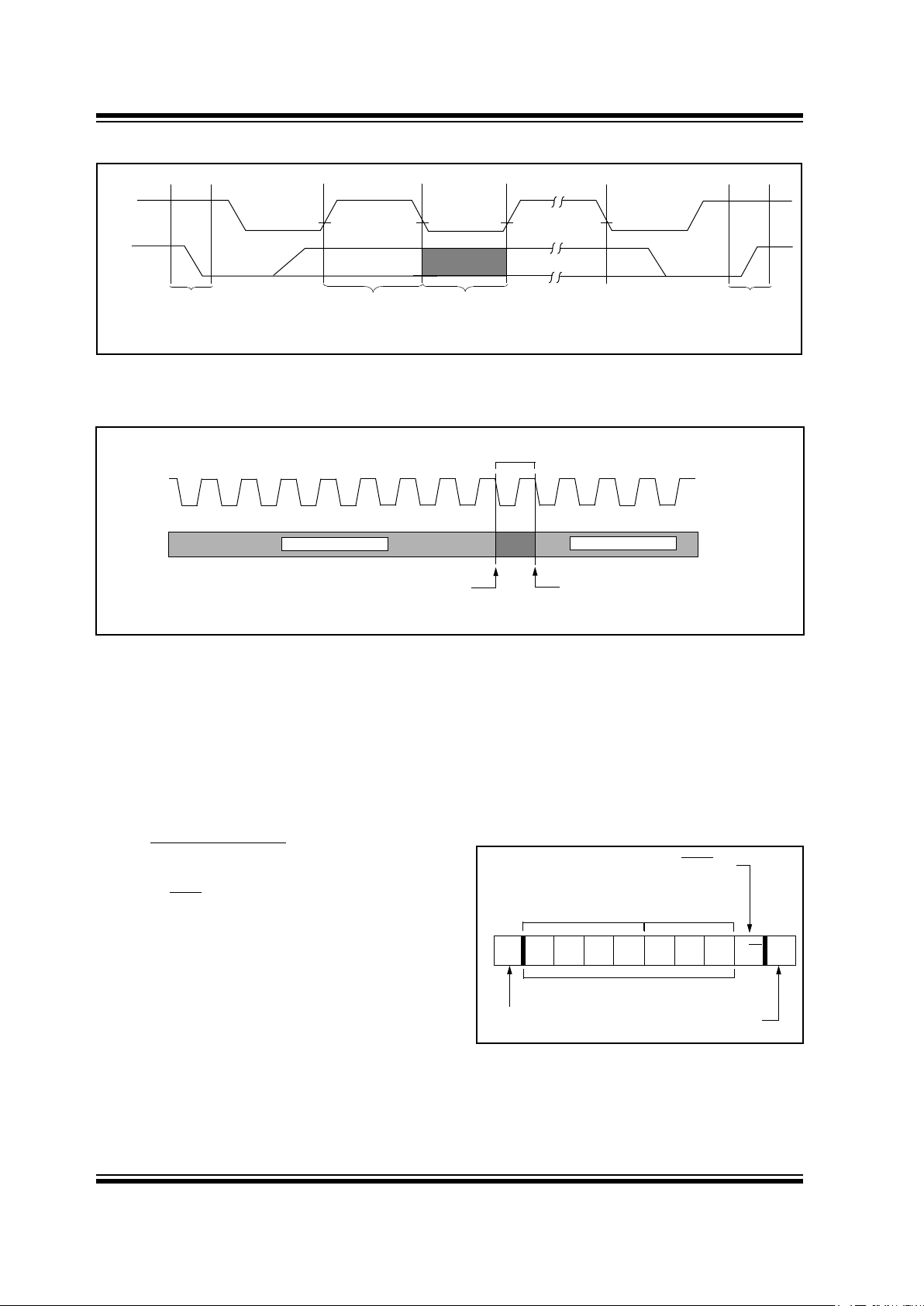
7.1.3 OPTION REGISTER EFFECT ON GP2 TRIS
If the option register is set to read TIMER0 from the pin,
the port is forced to an input regardless of the TRIS register setting.
FIGURE 7-4: TIMER0 TIMING WITH EXTERNAL CLOCK
Increment Timer0 (Q4)
External Clock Input or
Q1 Q2 Q3 Q4 Q1 Q2 Q3 Q4 Q1 Q2 Q3 Q4 Q1 Q2 Q3 Q4
Timer0
T0 T0 + 1 T0 + 2
Small pulse
misses sampling
External Clock/Prescaler
Output After Sampling
(3)
Note 1:
2:
3:
Delay from clock input change to Timer0 increment is 3Tosc to 7Tosc. (Duration of Q = Tosc).
Therefore, the error in measuring the interval between two edges on Timer0 input = ± 4Tosc max.
External clock if no prescaler selected, Prescaler output otherwise.
The arrows indicate the points in time where sampling occurs.
Prescaler Output (2)
(1)
12CF5XX_GEBook Page 27 Tuesday, October 21, 1997 8:23 AM

PIC12CE5XX
DS40172A-page 28 Preliminary 1997 Microchip Technology Inc.
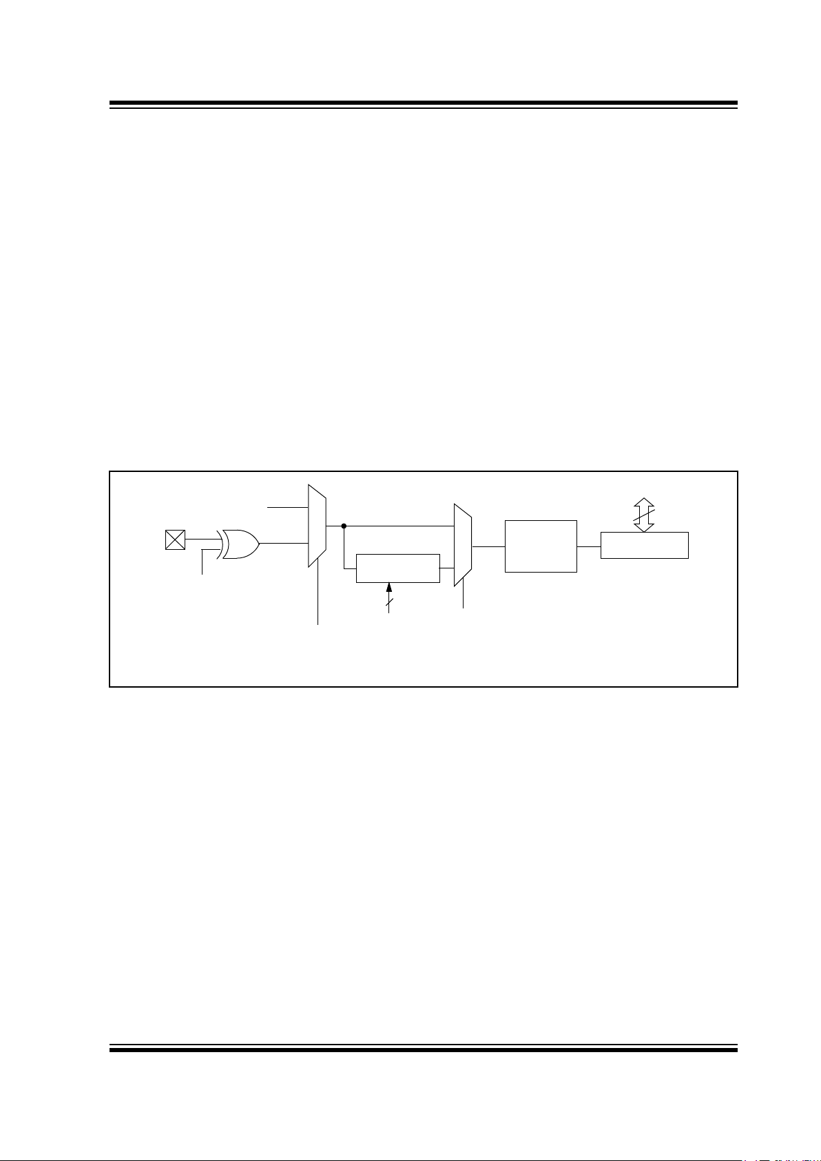
7.2 Prescaler
An 8-bit counter is available as a prescaler for the
Timer0 module, or as a postscaler for the Watchdog
Timer (WDT), respectively (Section 8.6). For simplicity,
this counter is being referred to as “prescaler”
throughout this data sheet. Note that the prescaler
may be used by either the Timer0 module or the WDT,
but not both. Thus, a prescaler assignment for the
Timer0 module means that there is no prescaler for
the WDT, and vice-versa.
The PSA and PS2:PS0 bits (OPTION<3:0>)
determine prescaler assignment and prescale ratio.
When assigned to the Timer0 module, all instructions
writing to the TMR0 register (e.g., CLRF 1, MOVWF 1,
BSF 1,x, etc.) will clear the prescaler. When assigned
to WDT, a CLRWDT instruction will clear the prescaler
along with the WDT. The prescaler is neither readable
nor writable. On a RESET, the prescaler contains all
'0's.
7.2.1 SWITCHING PRESCALER ASSIGNMENT
The prescaler assignment is fully under software control
(i.e., it can be changed “on the fly” during program
execution). To avoid an unintended device RESET, the
following instruction sequence (Example 7-1) must be
executed when changing the prescaler assignment from
Timer0 to the WDT.
EXAMPLE 7-1: CHANGING PRESCALER
(TIMER0→WDT)
1.CLRWDT ;Clear WDT
2.CLRF TMR0 ;Clear TMR0 & Prescaler
3.MOVLW '00xx1111’b;;These 3 lines (5, 6, 7)
4.OPTION ; are required only if
; desired
5.CLRWDT ;PS<2:0> are 000 or 001
6.MOVLW '00xx1xxx’b ;Set Postscaler to
7.OPTION ; desired WDT rate
To change prescaler from the WDT to the Timer0
module, use the sequence shown in Example 7-2. This
sequence must be used even if the WDT is disabled. A
CLRWDT instruction should be executed before s witching
the prescaler.
EXAMPLE 7-2: CHANGING PRESCALER
(WDT→TIMER0)
CLRWDT ;Clear WDT and
;prescaler
MOVLW 'xxxx0xxx' ;Select TMR0, new
;prescale value and
;clock source
OPTION
FIGURE 7-5: BLOCK DIAGRAM OF THE TIMER0/WDT PRESCALER
TCY ( = Fosc/4)
Sync
2
Cycles
TMR0 reg
8-bit Prescaler
8 - to - 1MUX
M
MUX
Watchdog
Timer
PSA
0
1
0
1
WDT
Time-Out
PS2:PS0
8
Note: T0CS, T0SE, PSA, PS2:PS0 are bits in the OPTION register.
PSA
WDT Enable bit
0
1
0
1
Data Bus
8
PSA
T0CS
M
U
X
M
U
X
U
X
T0SE
GP2/T0CKI
Pin
12CF5XX_GEBook Page 28 Tuesday, October 21, 1997 8:23 AM

1997 Microchip Technology Inc. Preliminary DS40172A-page 29
PIC12CE5XX
8.0 SPECIAL FEATURES OF THE
CPU
What sets a microcontroller apart from other
processors are special circuits to deal with the needs
of real-time applications. The PIC12CE5XX family of
microcontrollers has a host of such features intended
to maximize system reliability, minimize cost through
elimination of external components, provide power
saving operating modes and offer code protection.
These features are:
• Oscillator selection
• Reset
- Power-On Reset (POR)
- Device Reset Timer (DRT)
- Wake-up from SLEEP on pin change
• Watchdog Timer (WDT)
• SLEEP
• Code protection
• ID locations
• In-circuit Serial Programming
The PIC12CE5XX has a Watchdog Timer which can
be shut off only through configuration bit WDTE. It
runs off of its own RC oscillator for added reliability. If
using XT or LP selectable oscillator options, there is
always an 18 ms (nominal) delay provided by the
Device Reset Timer (DRT), intended to keep the chip
in reset until the crystal oscillator is stable. If using
INTRC or EXTRC there is an 18 ms delay only on V
DD
power-up. With this timer on-chip, most applications
need no external reset circuitry.
The SLEEP mode is designed to offer a very low
current power-down mode. The user can wake-up
from SLEEP through a change on input pins or
through a Watchdog Timer time-out. Several oscillator
options are also made available to allow the part to fit
the application, including an internal 4 MHz oscillator.
The EXTRC oscillator option saves system cost while
the LP crystal option saves power. A set of
configuration bits are used to select various options.
8.1 Configuration Bits
The PIC12CE5XX configuration word consists of 5
bits. Configuration bits can be programmed to select
various device configurations. Two bits are for the
selection of the oscillator type, one bit is the Watchdog
Timer enable bit, and one bit is the MCLR
enable bit.
One bit is the code protection bit (Figure 8-1).
FIGURE 8-1: CONFIGURATION WORD FOR PIC12CE5XX
— — — — — — — MCLRE CP WDTE FOSC1 FOSC0 Register: CONFIG
Address
(1)
: FFFh
bit11 10 9 8 7 6 5 4 3 2 1 bit0
bit 11-5: Unimplemented
bit 4: MCLRE: MCLR
enable bit.
1 = MCLR pin enabled
0 = MCLR tied to VDD, (Internally)
bit 3: CP: Code protection bit.
1 = Code protection off
0 = Code protection on
bit 2: WDTE: Watchdog timer enable bit
1 = WDT enabled
0 = WDT disabled
bit 1-0: FOSC1:FOSC0: Oscillator selection bits
11 = EXTRC - external RC oscillator
10 = INTRC - internal RC oscillator
01 = XT oscillator
00 = LP oscillator
Note 1: Refer to the PIC12C5XX Programming Specifications to determine how to access the
configuration word. This register is not user addressable during device operation. Refer to
In-Circuit Serial Programming™ Guide.
12CF5XX_GEBook Page 29 Tuesday, October 21, 1997 8:23 AM

PIC12CE5XX
DS40172A-page 30 Preliminary 1997 Microchip Technology Inc.
8.2 Oscillator Configurations
8.2.1 OSCILLATOR TYPES
The PIC12CE5XX can be operated in four different
oscillator modes. The user can program two
configuration bits (FOSC1:FOSC0) to select one of
these four modes:
• LP: Low Power Crystal
• XT: Crystal/Resonator
• INTRC: Internal 4 MHz Oscillator
• EXTRC: External Resistor/Capacitor
8.2.2 CRYSTAL OSCILLATOR / CERAMIC
RESONATORS
In XT or LP modes, a crystal or ceramic resonator is
connected to the GP5/OSC1/CLKIN and GP4/OSC2
pins to establish oscillation (Figure 8-2). The
PIC12CE5XX oscillator design requires the use of a
parallel cut crystal. Use of a series cut crystal may
give a frequency out of the crystal manufacturers
specifications. When in XT or LP modes, the device
can have an external clock source drive the GP5/
OSC1/CLKIN pin (Figure 8-3).
FIGURE 8-2: CRYSTAL OPERATION (OR
CERAMIC RESONATOR) (XT
OR LP OSC
CONFIGURATION)
FIGURE 8-3: EXTERNAL CLOCK INPUT
OPERATION (XT OR LP OSC
CONFIGURATION)
Note 1: See Capacitor Selection tables for
recommended values of C1 and C2.
2: A series resistor (RS) may be required for
AT strip cut crystals.
3: RF varies with the crystal chosen
(approx. value = 10 MΩ).
C1
(1)
C2
(1)
XTAL
OSC2
OSC1
RF
(3)
SLEEP
To internal
logic
RS
(2)
PIC12CE5XX
Clock from
ext. system
OSC1
OSC2
PIC12CE5XX
Open
TABLE 8-1: CAPACITOR SELECTION
FOR CERAMIC RESONATORS
- PIC12CE5XX
T ABLE 8-2: CAPACITOR SELECTION
FOR CRYSTAL OSCILLATOR
- PIC12CE5XX
Osc
Type
Resonator
Freq
Cap. RangeC1Cap. Range
C2
XT 4.0 MHz 30 pF 30 pF
These values are for design guidance only. Since
each resonator has its own characteristics, the user
should consult the resonator manufacturer for
appropriate values of external components.
Osc
Type
Resonator
Freq
Cap.Range
C1
Cap. Range
C2
LP 32 kHz
(1)
15 pF 15 pF
XT 200 kHz
1 MHz
4 MHz
47-68 pF
15 pF
15 pF
47-68 pF
15 pF
15 pF
Note 1: For V
DD > 4.5V, C1 = C2 ≈ 30 pF is
recommended.
These values are for design guidance only. Rs may
be required in XT mode to avoid overdriving crystals
with low drive level specification. Since each crystal
has its own characteristics, the user should consult
the crystal manufacturer for appropriate values of
external components.
12CF5XX_GEBook Page 30 Tuesday, October 21, 1997 8:23 AM

1997 Microchip Technology Inc. Preliminary DS40172A-page 31
PIC12CE5XX
8.2.3 EXTERNAL CRYSTAL OSCILLATOR
CIRCUIT
Either a prepackaged oscillator or a simple oscillator
circuit with TTL gates can be used as an external
crystal oscillator circuit. Prepackaged oscillators
provide a wide operating range and better stability. A
well-designed crystal oscillator will provide good
performance with TTL gates. Two types of crystal
oscillator circuits can be used: one with parallel
resonance, or one with series resonance.
Figure 8-4 shows implementation of a parallel
resonant oscillator circuit. The circuit is designed to
use the fundamental frequency of the crystal. The
74AS04 inverter performs the 180-degree phase shift
that a parallel oscillator requires. The 4.7 kΩ resistor
provides the negative feedback for stability. The 10 kΩ
potentiometers bias the 74AS04 in the linear region.
This circuit could be used for external oscillator
designs.
FIGURE 8-4: EXTERNAL PARALLEL
RESONANT CRYSTAL
OSCILLATOR CIRCUIT
Figure 8-5 shows a series resonant oscillator circuit.
This circuit is also designed to use the fundamental
frequency of the crystal. The inverter performs a 180degree phase shift in a series resonant oscillator
circuit. The 330 Ω resistors provide the negative
feedback to bias the inverters in their linear region.
FIGURE 8-5: EXTERNAL SERIES
RESONANT CRYSTAL
OSCILLATOR CIRCUIT
20 pF
+5V
20 pF
10k
4.7k
10k
74AS04
XTAL
10k
74AS04
PIC12CE5XX
CLKIN
To Other
Devices
330
74AS04
74AS04
PIC12CE5X
X
CLKIN
To Other
Devices
XTAL
330
74AS04
0.1 µF
8.2.4 EXTERNAL RC OSCILLATOR
For timing insensitive applications, the RC device
option offers additional cost savings. The RC oscillator
frequency is a function of the supply voltage, the
resistor (Rext) and capacitor (Cext) values, and the
operating temperature. In addition to this, the oscillator
frequency will vary from unit to unit due to normal
process parameter variation. Furthermore, the
difference in lead frame capacitance between package
types will also affect the oscillation frequency,
especially for low Cext values. The user also needs to
take into account variation due to tolerance of external
R and C components used.
Figure 8-6 shows how the R/C combination is
connected to the PIC12CE5XX. For Rext values below
2.2 kΩ, the oscillator operation may become unstable,
or stop completely. For very high Rext values
(e.g., 1 MΩ) the oscillator becomes sensitive to noise,
humidity and leakage. Thus, we recommend keeping
Rext between 3 kΩ and 100 kΩ.
Although the oscillator will operate with no external
capacitor (Cext = 0 pF), we recommend using values
above 20 pF for noise and stability reasons. With no or
small external capacitance, the oscillation frequency
can vary dramatically due to changes in external
capacitances, such as PCB trace capacitance or
package lead frame capacitance.
The Electrical Specifications sections show RC
frequency variation from part to part due to normal
process variation. The variation is larger for larger R
(since leakage current variation will affect RC
frequency more for large R) and for smaller C (since
variation of input capacitance will affect RC frequency
more).
Also, see the Electrical Specifications sections for
variation of oscillator frequency due to V
DD for given
Rext/Cext values as well as frequency variation due to
operating temperature for given R, C, and V
DD values.
FIGURE 8-6: EXTERNAL RC OSCILLATOR
MODE
VDD
Rext
Cext
V
SS
OSC1
Internal
clock
PIC12CE5XX
N
12CF5XX_GEBook Page 31 Tuesday, October 21, 1997 8:23 AM

PIC12CE5XX
DS40172A-page 32 Preliminary 1997 Microchip Technology Inc.
8.2.5 INTERNAL 4 MHz RC OSCILLATOR
The internal RC oscillator provides a fixed 4 MHz (nom-
inal) system clock at VDD = 5V and 25°C, see “Electrical Specifications” section for information on variation
over voltage and temperature..
In addition, a calibration instruction is programmed into
the top of memory which contains the calibration value
for the internal RC oscillator. This value is prog rammed
as a MOVLW XX instruction where XX is the calibration
value, and is placed at the reset vector. This will load
the W register with the calibration value upon reset and
the PC will then roll over to the users program at
address 0x000. The user then has the option of writing
the value to the OSCCAL Register (05h) or ignoring it.
OSCCAL, when written to with the calibration value, will
“trim” the internal oscillator to remove process variation
from the oscillator frequency. .
For the PIC12CE518 and PIC12CE519, bits <7:4>,
CAL3-CAL0 are used for fine calibration while bit 3,
CALFST, and bit 2,CALSLW are used for more coarse
adjustment. Adjusting CAL3-0 from 0000 to 1111
yields a higher clock speed. Set CALFST = 1 for
greater increase in frequency or set CALSLW = 1 for
greater decrease in frequency. Note that bits 1 and 0
of OSCCAL are unimplemented and should be written
as 0 when modifying OSCALL for compatibility with
future devices.
For the PIC12CE518 and PIC12CE519, the upper 4
bits of the register are used to allow for future, longer bit
length calibration schemes. Writing a larger value in
this location yields a higher clock speed.
8.3 RESET
The device differentiates between various kinds of
reset:
a) Power on reset (POR)
b) MCLR
reset during normal operation
c) MCLR
reset during SLEEP
d) WDT time-out reset during normal operation
e) WDT time-out reset during SLEEP
f) Wake-up from SLEEP on pin change
Some registers are not reset in any way; they are
unknown on POR and unchanged in any other reset.
Most other registers are reset to “reset state” on po weron reset (POR), on MCLR
, WDT or wake-up on pin
change reset during normal operation. They are not
affected by a WDT reset during SLEEP or MCLR
reset
during SLEEP, since these resets are viewed as
Note: Please note that erasing the device will
also erase the pre-programmed internal
calibration value for the inter nal oscillator.
The calibration value must be saved prior
to erasing the part.
resumption of normal operation. The exceptions to this
are T
O, PD, and GPWUF bits. They are set or cleared
differently in different reset situations. These bits are
used in software to determine the nature of reset. See
Table 8-3 for a full description of reset states of all
registers.
12CF5XX_GEBook Page 32 Tuesday, October 21, 1997 8:23 AM

1997 Microchip Technology Inc. Preliminary DS40172A-page 33
PIC12CE5XX
TABLE 8-3: RESET CONDITIONS FOR REGISTERS
TABLE 8-4: RESET CONDITION FOR SPECIAL REGISTERS
Register Address Power-on Reset
MCLR
Reset
WDT time-out
Wake-up on Pin Change
W — qqqq xxxx (1) qqqq uuuu (1)
INDF 00h xxxx xxxx uuuu uuuu
TMR0 01h xxxx xxxx uuuu uuuu
PC 02h 1111 1111 1111 1111
STATUS 03h 0001 1xxx ?00? ?uuu (2)
FSR (12CF518) 04h 111x xxxx 111u uuuu
FSR (12CF519) 04h 110x xxxx 11uu uuuu
OSCCAL 05h 0111 00-- uuuu uu--
GPIO 06h 11xx xxxx 11uu uuuu
OPTION — 1111 1111 1111 1111
TRIS — --11 1111 --11 1111
Legend: u = unchanged, x = unknown, - = unimplemented bit, read as ‘0’, ? = value depends on condition.
Note 1: Bits <7:4> of W register contain oscillator calibration values due to MOVLW XX instruction at top of memory.
Note 2: See Table 8-7 for reset value for specific conditions
STATUS Addr: 03h PCL Addr: 02h
Power on reset 0001 1xxx 1111 1111
MCLR
reset during normal operation 000u uuuu 1111 1111
MCLR
reset during SLEEP 0001 0uuuu 1111 1111
WDT reset during SLEEP 0000 0uuu 1111 1111
WDT reset normal operation 0000 1uuu 1111 1111
Wake-up from SLEEP on pin change 1001 0uuu 1111 1111
Legend: u = unchanged, x = unknown, - = unimplemented bit, read as ‘0’.
12CF5XX_GEBook Page 33 Tuesday, October 21, 1997 8:23 AM

PIC12CE5XX
DS40172A-page 34 Preliminary 1997 Microchip Technology Inc.
8.3.1 MCLR ENABLE
This configuration bit when unprogrammed (left in the
‘1’ state) enables the external MCLR
function. When
programmed, the MCLR
function is tied to the internal
V
DD, and the pin is assigned to be a GPIO. See
Figure 8-7.
FIGURE 8-7: MCLR SELECT
8.4 P
ower-On Reset (POR)
The PIC12CE5XX family incorporates on-chip PowerOn Reset (POR) circuitry which provides an internal
chip reset for most power-up situations.
A Power-on Reset pulse is generated on-chip when
V
DD rise is detected (in the range of 1.5V - 2.1V). To
take advantage of the internal POR, program the GP3/
MCLR
/VPP pin as MCLR and tie directly to VDD or program the pin as GP3. An internal weak pull-up resistor
is implemented using a transistor. Refer to Table 11-7
for the pull-up resistor ranges. This will eliminate external RC components usually needed to create a Poweron Reset. A maximum rise time for V
DD is specified.
See Electrical Specifications for details.
When the device starts normal operation (exits the
reset condition), device operating parameters (voltage ,
frequency, temperature, ...) must be met to ensure
operation. If these conditions are not met, the device
must be held in reset until the operating parameters are
met.
A simplified block diagram of the on-chip Power-On
Reset circuit is shown in Figure 8-8.
GP3/MCLR/VPP
MCLRE
INTERNAL MCLR
WEAK
PULL-UP
The Power-On Reset circuit and the Device Reset
Timer (Section 8.5) circuit are closely related. On
power-up, the reset latch is set and the DRT is reset.
The DRT timer begins counting once it detects MCLR
to be high. After the time-out period, which is typically
18 ms, it will reset the reset latch and thus end the onchip reset signal.
A power-up example where MCLR
is held low is
shown in Figure 8-9. V
DD is allowed to rise and
stabilize before bringing MCLR
high. The chip will
actually come out of reset T
DRT msec after MCLR
goes high.
In Figure 8-10, the on-chip Power-On Reset feature is
being used (MCLR
and VDD are tied together or the
pin is programmed to be GP3.). The V
DD is stable
before the start-up timer times out and there is no
problem in getting a proper reset. However, Figure 811 depicts a problem situation where V
DD rises too
slowly. The time between when the DRT senses that
MCLR
is high and when MCLR (and VDD) actually
reach their full value, is too long. In this situation, when
the start-up timer times out, V
DD has not reached the
V
DD (min) value and the chip is, therefore, not
guaranteed to function correctly. For such situations,
we recommend that external RC circuits be used to
achieve longer POR delay times (Figure 8-10).
For additional information refer to Application Notes
“
Power-Up Considerations”
- AN522 and “
Power-up
Trouble Shooting
” - AN607.
Note: When the device starts normal operation
(exits the reset condition), device operating parameters (voltage, frequency, temperature, etc.) must be meet to ensure
operation. If these conditions are not met,
the device must be held in reset until the
operating conditions are met.
12CF5XX_GEBook Page 34 Tuesday, October 21, 1997 8:23 AM

1997 Microchip Technology Inc. Preliminary DS40172A-page 35
PIC12CE5XX
FIGURE 8-8: SIMPLIFIED BLOCK DIAGRAM OF ON-CHIP RESET CIRCUIT
FIGURE 8-9: TIME-OUT SEQUENCE ON POWER-UP (MCLR
PULLED LOW)
FIGURE 8-10: TIME-OUT SEQUENCE ON POWER-UP (MCLR
TIED TO VDD): FAST VDD RISE TIME
S Q
R
Q
VDD
GP3/MCLR/VPP
Power-Up
Detect
On-Chip
DRT OSC
POR (Power-On Reset)
WDT Time-out
RESET
CHIP RESET
8-bit Asynch
Ripple Counter
(Start-Up Timer)
MCLRE
SLEEP
Pin Change
Wake-up on
pin change
VDD
MCLR
INTERNAL POR
DRT TIME-OUT
INTERNAL RESET
TDRT
VDD
MCLR
INTERNAL POR
DRT TIME-OUT
INTERNAL RESET
TDRT
12CF5XX_GEBook Page 35 Tuesday, October 21, 1997 8:23 AM

PIC12CE5XX
DS40172A-page 36 Preliminary 1997 Microchip Technology Inc.
FIGURE 8-11: TIME-OUT SEQUENCE ON POWER-UP (MCLR TIED TO VDD): SLO W VDD RISE TIME
VDD
MCLR
INTERNAL POR
DRT TIME-OUT
INTERNAL RESET
TDRT
V1
When VDD rises slowly, the TDRT time-out expires long before VDD has reached its final value. In
this example, the chip will reset properly if, and only if, V1 ≥ VDD min.
8.5 Device Reset Timer (DRT)
In the PIC12CE5XX, the DRT runs any time the device
is powered up. DRT runs from RESET and varies
based on oscillator selection (see Table 8-5.)
The Device Reset Timer (DRT) provides a fixed 18 ms
nominal time-out on reset. The DRT operates on an
internal RC oscillator. The processor is kept in RESET
as long as the DRT is active. The DRT delay allows
V
DD to rise above VDD min., and for the oscillator to
stabilize.
Oscillator circuits based on crystals or ceramic
resonators require a certain time after power-up to
establish a stable oscillation. The on-chip DRT keeps
the device in a RESET condition for approximately 18
ms after MCLR
has reached a logic high level. Thus,
programming GP3/MCLR
/VPP as MCLR and using an
external RC network connected to the MCLR
input is
not required in most cases, allowing for savings in
cost-sensitive and/or space restricted applications, as
well as allowing the use of the GP3/MCLR
/VPP pin as
a general purpose input.
The Device Reset time delay will v ary from chip to chip
due to V
DD, temperature, and process variation. See
AC parameters for details.
The DRT will also be triggered upon a W atchdog Timer
time-out (only in XT and LP modes). This is
particularly impor tant for applications using the WDT
to wake from SLEEP mode automatically.
TABLE 8-5: DRT (DEVICE RESET TIMER
PERIOD)
8.6 Watchdog Timer (WDT)
The Watchdog Timer (WDT) is a free running on-chip
RC oscillator which does not require any external
components. This RC oscillator is separate from the
external RC oscillator of the GP5/OSC1/CLKIN pin
and the internal 4 MHz oscillator. That means that the
WDT will run even if the main processor clock has
been stopped, for example, by execution of a SLEEP
instruction. During normal operation or SLEEP, a WDT
reset or wake-up reset generates a device RESET.
The T
O bit (STATUS<4>) will be cleared upon a
Watchdog Timer reset.
The WDT can be permanently disabled by
programming the configuration bit WDTE as a '0'
(Section 8.1). Refer to the PIC12CE5XX Programming
Specifications to determine how to access the
configuration word.
Oscillator
Configuration
POR Reset
Subsequent
Resets
IntRC &
ExtRC
18 ms (typical) 300 µs
(typical)
XT & LP 18 ms (typical) 18 ms (typical)
12CF5XX_GEBook Page 36 Tuesday, October 21, 1997 8:23 AM

1997 Microchip Technology Inc. Preliminary DS40172A-page 37
PIC12CE5XX
8.6.1 WDT PERIOD
The WDT has a nominal time-out period of 18 ms,
(with no prescaler). If a longer time-out period is
desired, a prescaler with a division ratio of up to 1:128
can be assigned to the WDT (under software control)
by writing to the OPTION register. Thus, a time-out
period of a nominal 2.3 seconds can be realized.
These periods vary with temperature, V
DD and part-to-
part process variations (see DC specs).
Under worst case conditions (V
DD = Min., Temperature
= Max., max. WDT prescaler), it may take several
seconds before a WDT time-out occurs.
8.6.2 WDT PROGRAMMING CONSIDERATIONS
The CLRWDT instruction clears the WDT and the
postscaler, if assigned to the WDT, and prevents it
from timing out and generating a device RESET.
The SLEEP instruction resets the WDT and the
postscaler, if assigned to the WDT. This gives the
maximum SLEEP time before a WDT wake-up reset.
FIGURE 8-12: WATCHDOG TIMER BLOCK DIAGRAM
TABLE 8-6: SUMMARY OF REGISTERS ASSOCIATED WITH THE WATCHDOG TIMER
Address Name Bit 7 Bit 6 Bit 5 Bit 4 Bit 3 Bit 2 Bit 1 Bit 0
Value on
Power-On
Reset
Value on
MCLR and
WDT Reset
Value on
Wake-up on
Pin Change
N/A OPTION GPWU GPPU T0CS T0SE PSA PS2 PS1 PS0 1111 1111 1111 1111
1111 1111
Legend: Shaded boxes = Not used by Watchdog Timer, — = unimplemented, read as '0', u = unchanged
1
0
1
0
From Timer0 Clock Source
(Figure 7-5)
To Timer0 (Figure 7-4)
Postscaler
WDT Enable
Configuration Bit
PSA
WDT
Time-out
PS2:PS0
PSA
MUX
8 - to - 1 MUX
Postscaler
M
U
X
Watchdog
Timer
Note: T0CS, T0SE, PSA, PS2:PS0
are bits in the OPTION register.
12CF5XX_GEBook Page 37 Tuesday, October 21, 1997 8:23 AM

PIC12CE5XX
DS40172A-page 38 Preliminary 1997 Microchip Technology Inc.
8.7 Time-Out Sequence, Power Down,
and Wake-up from SLEEP Status Bits
(TO/PD/GPWUF)
The TO, PD, and GPWUF bits in the STATUS register
can be tested to determine if a RESET condition has
been caused by a power-up condition, a MCLR
or
Watchdog Timer (WDT) reset, or a MCLR
or WDT
reset.
These STATUS bits are only affected by events listed
in Table 8-8.
Table 8-4 lists the reset conditions for the special
function registers, while Table 8-3 lists the reset
conditions for all the registers.
TABLE 8-7: TO/PD/GPWUF STATUS
AFTER RESET
GPWUF TO PD RESET caused by
0 0 0
WDT wake-up from
SLEEP
0 0 1
WDT time-out (not from
SLEEP)
0 1 0
MCLR wake-up from
SLEEP
0 1 1
Power-up
0 u u
MCLR not during SLEEP
1 1 0
Wake-up from SLEEP on
pin change
Legend: Legend: u = unchanged
Note 1: The TO, PD, and GPWUF bits main-
tain their status (u) until a reset
occurs. A low-pulse on the MCLR
input does not change the TO, PD,
and GPWUF status bits.
TABLE 8-8: EVENTS AFFECTING TO/PD
STATUS BITS
Event GPWUF TO PD Remarks
Power-up
0 1 1
WDT Time-out
0 0 u
No effect
on PD
SLEEP instruction
u 1 0
CLRWDT
instruction
u 1 1
Wake-up from
SLEEP on pin
change
1 1 0
Legend: u = unchanged
A WDT time-out will occur regardless of the status of the
TO bit. A SLEEP instruction will be executed, regardless of
the status of the PD bit. Table 8-7 reflects the status of TO
and PD after the corresponding event.
8.8 Reset on Brown-Out
A brown-out is a condition where device power (VDD)
dips below its minimum value, b ut not to z ero , and then
recovers. The device should be reset in the event of a
brown-out.
To reset PIC12CE5XX devices when a brown-out
occurs, external brown-out protection circuits may be
built, as shown in Figure 8-13 and Figure 8-14.
FIGURE 8-13: BROWN-OUT PROTECTION
CIRCUIT 1
FIGURE 8-14: BROWN-OUT PROTECTION
CIRCUIT 2
This circuit will activate reset when VDD goes below Vz +
0.7V (where Vz = Zener voltage).
*Refer to Figure 8-7 and Table 11-7 for internal weak pull-
up on MCLR.
33k
10k
40k*
V
DD
MCLR
PIC12CE5XX
VDD
Q1
This brown-out circuit is less expensive, although
less accurate. Transistor Q1 turns off when V
DD
is below a certain level such that:
*Refer to Figure 8-7 and Table 11-7 for internal weak
pull-up on MCLR.
VDD •
R1
R1 + R2
= 0.7V
R2
40k
V
DD
MCLR
PIC12CE5XX
R1
Q1
VDD
12CF5XX_GEBook Page 38 Tuesday, October 21, 1997 8:23 AM

1997 Microchip Technology Inc. Preliminary DS40172A-page 39
PIC12CE5XX
8.9 Power-Down Mode (SLEEP)
A device may be powered down (SLEEP) and later
powered up (Wake-up from SLEEP).
8.9.1 SLEEP
The Power-Down mode is entered by executing a
SLEEP instruction.
If enabled, the Watchdog Timer will be cleared but
keeps running, the T
O bit (STATUS<4>) is set, the PD
bit (STATUS<3>) is cleared and the oscillator driver is
turned off. The I/O ports maintain the status they had
before the SLEEP instruction was executed (driving
high, driving low, or hi-impedance).
It should be noted that a RESET generated by a WDT
time-out does not drive the MCLR
pin low.
For lowest current consumption while powered down,
the T0CKI input should be at V
DD or VSS and the GP3/
MCLR
/VPP pin must be at a logic high level if MCLR is
enabled.
8.9.2 WAKE-UP FROM SLEEP
The device can wake-up from SLEEP through one of
the following events:
1. An external reset input on GP3/MCLR
/VPP pin,
when configured as MCLR
.
2. A Watchdog Timer time-out reset (if WDT was
enabled).
3. A change on input pin GP0, GP1, or GP3/
MCLR
/VPP when wake-up on change is
enabled.
These events cause a device reset. The T
O, PD, and
GPWUF bits can be used to determine the cause of
device reset. The T
O bit is cleared if a WDT time-out
occurred (and caused wake-up). The PD
bit, which is
set on power-up, is cleared when SLEEP is invoked.
The GPWUF bit indicates a change in state while in
SLEEP at pins GP0, GP1, or GP3 (since the last time
there was a file or bit operation on GP port).
The WDT is cleared when the device wakes from
sleep, regardless of the wake-up source.
Caution: Right before entering SLEEP, read the
input pins. When in SLEEP, wake up
occurs when the values at the pins change
from the state they were in at the last
reading. If a wake-up on change occurs
and the pins are not read before
reentering SLEEP, a wake up will occur
immediately even if no pins change while
in SLEEP mode.
8.10 Program Verification/Code Protection
If the code protection bit has not been programmed,
the on-chip program memory can be read out for
verification purposes.
The first 64 locations can be read regardless of the
code protection bit setting.
Note: The location containing the pre-pro-
grammed internal RC oscillator calibration
value is never code protected.
8.11 ID Locations
Four memory locations are designated as ID locations
where the user can store checksum or other codeidentification numbers. These locations are not
accessible during normal execution but are readable
and writable during program/verify.
Use only the lower 4 bits of the ID locations and
always program the upper 8 bits as '0's.
12CF5XX_GEBook Page 39 Tuesday, October 21, 1997 8:23 AM

PIC12CE5XX
DS40172A-page 40 Preliminary 1997 Microchip Technology Inc.
8.12 In-Circuit Serial Programming™
The PIC12CE5XX microcontrollers program memory
can be serially programmed while in the end application circuit. This is simply done with two lines for clock
and data, and three other lines for power, ground, and
the programming voltage. This allows customers to
manufacture boards with unprogrammed devices, and
then program the microcontroller just before shipping
the product. This also allows the most recent firmware
or a custom firmware to be programmed.
The device is placed into a program/verify mode by
holding the GP1 and GP0 pins low while raising the
MCLR
(VPP) pin from VIL to VIHH (see programming
specification). GP1 becomes the programming clock
and GP0 becomes the programming data. Both GP1
and GP0 are Schmitt Trigger inputs in this mode.
After reset, a 6-bit command is then supplied to the
device. Depending on the command, 14-bits of program data are then supplied to or from the device,
depending if the command was a load or a read. For
complete details of serial programming, please refer to
the PIC12CE5XX Programming Specifications in the
In-Circuit Serial Programming Guide.
A typical in-circuit serial programming connection is
shown in Figure 8-15.
FIGURE 8-15: TYPICAL IN-CIRCUIT SERIAL
PROGRAMMING
CONNECTION
External
Connector
Signals
To Normal
Connections
To Normal
Connections
PIC12CE5XX
V
DD
VSS
MCLR/VPP
GP1
GP0
+5V
0V
VPP
CLK
Data I/O
V
DD
12CF5XX_GEBook Page 40 Tuesday, October 21, 1997 8:23 AM

1997 Microchip Technology Inc. Preliminary DS40172A-page 41
PIC12CE5XX
9.0 INSTRUCTION SET SUMMARY
Each PIC12CE5XX instruction is a 12-bit word divided
into an OPCODE, which specifies the instruction type,
and one or more operands which further specify the
operation of the instruction. The PIC12CE5XX
instruction set summary in Table 9-2 groups the
instructions into byte-oriented, bit-oriented, and literal
and control operations. Table 9-1 shows the opcode
field descriptions.
For byte-oriented instructions, 'f' represents a file
register designator and 'd' represents a destination
designator. The file register designator is used to
specify which one of the 32 file registers is to be used
by the instruction.
The destination designator specifies where the result
of the operation is to be placed. If 'd' is '0', the result is
placed in the W register. If 'd' is '1', the result is placed
in the file register specified in the instruction.
For bit-oriented instructions, 'b' represents a bit field
designator which selects the number of the bit affected
by the operation, while 'f' represents the number of the
file in which the bit is located.
For literal and control operations, 'k' represents an
8 or 9-bit constant or literal value.
TABLE 9-1: OPCODE FIELD
DESCRIPTIONS
Field Description
f Register file address (0x00 to 0x7F)
W Working register (accumulator)
b Bit address within an 8-bit file register
k Literal field, constant data or label
x
Don't care location (= 0 or 1)
The assembler will generate code with x = 0. It is
the recommended form of use for compatibility
with all Microchip software tools.
d
Destination select;
d = 0 (store result in W)
d = 1 (store result in file register 'f')
Default is d = 1
label Label name
TOS Top of Stack
PC Program Counter
WDT Watchdog Timer Counter
TO
Time-Out bit
PD Power-Down bit
dest
Destination, either the W register or the specified
register file location
[ ]
Options
( )
Contents
→
Assigned to
< >
Register bit field
∈
In the set of
i
talics
User defined term (font is courier)
All instructions are executed within a single instruction
cycle, unless a conditional test is true or the program
counter is changed as a result of an instruction. In this
case, the execution takes two instruction cycles. One
instruction cycle consists of four oscillator periods.
Thus, for an oscillator frequency of 4 MHz, the normal
instruction execution time is 1 µs. If a conditional test
is true or the program counter is changed as a result of
an instruction, the instruction execution time is 2 µs.
Figure 9-1 shows the three general formats that the
instructions can have. All examples in the figure use the
following format to represent a hexadecimal number:
0xhhh
where 'h' signifies a hexadecimal digit.
FIGURE 9-1: GENERAL FORMAT FOR
INSTRUCTIONS
Byte-oriented file register operations
11 6 5 4 0
d = 0 for destination W
OPCODE d f (FILE #)
d = 1 for destination f
f = 5-bit file register address
Bit-oriented file register operations
11 8 7 5 4 0
OPCODE b (BIT #) f (FILE #)
b = 3-bit bit address
f = 5-bit file register address
Literal and control operations (except GOTO)
11 8 7 0
OPCODE k (literal)
k = 8-bit immediate value
Literal and control operations - GOTO instruction
11 9 8 0
OPCODE k (literal)
k = 9-bit immediate value
12CF5XX_GEBook Page 41 Tuesday, October 21, 1997 8:23 AM

PIC12CE5XX
DS40172A-page 42 Preliminary 1997 Microchip Technology Inc.
TABLE 9-2: INSTRUCTION SET SUMMARY
Mnemonic,
Operands Description Cycles
12-Bit Opcode
Status
Affected NotesMSb LSb
ADDWF
ANDWF
CLRF
CLRW
COMF
DECF
DECFSZ
INCF
INCFSZ
IORWF
MOVF
MOVWF
NOP
RLF
RRF
SUBWF
SWAPF
XORWF
f,d
f,d
f
–
f, d
f, d
f, d
f, d
f, d
f, d
f, d
f
–
f, d
f, d
f, d
f, d
f, d
Add W and f
AND W with f
Clear f
Clear W
Complement f
Decrement f
Decrement f, Skip if 0
Increment f
Increment f, Skip if 0
Inclusive OR W with f
Move f
Move W to f
No Operation
Rotate left f through Carry
Rotate right f through Carry
Subtract W from f
Swap f
Exclusive OR W with f
1
1
1
1
1
1
1(2)
1
1(2)
1
1
1
1
1
1
1
1
1
0001
0001
0000
0000
0010
0000
0010
0010
0011
0001
0010
0000
0000
0011
0011
0000
0011
0001
11df
01df
011f
0100
01df
11df
11df
10df
11df
00df
00df
001f
0000
01df
00df
10df
10df
10df
ffff
ffff
ffff
0000
ffff
ffff
ffff
ffff
ffff
ffff
ffff
ffff
0000
ffff
ffff
ffff
ffff
ffff
C,DC,Z
Z
Z
Z
Z
Z
None
Z
None
Z
Z
None
None
C
C
C,DC,Z
None
Z
1,2,4
2,4
4
2,4
2,4
2,4
2,4
2,4
2,4
1,4
2,4
2,4
1,2,4
2,4
2,4
BIT-ORIENTED FILE REGISTER OPERATIONS
BCF
BSF
BTFSC
BTFSS
f, b
f, b
f, b
f, b
Bit Clear f
Bit Set f
Bit Test f, Skip if Clear
Bit Test f, Skip if Set
1
1
1 (2)
1 (2)
0100
0101
0110
0111
bbbf
bbbf
bbbf
bbbf
ffff
ffff
ffff
ffff
None
None
None
None
2,4
2,4
LITERAL AND CONTROL OPERATIONS
ANDLW
CALL
CLRWDT
GOTO
IORLW
MOVLW
OPTION
RETLW
SLEEP
TRIS
XORLW
k
k
k
k
k
k
–
k
–
f
k
AND literal with W
Call subroutine
Clear Watchdog Timer
Unconditional branch
Inclusive OR Literal with W
Move Literal to W
Load OPTION register
Return, place Literal in W
Go into standby mode
Load TRIS register
Exclusive OR Literal to W
1
2
1
2
1
1
1
2
1
1
1
1110
1001
0000
101k
1101
1100
0000
1000
0000
0000
1111
kkkk
kkkk
0000
kkkk
kkkk
kkkk
0000
kkkk
0000
0000
kkkk
kkkk
kkkk
0100
kkkk
kkkk
kkkk
0010
kkkk
0011
0fff
kkkk
Z
None
T
O, PD
None
Z
None
None
None
T
O, PD
None
Z
1
3
Note 1: The 9th bit of the program counter will be forced to a '0' b y any instruction that writes to the PC except f or GOTO .
(Section 4-5)
2: When an I/O register is modified as a function of itself (e.g. MOVF GPIO, 1), the value used will be that value
present on the pins themselves. For example, if the data latch is '1' f or a pin configured as input and is driv en
low by an external device , the data will be written back with a '0'.
3: The instruction TRIS f, where f = 6 causes the contents of the W register to be written to the tristate latches of
GPIO. A '1' forces the pin to a hi-impedance state and disables the output buffers.
4: If this instruction is ex ecuted on the TMR0 register (and, where applicable, d = 1), the prescaler will be cleared
(if assigned to TMR0).
12CF5XX_GEBook Page 42 Tuesday, October 21, 1997 8:23 AM

1997 Microchip Technology Inc. Preliminary DS40172A-page 43
PIC12CE5XX
ADDWF Add W and f
Syntax: [
label
] ADDWF f,d
Operands: 0 ≤ f ≤ 31
d ∈ [0,1]
Operation: (W) + (f) → (dest)
Status Affected: C, DC, Z
Encoding:
0001 11df ffff
Description:
Add the contents of the W register and
register 'f'. If 'd' is 0 the result is stored
in the W register . If 'd' is '1' the result is
stored back in register 'f'
.
Words: 1
Cycles: 1
Example:
ADDWF FSR, 0
Before Instruction
W = 0x17
FSR = 0xC2
After Instruction
W = 0xD9
FSR = 0xC2
ANDLW And literal with W
Syntax: [
label
] ANDLW k
Operands: 0 ≤ k ≤ 255
Operation: (W).AND. (k) → (W)
Status Affected: Z
Encoding:
1110 kkkk kkkk
Description:
The contents of the W register are
AND’ed with the eight-bit literal 'k'. The
result is placed in the W register
.
Words: 1
Cycles: 1
Example:
ANDLW 0x5F
Before Instruction
W = 0xA3
After Instruction
W = 0x03
ANDWF AND W with f
Syntax: [
label
] ANDWF f,d
Operands: 0 ≤ f ≤ 31
d ∈ [0,1]
Operation: (W) .AND. (f) → (dest)
Status Affected: Z
Encoding:
0001 01df ffff
Description:
The contents of the W register are
AND’ed with register 'f'. If 'd' is 0 the
result is stored in the W register . If 'd' is
'1' the result is stored back in register 'f'
.
Words: 1
Cycles: 1
Example:
ANDWF FSR, 1
Before Instruction
W = 0x17
FSR = 0xC2
After Instruction
W = 0x17
FSR = 0x02
BCF Bit Clear f
Syntax: [
label
] BCF f,b
Operands: 0 ≤ f ≤ 31
0 ≤ b ≤ 7
Operation: 0 → (f<b>)
Status Affected: None
Encoding:
0100 bbbf ffff
Description:
Bit 'b' in register 'f' is cleared.
Words: 1
Cycles: 1
Example:
BCF FLAG_REG, 7
Before Instruction
FLAG_REG = 0xC7
After Instruction
FLAG_REG = 0x47
12CF5XX_GEBook Page 43 Tuesday, October 21, 1997 8:23 AM

PIC12CE5XX
DS40172A-page 44 Preliminary 1997 Microchip Technology Inc.
BSF Bit Set f
Syntax: [
label
] BSF f,b
Operands: 0 ≤ f ≤ 31
0 ≤ b ≤ 7
Operation: 1 → (f<b>)
Status Affected: None
Encoding:
0101 bbbf ffff
Description:
Bit 'b' in register 'f' is set.
Words: 1
Cycles: 1
Example:
BSF FLAG_REG, 7
Before Instruction
FLAG_REG = 0x0A
After Instruction
FLAG_REG = 0x8A
BTFSC Bit Test f, Skip if Clear
Syntax: [
label
] BTFSC f,b
Operands: 0 ≤ f ≤ 31
0 ≤ b ≤ 7
Operation: skip if (f<b>) = 0
Status Affected: None
Encoding: 0110
bbbf ffff
Description:
If bit 'b' in register 'f' is 0 then the next
instruction is skipped.
If bit 'b' is 0 then the next instruction
fetched during the current instruction
execution is discarded, and an NOP is
executed instead, making this a 2 cycle
instruction.
Words: 1
Cycles: 1(2)
Example:
HERE
FALSE
TRUE
BTFSC
GOTO
•
•
•
FLAG,1
PROCESS_CODE
Before Instruction
PC = address (HERE)
After Instruction
if FLAG<1> = 0,
PC = address (TRUE);
if FLAG<1> = 1,
PC = address(FALSE)
BTFSS Bit Test f, Skip if Set
Syntax: [
label
] BTFSS f,b
Operands: 0 ≤ f ≤ 31
0 ≤ b < 7
Operation: skip if (f<b>) = 1
Status Affected: None
Encoding:
0111 bbbf ffff
Description:
If bit 'b' in register 'f' is '1' then the next
instruction is skipped.
If bit 'b' is '1', then the next instruction
fetched during the current instruction
execution, is discarded and an NOP is
executed instead, making this a 2 cycle
instruction.
Words: 1
Cycles: 1(2)
Example:
HERE BTFSS FLAG,1
FALSE GOTO PROCESS_CODE
TRUE •
•
•
Before Instruction
PC = address (HERE)
After Instruction
If FLAG<1> = 0,
PC = address (FALSE);
if FLAG<1> = 1,
PC = address (TRUE)
12CF5XX_GEBook Page 44 Tuesday, October 21, 1997 8:23 AM

1997 Microchip Technology Inc. Preliminary DS40172A-page 45
PIC12CE5XX
CALL Subroutine Call
Syntax: [
label
] CALL k
Operands: 0 ≤ k ≤ 255
Operation: (PC) + 1→ Top of Stack;
k → PC<7:0>;
(STATUS<6:5>) → PC<10:9>;
0 → PC<8>
Status Affected: None
Encoding:
1001 kkkk kkkk
Description:
Subroutine call. First, return address
(PC+1) is pushed onto the stack. The
eight bit immediate address is loaded
into PC bits <7:0>. The upper bits
PC<10:9> are loaded from STA-
TUS<6:5>, PC<8> is cleared. CALL is a
two cycle instruction.
Words: 1
Cycles: 2
Example:
HERE CALL THERE
Before Instruction
PC = address (HERE)
After Instruction
PC = address (THERE)
TOS= address (HERE + 1)
CLRF Clear f
Syntax: [
label
] CLRF f
Operands: 0 ≤ f ≤ 31
Operation: 00h → (f);
1 → Z
Status Affected: Z
Encoding:
0000 011f ffff
Description:
The contents of register 'f' are cleared
and the Z bit is set.
Words: 1
Cycles: 1
Example:
CLRF FLAG_REG
Before Instruction
FLAG_REG = 0x5A
After Instruction
FLAG_REG = 0x00
Z = 1
CLRW Clear W
Syntax: [
label
] CLRW
Operands: None
Operation: 00h → (W);
1 → Z
Status Affected: Z
Encoding:
0000 0100 0000
Description:
The W register is cleared. Zero bit (Z)
is set.
Words: 1
Cycles: 1
Example:
CLRW
Before Instruction
W = 0x5A
After Instruction
W = 0x00
Z = 1
CLRWDT Clear Watchdog Timer
Syntax: [
label
] CLRWDT
Operands: None
Operation: 00h → WDT;
0 → WDT prescaler (if assigned);
1 → T
O;
1 → PD
Status Affected: TO, PD
Encoding:
0000 0000 0100
Description:
The CLRWDT instruction resets the
WDT. It also resets the prescaler, if the
prescaler is assigned to the WDT and
not Timer0. Status bits TO and PD are
set.
Words: 1
Cycles: 1
Example:
CLRWDT
Before Instruction
WDT counter = ?
After Instruction
WDT counter = 0x00
WDT prescale = 0
TO = 1
PD = 1
12CF5XX_GEBook Page 45 Tuesday, October 21, 1997 8:23 AM

PIC12CE5XX
DS40172A-page 46 Preliminary 1997 Microchip Technology Inc.
COMF Complement f
Syntax: [
label
] COMF f,d
Operands: 0 ≤ f ≤ 31
d ∈ [0,1]
Operation: (f
) → (dest)
Status Affected: Z
Encoding:
0010 01df ffff
Description:
The contents of register 'f' are complemented. If 'd' is 0 the result is stored in
the W register. If 'd' is 1 the result is
stored back in register 'f'.
Words: 1
Cycles: 1
Example:
COMF REG1,0
Before Instruction
REG1 = 0x13
After Instruction
REG1 = 0x13
W = 0xEC
DECF Decrement f
Syntax: [
label
] DECF f,d
Operands: 0 ≤ f ≤ 31
d ∈ [0,1]
Operation: (f) – 1 → (dest)
Status Affected: Z
Encoding:
0000 11df ffff
Description:
Decrement register 'f'. If 'd' is 0 the
result is stored in the W register . If 'd' is
1 the result is stored back in register 'f'.
Words: 1
Cycles: 1
Example:
DECF CNT,
1
Before Instruction
CNT = 0x01
Z = 0
After Instruction
CNT = 0x00
Z = 1
DECFSZ Decrement f, Skip if 0
Syntax: [
label
] DECFSZ f,d
Operands: 0 ≤ f ≤ 31
d ∈ [0,1]
Operation: (f) – 1 → d; skip if result = 0
Status Affected: None
Encoding:
0010 11df ffff
Description:
The contents of register 'f' are decre-
mented. If 'd' is 0 the result is placed in
the W register. If 'd' is 1 the result is
placed back in register 'f'.
If the result is 0, the next instruction,
which is already fetched, is discarded
and an NOP is executed instead mak-
ing it a two cycle instruction.
Words: 1
Cycles: 1(2)
Example:
HERE DECFSZ CNT, 1
GOTO LOOP
CONTINUE •
•
•
Before Instruction
PC = address (HERE)
After Instruction
CNT = CNT - 1;
if CNT = 0,
PC = address (CONTINUE);
if CNT ≠ 0,
PC = address (HERE+1)
GOTO Unconditional Branch
Syntax: [
label
] GOTO k
Operands: 0 ≤ k ≤ 511
Operation: k → PC<8:0>;
STATUS<6:5> → PC<10:9>
Status Affected: None
Encoding:
101k kkkk kkkk
Description:
GOTO is an unconditional branch. The
9-bit immediate value is loaded into PC
bits <8:0>. The upper bits of PC are
loaded from STATUS<6:5>. GOTO is a
two cycle instruction.
Words: 1
Cycles: 2
Example:
GOTO THERE
After Instruction
PC = address (THERE)
12CF5XX_GEBook Page 46 Tuesday, October 21, 1997 8:23 AM

1997 Microchip Technology Inc. Preliminary DS40172A-page 47
PIC12CE5XX
INCF Increment f
Syntax: [
label
] INCF f,d
Operands: 0 ≤ f ≤ 31
d ∈ [0,1]
Operation: (f) + 1 → (dest)
Status Affected: Z
Encoding:
0010 10df ffff
Description:
The contents of register 'f' are incre-
mented. If 'd' is 0 the result is placed in
the W register. If 'd' is 1 the result is
placed back in register 'f'.
Words: 1
Cycles: 1
Example:
INCF CNT,
1
Before Instruction
CNT = 0xFF
Z = 0
After Instruction
CNT = 0x00
Z = 1
INCFSZ Increment f, Skip if 0
Syntax: [
label
] INCFSZ f,d
Operands: 0 ≤ f ≤ 31
d ∈ [0,1]
Operation: (f) + 1 → (dest), skip if result = 0
Status Affected: None
Encoding:
0011 11df ffff
Description:
The contents of register 'f' are incre-
mented. If 'd' is 0 the result is placed in
the W register. If 'd' is 1 the result is
placed back in register 'f'.
If the result is 0, then the next instruc-
tion, which is already fetched, is dis-
carded and an NOP is executed
instead making it a two cycle instruc-
tion.
Words: 1
Cycles: 1(2)
Example:
HERE INCFSZ CNT, 1
GOTO LOOP
CONTINUE •
•
•
Before Instruction
PC = address (HERE)
After Instruction
CNT = CNT + 1;
if CNT = 0,
PC = address (CONTINUE);
if CNT ≠ 0,
PC = address (HERE +1)
IORLW Inclusive OR literal with W
Syntax: [
label
] IORLW k
Operands: 0 ≤ k ≤ 255
Operation: (W) .OR. (k) → (W)
Status Affected: Z
Encoding:
1101 kkkk kkkk
Description:
The contents of the W register are
OR’ed with the eight bit literal 'k'. The
result is placed in the W register.
Words: 1
Cycles: 1
Example:
IORLW 0x35
Before Instruction
W = 0x9A
After Instruction
W = 0xBF
Z = 0
IORWF Inclusive OR W with f
Syntax: [
label
] IORWF f,d
Operands: 0 ≤ f ≤ 31
d ∈ [0,1]
Operation: (W).OR. (f) → (dest)
Status Affected: Z
Encoding:
0001 00df ffff
Description:
Inclusive OR the W register with regis-
ter 'f'. If 'd' is 0 the result is placed in
the W register. If 'd' is 1 the result is
placed back in register 'f'.
Words: 1
Cycles: 1
Example:
IORWF RESULT, 0
Before Instruction
RESULT = 0x13
W = 0x91
After Instruction
RESULT = 0x13
W = 0x93
Z = 0
12CF5XX_GEBook Page 47 Tuesday, October 21, 1997 8:23 AM

PIC12CE5XX
DS40172A-page 48 Preliminary 1997 Microchip Technology Inc.
MOVF Move f
Syntax: [
label
] MOVF f,d
Operands: 0 ≤ f ≤ 31
d ∈ [0,1]
Operation: (f) → (dest)
Status Affected: Z
Encoding:
0010 00df ffff
Description:
The contents of register 'f' is moved to
destination 'd'. If 'd' is 0, destination is
the W register. If 'd' is 1, the destination
is file register 'f'. 'd' is 1 is useful to test
a file register since status flag Z is
affected.
Words: 1
Cycles: 1
Example:
MOVF FSR, 0
After Instruction
W = value in FSR register
MOVLW Move Literal to W
Syntax: [
label
] MOVLW k
Operands: 0 ≤ k ≤ 255
Operation: k → (W)
Status Affected: None
Encoding:
1100 kkkk kkkk
Description:
The eight bit literal 'k' is loaded into the
W register. The don’t cares will assemble as 0s.
Words: 1
Cycles: 1
Example:
MOVLW 0x5A
After Instruction
W = 0x5A
MOVWF Move W to f
Syntax: [
label
] MOVWF f
Operands: 0 ≤ f ≤ 31
Operation: (W) → (f)
Status Affected: None
Encoding:
0000 001f ffff
Description:
Move data from the W register to register 'f'
.
Words: 1
Cycles: 1
Example:
MOVWF TEMP_REG
Before Instruction
TEMP_REG = 0xFF
W = 0x4F
After Instruction
TEMP_REG = 0x4F
W = 0x4F
NOP No Operation
Syntax: [
label
] NOP
Operands: None
Operation: No operation
Status Affected: None
Encoding:
0000 0000 0000
Description: No operation.
Words: 1
Cycles: 1
Example:
NOP
12CF5XX_GEBook Page 48 Tuesday, October 21, 1997 8:23 AM

1997 Microchip Technology Inc. Preliminary DS40172A-page 49
PIC12CE5XX
OPTION Load OPTION Register
Syntax: [
label
] OPTION
Operands: None
Operation: (W) → OPTION
Status Affected: None
Encoding:
0000 0000 0010
Description:
The content of the W register is loaded
into the OPTION register.
Words: 1
Cycles: 1
Example
OPTION
Before Instruction
W = 0x07
After Instruction
OPTION = 0x07
RETLW Return with Literal in W
Syntax: [
label
] RETLW k
Operands: 0 ≤ k ≤ 255
Operation: k → (W);
TOS → PC
Status Affected: None
Encoding:
1000 kkkk kkkk
Description:
The W register is loaded with the eight
bit literal 'k'. The program counter is
loaded from the top of the stack (the
return address). This is a two cycle
instruction.
Words: 1
Cycles: 2
Example:
TABLE
CALL TABLE ;W contains
;table offset
;value.
• ;W now has table
• ;value.
•
ADDWF PC ;W = offset
RETLW k1 ;Begin table
RETLW k2 ;
•
•
•
RETLW kn ; End of table
Before Instruction
W = 0x07
After Instruction
W = value of k8
RLF Rotate Left f through Carry
Syntax: [
label
] RLF f,d
Operands: 0 ≤ f ≤ 31
d ∈ [0,1]
Operation: See description below
Status Affected: C
Encoding:
0011 01df ffff
Description:
The contents of register 'f' are rotated
one bit to the left through the Carry
Flag. If 'd' is 0 the result is placed in the
W register. If 'd' is 1 the result is stored
back in register 'f'.
Words: 1
Cycles: 1
Example:
RLF REG1,0
Before Instruction
REG1 = 1110 0110
C = 0
After Instruction
REG1 = 1110 0110
W = 1100 1100
C = 1
RRF Rotate Right f through Carry
Syntax: [
label
] RRF f,d
Operands: 0 ≤ f ≤ 31
d ∈ [0,1]
Operation: See description below
Status Affected: C
Encoding:
0011 00df ffff
Description:
The contents of register 'f' are rotated
one bit to the right through the Carry
Flag. If 'd' is 0 the result is placed in the
W register. If 'd' is 1 the result is placed
back in register 'f'.
Words: 1
Cycles: 1
Example:
RRF REG1,0
Before Instruction
REG1 = 1110 0110
C = 0
After Instruction
REG1 = 1110 0110
W = 0111 0011
C = 0
C
register 'f'
C
register 'f'
12CF5XX_GEBook Page 49 Tuesday, October 21, 1997 8:23 AM

PIC12CE5XX
DS40172A-page 50 Preliminary 1997 Microchip Technology Inc.
SLEEP Enter SLEEP Mode
Syntax:
[
label
]
SLEEP
Operands: None
Operation: 00h → WDT;
0 → WDT prescaler;
1 → T
O;
0 → PD
Status Affected: TO, PD, GPWUF
Encoding:
0000 0000 0011
Description:
Time-out status bit (TO) is set. The
power down status bit (PD) is cleared.
GPWUF is unaffected.
The WDT and its prescaler are
cleared.
The processor is put into SLEEP mode
with the oscillator stopped. See sec-
tion on SLEEP for more details.
Words: 1
Cycles: 1
Example: SLEEP
SUBWF Subtract W from f
Syntax:
[
label
] SUBWF f,d
Operands: 0 ≤ f ≤ 31
d ∈ [0,1]
Operation: (f) – (W) → (dest)
Status Affected: C, DC, Z
Encoding:
0000 10df ffff
Description:
Subtract (2’s complement method) the
W register from register 'f'. If 'd' is 0 the
result is stored in the W register . If 'd' is
1 the result is stored back in register 'f'.
Words: 1
Cycles: 1
Example 1
:
SUBWF REG1, 1
Before Instruction
REG1 = 3
W = 2
C = ?
After Instruction
REG1 = 1
W = 2
C = 1 ; result is positive
Example 2:
Before Instruction
REG1 = 2
W = 2
C = ?
After Instruction
REG1 = 0
W = 2
C = 1 ; result is zero
Example 3:
Before Instruction
REG1 = 1
W = 2
C = ?
After Instruction
REG1 = FF
W = 2
C = 0 ; result is negative
12CF5XX_GEBook Page 50 Tuesday, October 21, 1997 8:23 AM

1997 Microchip Technology Inc. Preliminary DS40172A-page 51
PIC12CE5XX
SWAPF Swap Nibbles in f
Syntax: [
label
] SWAPF f,d
Operands: 0 ≤ f ≤ 31
d ∈ [0,1]
Operation: (f<3:0>) → (dest<7:4>);
(f<7:4>) → (dest<3:0>)
Status Affected: None
Encoding:
0011 10df ffff
Description:
The upper and lower nibbles of register
'f' are exchanged. If 'd' is 0 the result is
placed in W register . If 'd' is 1 the result
is placed in register 'f'.
Words: 1
Cycles: 1
Example
SWAPF
REG1, 0
Before Instruction
REG1 = 0xA5
After Instruction
REG1 = 0xA5
W = 0X5A
TRIS Load TRIS Register
Syntax: [
label
] TRIS f
Operands: f =
6
Operation: (W) → TRIS register f
Status Affected: None
Encoding:
0000 0000 0fff
Description:
TRIS register 'f' (f = 6) is loaded with the
contents of the W register
Words: 1
Cycles: 1
Example
TRIS GPIO
Before Instruction
W = 0XA5
After Instruction
TRIS = 0XA5
Note: f = 6 for PIC12C5XX only.
XORLW Exclusive OR literal with W
Syntax:
[
label
] XORLW k
Operands: 0 ≤ k ≤ 255
Operation: (W) .XOR. k → (W)
Status Affected: Z
Encoding:
1111 kkkk kkkk
Description:
The contents of the W register are
XOR’ed with the eight bit literal 'k'. The
result is placed in the W register.
Words: 1
Cycles: 1
Example: XORLW 0xAF
Before Instruction
W = 0xB5
After Instruction
W = 0x1A
XORWF Exclusive OR W with f
Syntax: [
label
] XORWF f,d
Operands: 0 ≤ f ≤ 31
d ∈ [0,1]
Operation: (W) .XOR. (f) → (dest)
Status Affected: Z
Encoding:
0001 10df ffff
Description:
Exclusive OR the contents of the W
register with register 'f'. If 'd' is 0 the
result is stored in the W register . If 'd' is
1 the result is stored back in register 'f'.
Words: 1
Cycles: 1
Example XORWF
REG,1
Before Instruction
REG = 0xAF
W = 0xB5
After Instruction
REG = 0x1A
W = 0xB5
12CF5XX_GEBook Page 51 Tuesday, October 21, 1997 8:23 AM

PIC12CE5XX
DS40172A-page 52 Preliminary 1997 Microchip Technology Inc.
NOTES:
12CF5XX_GEBook Page 52 Tuesday, October 21, 1997 8:23 AM

1997 Microchip Technology Inc. Preliminary DS40172A - page 53
PIC12CE5XX
10.0 DEVELOPMENT SUPPORT
10.1 Development Tools
The PICmicrο microcontrollers are supported with a
full range of hardware and software dev elopment tools:
• PICMASTER/PICMASTER CE Real-Time
In-Circuit Emulator
• ICEPIC Low-Cost PIC16C5X and PIC16CXXX
In-Circuit Emulator
• PRO MATE
II Universal Programmer
• PICSTART
Plus Entry-Level Prototype
Programmer
• PICDEM-1 Low-Cost Demonstration Board
• PICDEM-2 Low-Cost Demonstration Board
• PICDEM-3 Low-Cost Demonstration Board
• MPASM Assembler
• MPLAB SIM Software Simulator
• MPLAB-C (C Compiler)
• Fuzzy Logic Development System
(
fuzzy
TECH−MP)
10.2 PICMASTER: High Performance
Universal In-Circuit Emulator with
MPLAB IDE
The PICMASTER Universal In-Circuit Emulator is
intended to provide the product development engineer
with a complete microcontroller design tool set for all
microcontrollers in the PIC12CXXX, PIC14C000,
PIC16C5X, PIC16CXXX and PIC17CXX families.
PICMASTER is supplied with the MPLAB Integrated
Development Environment (IDE), which allows editing,
“make” and download, and source debugging from a
single environment.
Interchangeable target probes allow the system to be
easily reconfigured for emulation of different processors. The universal architecture of the PICMASTER
allows expansion to support all new Microchip microcontrollers.
The PICMASTER Emulator System has been
designed as a real-time emulation system with
advanced features that are generally found on more
expensive development tools. The PC compatible 386
(and higher) machine platform and Microsoft Windows
3.x environment were chosen to best make these fea-
tures available to you, the end user.
A CE compliant version of PICMASTER is availab le for
European Union (EU) countries.
10.3 ICEPIC: Low-Cost PICmicro™
In-Circuit Emulator
ICEPIC is a low-cost in-circuit emulator solution for the
Microchip PIC12CXXX, PIC16C5X and PIC16CXXX
families of 8-bit OTP microcontrollers.
ICEPIC is designed to operate on PC-compatible
machines ranging from 286-AT
through Pentium
based machines under Windows 3.x environment.
ICEPIC features real time, non-intrusive emulation.
10.4 PRO MATE II: Universal Programmer
The PRO MATE II Universal Programmer is a full-featured programmer capable of operating in stand-alone
mode as well as PC-hosted mode.
The PRO MATE II has programmable V
DD and VPP
supplies which allows it to verify programmed memory
at V
DD min and VDD max for maximum reliability. It has
an LCD display for displaying error messages, keys to
enter commands and a modular detachable socket
assembly to support various package types. In standalone mode the PRO MATE II can read, verify or program PIC12CXXX, PIC14C000, PIC16C5X,
PIC16CXXX and PIC17CXX devices. It can also set
configuration and code-protect bits in this mode.
10.5 PICSTART Plus Entry Level
Development System
The PICSTART programmer is an easy-to-use, lowcost prototype programmer. It connects to the PC via
one of the COM (RS-232) ports. MPLAB Integrated
Development Environment software makes using the
programmer simple and efficient. PICSTART Plus is
not recommended for production programming.
PICSTART Plus supports all PIC12CXXX, PIC14C000,
PIC16C5X, PIC16CXXX and PIC17CXX devices with
up to 40 pins. Larger pin count devices such as the
PIC16C923 and PIC16C924 may be supported with an
adapter socket.
12CF5XX_GEBook Page 53 Tuesday, October 21, 1997 8:23 AM

PIC12CE5XX
DS40172A - page 54 Preliminary 1997 Microchip Technology Inc.
10.6 PICDEM-1 Low-Cost PICmicro
Demonstration Board
The PICDEM-1 is a simple board which demonstrates
the capabilities of several of Microchip’s microcontrollers. The microcontrollers supported are: PIC16C5X
(PIC16C54 to PIC16C58A), PIC16C61, PIC16C62X,
PIC16C71, PIC16C8X, PIC17C42, PIC17C43 and
PIC17C44. All necessary hardware and software is
included to run basic demo programs. The users can
program the sample microcontrollers provided with
the PICDEM-1 board, on a PRO MATE II or
PICSTART-Plus programmer, and easily test firmware. The user can also connect the PICDEM-1
board to the PICMASTER emulator and download
the firmware to the emulator for testing. Additional prototype area is available for the user to build some additional hardware and connect it to the microcontroller
socket(s). Some of the features include an RS-232
interface, a potentiometer for simulated analog input,
push-button switches and eight LEDs connected to
PORTB.
10.7 PICDEM-2 Low-Cost PIC16CXX
Demonstration Board
The PICDEM-2 is a simple demonstration board that
supports the PIC16C62, PIC16C64, PIC16C65,
PIC16C73 and PIC16C74 microcontrollers. All the
necessary hardware and software is included to
run the basic demonstration programs. The user
can program the sample microcontrollers provided
with the PICDEM-2 board, on a PRO MATE II programmer or PICSTART-Plus, and easily test firmware.
The PICMASTER emulator may also be used with the
PICDEM-2 board to test firmware. Additional prototype
area has been provided to the user for adding additional hardware and connecting it to the microcontroller
socket(s). Some of the f eatures include a RS-232 interface, push-button switches, a potentiometer for simulated analog input, a Serial EEPROM to demonstrate
usage of the I
2
C bus and separate headers for connec-
tion to an LCD module and a keypad.
10.8 PICDEM-3 Low-Cost PIC16CXXX
Demonstration Board
The PICDEM-3 is a simple demonstration board that
supports the PIC16C923 and PIC16C924 in the PLCC
package. It will also support future 44-pin PLCC
microcontrollers with a LCD Module. All the necessary hardware and software is included to run the
basic demonstration programs. The user can program the sample microcontrollers provided with
the PICDEM-3 board, on a PRO MATE II programmer or PICSTART Plus with an adapter socket, and
easily test firmware. The PICMASTER emulator may
also be used with the PICDEM-3 board to test firmware. Additional prototype area has been provided to
the user for adding hardware and connecting it to the
microcontroller socket(s). Some of the f eatures include
an RS-232 interface, push-button switches, a potentiometer for simulated analog input, a thermistor and
separate headers for connection to an external LCD
module and a keypad. Also provided on the PICDEM-3
board is an LCD panel, with 4 commons and 12 segments, that is capable of displaying time, temperature
and day of the week. The PICDEM-3 provides an additional RS-232 interface and Windows 3.1 software for
showing the demultiplex ed LCD signals on a PC. A simple serial interface allows the user to construct a hardware demultiplexer for the LCD signals.
10.9 MPLAB™ Integrated Development
Environment Software
The MPLAB IDE Software brings an ease of software
development previously unseen in the 8-bit microcontroller market. MPLAB is a windows based application
which contains:
• A full featured editor
• Three operating modes
- editor
- emulator
- simulator
• A project manager
• Customizable tool bar and key mapping
• A status bar with project information
• Extensive on-line help
MPLAB allows you to:
• Edit your source files (either assembly or ‘C’)
• One touch assemble (or compile) and download
to PICmicro tools (automatically updates all
project information)
• Debug using:
- source files
- absolute listing file
• Transfer data dynamically via DDE (soon to be
replaced by OLE)
• Run up to four emulators on the same PC
The ability to use MPLAB with Microchip’s simulator
allows a consistent platform and the ability to easily
switch from the low cost simulator to the full featured
emulator with minimal retraining due to development
tools.
10.10 Assembler (MPASM)
The MPASM Universal Macro Assembler is a PChosted symbolic assembler. It suppor ts all microcontroller series including the PIC12C5XX, PIC14000,
PIC16C5X, PIC16CXXX, and PIC17CXX families.
MPASM offers full featured Macro capabilities, conditional assembly , and se ver al source and listing formats.
It generates various object code formats to support
Microchip's development tools as well as third party
programmers.
MPASM allows full symbolic debugging from
PICMASTER, Microchip’s Universal Emulator System.
12CF5XX_GEBook Page 54 Tuesday, October 21, 1997 8:23 AM

1997 Microchip Technology Inc. Preliminary DS40172A - page 55
PIC12CE5XX
MPASM has the following f eatures to assist in de veloping software for specific use applications.
• Provides translation of Assembler source code to
object code for all Microchip microcontrollers.
• Macro assembly capability.
• Produces all the files (Object, Listing, Symbol,
and special) required for symbolic debug with
Microchip’s emulator systems.
• Supports Hex (default), Decimal and Octal source
and listing formats.
MPASM provides a rich directive language to support
programming of the PICmicro. Directives are helpful in
making the development of your assemb le source code
shorter and more maintainable.
10.11 Software Simulator (MPLAB-SIM)
The MPLAB-SIM Software Simulator allows code
development in a PC host environment. It allows the
user to simulate the PICmicro series microcontrollers
on an instruction level. On any given instruction, the
user may examine or modify any of the data areas or
provide external stimulus to any of the pins. The input/
output radix can be set by the user and the execution
can be performed in; single step , ex ecute until break, or
in a trace mode.
MPLAB-SIM fully supports symbolic debugging using
MPLAB-C and MPASM. The Software Simulator offers
the low cost flexibility to develop and debug code outside of the laboratory environment making it an excellent multi-project software development tool.
10.12 C Compiler (MPLAB-C)
The MPLAB-C Code Development System is a
complete ‘C’ compiler and integrated development
environment for Microchip’s PICmicro™ family of
microcontrollers. The compiler provides powerful integration capabilities and ease of use not found with
other compilers.
For easier source level debugging, the compiler provides symbol information that is compatible with the
MPLAB IDE memory display.
10.13 Fuzzy Logic Development System
(
fuzzy
TECH-MP)
fuzzy
TECH-MP fuzzy logic development tool is available in two versions - a low cost introductory version,
MP Explorer, for designers to gain a comprehensive
working knowledge of fuzzy logic system design; and a
full-featured version,
fuzzy
TECH-MP, edition for imple-
menting more complex systems.
Both versions include Microchip’s
fuzzy
LAB demonstration board for hands-on experience with fuzzy logic
systems implementation.
10.14 MP-DriveWay – Application Code
Generator
MP-DriveWay is an easy-to-use Windows-based Application Code Generator. With MP-DriveWay you can
visually configure all the peripherals in a PICmicro
device and, with a click of the mouse, generate all the
initialization and many functional code modules in C
language. The output is fully compatible with Microchip’s MPLAB-C C compiler. The code produced is
highly modular and allows easy integration of your own
code. MP-DriveWay is intelligent enough to maintain
your code through subsequent code generation.
10.15 SEEVAL Evaluation and
Programming System
The SEEVAL SEEPROM Designer’s Kit supports all
Microchip 2-wire and 3-wire Serial EEPROMs. The kit
includes everything necessary to read, write, erase or
program special features of any Microchip SEEPROM
product including Smart Serials and secure serials.
The Total Endurance Disk is included to aid in tradeoff analysis and reliability calculations. The total kit can
significantly reduce time-to-market and result in an
optimized system.
10.16 KEELOQ Evaluation and
Programming Tools
KEELOQ evaluation and programming tools support
Microchips HCS Secure Data Products. The HCS evaluation kit includes an LCD display to show changing
codes, a decoder to decode transmissions, and a programming interface to program test transmitters.
12CF5XX_GEBook Page 55 Tuesday, October 21, 1997 8:23 AM

PIC12CE5XX
DS40172A - page 56 Preliminary 1997 Microchip Technology Inc.
TABLE 10-1: DEVELOPMENT TOOLS FROM MICROCHIP
PIC12CXXX PIC14000 PIC16C5X PIC16CXXX PIC16C6X PIC16C7XX PIC16C8X PIC16C9XX PIC17C4X PIC17C75X
24CXX
25CXX
93CXX
HCS200
HCS300
HCS301
Emulator Products
PICMASTER/
PICMASTER-CE
In-Circuit Emulator
✔ ✔ ✔ ✔ ✔ ✔ ✔ ✔ ✔
✔
ICEPIC Low-Cost
In-Circuit Emulator
✔ ✔ ✔ ✔ ✔ ✔
Software Tools
MPLAB
Integrated
Development
Environment
✔ ✔ ✔ ✔ ✔ ✔ ✔ ✔ ✔ ✔
MPLAB C
Compiler
✔ ✔ ✔ ✔ ✔ ✔ ✔ ✔ ✔ ✔
fuzzy
TECH-MP
Explorer/Edition
Fuzzy Logic
Dev. Tool
✔ ✔ ✔ ✔ ✔ ✔ ✔ ✔ ✔
MP-DriveWay
Applications
Code Generator
✔ ✔ ✔ ✔ ✔ ✔
Total Endurance
Software Model
✔
Programmers
PICSTART
Lite Ultra Low-Cost
Dev. Kit
✔ ✔ ✔ ✔
PICSTART
Plus Low-Cost
Universal Dev. Kit
✔ ✔ ✔ ✔ ✔ ✔ ✔ ✔ ✔ ✔
PRO MATE II
Universal
Programmer
✔ ✔ ✔ ✔ ✔ ✔ ✔ ✔ ✔ ✔ ✔ ✔
KEELOQ
Programmer
✔
Demo Boards
SEEVAL
Designers Kit
✔
PICDEM-1
✔ ✔ ✔ ✔
PICDEM-2
✔ ✔
PICDEM-3
✔
KEELOQ
Evaluation Kit
✔

1997 Microchip Technology Inc. Preliminary DS40172A-page 57
PIC12CE5XX
11.0 ELECTRICAL CHARACTERISTICS - PIC12CE5XX
Absolute Maximum Ratings†
Ambient Temperature under bias........................................................................................................... –40˚C to +125˚C
Storage Temperature.............................................................................................................................. –65˚C to +150˚C
Voltage on V
DD with respect to VSS .................................................................................................................0 to +7.0 V
Voltage on MCLR
with respect to VSS...............................................................................................................0 to +14 V
Voltage on all other pins with respect to V
SS ................................................................................–0.6 V to (VDD + 0.6 V)
Total Power Dissipation
(1)
....................................................................................................................................700 mW
Max. Current out of V
SS pin...................................................................................................................................200 mA
Max. Current into V
DD pin......................................................................................................................................150 mA
Input Clamp Current, I
IK (VI < 0 or VI > VDD) ....................................................................................................................±20 mA
Output Clamp Current, I
OK (VO < 0 or VO > VDD) ............................................................................................................±20 mA
Max. Output Current sunk by any I/O pin................................................................................................................25 mA
Max. Output Current sourced by any I/O pin...........................................................................................................25 mA
Max. Output Current sourced by I/O port (GPIO)..................................................................................................100 mA
Max. Output Current sunk by I/O port (GPIO )......................................................................................................100 mA
Note 1: Power Dissipation is calculated as follo ws: P
DIS = VDD x {IDD - ∑ IOH} + ∑ {(VDD-VOH) x IOH} + ∑(VOL x IOL)
†
NOTICE: Stresses above those listed under "Maximum Ratings" may cause permanent damage to the device.
This is a stress rating only and functional operation of the device at those or any other conditions above those
indicated in the operation listings of this specification is not implied. Exposure to maximum rating conditions for
extended periods may affect device reliability.
12CF5XX_GEBook Page 57 Tuesday, October 21, 1997 8:23 AM

PIC12CE5XX
DS40172A-page 58 Preliminary 1997 Microchip Technology Inc.
11.1 DC CHARACTERISTICS: PIC12CE518/519 (Commercial)
PIC12CE518/519 (Industrial)
PIC12CE518/519 (Extended)
DC Characteristics
Power Supply Pins
Standard Operating Conditions (unless otherwise specified)
Operating Temperature 0°C ≤ TA ≤ +70°C (commercial)
–40°C ≤ T
A ≤ +85°C (industrial)
–40°C ≤ T
A ≤ +125°C (extended)
Characteristic Sym Min
Typ
(1)
Max Units Conditions
Supply Voltage V
DD 3.0
4.5
5.5
5.5
VVFOSC = DC to 4 MHz (Commercial/
Industrial)
F
OSC = DC to 4 MHz (Extended)
RAM Data Retention
Voltage
(2)
VDR 1.5* V Device in SLEEP mode
V
DD Start Voltage to ensure
Power-on Reset
VPOR VSS V See section on Power-on Reset for details
V
DD Rise Rate to ensure
Power-on Reset
SVDD 0.05* V/ms See section on Power-on Reset for details
Supply Current
(3)
No read/write to EEPROM
peripheral
I
DD —
—
—
—
—
1.8
1.8
15
19
19
2.4
2.4
27
35
35
mA
mA
µA
µA
µA
XT and EXTRC options (Note 4)
F
OSC = 4 MHz, VDD = 5.5V
INTRC Option
F
OSC = 4 MHz, VDD = 5.5V
LP O
PTION, Commercial Temperature
F
OSC = 32 kHz, VDD = 3.0V, WDT disabled
LP O
PTION, Industrial Temperature
F
OSC = 32 kHz, VDD = 3.0V, WDT disabled
LP O
PTION, Extended Temperature
F
OSC = 32 kHz, VDD = 4.5V, WDT disabled
Supply Current
(3)
During read/write to
EEPROM peripheral
I
DD —
—
1.9
1.9
2.6
2.6
mAmAXT and EXTRC options (Note 4)
F
OSC = 4 MHz, VDD = 5.5V,
SCL = 400 kHz
INTRC Option
F
OSC = 4 MHz, VDD = 5.5V
SCL = 400 kHz
* These parameters are characterized but not tested.
Note 1: Data in the Typical (“Typ”) column is based on characterization results at 25°C. This data is for design guid-
ance only and is not tested.
2: This is the limit to which V
DD can be lowered in SLEEP mode without losing RAM data.
3: The supply current is mainly a function of the operating voltage and frequency. Other factors such as bus
loading, oscillator type, bus rate, internal code execution pattern, and temperature also have an impact on
the current consumption.
a) The test conditions for all I
DD measurements in active operation mode are:
OSC1 = external square wave, from rail-to-rail; all I/O pins tristated, pulled to
V
ss, T0CKI = VDD, MCLR = VDD; WDT enabled/disabled as specified.
b) For standby current measurements, the conditions are the same, except that
the device is in SLEEP mode.
c) EEPROM data memory in standby unless otherwise indicated.
4: Does not include current through Rext. The current through the resistor can be estimated by the
formula: I
R = VDD/2Rext (mA) with Rext in kOhm.
5: The power down current in SLEEP mode does not depend on the oscillator type. Power down current is mea-
sured with the part in SLEEP mode, with all I/O pins in hi-impedance state and tied to V
DD or VSS. EEPROM
data memory in standby.
12CF5XX_GEBook Page 58 Tuesday, October 21, 1997 8:23 AM

1997 Microchip Technology Inc. Preliminary DS40172A-page 59
PIC12CE5XX
Power-Down Current
(5)
WDT Enabled
WDT Disabled
I
PD
—
—
—
—
—
—
4
4
5
0.26
0.26
2
13
14
23
5
6
13
µA
µA
µA
µA
µA
µA
V
DD = 3.0V, Commercial
V
DD = 3.0V, Industrial
V
DD = 4.5V, Extended
V
DD = 3.0V, Commercial
V
DD = 3.0V, Industrial
V
DD = 4.5V, Extended
DC Characteristics
Power Supply Pins
Standard Operating Conditions (unless otherwise specified)
Operating Temperature 0°C ≤ T
A ≤ +70°C (commercial)
–40°C ≤ T
A ≤ +85°C (industrial)
–40°C ≤ T
A ≤ +125°C (extended)
Characteristic Sym Min
Typ
(1)
Max Units Conditions
* These parameters are characterized but not tested.
Note 1: Data in the Typical (“Typ”) column is based on characterization results at 25°C. This data is for design guid-
ance only and is not tested.
2: This is the limit to which V
DD can be lowered in SLEEP mode without losing RAM data.
3: The supply current is mainly a function of the operating voltage and frequency. Other factors such as bus
loading, oscillator type, bus rate, internal code execution pattern, and temperature also have an impact on
the current consumption.
a) The test conditions for all I
DD measurements in active operation mode are:
OSC1 = external square wave, from rail-to-rail; all I/O pins tristated, pulled to
V
ss, T0CKI = VDD, MCLR = VDD; WDT enabled/disabled as specified.
b) For standby current measurements, the conditions are the same, except that
the device is in SLEEP mode.
c) EEPROM data memory in standby unless otherwise indicated.
4: Does not include current through Rext. The current through the resistor can be estimated by the
formula: I
R = VDD/2Rext (mA) with Rext in kOhm.
5: The power down current in SLEEP mode does not depend on the oscillator type. Power down current is mea-
sured with the part in SLEEP mode, with all I/O pins in hi-impedance state and tied to V
DD or VSS. EEPROM
data memory in standby.
12CF5XX_GEBook Page 59 Tuesday, October 21, 1997 8:23 AM

PIC12CE5XX
DS40172A-page 60 Preliminary 1997 Microchip Technology Inc.
11.2 DC CHARACTERISTICS: PIC12CE518/519 (Commercial)
PIC12CE518/519 (Industrial)
PIC12CE518/519 (Extended)
DC Characteristics
All Pins Except
Power Supply Pins
Standard Operating Conditions (unless otherwise specified)
Operating Temperature 0°C ≤ T
A ≤ +70°C (commercial)
–40°C ≤ T
A ≤ +85°C (industrial)
–40°C ≤ T
A ≤ +125°C (extended)
Operating Voltage V
DD range is described in Section 11.1.
Characteristic Sym Min Typ
(1)
Max Units Conditions
Input Low Voltage
I/O ports
MCLR and GP2 (Schmitt Trigger)
OSC1
OSC1
V
IL
VSS
VSS
VSS
VSS
VSS
0.8
0.15 V
DD
0.15 VDD
0.15 VDD
0.3 VDD
V
V
V
V
V
Pin at hi-impedance
4.5V < V
DD ≤ 5.5V
Pin at hi-impedance
3.0V < V
DD ≤ 4.5V
EXTRC option only
(4)
XT and LP options
Input High Voltage
I/O ports
MCLR
and GP2 (Schmitt Trigger)
OSC1 (Schmitt Trigger)
IPUR
V
IH
0.25VDD+0.8V
2.0
0.2V
DD+1V
0.85 V
DD
0.85 VDD
0.7 VDD
VDD
VDD
VDD
VDD
VDD
VDD
V
V
V
V
V
V
3.0V < V
DD ≤ 4.5V
4.5V < V
DD ≤ 5.5V
(5)
Full VDD range
(5)
EXTRC option only
(4)
XT and LP options
Input Leakage Current
(2,3)
I/O ports
MCLR
OSC1
I
IL
–1
20
–3
0.5
130
0.5
0.5
+1
250
+5
+3
µA
µA
µA
µA
For V
DD ≤ 5.5V
V
SS ≤ VPIN ≤ VDD,
Pin at hi-impedance
V
PIN = VSS + 0.25V
(2)
VPIN = VDD
VSS ≤ VPIN ≤ VDD,
XT and LP options
Output Low Voltage
I/O ports
Vol
0.6 V I
OL = 8.7 mA, VDD = 4.5V
Output High Voltage
(3,4)
I/O ports
VoH
V
DD –0.7 V IOH = –5.4 mA, VDD = 4.5V
* These parameters are characterized but not tested.
Note 1: Data in the Typical (“Typ”) column is based on characterization results at 25°C. This data is for design guid-
ance only and is not tested.
2: The leakage current on the MCLR
/VPP pin is strongly dependent on the applied voltage level. The specified
levels represent normal operating conditions. Higher leakage current may be measured at different input
voltage.
3: Negative current is defined as coming out of the pin.
4: For PIC12CE5XX devices, the OSC1/CLKIN pin is a Schmitt Trigger input. It is not recommended that the
PIC12CE5XX be driven with external clock in RC mode.
5: The user may use the better of the two specifications.
12CF5XX_GEBook Page 60 Tuesday, October 21, 1997 8:23 AM

1997 Microchip Technology Inc. Preliminary DS40172A-page 61
PIC12CE5XX
11.3 Timing Parameter Symbology and Load Conditions
The timing parameter symbols have been created following one of the following formats:
1. TppS2ppS
2. TppS
T
F Frequency T Time
Lowercase subscripts (pp) and their meanings:
pp
2 to mc MCLR
ck CLKOUT osc oscillator
cy cycle time os OSC1
drt device reset timer t0 T0CKI
io I/O port wdt watchdog timer
Uppercase letters and their meanings:
S
F Fall P Period
H High R Rise
I Invalid (Hi-impedance) V Valid
L Low Z Hi-impedance
FIGURE 11-1: LOAD CONDITIONS - PIC12CE5XX
CL
VSS
Pin
C
L = 50 pF for all pins except OSC2
15 pF for OSC2 in XT or LP modes
when external clock is used
to drive OSC1
12CF5XX_GEBook Page 61 Tuesday, October 21, 1997 8:23 AM

PIC12CE5XX
DS40172A-page 62 Preliminary 1997 Microchip Technology Inc.
11.4 Timing Diagrams and Specifications
FIGURE 11-2: EXTERNAL CLOCK TIMING - PIC12CE5XX
TABLE 11-1: EXTERNAL CLOCK TIMING REQUIREMENTS - PIC12CE5XX
AC Characteristics Standard Operating Conditions (unless otherwise specified)
Operating Temperature 0°C ≤ T
A ≤ +70°C (commercial),
–40°C ≤ T
A ≤ +85°C (industrial),
–40°C ≤ T
A ≤ +125°C (extended)
Operating Voltage V
DD range is described in Section 11.1
Parameter
No.
Sym Characteristic Min
Typ
(1)
Max Units Conditions
FOSC
External CLKIN Frequency
(2)
DC — 4 MHz XT osc mode
DC — 200 kHz LP osc mode
Oscillator Frequency
(2)
DC — 4 MHz EXTRC osc mode
0.1 — 4 MHz XT osc mode
DC — 200 kHz LP osc mode
1 Tosc
External CLKIN Period
(2)
250 — — ns XT osc mode
5 — — ms LP osc mode
Oscillator Period
(2)
250 — — ns EXTRC osc mode
250 — 10,000 ns XT osc mode
5 — — ms LP osc mode
2 Tcy
Instruction Cycle Time
(3)
— 4/FOSC — —
3 TosL, TosH Clock in (OSC1) Low or High Time 50* — — ns XT oscillator
2* — — ms LP oscillator
4 TosR, TosF Clock in (OSC1) Rise or Fall Time — — 25* ns XT oscillator
— — 50* ns LP oscillator
* These parameters are characterized but not tested.
Note 1: Data in the Typical (“Typ”) column is at 5V, 25°C unless otherwise stated. These parameters are for design
guidance only and are not tested.
2: All specified values are based on characterization data for that particular oscillator type under standard oper-
ating conditions with the device executing code. Exceeding these specified limits may result in an unstable
oscillator operation and/or higher than expected current consumption.
When an external clock input is used, the “max” cycle time limit is “DC” (no clock) for all devices.
3: Instruction cycle period (T
CY) equals four times the input oscillator time base period.
OSC1
Q4
Q1 Q2
Q3 Q4 Q1
1 3 3
4 4
2
12CF5XX_GEBook Page 62 Tuesday, October 21, 1997 8:23 AM

1997 Microchip Technology Inc. Preliminary DS40172A-page 63
PIC12CE5XX
FIGURE 11-3: I/O TIMING - PIC12CE5XX
TABLE 11-2: TIMING REQUIREMENTS - PIC12CE5XX
AC Characteristics Standard Operating Conditions (unless otherwise specified)
Operating Temperature 0°C ≤ T
A ≤ +70°C (commercial)
–40°C ≤ T
A ≤ +85°C (industrial)
–40°C ≤ T
A ≤ +125°C (extended)
Operating Voltage V
DD range is described in Section 11.1
Parameter
No. Sym Characteristic Min Typ
(1)
Max Units
17
TosH2ioV
OSC1↑ (Q1 cycle) to Port out valid
(3)
— — 100* ns
18
TosH2ioI OSC1↑ (Q2 cycle) to Port input invalid
(I/O in hold time)
TBD — — ns
19
TioV2osH Port input valid to OSC1↑
(I/O in setup time)
TBD — — ns
20
TioR
Port output rise time
(3)
— 10 25** ns
21
TioF
Port output fall time
(3)
— 10 25** ns
* These parameters are characterized but not tested.
** These parameters are design targets and are not tested. No characterization data available at this time.
Note 1: Data in the Typical (“Typ”) column is at 5V, 25˚C unless otherwise stated. These parameters are for design
guidance only and are not tested.
2: Measurements are taken in EXTRC mode.
3: See Figure 11-1 for loading conditions.
OSC1
I/O Pin
(input)
I/O Pin
(output)
Q4
Q1
Q2 Q3
17
20, 21
18
Old Value
New Value
Note: All tests must be done with specified capacitive loads (see data sheet) 50 pF on I/O pins and CLKOUT.
19
12CF5XX_GEBook Page 63 Tuesday, October 21, 1997 8:23 AM

PIC12CE5XX
DS40172A-page 64 Preliminary 1997 Microchip Technology Inc.
FIGURE 11-4: RESET, WATCHDOG TIMER, AND DEVICE RESET TIMER TIMING - PIC12CE5XX
TABLE 11-3: RESET, WATCHDOG TIMER, AND DEVICE RESET TIMER - PIC12CE5XX
TABLE 11-4: DRT (DEVICE RESET TIMER PERIOD) TIME OUT
AC Characteristics Standard Operating Conditions (unless otherwise specified)
Operating Temperature 0°C ≤ T
A ≤ +70°C (commercial)
–40°C ≤ T
A ≤ +85°C (industrial)
–40°C ≤ T
A ≤ +125°C (extended)
Operating Voltage V
DD range is described in Section 11.1
Parameter
No. Sym Characteristic Min Typ
(1)
Max Units Conditions
30
TmcL MCLR Pulse Width (low) 2000* — — ns VDD = 5 V
31
Twdt Watchdog Timer Time-out Period
(No Prescaler)
9* 18* 30* ms VDD = 5 V (Commercial)
32
TDRT Device Reset Timer Period
(2)
9* 18* 30* ms VDD = 5 V (Commercial)
34
TioZ I/O Hi-impedance from MCLR Low — — 2000* ns
* These parameters are characterized but not tested.
Note 1: Data in the Typical (“Typ”) column is at 5V, 25°C unless otherwise stated. These parameters are for design
guidance only and are not tested.
Oscillator Configuration POR Reset Subsequent Resets
IntRC & ExtRC 18 ms (typical) 300 µs (typical)
XT & LP 18 ms (typical) 18 ms (typical)
VDD
MCLR
Internal
POR
DRT
Timeout
Internal
RESET
Watchdog
Timer
RESET
32
31
34
I/O pin
32
32
34
(Note 1)
Note 1: I/O pins must be taken out of hi-impedance mode by enabling the output drivers in software.
30
(Note 2)
2: Runs in MCLR or WDT reset only in XT and LP modes.
12CF5XX_GEBook Page 64 Tuesday, October 21, 1997 8:23 AM

1997 Microchip Technology Inc. Preliminary DS40172A-page 65
PIC12CE5XX
FIGURE 11-5: TIMER0 CLOCK TIMINGS - PIC12CE5XX
TABLE 11-5: TIMER0 CLOCK REQUIREMENTS - PIC12CE5XX
FIGURE 11-6: EEPROM MEMORY BUS TIMING DATA
AC Characteristics Standard Operating Conditions (unless otherwise specified)
Operating Temperature 0°C ≤ T
A ≤ +70°C (commercial)
–40°C ≤ T
A ≤ +85°C (industrial)
–40°C ≤ T
A ≤ +125°C (extended)
Operating Voltage V
DD range is described in Section 11.1.
Parameter
No.
Sym Characteristic Min Typ
(1)
Max Units Conditions
40 Tt0H T0CKI High Pulse Width - No Prescaler 0.5 TCY + 20* — — ns
- With Prescaler 10* — — ns
41 Tt0L T0CKI Low Pulse Width - No Prescaler 0.5 TCY + 20* — — ns
- With Prescaler 10* — — ns
42 Tt0P T0CKI Period 20 or TCY + 40*
N
— — ns Whichever is greater.
N = Prescale Value
(1, 2, 4,..., 256)
* These parameters are characterized but not tested.
Note 1: Data in the Typical (“Typ”) column is at 5V, 25˚C unless otherwise stated. These parameters are for design guidance only
and are not tested.
T0CKI
40 41
42
TF
THIGH
TR
TSU:STA
TLOW
THD:DAT
TSU:DAT
TSU:STO
TBUF
TAA
TSP
SCL
SDA
IN
SDA
OUT
T
HD:STA
12CF5XX_GEBook Page 65 Tuesday, October 21, 1997 8:23 AM

PIC12CE5XX
DS40172A-page 66 Preliminary 1997 Microchip Technology Inc.
TABLE 11-6: EEPROM MEMORY BUS TIMING REQUIREMENTS
AC Characteristics Standard Operating Conditions (unless otherwise specified)
Operating Temperature 0°C ≤ T
A ≤ +70°C, Vcc = 3.0V to 5.5V (commercial)
–40°C ≤ T
A ≤ +85°C, Vcc = 3.0V to 5.5V (industrial)
–40°C ≤ T
A ≤ +125°C, Vcc = 4.5V to 5.5V (extended)
Operating Voltage V
DD range is described in Section 11.1
Parameter Symbol Min Max Units Conditions
Clock frequency F
CLK —
—
—
100
100
400
kHz 4.5V ≤ Vcc ≤ 5.5V (E Temp range)
3.0V ≤ Vcc ≤ 4.5V
4.5V ≤ Vcc ≤ 5.5V
Clock high time THIGH 4000
4000
600
—
—
—
ns 4.5V ≤ Vcc ≤ 5.5V (E Temp range)
3.0V ≤ Vcc ≤ 4.5V
4.5V ≤ Vcc ≤ 5.5V
Clock low time TLOW 4700
4700
1300
—
—
—
ns 4.5V ≤ Vcc ≤ 5.5V (E Temp range)
3.0V ≤ Vcc ≤ 4.5V
4.5V ≤ Vcc ≤ 5.5V
SDA and SCL rise time
(Note 1)
TR —
—
—
1000
1000
300
ns 4.5V ≤ Vcc ≤ 5.5V (E Temp range)
3.0V ≤ Vcc ≤ 4.5V
4.5V ≤ Vcc ≤ 5.5V
SDA and SCL fall time TF — 300 ns (Note 1)
START condition hold time T
HD:STA 4000
4000
600
—
—
—
ns 4.5V ≤ Vcc ≤ 5.5V (E Temp range)
3.0V ≤ Vcc ≤ 4.5V
4.5V ≤ Vcc ≤ 5.5V
START condition setup time TSU:STA 4700
4700
600
—
—
—
ns 4.5V ≤ Vcc ≤ 5.5V (E Temp range)
3.0V ≤ Vcc ≤ 4.5V
4.5V ≤ Vcc ≤ 5.5V
Data input hold time THD:DAT 0 — ns (Note 2)
Data input setup time T
SU:DAT 250
250
100
—
—
—
ns 4.5V ≤ Vcc ≤ 5.5V (E Temp range)
3.0V ≤ Vcc ≤ 4.5V
4.5V ≤ Vcc ≤ 5.5V
STOP condition setup time TSU:STO 4000
4000
600
—
—
—
ns 4.5V ≤ Vcc ≤ 5.5V (E Temp range)
3.0V ≤ Vcc ≤ 4.5V
4.5V ≤ Vcc ≤ 5.5V
Output valid from clock
(Note 2)
TAA —
—
—
3500
3500
900
ns 4.5V ≤ Vcc ≤ 5.5V (E Temp range)
3.0V ≤ Vcc ≤ 4.5V
4.5V ≤ Vcc ≤ 5.5V
Bus free time: Time the b us must
be free before a new transmission
can start
TBUF 4700
4700
1300
—
—
—
ns 4.5V ≤ Vcc ≤ 5.5V (E Temp range)
3.0V ≤ Vcc ≤ 4.5V
4.5V ≤ Vcc ≤ 5.5V
Output fall time from VIH
minimum to VIL maximum
T
OF 20+0.1
CB
250 ns (Note 1), CB ≤ 100 pF
Input filter spike suppression
(SDA and SCL pins)
T
SP — 50 ns (Notes 1, 3)
Write cycle time T
WC — 4 ms
Endurance 1M — cycles 25°C, V
CC = 5.0V, Block Mode (Note 4)
Note 1: Not 100% tested. CB = total capacitance of one bus line in pF.
2: As a transmitter, the device must provide an internal minimum delay time to bridge the undefined region
(minimum 300 ns) of the falling edge of SCL to avoid unintended generation of START or STOP conditions.
3: The combined T
SP and VHYS specifications are due to new Schmitt trigger inputs which provide improved
noise spike suppression. This eliminates the need for a TI specification for standard operation.
4: This parameter is not tested but guaranteed by characterization. For endurance estimates in a specific
application, please consult the Total Endurance Model which can be obtained on Microchip’s BBS or website.
12CF5XX_GEBook Page 66 Tuesday, October 21, 1997 8:23 AM

1997 Microchip Technology Inc. Preliminary DS40172A-page 67
PIC12CE5XX
TABLE 11-7: PULL-UP RESISTOR RANGES
VDD (Volts) Temperature (°C) Min Typ Max Units
GP0/GP1
3.0 -40 27K 32K 35K Ω
25 33K 38K 43K Ω
85 33K 39K 43K Ω
125 37K 42K 60K Ω
5.5 -40 15K 17K 20K Ω
25 18K 20K 23K Ω
85 19K 22K 25K Ω
125 22K 24K 28K Ω
GP3
3.0 -40 271K 326K 395K Ω
25 327K 390K 492K Ω
85 348K 427K 500K Ω
125 400K 472K 567K Ω
5.5 -40 247K 292K 360K Ω
25 288K 341K 437K Ω
85 306K 371K 448K Ω
125 351K 407K 500K Ω
* These parameters are characterized but not tested.
12CF5XX_GEBook Page 67 Tuesday, October 21, 1997 8:23 AM

PIC12CE5XX
DS40172A-page 68 Preliminary 1997 Microchip Technology Inc.
NOTES:
12CF5XX_GEBook Page 68 Tuesday, October 21, 1997 8:23 AM

1997 Microchip Technology Inc. Preliminary DS40172A-page 69
PIC12CE5XX
12.0 DC AND AC CHARACTERISTICS - PIC12CE5XX
The graphs and tables provided in this section are for design guidance and are not tested or guaranteed. In some
graphs or tables the data presented are outside specified operating range (e.g., outside specified V
DD range). This is
for information only and devices will operate properly only within the specified range.
The data presented in this section is a statistical summary of data collected on units from different lots over a period of
time. “Typical” represents the mean of the distribution while “max” or “min” represents (mean + 3σ) and (mean – 3σ)
respectively, where σ is standard deviation.
FIGURE 12-1: CALIBRATED INTERNAL RC FREQUENCY RANGE VS. TEMPERATURE (VDD = 5.0V)
(INTERNAL RC IS CALIBRATED TO 25°C, 5.0V)
FIGURE 12-2: CALIBRATED INTERNAL RC FREQUENCY RANGE VS. TEMPERATURE (V
DD = 3.0V)
(INTERNAL RC IS CALIBRATED TO 25°C, 5.0V)
Not available at this time.
Not available at this time.
12CF5XX_GEBook Page 69 Tuesday, October 21, 1997 8:23 AM

PIC12CE5XX
DS40172A-page 70 Preliminary 1997 Microchip Technology Inc.
FIGURE 12-3: INTERNAL RC FREQUENCY VS. CALIBRATION VALUE (VDD = 5.5V)
FIGURE 12-4: INTERNAL RC FREQUENCY VS. CALIBRATION VALUE (V
DD = 3.0V)
TABLE 12-1: DYNAMIC IDD (TYPICAL) - WDT ENABLED, 25°C
Oscillator Frequency VDD =3.0V VDD = 5.5V
External RC 4 MHz 300 µA* 620 µA*
Internal RC 4 MHz 520 µA 1.1 mA
XT 4 MHz 300 µA 775 µA
LP 32 KHz 10 µA 37 µA
*Does not include current through external R&C.
Not available at this time.
Not available at this time.
12CF5XX_GEBook Page 70 Tuesday, October 21, 1997 8:23 AM

1997 Microchip Technology Inc. Preliminary DS40172A-page 71
PIC12CE5XX
FIGURE 12-5: WDT TIMER TIME-OUT
PERIOD vs. VDD
50
45
40
35
30
25
20
15
10
5
2 3 4 5 6 7
V
DD (Volts)
WDT period (µs)
Max +125°C
Max +85°C
Typ +25°C
MIn –40°C
FIGURE 12-6: SHORT DRT PERIOD VS. VDD
1000
900
800
700
600
500
400
300
200
100
2 3 4 5 6 7
V
DD (Volts)
WDT period (µs)
Max +125°C
Max +85°C
Typ +25°C
MIn –40°C
12CF5XX_GEBook Page 71 Tuesday, October 21, 1997 8:23 AM

PIC12CE5XX
DS40172A-page 72 Preliminary 1997 Microchip Technology Inc.
FIGURE 12-7: IOH vs. VOH, VDD = 3.5 V
FIGURE 12-8: IOH vs. VOH, VDD = 5.5 V
VOH (Volts)
IOH (mA)
1.5 2.0 2.5 3.0 3.5
0
-5
-10
-15
-20
-25
-30
Max –40°C
Typ +25°C
Min +85°C
Min +125°C
3.5 4.0 4.5
VOH (Volts)
IOH (mA)
5.0 5.5
0
-5
-10
-15
-20
-25
-30
Min +125°C
Max –40°C
Typ +25°C
Min +85°C
FIGURE 12-9: IOL vs. VOL, VDD = 3.5 V
FIGURE 12-10: IOL vs. VOL, VDD = 5.5 V
25
20
15
10
5
0
500.0m 750.0m 1.0
V
OL (Volts)
IOL (mA)
Min +85°C
Max –40°C
Typ +25°C
0
Min +125°C
30
35
50
40
30
20
10
0
500.0m 750.0m 1.0
V
OL (Volts)
IOL (mA)
250.0m
Min +85°C
Max –40°C
Typ +25°C
Min +125°C
12CF5XX_GEBook Page 72 Tuesday, October 21, 1997 8:23 AM

1997 Microchip Technology Inc. Preliminary DS40172A-page 73
PIC12CE5XX
13.0 PACKAGING INFORMATION
13.1 Package Marking Information
Legend: MM...M Microchip part number information
XX...X Customer specific information*
AA Year code (last 2 digits of calendar year)
BB Week code (week of January 1 is week ‘01’)
C Facility code of the plant at which wafer is manufactured
C = Chandler, Arizona, U.S.A.,
S = Tempe, Arizona, U.S.A.
D Mask revision number
E Assembly code of the plant or country of origin in which
part was assembled
Note: In the event the full Microchip part number cannot be marked on one line,
it will be carried over to the next line thus limiting the number of available
characters for customer specific information.
* Standard OTP marking consists of Microchip part number, year code, week
code, facility code, mask rev#, and assembly code. For OTP marking
beyond this, certain price adders apply. Please check with your Microchip
Sales Office. For QTP devices, any special marking adders are included in
QTP price.
MMMMMMMM
XXXXXCDE
AABB
8-Lead PDIP (300 mil)
Example
8-Lead SOIC (208 mil)
MMMMMMM
AABBCDE
XXXXXXX
8-Lead Windowed Ceramic Side Brazed (300 mil)
MMMMMMM
MM
Example
Example
12CE518
04I/PSAZ
9625
12CE518
9624SAZ
04I/SM
12CE518
JW
12CF5XX_GEBook Page 73 Tuesday, October 21, 1997 8:23 AM

PIC12CE5XX
DS40172A-page 74 Preliminary 1997 Microchip Technology Inc.
13.2 8-Lead Plastic Dual In-line (300 mil)
Package Group: Plastic Dual In-Line (PLA)
Symbol
Millimeters Inches
Min Max Notes Min Max Notes
α 0° 10° 0° 10°
A – 4.064 – 0.160
A1 0.381 – 0.015 –
A2 3.048 3.810 0.120 0.150
B 0.355 0.559 0.014 0.022
B1 1.397 1.651 0.055 0.065
C 0.203 0.381 Typical 0.008 0.015 Typical
D 9.017 10.922 0.355 0.430
D1 7.620 7.620 Reference 0.300 0.300 Reference
E 7.620 8.255 0.300 0.325
E1 6.096 7.112 0.240 0.280
e1 2.489 2.591 Typical 0.098 0.102 Typical
eA 7.620 7.620 Reference 0.300 0.300 Reference
eB 7.874 9.906 0.310 0.390
L 3.048 3.556 0.120 0.140
N 8 8 8 8
S 0.889 – 0.035 –
S1 0.254 – 0.010 –
α
C
e
A
eB
N
Pin No. 1
Indicator
Area
E1
E
S
S1
D
B1
B
e1
D1
A1
A2
A
L
Base
Plane
Seating
Plane
12CF5XX_GEBook Page 74 Tuesday, October 21, 1997 8:23 AM

1997 Microchip Technology Inc. Preliminary DS40172A-page 75
PIC12CE5XX
13.3 8-Lead Plastic Surface Mount (SOIC - Medium, 208 mil Body)
Package Group: Plastic SOIC (SM)
Symbol
Millimeters Inches
Min Max Notes Min Max Notes
α 0° 8° 0° 8°
A 1.778 2.00 0.070 0.079
A1 0.101 0.249 0.004 0.010
B 0.355 0.483 0.014 0.019
C 0.190 0.249 0.007 0.010
D 5.080 5.334 0.200 0.210
E 5.156 5.411 0.203 0.213
e 1.270 1.270 Reference 0.050 0.050 Reference
H* 7.670 8.103 0.302 0.319
h 0.381 0.762 0.015 0.030
L 0.508 1.016 0.020 0.040
N 14 14 14 14
CP – 0.102 – 0.004
B
e
N
Index
Area
Chamfer
h x 45°
α
E
H
1
2
3
CP
h x 45°
C
L
Seating
Plane
Base
Plane
D
A1
A
12CF5XX_GEBook Page 75 Tuesday, October 21, 1997 8:23 AM

PIC12CE5XX
DS40172A-page 76 Preliminary 1997 Microchip Technology Inc.
13.4 8-Lead Ceramic Side Brazed Dual In-Line with Window (JW) (300 mil)
Package Group: Ceramic Side Brazed Dual In-Line (CER)
Symbol
Millimeters Inches
Min Max Notes Min Max Notes
α 0° 10° 0° 10°
A 3.937 5.030 0.155 0.198
A1 0.635 1.143 0.025 0.045
A2 2.921 3.429 0.115 0.135
A3 1.778 2.413 0.070 0.095
B 0.406 0.508 0.016 0.020
B1 1.371 1.371 Typical 0.054 0.054 Typical
C 0.228 0.305 Typical 0.009 0.012 Typical
D 13.004 13.412 0.512 0.528
D1 7.416 7.824 BSC 0.292 0.308 BSC
E 7.569 8.230 0.298 0.324
E1 7.112 7.620 0.280 0.300
e1 2.540 2.540 Typical 0.100 0.100 Typical
eA 7.620 7.620 BSC 0.300 0.300 BSC
eB 7.620 9.652 0.300 0.380
L 3.302 4.064 0.130 0.160
S 2.540 3.048 0.100 0.120
S1 0.127 — 0.005 —
α
C
e
A
eB
N
Pin No. 1
Indicator
Area
E1
E
S
S1
D
B1
B
e1
D1
A1
A3AA2
L
Base
Plane
Seating
Plane
12CF5XX_GEBook Page 76 Tuesday, October 21, 1997 8:23 AM

1997 Microchip Technology Inc. Preliminary DS40172A-page 77
PIC12CE5XX
14.0 APPENDIX A
The following routines are written for 4 MHz cloc k operation, where the worst case timing occurs; the routines
can be used at lower frequencies without modification.
For those using clock speeds much less than 4MHz, it
may be possible to reduce code size b y removing some
of the NOPs (see code listing).
14.1 SDA and SCL
The EEPROM interface is a 2-wire bus protocol consisting of data (SDA) and a clock (SCL). Although
these lines are mapped into the GPIO register, they are
not accessible as external pins; only to the internal
EEPROM peripheral. SDA and SCL operation is also
slightly different than GPO-GP5 as listed below.
Namely, to avoid code overhead in modifying the TRIS
register, both SDA and SCL are always outputs. To
read data from the EEPROM peripheral requires outputting a ‘1’ on SDA placing it in high-Z state, where
only the internal 100K pull-up is active on the SDA line.
SDA:
Built-in 100K pull-up to VDD
Open-drain (pull-down only)
Always an output, regardless of TRIS<6>
Outputs a ‘1’ on reset
SCL:
Full CMOS output
Always an output regardless of TRIS<7>
Outputs a ‘1’ on reset
The following example requires:
• Code Space: 77 words
• RAM Space: 5 bytes (4 are overlayable)
• Stack Levels:1 (The call to the function itself. The
functions do not call any lower level functions.)
• Timing:
- WRITE_BYTE takes 328 cycles
- READ_CURRENT takes 212 cycles
- READ_RANDOM takes 416 cycles.
• IO Pins: 0 (No external IO pins are used)
This code must reside in the lower half of a page. The
code achieves it’s small size without additional calls
through the use of a sequencing table. The table is a
list of procedures that must be called in order. The
table uses an ADDWF PCL,F instruction, effectively a
computed goto, to sequence to the next procedure.
However the ADDWF PCL,F instruction yields an 8 bit
address, forcing the code to reside in the first 256
addresses of a page.
14.2 Example Code for Reading/Writing to EEPROM Data Memory
TITLE "PIC with EEPROM Data Memory Interface"
LIST P=12CE518 ; Change to 12CE519 if using PIC12CE519
#include <p12CE518.inc>
;
; Program: EEPROM.ASM
; Revision Date:
; 10-10-97 Adapted to 12CE51x parts
;
; PIC12CE51X EEPROM communication code. This code should be linked in
; with the application. These routines provide the following functionality:
; write byte random address
; read byte random address
; read byte next address
;
; read sequential is not supported.
;
; If the operation is successful, bit 7 of PC_OFFSET will be set, and
; the functions will return W=1. If the memory is busy with a write
; cycle, it will not ACK the command. The functions will return with
; bit 7 of PC_OFFSET cleared and and W will be set to 0.
;
; Based on Franco code.
;
; Must reside on the lower half of code page (address 0-FF).
;
; This provides users with highly compressed assembly code for
; communication between the EEPROM and the Microcontroller, which
; leaves a maximum amount of code space for the core application.
12CF5XX_GEBook Page 77 Tuesday, October 21, 1997 8:23 AM

PIC12CE5XX
DS40172A-page 78 Preliminary 1997 Microchip Technology Inc.
;
; NOPs have been added to meet the timing specs for the memory at 4 MHz
; and low voltage. Applications running at slower clock rates and those
; operating within 4.5-5.5V may be able to remove some of the NOPs.
;
; This code is specifically written for the interface hardware of the
; 12CE51x parts. See AN571 for the unmodified routines.
;***************************************************************************
;*************************** EEPROM Subroutines **************************
;***************************************************************************
; Communication for EEPROM based on I2C protocol, with Acknowledge.
;
; Byte_Write: Byte write routine
; Inputs: EEPROM Address EEADDR
; EEPROM Data EEDATA
; Outputs: Return 01 in W if OK, else return 00 in W
;
; Read_Current: Read EEPROM at address currently held by EE device.
; Inputs: NONE
; Outputs: EEPROM Data EEDATA
; Return 01 in W if OK, else return 00 in W
;
; Read_Random: Read EEPROM byte at supplied address
; Inputs: EEPROM Address EEADDR
; Outputs: EEPROM Data EEDATA
; Return 01 in W if OK, else return 00 in W
;
; Note: EEPROM subroutines will set bit 7 in PC_OFFSET register if the
; EEPROM acknowledged OK, else that bit will be cleared. This bit
; can be checked instead of refering to the value returned in W
;***************************************************************************
;
; OPERATION:
; Byte Write:
; load EEADDR and EEDATA
; then CALL BYTE_WRITE
;
; Read Random:
; Load EEADDR
; then CALL READ_RANDOM
; data read returned in EEDATA
;
; Read Current
; no setup necessary
; CALL READ_CURRENT
; data read returned in EEDATA
;
;***************************************************************************
;
; These functions consume:
; 77 words Programming Memory
; 5 file registers which are overlayable. That is, they can share with
; other functions as long as they are mutually exclusive in time. See
; udata_ovr in the linker manual.
; 1 stack level (the call to the function itself. These functions do not
; call any lower level functions).
;
;
12CF5XX_GEBook Page 78 Tuesday, October 21, 1997 8:23 AM

1997 Microchip Technology Inc. Preliminary DS40172A-page 79
PIC12CE5XX
;***************************************************************************
;*************************** Variable Listing ****************************
;***************************************************************************
OK EQU 01H
NO EQU 00H
I2C_PORT EQU GPIO ; Port B control register, used for I2C
SCL EQU 07H ; EEPROM Clock, SCL (I/O bit 7)
SDA EQU 06H ; EEPROM Data, SDA (I/O bit 6)
EE_OK EQU 07H ; Bit 7 in PC_OFFSET used as OK flag for EE
udata_ovr
PC_OFFSET RES 1 ; PC offset register (low order 4 bits),
; value based on operating mode of EEPROM.
; Also, bit 7 used for EE_OK flag
EEADDR res 1 ; EEPROM Address
EEBYTE res 1 ; Byte sent to or received from
; EEPROM (control, address, or data)
COUNTER res 1 ; Bit counter for serial transfer
udata
EEDATA res 1 ; EEPROM Data
global READ_CURRENT
global READ_RANDOM
global WRITE_BYTE
global EEADDR
global EEDATA
global PC_OFFSET
;********************** Set up EEPROM control bytes ************************
;***************************************************************************
code
READ_CURRENT
MOVLW B'10000100' ; PC offset for read current addr. EE_OK bit7='1'
MOVWF PC_OFFSET ; Load PC offset
GOTO INIT_READ_CONTROL
WRITE_BYTE
MOVLW B'10000000' ; PC offset for write byte. EE_OK: bit7 = '1'
GOTO INIT_WRITE_CONTROL
READ_RANDOM
MOVLW B'10000011' ; PC offset for read random. EE_OK: bit7 = '1'
INIT_WRITE_CONTROL
MOVWF PC_OFFSET ; Load PC offset register, value preset in W
MOVLW B'10100000' ; Control byte with write bit, bit 0 = '0'
START_BIT
BCF I2C_PORT,SDA ; Start bit, SDA and SCL preset to '1'
;******* Set up output data (control, address, or data) and counter ********
;***************************************************************************
PREP_TRANSFER_BYTE
MOVWF EEBYTE ; Byte to transfer to EEPROM already in W
MOVLW .8 ; Counter to transfer 8 bits
MOVWF COUNTER
12CF5XX_GEBook Page 79 Tuesday, October 21, 1997 8:23 AM

PIC12CE5XX
DS40172A-page 80 Preliminary 1997 Microchip Technology Inc.
;************ Clock out data (control, address, or data) byte ************
;***************************************************************************
OUTPUT_BYTE
BCF I2C_PORT,SCL ; Set clock low during data set-up
RLF EEBYTE, F ; Rotate left, high order bit into carry bit
BCF I2C_PORT,SDA ; Set data low, if rotated carry bit is
SKPNC ; a '1', then:
BSF I2C_PORT,SDA ; reset data pin to a one, otherwise leave low
NOP
BSF I2C_PORT,SCL ; clock data into EEPROM
DECFSZ COUNTER, F ; Repeat until entire byte is sent
GOTO OUTPUT_BYTE
NOP ; Needed to meet Timing (Thigh=4000nS)
;************************** Acknowkedge Check *****************************
;***************************************************************************
BCF I2C_PORT,SCL ; Set SCL low, 0.5us < ack valid < 3us
NOP ; Needed to meet Timing (Tlow= 4700nS)
BSF I2C_PORT,SDA
GOTO $+1 ;
; NOP ; Necessary for SCL Tlow at low voltage,
; NOP ; Tlow=4700nS
BSF I2C_PORT,SCL ; Raise SCL, EEPROM acknowledge still valid
BTFSC I2C_PORT,SDA ; Check SDA for acknowledge (low)
BCF PC_OFFSET,EE_OK ; If SDA not low (no ack), set error flag
BCF I2C_PORT,SCL ; Lower SCL, EEPROM release bus
BTFSS PC_OFFSET,EE_OK ; If no error continue, else stop bit
GOTO STOP_BIT
;***** Set up program counter offset, based on EEPROM operating mode *****
;***************************************************************************
MOVF PC_OFFSET,W
ANDLW B'00001111'
ADDWF PCL, F
GOTO INIT_ADDRESS ;PC offset=0, write control done, send address
GOTO INIT_WRITE_DATA ;PC offset=1, write address done, send data
GOTO STOP_BIT ;PC offset=2, write done, send stop bit
GOTO INIT_ADDRESS ;PC offset=3, write control done, send address
GOTO INIT_READ_CONTROL ;PC offset=4, send read control
GOTO READ_BIT_COUNTER ;PC offset=5, set counter and read byte
GOTO STOP_BIT ;PC offset=6, random read done, send stop
;********** Initalize EEPROM data (address, data, or control) bytes ******
;***************************************************************************
INIT_ADDRESS
INCF PC_OFFSET, F ; Increment PC offset to 2 (write) or to 4 (read)
MOVF EEADDR,W ; Put EEPROM address in W, ready to send to EEPROM
GOTO PREP_TRANSFER_BYTE
INIT_WRITE_DATA
INCF PC_OFFSET, F ; Increment PC offset to go to STOP_BIT next
MOVF EEDATA,W ; Put EEPROM data in W, ready to send to EEPROM
GOTO PREP_TRANSFER_BYTE
INIT_READ_CONTROL
BSF I2C_PORT,SCL ; Raise SCL
BSF I2C_PORT,SDA ; raise SDA
INCF PC_OFFSET, F ; Increment PC offset to go to READ_BIT_COUNTER next
MOVLW B'10100001' ; Set up read control byte, ready to send to EEPROM
GOTO START_BIT ; bit 0 = '1' for read operation
12CF5XX_GEBook Page 80 Tuesday, October 21, 1997 8:23 AM

1997 Microchip Technology Inc. Preliminary DS40172A-page 81
PIC12CE5XX
;************************** Read EEPROM data *****************************
;***************************************************************************
READ_BIT_COUNTER
BSF I2C_PORT,SDA ; set data bit to 1 so we're not pulling bus down.
NOP
BSF I2C_PORT,SCL
MOVLW .8 ; Set counter so 8 bits will be read into EEDATA
MOVWF COUNTER
READ_BYTE
BSF I2C_PORT,SCL ; Raise SCL, SDA valid. SDA still input from ack
SETC ; Assume bit to be read = 1
BTFSS I2C_PORT,SDA ; Check if SDA = 1
CLRC ; if SDA not = 1 then clear carry bit
RLF EEDATA, F ; rotate carry bit (=SDA) into EEDATA;
BCF I2C_PORT,SCL ; Lower SCL
bsf I2C_PORT,SDA ; reset SDA
DECFSZ COUNTER, F ; Decrement counter
GOTO READ_BYTE ; Read next bit if not finished reading byte
BSF I2C_PORT,SCL
NOP
BCF I2C_PORT,SCL
;****************** Generate a STOP bit and RETURN ***********************
;***************************************************************************
STOP_BIT
BCF I2C_PORT,SDA ; SDA=0, on TRIS, to prepare for transition to '1'
BSF I2C_PORT,SCL ; SCL = 1 to prepare for STOP bit
GOTO $+1 ; equivalent 4 NOPs neccessary for I2C spec Tsu:sto = 4.7us
GOTO $+1
BSF I2C_PORT,SDA ; Stop bit, SDA transition to '1' while SCL high
BTFSS PC_OFFSET,EE_OK ; Check for error
RETLW NO ; if error, send back NO
RETLW OK ; if no error, send back OK
;****************************************************************************
;************************ End EEPROM Subroutines **************************
end
12CF5XX_GEBook Page 81 Tuesday, October 21, 1997 8:23 AM

PIC12CE5XX
DS40172A-page 82 Preliminary 1997 Microchip Technology Inc.
NOTES:
12CF5XX_GEBook Page 82 Tuesday, October 21, 1997 8:23 AM

1997 Microchip Technology Inc. Preliminary DS40172A-page 83
PIC12CE5XX
INDEX
A
ALU.......................................................................................7
Applications........................................................................... 3
Architectural Overview..........................................................7
Assembler
MPASM Assembler..................................................... 54
B
Block Diagram
On-Chip Reset Circuit.................................................35
Timer0......................................................................... 25
TMR0/WDT Prescaler................................................. 28
Watchdog Timer..........................................................37
Brown-Out Protection Circuit ..............................................38
C
CAL0 bit..............................................................................16
CAL1 bit..............................................................................16
CAL2 bit..............................................................................16
CAL3 bit..............................................................................16
CALFST bit .........................................................................16
CALSLW bit ........................................................................16
Carry.....................................................................................7
Clocking Scheme................................................................10
Code Protection............................................................29, 39
Configuration Bits................................................................ 29
Configuration Word.............................................................29
D
DC and AC Characteristics.................................................69
Development Support.........................................................53
Development Tools.............................................................53
Device Varieties....................................................................5
Digit Carry.............................................................................7
E
EEPROM Peripheral Operation..........................................21
F
Family of Devices.................................................................. 4
Features................................................................................1
FSR.....................................................................................18
Fuzzy Logic Dev. System (
fuzzy
TECH-MP) ....................55
I
I/O Interfacing .....................................................................19
I/O Port................................................................................ 19
I/O Programming Considerations........................................ 20
ICEPIC Low-Cost PIC16CXXX In-Circuit Emulator............53
ID Locations..................................................................29, 39
INDF.................................................................................... 18
Indirect Data Addressing..................................................... 18
Instruction Cycle .................................................................10
Instruction Flow/Pipelining..................................................10
Instruction Set Summary..................................................... 42
K
KeeLoq Evaluation and Programming Tools....................55
L
Loading of PC.....................................................................17
M
Memory Organization.......................................................... 11
Data Memory ..............................................................12
Program Memory........................................................ 11
MP-DriveWay™ - Application Code Generator................... 55
MPLAB C............................................................................55
MPLAB Integrated Development Environment Software....54
O
OPTION Register ............................................................... 15
OSC selection..................................................................... 29
OSCCAL Register .............................................................. 16
Oscillator Configurations .................................................... 30
Oscillator Types
HS............................................................................... 30
LP............................................................................... 30
RC .............................................................................. 30
XT............................................................................... 30
P
Package Marking Information............................................. 73
Packaging Information........................................................ 73
PC....................................................................................... 17
PICDEM-1 Low-Cost PICmicro Demo Board ..................... 54
PICDEM-2 Low-Cost PIC16CXX Demo Board................... 54
PICDEM-3 Low-Cost PIC16CXXX Demo Board ................ 54
PICMASTER In-Circuit Emulator..................................... 53
PICSTART Plus Entry Level Development System......... 53
POR
Device Reset Timer (DRT)................................... 29, 36
PD............................................................................... 38
Power-On Reset (POR).............................................. 29
TO............................................................................... 38
PORTA ............................................................................... 19
Power-Down Mode............................................................. 39
Prescaler ............................................................................ 28
PRO MATE II Universal Programmer.............................. 53
Program Counter................................................................ 17
Q
Q cycles.............................................................................. 10
R
RC Oscillator ...................................................................... 31
Read Modify Write.............................................................. 20
Register File Map ............................................................... 12
Registers
Special Function......................................................... 13
Reset .................................................................................. 29
Reset on Brown-Out........................................................... 38
S
SEEVAL Evaluation and Programming System .............. 55
SLEEP.......................................................................... 29, 39
Software Simulator (MPLAB-SIM)...................................... 55
Special Features of the CPU.............................................. 29
Special Function Registers................................................. 13
Stack................................................................................... 17
STATUS ................................................................................7
STATUS Register............................................................... 14
T
Timer0
Switching Prescaler Assignment................................ 28
Timer0 ........................................................................ 25
Timer0 (TMR0) Module .............................................. 25
TMR0 with External Clock.......................................... 27
Timing Diagrams and Specifications .................................. 62
Timing Parameter Symbology and Load Conditions.......... 61
TRIS Registers ................................................................... 19
W
Wake-up from SLEEP ........................................................ 39
Watchdog Timer (WDT)................................................ 29, 36
Period......................................................................... 37
Programming Considerations..................................... 37
12CF5XX_GEBook Page 83 Tuesday, October 21, 1997 8:23 AM

PIC12CE5XX
DS40172A-page 84 1997 Microchip Technology Inc.
Z
Zero bit..................................................................................7
LIST OF FIGURES
Figure 3-1: PIC12CE5XX Block Diagram........................8
Figure 3-2: Clock/Instruction Cycle............................... 10
Figure 4-1: Program Memory Map and Stack for the
PIC12CE5XX..............................................11
Figure 4-2: PIC12CE518 Register File Map..................12
Figure 4-3: PIC12CE519 Register File Map..................12
Figure 4-4: STATUS Register (Address:03h)................14
Figure 4-5: OPTION Register........................................15
Figure 4-6: OSCCAL Register (Address 8Fh)............... 16
Figure 4-7: Loading of PC Branch Instructions -
PIC12CE518/CE519...................................17
Figure 4-8: Direct/Indirect Addressing...........................18
Figure 5-1: Equivalent Circuit
for a Single I/O Pin......................................19
Figure 5-2: Successive I/O Operation...........................20
Figure 6-1: Data Transfer Sequence On The
Serial Bus ...................................................22
Figure 6-2: Acknowledge Timing...................................22
Figure 6-3: Control Byte format..................................... 22
Figure 6-4: Acknowledge Polling Flow..........................23
Figure 6-5: Byte Write................................................... 23
Figure 6-6: Current Address Read................................24
Figure 6-7: Random Read.............................................24
Figure 6-8: Sequential Read......................................... 24
Figure 7-1: Timer0 Block Diagram................................ 25
Figure 7-2: Timer0 Timing: Internal Clock/No
Prescale......................................................26
Figure 7-3: Timer0 Timing: Internal Clock/
Prescale 1:2................................................26
Figure 7-4: Timer0 Timing With External Clock ............27
Figure 7-5: Block Diagram of the Timer0/WDT
Prescaler.....................................................28
Figure 8-1: Configuration Word for PIC12CE5XX......... 29
Figure 8-2: Crystal Operation (or Ceramic
Resonator) (XT or LP OSC
Configuration).............................................30
Figure 8-3: External Clock Input Operation
(XT or LP OSC Configuration)....................30
Figure 8-4: External Parallel Resonant Crystal
Oscillator Circuit..........................................31
Figure 8-5: External Series Resonant Crystal
Oscillator Circuit..........................................31
Figure 8-6: External RC Oscillator Mode ......................31
Figure 8-7: MCLR SELECT...........................................34
Figure 8-8: Simplified Block Diagram of On-
Chip Reset Circuit.......................................35
Figure 8-9: Time-Out Sequence on Power-Up
(MCLR
Pulled Low).....................................35
Figure 8-10: Time-Out Sequence on Power-Up
(MCLR Tied to VDD): Fast VDD
Rise Time....................................................35
Figure 8-11: Time-Out Sequence on Power-Up
(MCLR Tied to VDD): Slow VDD
Rise Time....................................................36
Figure 8-12: Watchdog Timer Block Diagram................. 37
Figure 8-13: Brown-Out Protection Circuit 1 ...................38
Figure 8-14: Brown-Out Protection Circuit 2 ...................38
Figure 8-15: Typical In-Circuit Serial Programming
Connection..................................................40
Figure 9-1: General Format for Instructions..................41
Figure 11-1: Load Conditions - PIC12CE5XX.................61
Figure 11-2: External Clock Timing - PIC12CE5XX........62
Figure 11-3: I/O Timing - PIC12CE5XX.......................... 63
Figure 11-4: Reset, Watchdog Timer, and Device
Reset Timer Timing - PIC12CE5XX........... 64
Figure 11-5: Timer0 Clock Timings - PIC12CE5XX........ 65
Figure 11-6: EEPROM Memory Bus Timing
Data............................................................ 65
Figure 12-1: Calibrated Internal RC Frequency
Range vs. Temperature (V
DD = 5.0V)
(internal RC is calibrated to 25°C, 5.0V) .... 69
Figure 12-2: Calibrated Internal RC Frequency
Range vs. Temperature (VDD = 3.0V)
(internal RC is calibrated to 25°C, 5.0V) .... 69
Figure 12-3: Internal RC Frequency vs. calibration
value (VDD = 5.5V) ..................................... 70
Figure 12-4: Internal RC Frequency vs. calibration
value (VDD = 3.0V) ..................................... 70
Figure 12-5: WDT Timer Time-out Period vs. VDD ......... 71
Figure 12-6: Short DRT period vs. vDD........................... 71
Figure 12-7: IOH vs. VOH, VDD = 3.5 V............................ 72
Figure 12-8: IOH vs. VOH, VDD = 5.5 V............................ 72
Figure 12-9: IOL vs. VOL, VDD = 3.5 V............................. 72
Figure 12-10: IOL vs. VOL, VDD = 5.5 V............................. 72
LIST OF TABLES
Table 1-1: PIC12CXXX Family of Devices...................... 4
Table 3-1: PIC12CE5XX Pinout description.................... 9
Table 4-1: Special Function Register (SFR)
Summary...................................................... 13
Table 5-1: Summary of Port Registers.......................... 19
Table 7-1: Registers Associated With Timer0............... 26
Table 8-1: Capacitor Selection for Ceramic
Resonators - PIC12CE5XX.......................... 30
Table 8-2: Capacitor Selection
for Crystal Oscillator - PIC12CE5XX............ 30
Table 8-3: Reset Conditions for Registers ....................33
Table 8-4: Reset Condition for Special Registers .........33
Table 8-5: DRT (Device Reset Timer Period) ............... 36
Table 8-6: Summary of Registers Associated
with the Watchdog Timer ............................. 37
Table 8-7: TO
/PD/GPWUF Status After Reset.............. 38
Table 8-8: Events Affecting TO/PD Status Bits............. 38
Table 9-1: OPCODE Field Descriptions........................ 41
Table 9-2: Instruction Set Summary.............................. 42
Table 10-1: Development Tools From Microchip ............ 56
Table 11-1: External Clock Timing Requirements -
PIC12CE5XX ............................................... 62
Table 11-2: Timing Requirements - PIC12CE5XX.......... 63
Table 11-3: Reset, Watchdog Timer, and Device
Reset Timer - PIC12CE5XX ........................ 64
Table 11-4: DRT (Device Reset Timer Period)
Time Out ...................................................... 64
Table 11-5: Timer0 Clock Requirements -
PIC12CE5XX ............................................... 65
Table 11-6: EEPROM Memory Bus Timing
Requirements............................................... 66
Table 11-7: Pull-up Resistor Ranges .............................. 67
Table 12-1: Dynamic iDD (typical) - wdt enabled,
25°C............................................................. 70
12CF5XX_GEBook Page 84 Tuesday, October 21, 1997 8:23 AM

1997 Microchip Technology Inc. Preliminary DS40172A-page 85
PIC12CE5XX
ON-LINE SUPPORT
Microchip provides two methods of on-line support.
These are the Microchip BBS and the Microchip World
Wide Web (WWW) site.
Use Microchip's Bulletin Board Service (BBS) to get
current information and help about Microchip products.
Microchip provides the BBS communication channel
for you to use in extending your technical staff with
microcontroller and memory experts.
To provide you with the most responsive service possible,
the Microchip systems team monitors the BBS, posts
the latest component data and software tool updates,
provides technical help and embedded systems
insights, and discusses how Microchip products provide project solutions.
The web site, like the BBS, is used by Microchip as a
means to make files and information easily availab le to
customers. To view the site , the user must ha v e access
to the Internet and a web browser, such as Netscape or
Microsoft Explorer. Files are also available for FTP
download from our FTP site.
Connecting to the Microchip Internet Web Site
The Microchip web site is available by using your
favorite Internet browser to attach to:
www.microchip.com
The file transfer site is available by using an FTP service to connect to:
ftp.mchip.com/biz/mchip
The web site and file transfer site provide a v ariety of
services. Users may download files for the latest
Development Tools, Data Sheets, Application Notes,
User's Guides, Articles and Sample Programs. A variety of Microchip specific business information is also
available, including listings of Microchip sales offices,
distributors and factory representatives. Other data
available for consideration is:
• Latest Microchip Press Releases
• Technical Support Section with Frequently Asked
Questions
• Design Tips
• Device Errata
• Job Postings
• Microchip Consultant Program Member Listing
• Links to other useful web sites related to
Microchip Products
Connecting to the Microchip BBS
Connect worldwide to the Microchip BBS using either
the Internet or the CompuServe
communications net-
work.
Internet:
You can telnet or ftp to the Microchip BBS at the
address:
mchipbbs.microchip.com
CompuServe Communications Network:
When using the BBS via the Compuserve Network,
in most cases, a local call is your only expense . The
Microchip BBS connection does not use CompuServe
membership services, therefore you do not need
CompuServe membership to join Microchip's BBS.
There is no charge for connecting to the Microchip BBS.
The procedure to connect will vary slightly from country
to country. Please check with your local CompuServe
agent for details if you have a problem. CompuServe
service allow multiple users various baud rates
depending on the local point of access.
The following connect procedure applies in most locations.
1. Set your modem to 8-bit, No parity, and One stop
(8N1). This is not the normal CompuServe setting
which is 7E1.
2. Dial your local CompuServe access number.
3. Depress the <Enter> key and a garbage string will
appear because CompuServe is expecting a 7E1
setting.
4. Type +, depress the <Enter> key and “Host Name:”
will appear.
5. Type MCHIPBBS, depress the <Enter> key and you
will be connected to the Microchip BBS.
In the United States, to find the CompuServe phone
number closest to you, set your modem to 7E1 and dial
(800) 848-4480 for 300-2400 baud or (800) 331-7166
for 9600-14400 baud connection. After the system
responds with “Host Name:”, type NETWORK, depress
the <Enter> key and follow CompuServe's directions.
For voice information (or calling from overseas), you
may call (614) 723-1550 for your local CompuServe
number.
Microchip regularly uses the Microchip BBS to distribute
technical information, application notes, source code,
errata sheets, bug reports, and interim patches for
Microchip systems software products. For each SIG, a
moderator monitors, scans, and approves or disapproves files submitted to the SIG. No executable files
are accepted from the user community in general to
limit the spread of computer viruses.
Systems Information and Upgrade Hot Line
The Systems Information and Upgrade Line provides
system users a listing of the latest versions of all of
Microchip's development systems software products.
Plus, this line provides information on how customers
can receive any currently available upgrade kits.The
Hot Line Numbers are:
1-800-755-2345 for U.S . and most of Canada, and
1-602-786-7302 for the rest of the world.
Trademarks: The Microchip name, logo , PIC, PICSTART,
PICMASTER, PRO MATE and are registered trademarks
of Microchip Technology Incorporated in the U.S.A. and
other countries. PICmicro,
Flex
ROM, MPLAB, and
fuzzy-
LAB, are trademarks and SQTP is a service mark of
Microchip in the U.S.A.
fuzzy
TECH is a registered trademark of Inform Software
Corporation. IBM, IBM PC-AT are registered trademarks of
International Business Machines Corp. Pentium is a trademark of Intel Corporation. Windows is a trademark and
MS-DOS, Microsoft Windows are registered trademarks
of Microsoft Corporation. CompuServe is a registered
trademark of CompuServe Incorporated.
All other trademarks mentioned herein are the property of
their respective companies.
12CF5XX_GEBook Page 85 Tuesday, October 21, 1997 8:23 AM

PIC12CE5XX
DS40172A-page 86 Preliminary 1997 Microchip Technology Inc.
READER RESPONSE
It is our intention to provide you with the best documentation possible to ensure successful use of your Microchip product.
If you wish to provide your comments on organization, clarity, subject matter, and ways in which our documentation can
better serve you, please FAX your comments to the Technical Publications Manager at (602) 786-7578.
Please list the following information, and use this outline to provide us with your comments about this Data Sheet.
1. What are the best features of this document?
2. How does this document meet your hardware and software development needs?
3. Do you find the organization of this data sheet easy to follow? If not, why?
4. What additions to the data sheet do you think would enhance the structure and subject?
5. What deletions from the data sheet could be made without affecting the overall usefulness?
6. Is there any incorrect or misleading information (what and where)?
7. How would you improve this document?
8. How would you improve our software, systems, and silicon products?
To:
Technical Publications Manager
RE: Reader Response
Total Pages Sent
From:
Name
Company
Address
City / State / ZIP / Country
Telephone: (_______) _________ - _________
Application (optional):
Would you like a reply? Y N
Device:
Literature Number:
Questions:
FAX: (______) _________ - _________
DS40172A
PIC12CE5XX
12CF5XX_GEBook Page 86 Tuesday, October 21, 1997 8:23 AM

1997 Microchip Technology Inc. Preliminary DS40172A-page 87
PIC12CE5XX
PIC12CE5XX Product Identification System
Please contact your local sales office for exact ordering procedures.
Pattern: Special Requirements
Package: SM = 208 mil SOIC
P = 300 mil PDIP
JW = 300 mil Windowed CERDIP
Temperature
Range:
- = 0°C to +70°C
I = -40°C to +85°C
E = -40°C to +125°C
Frequency
Range:
04 = 4 MHz
Device PIC12CE518
PIC12CE519
PIC12CE518T (Tape & reel for SOIC only)
PIC12CE519T (Tape & reel for SOIC only)
PART NO. -XX X /XX XXX
Examples
a) PIC12CE518-04/P
Commercial Temp.,
PDIP Package, 4 MHz,
normal V
DD limits
b) PIC12CE518-04I/SM
Industrial Temp., SOIC
package, 4 MHz, normal
V
DD limits
c) PIC12CE519-04I/P
Industrial Temp.,
PDIP package, 4 MHz,
normal V
DD limits
Sales and Support
Products supported by a preliminary Data Sheet may possibly have an errata sheet describing minor operational differences and
recommended workarounds. To determine if an errata sheet exists for a particular device, please contact one of the following:
Your local Microchip sales office (see below)
The Microchip Corporate Literature Center U.S. FAX: (602) 786-7277
The Microchip’s Bulletin Board, via your local CompuServe number (CompuServe membership NOT required).
Please specify which device, revision of silicon and Data Sheet (include Literature #) you are using.
For latest version information and upgrade kits for Microchip Development Tools, please call 1-800-755-2345 or 1-602-786-7302.
1.
2.
3.
12CF5XX_GEBook Page 87 Tuesday, October 21, 1997 8:23 AM

Information contained in this publication regarding device applications and the like is intended for suggestion only and may be superseded by updates. No representation or
warranty is given and no liability is assumed by Microchip Technology Incorporated with respect to the accuracy or use of such information, or infringement of patents or other
intellectual property rights arising from such use or otherwise. Use of Microchip’s products as critical components in life support systems is not authorized except with express
written approval by Microchip. No licenses are conv eyed, implicitly or otherwise , under any intellectual property rights. The Microchip logo and name are registered trademarks
of Microchip Technology Inc. in the U.S.A. and other countries. All rights reserved. All other trademarks mentioned herein are the property of their respective companies.
DS40172A-page 88 1997 Microchip Technology Inc.
M
All rights reserved. © 1997, Microchip Technology Incorporated, USA. 10/97 Printed on recycled paper.
AMERICAS
Corporate Office
Microchip Technology Inc.
2355 West Chandler Blvd.
Chandler, AZ 85224-6199
Tel: 602-786-7200 Fax: 602-786-7277
Technical Support:
602 786-7627
Web:
http://www.microchip.com
Atlanta
Microchip Technology Inc.
500 Sugar Mill Road, Suite 200B
Atlanta, GA 30350
Tel: 770-640-0034 Fax: 770-640-0307
Boston
Microchip Technology Inc.
5 Mount Royal Avenue
Marlborough, MA 01752
Tel: 508-480-9990 Fax: 508-480-8575
Chicago
Microchip Technology Inc.
333 Pierce Road, Suite 180
Itasca, IL 60143
Tel: 630-285-0071 Fax: 630-285-0075
Dallas
Microchip Technology Inc.
14651 Dallas Parkway, Suite 816
Dallas, TX 75240-8809
Tel: 972-991-7177 Fax: 972-991-8588
Dayton
Microchip Technology Inc.
Two Prestige Place, Suite 150
Miamisburg, OH 45342
Tel: 937-291-1654 Fax: 937-291-9175
Los Angeles
Microchip Technology Inc.
18201 Von Karman, Suite 1090
Irvine, CA 92612
Tel: 714-263-1888 Fax: 714-263-1338
New York
Microchip Technology Inc.
150 Motor Parkway, Suite 416
Hauppauge, NY 11788
Tel: 516-273-5305 Fax: 516-273-5335
San Jose
Microchip Technology Inc.
2107 North First Street, Suite 590
San Jose, CA 95131
Tel: 408-436-7950 Fax: 408-436-7955
Toronto
Microchip Technology Inc.
5925 Airport Road, Suite 200
Mississauga, Ontario L4V 1W1, Canada
Tel: 905-405-6279 Fax: 905-405-6253
ASIA/PACIFIC
Hong Kong
Microchip Asia Pacific
RM 3801B, Tower Two
Metroplaza
223 Hing Fong Road
Kwai Fong, N.T., Hong Kong
Tel: 852-2-401-1200 Fax: 852-2-401-3431
India
Microchip Technology Inc.
India Liaison Office
No. 6, Legacy, Convent Road
Bangalore 560 025, India
Tel: 91-80-229-0061 Fax: 91-80-559-9840
Korea
Microchip Technology Korea
168-1, Youngbo Bldg. 3 Floor
Samsung-Dong, Kangnam-Ku
Seoul, Korea
Tel: 82-2-554-7200 Fax: 82-2-558-5934
Shanghai
Microchip Technology
RM 406 Shanghai Golden Bridge Bldg.
2077 Yan’an Road West, Hong Qiao District
Shanghai, PRC 200335
Tel: 86-21-6275-5700
Fax: 86 21-6275-5060
Singapore
Microchip Technology Taiwan
Singapore Branch
200 Middle Road
#07-02 Prime Centre
Singapore 188980
Tel: 65-334-8870 Fax: 65-334-8850
Taiwan, R.O.C
Microchip Technology Taiwan
10F-1C 207
Tung Hua North Road
Taipei, Taiwan, ROC
Tel: 886 2-717-7175 Fax: 886-2-545-0139
EUROPE
United Kingdom
Arizona Microchip Technology Ltd.
Unit 6, The Courtyard
Meadow Bank, Furlong Road
Bourne End, Buckinghamshire SL8 5AJ
Tel: 44-1628-851077 Fax: 44-1628-850259
France
Arizona Microchip Technology SARL
Zone Industrielle de la Bonde
2 Rue du Buisson aux Fraises
91300 Massy, France
Tel: 33-1-69-53-63-20 Fax: 33-1-69-30-90-79
Germany
Arizona Microchip Technology GmbH
Gustav-Heinemann-Ring 125
D-81739 Müchen, Germany
Tel: 49-89-627-144 0 Fax: 49-89-627-144-44
Italy
Arizona Microchip Technology SRL
Centro Direzionale Colleoni
Palazzo Taurus 1 V. Le Colleoni 1
20041 Agrate Brianza
Milan, Italy
Tel: 39-39-6899939 Fax: 39-39-6899883
JAPAN
Microchip Technology Intl. Inc.
Benex S-1 6F
3-18-20, Shinyokohama
Kohoku-Ku, Yokohama-shi
Kanagawa 222 Japan
Tel: 81-45-471- 6166 Fax: 81-45-471-6122
8/29/97
WORLDWIDE SALES & SERVICE
12CF5XX_GEBook Page 88 Tuesday, October 21, 1997 8:23 AM
 Loading...