


Maxim MAX1630CAI, MAX1630EAI, MAX1631CAI, MAX1631EAI, MAX1632CAI Schematics
...KIT |
|
|
|
|
|
|
|
EVALUATION |
|
|
|
|
|
|
|
|
|
|
|
|
|
|
|
AVAILABLE |
|
|
Supply |
||||
|
|
|
|||||
|
Controllers for Notebook Computers |
||||||
Description
buck-topology, step-down, controllers that generate -powered systems. These -output devices include on- power-good signaling with winding control, low- -compensation net-
.
through synchronous Idle Mode™ control than 80% over a 1000:1 battery life in systemdynamic response caused by the latest
five 300kHz clock cycles. ensure fast external
.
-controlled and synchroniz- -width-modulation (PWM) noise and RF interference and pen-entry applienables fixed-frequency
load conditions.
two PWM regulators, with fixed 5.0V and 3.3V secondary feedback
linear regulators. The secondary feedback input (STEER) that selects which secondary feedback sig-
nal. SECFB provides a method for adjusting the secondary winding voltage regulation point with an external resistor divider, and is intended to aid in creating auxiliary voltages other than fixed 12V.
The MAX1630/MAX1631/MAX1632 contain internal output overvoltage and undervoltage protection features.
________________________Applications
Notebook and Subnotebook Computers
PDAs and Mobile Communicators
Desktop CPU Local DC-DC Converters
Pin Configurations and Selector Guide appear at end of data sheet.
Idle Mode and Dual Mode are trademarks of Maxim Integrated Products.
____________________________Features
♦96% Efficiency
♦+4.2V to +30V Input Range
♦2.5V to 5.5V Dual Adjustable Outputs
♦Selectable 3.3V and 5V Fixed or Adjustable Outputs (Dual Mode™)
♦12V Linear Regulator
♦Adjustable Secondary Feedback (MAX1631/MAX1634)
♦5V/50mA Linear Regulator Output
♦Precision 2.5V Reference Output
♦Programmable Power-Up Sequencing
♦Power-Good (RESET) Output
♦Output Overvoltage Protection (MAX1630/MAX1631/MAX1632)
♦Output Undervoltage Shutdown (MAX1630/MAX1631/MAX1632)
♦200kHz/300kHz Low-Noise, Fixed-Frequency Operation
♦Low-Dropout, 99% Duty-Factor Operation
♦2.5mW Typical Quiescent Power (+12V input, both SMPSs on)
♦4µA Typical Shutdown Current
♦28-Pin SSOP Package
_______________Ordering Information
PART |
TEMP. RANGE |
PIN-PACKAGE |
MAX1630CAI |
0°C to +70°C |
28 SSOP |
MAX1630EAI |
-40°C to +85°C |
28 SSOP |
Ordering Information continued on last page.
________________Functional Diagram
INPUT |
|
|
|
+5V (RTC) |
5V |
12V |
+12V |
|
|
||
|
LINEAR |
LINEAR |
|
+3.3V |
3.3V |
5V |
+5V |
|
SMPS |
SMPS |
|
ON/OFF |
POWER-UP |
POWER- |
RESET |
|
SEQUENCE |
GOOD |
|
________________________________________________________________ Maxim Integrated Products 1
For free samples & the latest literature: http://www.maxim-ic.com, or phone 1-800-998-8800. For small orders, phone 408-737-7600 ext. 3468.
MAX1635–MAX1630

MAX1630–MAX1635
Multi-Output, Low-Noise Power-Supply Controllers for Notebook Computers
ABSOLUTE MAXIMUM RATINGS
V+ to GND .............................................................. |
-0.3V to +36V |
PGND to GND..................................................................... |
±0.3V |
VL to GND ................................................................ |
-0.3V to +6V |
BST3, BST5 to GND ............................................... |
-0.3V to +36V |
LX3 to BST3.............................................................. |
-6V to +0.3V |
LX5 to BST5.............................................................. |
-6V to +0.3V |
REF, SYNC, SEQ, STEER, SKIP, TIME/ON5, |
|
SECFB, RESET to GND ............................................ |
-0.3V to +6V |
VDD to GND............................................................ |
-0.3V to +20V |
RUN/ON3, SHDN to GND............................. |
-0.3V to (V+ + 0.3V) |
12OUT to GND ........................................... |
-0.3V to (VDD + 0.3V) |
DL3, DL5 to PGND........................................ |
-0.3V to (VL + 0.3V) |
DH3 to LX3 ............................................... |
-0.3V to (BST3 + 0.3V) |
DH5 to LX5 ............................................... |
-0.3V to (BST5 + 0.3V) |
VL, REF Short to GND ................................................ |
Momentary |
12OUT Short to GND.................................................. |
Continuous |
REF Current........................................................... |
+5mA to -1mA |
VL Current......................................................................... |
+50mA |
12OUT Current ............................................................... |
+200mA |
VDD Shunt Current............................................................ |
+15mA |
Operating Temperature Ranges |
|
MAX163_CAI....................................................... |
0°C to +70°C |
MAX163_EAI.................................................... |
-40°C to +85°C |
Storage Temperature Range ............................. |
-65°C to +160°C |
Continuous Power Dissipation (TA = +70°C) |
|
SSOP (derate 9.52mW/°C above +70°C) .................... |
762mW |
Lead Temperature (soldering, 10sec) ............................. |
+300°C |
Stresses beyond those listed under “Absolute Maximum Ratings” may cause permanent damage to the device. These are stress ratings only, and functional operation of the device at these or any other conditions beyond those indicated in the operational sections of the specifications is not implied. Exposure to absolute maximum rating conditions for extended periods may affect device reliability.
ELECTRICAL CHARACTERISTICS
(V+ = 15V, both PWMs on, SYNC = VL, VL load = 0mA, REF load = 0mA, SKIP = 0V, TA = TMIN to TMAX, unless otherwise noted. Typical values are at TA = +25°C.)
PARAMETER |
CONDITIONS |
|
MIN |
TYP |
MAX |
|
UNITS |
||
|
|
|
|
|
|
|
|
|
|
MAIN SMPS CONTROLLERS |
|
|
|
|
|
|
|
|
|
|
|
|
|
|
|
|
|
|
|
Input Voltage Range |
|
4.2 |
|
30.0 |
|
V |
|||
|
|
|
|
|
|
|
|
|
|
3V Output Voltage in |
V+ = 4.2V to 30V, CSH3–CSL3 = 0V, |
2.42 |
2.5 |
2.58 |
|
V |
|||
Adjustable Mode |
CSL3 tied to FB3 |
|
|||||||
|
|
|
|
|
|
|
|||
|
|
|
|
|
|
|
|
|
|
3V Output Voltage in Fixed Mode |
V+ = 4.2V to 30V, 0mV < CSH3–CSL3 < 80mV, |
3.20 |
3.39 |
3.47 |
|
V |
|||
FB3 = 0V |
|
||||||||
|
|
|
|
|
|
|
|
|
|
|
|
|
|
|
|
|
|
|
|
5V Output Voltage in |
V+ = 4.2V to 30V, CSH5–CSL5 = 0V, |
2.42 |
2.5 |
2.58 |
|
V |
|||
Adjustable Mode |
CSL5 tied to FB5 |
|
|||||||
|
|
|
|
|
|
|
|||
|
|
|
|
|
|
|
|
|
|
5V Output Voltage in Fixed Mode |
V+ = 5.2V to 30V, 0mV < CSH–CSL5 < 80mV, |
4.85 |
5.13 |
5.25 |
|
V |
|||
FB5 = 0V |
|
||||||||
|
|
|
|
|
|
|
|
|
|
|
|
|
|
|
|
|
|
|
|
Output Voltage Adjust Range |
Either SMPS |
|
REF |
|
5.5 |
|
V |
||
|
|
|
|
|
|
|
|
|
|
Adjustable-Mode Threshold Voltage |
Dual Mode comparator |
0.5 |
|
1.1 |
|
V |
|||
|
|
|
|
|
|
|
|
|
|
Load Regulation |
Either SMPS, 0V < CSH_–CSL_ < 80mV |
|
|
-2 |
|
% |
|
||
|
|
|
|
|
|
|
|
|
|
Line Regulation |
Either SMPS, 5.2V < V+ < 30V |
|
|
0.03 |
|
|
%/V |
||
|
|
|
|
|
|
|
|
|
|
Current-Limit Threshold |
|
CSH3–CSL3 or CSH5–CSL5 |
|
80 |
100 |
120 |
|
mV |
|
|
|
|
|
|
|
|
|
||
SKIP = VL or VDD < 13V or SECFB < 2.44V |
|
-50 |
-100 |
-150 |
|
||||
|
|
|
|
|
|
||||
|
|
|
|
|
|
|
|
|
|
Idle Mode Threshold |
SKIP = 0V, not tested |
10 |
25 |
40 |
|
mV |
|||
|
|
|
|
|
|
|
|
|
|
Soft-Start Ramp Time |
From enable to 95% full current limit with respect to |
|
|
512 |
|
|
clks |
||
fOSC (Note 1) |
|
|
|
|
|||||
|
|
|
|
|
|
|
|
|
|
|
|
|
|
|
|
|
|
|
|
Oscillator Frequency |
SYNC = VL |
270 |
300 |
330 |
|
kHz |
|||
|
|
|
|
|
|
||||
SYNC = 0V |
170 |
200 |
230 |
|
|||||
|
|
|
|
|
|||||
|
|
|
|
|
|
|
|
|
|
Maximum Duty Factor |
|
SYNC = VL |
|
97 |
98 |
|
|
% |
|
|
|
|
|
|
|
|
|
||
SYNC = 0V (Note 2) |
|
98 |
99 |
|
|||||
|
|
|
|
|
|
|
|||
|
|
|
|
|
|
|
|
|
|
2 _______________________________________________________________________________________

Multi-Output, Low-Noise Power-Supply
Controllers for Notebook Computers
ELECTRICAL CHARACTERISTICS (continued)
(V+ = 15V, both PWMs on, SYNC = VL, VL load = 0mA, REF load = 0mA, SKIP = 0V, TA = TMIN to TMAX, unless otherwise noted. Typical values are at TA = +25°C.)
PARAMETER |
|
CONDITIONS |
|
|
MIN |
TYP |
MAX |
UNITS |
|
|
|
|
|
|
|
|
|
|
|
SYNC Input High Pulse Width |
|
Not tested |
|
|
200 |
|
|
ns |
|
|
|
|
|
|
|
|
|
|
|
SYNC Input Low Pulse Width |
|
Not tested |
|
|
200 |
|
|
ns |
|
|
|
|
|
|
|
|
|
|
|
SYNC Rise/Fall Time |
|
Not tested |
|
|
|
|
200 |
ns |
|
|
|
|
|
|
|
|
|
|
|
SYNC Input Frequency Range |
|
|
|
|
240 |
|
350 |
kHz |
|
|
|
|
|
|
|
|
|
|
|
Current-Sense Input Leakage Current |
V+ = VL = 0V, |
|
|
|
0.01 |
10 |
µA |
||
CSL3 = CSH3 = CSL5 = CSH5 = 5.5V |
|
|
|
||||||
|
|
|
|
|
|
|
|
|
|
|
|
|
|
|
|
|
|
|
|
FLYBACK CONTROLLER |
|
|
|
|
|
|
|
|
|
|
|
|
|
|
|
|
|
|
|
VDD Regulation Threshold |
Falling edge (Note 3) |
|
|
13 |
|
14 |
V |
||
|
|
|
|
|
|
|
|
|
|
SECFB Regulation Threshold |
Falling edge (MAX1631/MAX1634) |
|
|
2.44 |
|
2.60 |
V |
||
|
|
|
|
|
|
|
|
|
|
DL Pulse Width |
VDD < 13V or SECFB < 2.44V |
|
|
|
1 |
|
µs |
||
|
|
|
|
|
|
|
|
|
|
VDD Shunt Threshold |
Rising edge, hysteresis = 1% (Note 3) |
|
|
18 |
|
20 |
V |
||
|
|
|
|
|
|
|
|
|
|
VDD Shunt Sink Current |
VDD = 20V (Note 3) |
|
|
10 |
|
|
mA |
||
|
|
|
|
|
|
|
|
|
|
VDD Leakage Current |
VDD = 5V, off mode (Notes 3, 4) |
|
|
|
|
30 |
µA |
||
|
|
|
|
|
|
|
|
|
|
12V LINEAR REGULATOR (Note 3) |
|
|
|
|
|
|
|
|
|
|
|
|
|
|
|
|
|
||
12OUT Output Voltage |
13V < VDD < 18V, 0mA < ILOAD < 120mA |
|
11.65 |
12.1 |
12.50 |
V |
|||
|
|
|
|
|
|
|
|
|
|
12OUT Current Limit |
|
12OUT forced to 11V, VDD = 13V |
|
|
|
150 |
|
mA |
|
|
|
|
|
|
|
|
|
|
|
Quiescent VDD Current |
|
VDD = 18V, run mode, no 12OUT load |
|
|
|
50 |
100 |
µA |
|
|
|
|
|
|
|
|
|
|
|
INTERNAL REGULATOR AND REFERENCE |
|
|
|
|
|
|
|
||
|
|
|
|
|
|
|
|
|
|
VL Output Voltage |
|
SHDN = V+, RUN/ON3 = TIME/ON5 = 0V, |
|
4.7 |
|
5.1 |
V |
|
|
|
5.3V < V+ < 30V, 0mA < ILOAD < 50mA |
|
|
|
|
||||
|
|
|
|
|
|
|
|
|
|
|
|
|
|
|
|
|
|
|
|
VL Undervoltage Lockout |
|
Falling edge, hysteresis = 1% |
|
|
3.5 |
3.6 |
3.7 |
V |
|
Fault Threshold |
|
|
|
|
|||||
|
|
|
|
|
|
|
|
|
|
|
|
|
|
|
|
|
|
|
|
VL Switchover Threshold |
|
Rising edge of CSL5, hysteresis = 1% |
|
|
4.2 |
4.5 |
4.7 |
V |
|
|
|
|
|
|
|
|
|
|
|
REF Output Voltage |
|
No external load (Note 5) |
|
|
2.45 |
2.5 |
2.55 |
V |
|
|
|
|
|
|
|
|
|
|
|
REF Load Regulation |
|
0µA < ILOAD < 50µA |
|
|
|
|
12.5 |
mV |
|
|
|
|
|
|
|
|
|
||
|
0mA < ILOAD < 5mA |
|
|
|
|
100.0 |
|||
|
|
|
|
|
|
|
|
||
|
|
|
|
|
|
|
|
|
|
REF Sink Current |
|
|
|
|
10 |
|
|
µA |
|
|
|
|
|
|
|
|
|
|
|
REF Fault Lockout Voltage |
|
Falling edge |
|
|
1.8 |
|
2.4 |
V |
|
|
|
|
|
|
|
|
|
|
|
V+ Operating Supply Current |
|
VL switched over to CSL5, 5V SMPS on |
|
|
|
5 |
50 |
µA |
|
|
|
|
|
|
|
|
|
|
|
V+ Standby Supply Current |
|
V+ = 5.5V to 30V, both SMPSs off, |
|
|
|
30 |
60 |
µA |
|
|
includes current into SHDN |
|
|
|
|
||||
|
|
|
|
|
|
|
|
|
|
|
|
|
|
|
|
|
|
|
|
V+ Standby Supply Current |
|
V+ = 4.2V to 5.5V, both SMPSs off, |
|
|
|
50 |
200 |
µA |
|
in Dropout |
|
includes current into SHDN |
|
|
|
|
|||
|
|
|
|
|
|
|
|
||
|
|
|
|
|
|
|
|
|
|
V+ Shutdown Supply Current |
|
V+ = 4V to 24V, SHDN = 0V |
|
|
|
4 |
10 |
µA |
|
|
|
|
|
|
|
|
|
|
|
|
|
Both SMPSs enabled, FB3 = FB5 = 0V, |
(Note 3) |
|
|
2.5 |
4 |
|
|
Quiescent Power Consumption |
|
CSL3 = CSH3 = 3.5V, |
MAX1631/ |
|
|
1.5 |
4 |
mW |
|
|
|
CSL5 = CSH5 = 5.3V |
MAX1634 |
|
|
|
|
||
|
|
|
|
|
|
|
|
||
|
|
|
|
|
|
|
|
|
|
MAX1635–MAX1630
_______________________________________________________________________________________ 3

MAX1630–MAX1635
Multi-Output, Low-Noise Power-Supply Controllers for Notebook Computers
ELECTRICAL CHARACTERISTICS (continued)
(V+ = 15V, both PWMs on, SYNC = VL, VL load = 0mA, REF load = 0mA, SKIP = 0V, TA = TMIN to TMAX, unless otherwise noted. Typical values are at TA = +25°C.)
|
|
PARAMETER |
CONDITIONS |
|
MIN |
TYP |
MAX |
UNITS |
|
|
|
|
|
|
|
|
|
|
|
FAULT DETECTION (MAX1630/MAX1631/MAX1632) |
|
|
|
|
|
|
|||
|
|
|
|
|
|
|
|
|
|
|
Overvoltage Trip Threshold |
With respect to unloaded output voltage |
|
4 |
7 |
10 |
% |
|
|
|
|
|
|
|
|
|
|
|
|
|
Overvoltage-Fault Propagation Delay |
CSL_ driven 2% above overvoltage trip threshold |
|
|
1.5 |
|
µs |
||
|
|
|
|
|
|
|
|
|
|
|
Output Undervoltage Threshold |
With respect to unloaded output voltage |
|
60 |
70 |
80 |
% |
|
|
|
|
|
|
|
|
|
|
|
|
|
Output Undervoltage Lockout Time |
From each SMPS enabled, with respect to fOSC |
5000 |
6144 |
7000 |
clks |
|||
|
|
|
|
|
|
|
|
|
|
|
Thermal Shutdown Threshold |
Typical hysteresis = +10°C |
|
|
150 |
|
°C |
||
|
|
|
|
|
|
|
|
|
|
|
|
|
|
|
|
|
|
||
|
RESET |
|
|
|
|
|
|
|
|
|
RESET Trip Threshold |
With respect to unloaded output voltage, |
-7 |
-5.5 |
-4 |
% |
|
||
|
falling edge; typical hysteresis = 1% |
|
|||||||
|
|
|
|
|
|
|
|
|
|
|
|
|
|
|
|
|
|
|
|
|
RESET Propagation Delay |
Falling edge, CSL_ driven 2% |
|
|
1.5 |
|
µs |
||
|
below RESET trip threshold |
|
|
|
|||||
|
|
|
|
|
|
|
|
|
|
|
|
|
|
|
|
|
|
|
|
|
RESET Delay Time |
With respect to fOSC |
27,000 |
32,000 |
37,000 |
clks |
|||
|
|
|
|
|
|
|
|
|
|
INPUTS AND OUTPUTS |
|
|
|
|
|
|
|
||
|
|
|
|
|
|
|
|
|
|
|
Feedback Input Leakage Current |
FB3, FB5; SECFB = 2.6V |
|
|
1 |
50 |
nA |
||
|
|
|
|
|
|
|
|
|
|
|
Logic Input Low Voltage |
RUN/ON3, SKIP, TIME/ON5 (SEQ = REF), |
|
|
|
0.6 |
V |
||
|
SHDN, STEER, SYNC |
|
|
|
|||||
|
|
|
|
|
|
|
|
|
|
|
|
|
|
|
|
|
|
|
|
|
Logic Input High Voltage |
RUN/ON3, SKIP, TIME/ON5 (SEQ = REF), |
2.4 |
|
|
V |
|||
|
SHDN, STEER, SYNC |
|
|
||||||
|
|
|
|
|
|
|
|
|
|
|
|
|
|
|
|
|
|
|
|
|
Input Leakage Current |
RUN/ON3, SKIP, TIME/ON5 (SEQ = REF), |
|
|
|
±1 |
µA |
|
|
|
SHDN, STEER, SYNC, SEQ; VPIN = 0V or 3.3V |
|
|
|
|
||||
|
|
|
|
|
|
|
|
|
|
|
|
|
|
|
|
|
|
|
|
|
Logic Output Low Voltage |
RESET, ISINK = 4mA |
|
|
|
0.4 |
V |
||
|
|
|
|
|
|
|
|
|
|
|
Logic Output High Current |
RESET = 3.5V |
|
1 |
|
|
mA |
|
|
|
|
|
|
|
|
|
|
|
|
|
TIME/ON5 Input Trip Level |
SEQ = 0V or VL |
|
2.4 |
|
2.6 |
V |
|
|
|
|
|
|
|
|
|
|
|
|
|
TIME/ON5 Source Current |
TIME/ON5 = 0V, SEQ = 0V or VL |
|
2.5 |
3 |
3.5 |
µA |
||
|
|
|
|
|
|
|
|
|
|
|
TIME/ON5 On-Resistance |
TIME/ON5; RUN/ON3 = 0V, SEQ = 0V or VL |
|
|
15 |
80 |
Ω |
|
|
|
|
|
|
|
|
|
|
|
|
|
Gate Driver Sink/Source Current |
DL3, DH3, DL5, DH5; forced to 2V |
|
|
1 |
|
A |
|
|
|
|
|
|
|
|
|
|
|
|
|
Gate Driver On-Resistance |
High or low |
|
|
1.5 |
7 |
Ω |
||
|
|
|
|
|
|
|
|
|
|
Note 1: Each of the four digital soft-start levels is tested for functionality; the steps are typically in 20mV increments.
Note 2: High duty-factor operation supports low input-to-output differential voltages, and is achieved at a lowered operating frequency (see Overload and Dropout Operation section).
Note 3: MAX1630/MAX1632/MAX1633/MAX1635 only.
Note 4: Off mode for the 12V linear regulator occurs when the SMPS that has flyback feedback (VDD) steered to it is disabled. In situations where the main outputs are being held up by external keep-alive supplies, turning off the 12OUT regulator prevents a leakage path from the output-referred flyback winding, through the rectifier, and into VDD.
Note 5: Since the reference uses VL as its supply, the reference’s V+ line-regulation error is insignificant.
4 _______________________________________________________________________________________

Multi-Output, Low-Noise Power-Supply
Controllers for Notebook Computers
__________________________________________Typical Operating Characteristics
(Circuit of Figure 1, 3A Table 1 components, TA = +25°C, unless otherwise noted.)
EFFICIENCY vs. 5V OUTPUT CURRENT |
EFFICIENCY vs. 3.3V OUTPUT CURRENT |
|
100 |
|
|
|
MAX1630/35-01 |
|
100 |
|
|
|
MAX1630/35-02 |
|
800 |
|
V+ = 6V |
|
|
|
|
|
V+ = 6V |
|
|
(mA) |
|
||
|
|
|
|
|
|
|
|
|
|
||||
|
|
|
|
|
|
|
|
|
|
|
|
|
|
(%)EFFICIENCY |
90 |
|
|
|
|
(%)EFFICIENCY |
90 |
|
|
|
|
CURRENTOUTPUTMAXIMUM |
600 |
|
|
V+ = 15V |
|
|
|
|
|
|
|||||
|
|
|
|
|
|
|
|
|
|
|
|||
|
|
|
|
|
|
|
|
|
|
|
|
||
|
80 |
|
|
|
|
|
80 |
|
|
|
|
|
|
|
|
|
|
|
|
|
|
|
V+ = 15V |
|
|
400 |
|
|
|
|
|
|
|
|
|
|
|
|
|
|
|
|
70 |
|
|
|
|
|
70 |
|
|
|
|
|
|
|
|
|
|
ON5 = 5V |
|
|
|
|
|
ON3 = ON5 = 5V |
|
|
200 |
|
60 |
|
|
ON3 = 0V |
|
|
60 |
|
|
|
|
||
|
|
|
|
|
|
|
|
|
|
||||
|
|
|
|
f = 300kHz |
|
|
|
|
|
f = 300kHz |
|
|
|
|
|
|
|
MAX1631/MAX1634 |
|
|
|
|
|
MAX1631/MAX1634 |
|
|
|
|
50 |
|
|
|
|
|
50 |
|
|
|
|
|
0 |
|
0.001 |
0.01 |
0.1 |
1 |
10 |
|
0.001 |
0.01 |
0.1 |
1 |
10 |
|
|
|
|
5V OUTPUT CURRENT (A) |
|
|
|
3.3V OUTPUT CURRENT (A) |
|
|
|
||||
MAX1632/MAX1635
MAXIMUM 15V VDD OUTPUT CURRENT vs. SUPPLY VOLTAGE
|
|
|
|
-03 |
|
VDD > 13V |
|
|
1630/35 |
|
5V REGULATING |
|
|
|
|
|
|
MAX |
|
|
|
|
|
|
|
5V LOAD = 0A |
|
|
|
|
|
|
5V LOAD = 3A |
|
0 |
5 |
10 |
15 |
20 |
|
SUPPLY VOLTAGE (V) |
|
||
|
|
|
|
|
MAX1630/MAX1633 |
|
|
|
|
PWM MODE INPUT CURRENT |
|
|
|
|
|
IDLE MODE INPUT CURRENT |
|
|
||||||||||||||||||||||||||
|
|
|
|
|
MAXIMUM 15V VDD OUTPUT |
|
|
|
|
|
|
|
|
|
|
|
||||||||||||||||||||||||||||
|
|
|
|
CURRENT vs. SUPPLY VOLTAGE |
|
|
|
|
|
vs. INPUT VOLTAGE |
|
|
|
|
|
|
|
|
vs. INPUT VOLTAGE |
|
|
|
|
|||||||||||||||||||||
|
500 |
|
|
|
|
|
|
|
|
|
|
|
|
|
1630/35MAX -04 |
30 |
|
|
|
|
|
|
|
|
|
|
|
|
MAX1630/35-05 |
|
10 |
|
|
|
|
|
|
|
|
|
|
|
|
MAX1630/35-06 |
(mA) |
400 |
|
|
|
|
|
|
|
|
|
|
|
|
|
|
|
|
|
|
|
|
NO |
LOAD |
|
|
|
|
|
|
|
|
|
|
|
ON3 = ON5 |
= 5V |
|
|||||||
|
|
|
|
|
|
|
|
|
|
|
|
|
|
|
|
|
|
|
|
|
|
|
|
|
|
|
|
|
|
|
|
|
|
|
|
|||||||||
|
|
|
|
|
|
|
|
|
|
|
|
|
|
|
|
|
|
|
|
|
|
|
|
|
|
|
|
|
|
|
NO LOAD |
|
|
|||||||||||
|
|
|
VDD |
> 13V |
|
|
|
|
|
|
|
|
|
|
|
|
|
|
|
ON3 |
= ON5 |
= 5V |
|
|
|
|
|
|
|
|
|
|
|
|
|
|
|
|
|
|||||
|
|
|
3.3V REGULATING |
|
|
|
|
|
|
|
|
25 |
|
|
|
|
|
|
SKIP = VL |
|
|
|
|
|
|
|
|
|
|
|
SKIP = 0V |
|
|
|
||||||||||
CURRENTOUTPUTMAXIMUM |
100 |
|
|
|
|
|
|
|
|
(mA)CURRENTINPUT |
|
|
|
|
|
|
|
|
|
(mA)CURRENTINPUT |
|
|
|
|
|
|
|
|
|
|
|
|
|
|
||||||||||
|
|
|
|
|
|
|
|
|
|
|
|
|
|
|
|
|
|
|
|
|
|
|
|
|
|
|
|
|
|
|
|
|
||||||||||||
|
|
|
|
|
|
|
|
|
|
|
|
|
|
|
|
|
|
|
|
|
|
|
|
|
|
|
|
|
|
|
|
|
|
|
||||||||||
|
|
|
|
|
|
|
|
|
|
|
|
|
5 |
|
|
|
|
|
|
|
|
|
|
|
|
|
|
|
|
|
|
|
|
|
|
|
|
|
|
|
||||
|
|
|
|
|
|
|
|
|
|
|
|
|
|
|
|
|
|
|
|
|
|
|
|
|
|
|
|
|
|
|
|
|
|
|
|
|
|
|
|
|||||
|
|
3.3V LOAD = 0A |
|
|
|
|
|
|
|
|
|
|
|
|
|
|
|
|
|
|
|
|
|
|
|
|
|
|
|
|
|
|
|
|
|
|
|
|||||||
|
300 |
|
|
|
|
|
|
|
|
|
|
|
20 |
|
|
|
|
|
|
|
|
|
|
|
|
|
|
1 |
|
|
|
|
|
|
|
|
|
|
|
|
|
|||
|
|
|
|
|
|
|
|
|
|
|
|
|
|
|
|
|
|
|
|
|
|
|
|
|
|
|
|
|
|
|
|
|
|
|
|
|
|
|
|
|
|
|||
|
200 |
|
|
|
|
|
|
|
|
|
|
|
|
|
|
15 |
|
|
|
|
|
|
|
|
|
|
|
|
|
|
|
|
|
|
|
|
|
|
|
|
|
|
|
|
|
|
|
|
|
|
|
|
|
|
|
|
|
|
|
10 |
|
|
|
|
|
|
|
|
|
|
|
|
|
|
0.1 |
|
|
|
|
|
|
|
|
|
|
|
|
|
|
|
|
|
|
|
|
|
|
|
|
|
|
|
|
|
|
|
|
|
|
|
|
|
|
|
|
|
|
|
|
|
|
|
|
|
|
|
|
|
|
|
|
|||
|
|
|
|
|
|
|
|
|
|
|
|
|
|
|
|
|
|
|
|
|
|
|
|
|
|
|
|
|
|
|
|
|
|
|
|
|
|
|
|
|
|
|||
|
|
|
|
|
|
|
|
|
|
|
|
|
|
|
|
|
|
|
|
|
|
|
|
|
|
|
|
|
|
|
|
|
|
|
|
|
|
|
|
|
|
|
||
|
|
|
|
|
|
|
|
|
|
|
|
|
|
|
|
|
|
|
|
|
|
|
|
|
|
|
|
|
|
|
|
|
|
|
|
|
|
|
|
|
|
|
||
|
|
|
|
|
|
|
|
|
|
|
|
|
|
|
|
|
|
|
|
|
|
|
|
|
|
|
|
|
|
|
|
|
|
|
|
|
|
|
|
|
|
|
|
|
|
|
|
|
|
|
|
|
|
|
|
|
|
|
|
|
|
|
|
|
|
|
|
|
|
|
|
|
|
|
|
|
|
|
|
|
|
|
|
|
|
|
|
|
|
|
|
|
|
|
|
|
|
|
|
|
|
|
|
|
|
|
|
|
|
|
|
|
|
|
|
|
|
|
|
|
|
|
|
|
|
|
|
|
|
|
|
|
|
|
|
0 |
|
|
|
|
|
|
|
3.3V LOAD = 3A |
|
|
|
0 |
|
|
|
|
|
|
|
|
|
|
|
|
|
|
0.01 |
|
|
|
|
|
|
|
|
|
|
|
|
|
|||
|
|
|
|
|
|
|
|
|
|
|
|
|
|
|
|
|
|
|
|
|
|
|
|
|
|
|
|
|
|
|
|
|
|
|
|
|
|
|||||||
|
|
|
|
|
|
|
|
|
|
|
|
|
|
|
|
|
|
|
|
|
|
|
|
|
|
|
|
|
|
|
|
|
|
|
|
|
|
|
|
|
|
|||
|
|
|
|
|
|
|
|
|
|
|
|
|
|
|
|
|
|
|
|
|
|
|
|
|
|
|
|
|
|
|
|
|
|
|
|
|
|
|
|
|
|
|||
|
|
|
|
|
|
|
|
|
|
|
|
|
|
|
|
|
|
|
|
|
|
|
|
|
|
|
|
|
|
|
|
|
|
|
|
|
|
|
|
|
|
|||
|
|
|
|
|
|
|
|
|
|
|
|
|
|
|
|
|
|
|
|
|
|
|
|
|
|
|
|
|
|
|
|
|
|
|
|
|
|
|
|
|
|
|||
|
0 |
|
|
5 |
|
10 |
15 |
|
20 |
0 |
5 |
10 |
15 |
20 |
|
25 |
30 |
|
0 |
5 |
10 |
15 |
20 |
|
25 |
30 |
||||||||||||||||||
|
|
|
|
|
|
SUPPLY VOLTAGE (V) |
|
|
|
|
|
|
|
|
INPUT VOLTAGE (V) |
|
|
|
|
|
|
|
|
INPUT VOLTAGE (V) |
|
|
|
|
||||||||||||||||
INPUT CURRENT (μA)
STANDBY INPUT CURRENT vs. INPUT VOLTAGE
10,000
ON3 = ON5 = 0V
NO LOAD
1000
100
10
1
0 |
5 |
10 |
15 |
20 |
25 |
INPUT VOLTAGE (V)
MAX1630/35-07 INPUT CURRENT (μA)
30
|
|
|
SHUTDOWN INPUT CURRENT |
|
|
||||||||
|
|
|
|
vs. INPUT VOLTAGE |
|
|
|
|
|||||
10 |
|
|
|
|
|
|
|
|
|
|
|
|
-08 |
|
|
|
|
|
|
|
|
|
|
|
|
||
|
|
|
|
|
|
|
|
|
|
|
|
|
MAX1630/35 |
|
|
|
SHDN = 0V |
|
|
|
|
|
|
|
|
||
|
|
|
|
|
|
|
|
|
|
|
|
||
8 |
|
|
|
|
|
|
|
|
|
|
|
|
|
|
|
|
|
|
|
|
|
|
|
|
|
|
|
6 |
|
|
|
|
|
|
|
|
|
|
|
|
|
|
|
|
|
|
|
|
|
|
|
|
|
|
|
4 |
|
|
|
|
|
|
|
|
|
|
|
|
|
|
|
|
|
|
|
|
|
|
|
|
|
|
|
2 |
|
|
|
|
|
|
|
|
|
|
|
|
|
|
|
|
|
|
|
|
|
|
|
|
|
|
|
0 |
|
|
|
|
|
|
|
|
|
|
|
|
|
|
|
|
|
|
|
|
|
|
|
|
|
|
|
0 |
5 |
10 |
15 |
20 |
25 |
30 |
|||||||
INPUT VOLTAGE (V)
MINIMUM VIN TO VOUT DIFFERENTIAL
vs. 5V OUTPUT CURRENT
|
1000 |
|
|
|
|
|
|
|
|
|
|
|
|
|
|
|
|
|
|
|
|
|
|
|
|
|
|
|
|
|
|
|
|
-09 |
(mV) |
|
|
|
|
|
|
|
|
|
|
|
|
|
|
|
|
|
|
|
|
|
|
|
|
|
|
|
|
|
|
|
|
|
MAX1630/35 |
|
|
|
|
|
|
|
|
|
|
|
|
|
|
|
|
|
|
|
|
|
|
|
|
|
|
|
|
|
|
|
|
|
||
|
|
|
|
|
|
|
|
|
|
|
|
|
|
|
|
|
|
|
|
|
|
|
|
|
|
|
|
|
|
|
|
|
||
DIFFERENTIAL |
100 |
|
|
|
|
|
|
|
|
|
|
|
|
|
|
|
|
|
|
|
|
|
|
|
|
|
|
|
|
|
|
|
|
|
|
|
|
|
|
|
|
|
|
|
|
|
|
|
|
|
|
|
|
|
|
|
|
|
|
|
|
|
|
|
|
|
|
||
OUT |
|
|
|
|
|
|
|
|
|
|
|
|
|
|
|
|
|
|
|
|
|
|
|
|
|
|
|
|
|
|
|
|
|
|
|
|
|
|
|
|
|
|
|
|
|
|
|
|
|
|
|
|
|
|
|
|
|
|
|
|
|
|
|
|
|
|
|
||
|
|
|
|
|
|
|
|
|
|
|
|
|
|
|
|
|
|
|
|
|
|
|
|
|
|
|
|
|
|
|
|
|
|
|
|
|
|
|
|
|
|
|
|
|
|
|
|
|
|
|
|
|
|
|
|
|
|
|
|
|
|
|
|
|
|
|
|
|
|
|
|
|
|
|
|
|
|
|
|
|
|
|
|
|
|
|
|
|
|
|
|
|
|
|
|
|
|
|
|
|
|
|
|
|
|
|
|
|
|
|
|
|
|
|
|
|
|
|
|
|
|
|
|
|
|
|
|
|
|
|
|
|
|
|
|
|
|
|
|
|
|
|
|
|
|
|
|
|
|
|
|
|
|
|
|
|
|
|
|
|
|
|
|
|
|
|
|
|
|
|
|
|
|
|
|
|
|
|
|
|
|
|
|
|
|
|
|
|
|
|
|
|
|
|
|
|
|
|
|
|
|
|
|
|
|
|
|
|
|
|
|
|
|
|
|
|
|
|
|
|
|
|
|
|
|
|
|
|
|
|
|
|
|
|
|
|
|
|
|
|
|
|
|
|
TO V |
10 |
|
|
|
|
|
|
|
|
|
|
|
|
|
|
|
|
|
|
|
|
|
|
|
|
|
|
|
|
|
|
|
|
|
|
|
|
|
|
|
|
|
|
|
|
|
|
|
|
|
|
|
|
|
|
|
|
|
|
|
|
|
|
|
|
|
|
||
|
|
|
|
|
|
|
|
|
|
|
|
|
|
|
|
|
|
|
|
|
|
|
|
|
|
|
|
|
|
|
|
|
||
IN |
|
|
|
|
|
|
|
|
|
|
|
|
|
|
|
|
|
|
|
|
|
|
|
|
|
|
|
|
|
|
|
|
|
|
|
|
|
|
|
|
|
|
|
|
|
|
|
|
|
|
|
|
|
|
|
|
|
|
|
|
|
|
|
|
|
|
|
|
|
V |
|
|
|
|
|
|
|
|
|
|
|
|
|
|
|
|
|
|
|
|
|
|
|
|
|
|
|
|
|
|
|
|
|
|
MIN |
|
|
|
5V, 3A CIRCUIT |
|
|
|
|
|
|
|
|
|
|
|
|
|
|
|
|
|
|
|
|
|
|||||||||
|
|
|
|
|
|
|
|
|
|
|
|
|
|
|
|
|
|
|
|
|
|
|
|
|
||||||||||
|
|
|
|
VOUT > 4.8V |
|
|
|
|
|
|
|
|
|
|
|
|
|
|
|
|
|
|
|
|
|
|||||||||
|
1 |
|
|
f = 300kHz |
|
|
|
|
|
|
|
|
|
|
|
|
|
|
|
|
|
|
|
|
|
|||||||||
|
|
|
|
|
|
|
|
|
|
|
|
|
|
|
|
|
|
|
|
|
|
|
|
|
|
|
|
|
|
|
|
|
|
|
|
|
|
|
|
|
|
|
|
|
|
|
|
|
|
|
|
|
|
|
|
|
|
|
|
|
|
|
|
|
|
|
|
|
|
|
0.001 |
0.01 |
|
|
0.1 |
|
1 |
|
10 |
|||||||||||||||||||||||||
5V OUTPUT CURRENT (A)
MAX1635–MAX1630
_______________________________________________________________________________________ 5
MAX1630–MAX1635
Multi-Output, Low-Noise Power-Supply Controllers for Notebook Computers
____________________________________Typical Operating Characteristics (continued)
(Circuit of Figure 1, 3A Table 1 components, TA = +25°C, unless otherwise noted.)
SWITCHING FREQUENCY |
VL REGULATOR OUTPUT VOLTAGE |
vs. LOAD CURRENT |
vs. OUTPUT CURRENT |
|
1000 |
|
|
|
MAX1630/35-10 |
|
5.00 |
|
|
|
|
|
MAX 1630/35-11 |
(kHz) |
100 |
|
|
|
(V) |
4.98 |
|
|
|
|
|
||
FREQUENCYSWITCHING |
1 |
|
+3.3V, VIN = 6V |
|
OUTPUTVLVOLTAGE |
|
|
|
|
|
|
|
|
|
|
|
+5V, VIN = 15V |
|
|
|
|
|
|
|
|
|
|
|
|
|
|
|
|
|
4.96 |
|
|
|
|
|
|
|
10 |
+3.3V, VIN = 15V |
|
|
|
|
|
|
|
|
|
|
|
|
|
|
|
|
|
|
4.94 |
|
|
|
|
|
|
|
|
|
|
|
|
|
4.92 |
VIN = 15V |
|
|
|
|
|
|
|
|
+5V, VIN = 6V |
|
|
|
|
|
|
|
|
|
|
|
|
|
|
|
|
|
|
ON3 = ON5 = 0V |
|
|
|
|
|
|
0.1 |
|
|
|
|
|
4.90 |
|
|
|
|
50 |
60 |
|
0.1 |
1 |
10 |
100 |
1000 |
|
0 |
10 |
20 |
30 |
40 |
||
|
|
|
LOAD CURRENT (mA) |
|
|
|
|
OUTPUT CURRENT (mA) |
|
|
|||
|
|
|
|
REF OUTPUT VOLTAGE |
|
|
|
|
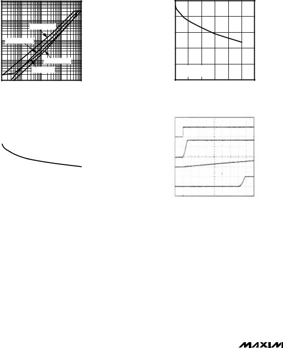
START-UP WAVEFORMS |
||||
|
|
|
|
vs. OUTPUT CURRENT |
|
|
|
|
|||||
|
2.510 |
|
|
|
|
|
|
|
|
|
MAX 1630/35-12 |
RUN |
MAX1630/35-13 |
|
|
|
|
|
|
|
|
|
|
||||
|
2.505 |
|
|
|
|
|
|
|
|
|
|||
|
|
|
|
|
|
|
|
|
|
||||
(V) |
|
|
|
|
|
|
|
|
|
|
|
5V/div |
|
|
|
|
|
|
|
|
|
|
|
|
2V/div |
|
|
VOLTAGE |
2.500 |
|
|
|
|
|
|
|
|
|
|
|
|
|
|
|
|
|
|
|
|
|
|
|
|
3.3V OUTPUT |
|
OUTPUT |
2.495 |
|
|
|
|
|
|
|
|
|
|
5V/div |
|
|
|
|
|
|
|
|
|
|
|
|
|||
|
|
|
|
|
|
|
|
|
|
|
|
||
|
|
|
|
|
|
|
|
|
|
|
|
TIME |
|
REF |
2.490 |
|
|
|
|
|
|
|
|
|
|
5V OUTPUT |
|
|
|
|
|
|
|
|
|
|
|
|
|||
|
|
|
|
|
|
|
|
|
|
|
|
||
|
2.485 |
|
|
|
|
|
|
|
|
|
|
|
|
|
|
VIN = 15V |
|
|
|
|
|
|
5V/div |
|
|||
|
|
|
|
|
|
|
|
|
|||||
|
|
|
ON3 = ON5 = 0V |
|
|
|
|
|
|
|
|
||
|
2.480 |
|
|
|
|
|
|
|
|
|
|
|
2ms/div |
|
|
|
|
|
|
|
|
|
|
|
|
||
|
0 |
1 |
2 |
3 |
4 |
5 |
6 |
|
|||||
|
|
|
|
OUTPUT CURRENT (mA) |
|
|
|
|
SEQ = VL, 0.015μF CAPACITOR ON-TIME |
||||
__________________________________________________________________________Pin Description
PIN |
NAME |
FUNCTION |
|
|
|
|
|
1 |
CSH3 |
Current-Sense Input for the 3.3V SMPS. Current-limit level is 100mV referred to CSL3. |
|
|
|
|
|
2 |
CSL3 |
Current-Sense Input. Also serves as the feedback input in fixed-output mode. |
|
|
|
|
|
|
|
Feedback Input for the 3.3V SMPS; regulates at FB3 = REF (approx. 2.5V) in adjustable mode. FB3 is a |
|
3 |
FB3 |
Dual Mode input that also selects the 3.3V fixed output voltage setting when tied to GND. Connect FB3 |
|
|
|
to a resistor divider for adjustable-output mode. |
|
|
|
|
|
|
12OUT |
12V/120mA Linear Regulator Output. Input supply comes from VDD. Bypass 12OUT to GND with |
|
|
(MAX1630/ |
||
|
1µF minimum. |
||
|
32/33/35) |
||
|
|
||
4 |
|
|
|
STEER |
Logic-Control Input for secondary feedback. Selects the PWM that uses a transformer and secondary |
||
|
|||
|
feedback signal (SECFB): |
||
|
(MAX1631/ |
||
|
STEER = GND: 3.3V SMPS uses transformer |
||
|
MAX1634) |
||
|
STEER = VL: 5V SMPS uses transformer |
||
|
|
||
|
|
|
6 _______________________________________________________________________________________

Multi-Output, Low-Noise Power-Supply
Controllers for Notebook Computers
_________________________________________________Pin Description (continued)
PIN |
NAME |
FUNCTION |
|
|
|
|
|
|
VDD |
Supply Voltage Input for the 12OUT Linear Regulator. Also connects to an internal resistor divider for |
|
|
(MAX1630/ |
||
|
secondary winding feedback, and to an 18V overvoltage shunt regulator clamp. |
||
|
32/33/35) |
||
5 |
|
||
|
|
||
SECFB |
Secondary Winding Feedback Input. Normally connected to a resistor divider from an auxiliary output. |
||
|
|||
|
(MAX1631/ |
SECFB regulates at VSECFB = 2.5V (see Secondary Feedback Regulation Loop section). Tie to VL if not |
|
|
MAX1634) |
used. |
|
|
|
|
|
6 |
SYNC |
Oscillator Synchronization and Frequency Select. Tie to VL for 300kHz operation; tie to GND for 200kHz |
|
operation. Can be driven at 240kHz to 350kHz for external synchronization. |
|||
|
|
||
|
|
|
|
7 |
TIME/ON5 |
Dual-Purpose Timing Capacitor Pin and ON/OFF Control Input. See Power-Up Sequencing and |
|
ON/OFF Controls section. |
|||
|
|
||
|
|
|
|
8 |
GND |
Low-Noise Analog Ground and Feedback Reference Point |
|
|
|
|
|
9 |
REF |
2.5V Reference Voltage Output. Bypass to GND with 1µF minimum. |
|
|
|
|
|
10 |
SKIP |
Logic-Control Input that disables Idle Mode when high. Connect to GND for normal use. |
|
|
|
|
|
11 |
RESET |
Active-Low Timed Reset Output. RESET swings GND to VL. Goes high after a fixed 32,000 clock-cycle |
|
delay following power-up. |
|||
|
|
||
|
|
|
|
|
|
Feedback Input for the 5V SMPS; regulates at FB5 = REF (approx. 2.5V) in adjustable mode. FB5 is a |
|
12 |
FB5 |
Dual Mode input that also selects the 5V fixed output voltage setting when tied to GND. Connect FB5 to |
|
|
|
a resistor divider for adjustable-output mode. |
|
|
|
|
|
13 |
CSL5 |
Current-Sense Input for the 5V SMPS. Also serves as the feedback input in fixed-output mode, and as |
|
the bootstrap supply input when the voltage on CSL5/VL is > 4.5V. |
|||
|
|
||
|
|
|
|
14 |
CSH5 |
Current-Sense Input for the 5V SMPS. Current-limit level is 100mV referred to CSL5. |
|
|
|
|
|
|
|
Pin-Strap Input that selects the SMPS power-up sequence: |
|
15 |
SEQ |
SEQ = GND: 5V before 3.3V, RESET output determined by both outputs |
|
SEQ = REF: Separate ON3/ON5 controls, RESET output determined by 3.3V output |
|||
|
|
||
|
|
SEQ = VL: 3.3V before 5V, RESET output determined by both outputs |
|
|
|
|
|
16 |
DH5 |
Gate-Drive Output for the 5V, high-side N-channel switch. DH5 is a floating driver output that swings |
|
from LX5 to BST5, riding on the LX5 switching node voltage. |
|||
|
|
||
|
|
|
|
17 |
LX5 |
Switching Node (inductor) Connection. Can swing 2V below ground without hazard. |
|
|
|
|
|
18 |
BST5 |
Boost capacitor connection for high-side gate drive (0.1µF) |
|
|
|
|
|
19 |
DL5 |
Gate-Drive Output for the low-side synchronous-rectifier MOSFET. Swings 0V to VL. |
|
|
|
|
|
20 |
PGND |
Power Ground |
|
|
|
|
|
|
|
5V Internal Linear-Regulator Output. VL is also the supply voltage rail for the chip. After the 5V SMPS |
|
21 |
VL |
output has reached +4.5V (typical), VL automatically switches to the output voltage via CSL5 for boot- |
|
|
|
strapping. Bypass to GND with 4.7µF. VL supplies up to 25mA for external loads. |
|
|
|
|
|
22 |
V+ |
Battery Voltage Input, +4.2V to +30V. Bypass V+ to PGND close to the IC with a 0.22µF capacitor. |
|
Connects to a linear regulator that powers VL. |
|||
|
|
||
|
|
|
|
23 |
SHDN |
Shutdown Control Input, active low. Logic threshold is set at approximately 1V. For automatic start-up, |
|
connect SHDN to V+ through a 220kΩ resistor and bypass SHDN to GND with a 0.01µF capacitor. |
|||
|
|
||
|
|
|
|
24 |
DL3 |
Gate-Drive Output for the low-side synchronous-rectifier MOSFET. Swings 0V to VL. |
|
|
|
|
|
25 |
BST3 |
Boost Capacitor Connection for high-side gate drive (0.1µF) |
|
|
|
|
|
26 |
LX3 |
Switching Node (inductor) Connection. Can swing 2V below ground without hazard. |
|
|
|
|
|
27 |
DH3 |
Gate-Drive Output for the 3.3V, high-side N-channel switch. DH3 is a floating driver output that swings |
|
from LX3 to BST3, riding on the LX3 switching node voltage. |
|||
|
|
||
|
|
|
|
28 |
RUN/ON3 |
ON/OFF Control Input. See Power-Up Sequencing and ON/OFF Controls section. |
|
|
|
|
MAX1635–MAX1630
_______________________________________________________________________________________ 7

Multi-Output, Low-Noise Power-Supply Controllers for Notebook Computers
MAX1630–MAX1635 |
|
|
INPUT |
|
ON/OFF |
|
|
|
|
|
|
|
|
|
|
+5V ALWAYS ON |
|
|
|||
|
|
|
|
|
|
|
|
|||
|
|
C3 |
|
|
|
4.7μF |
|
|
|
|
|
|
|
|
10Ω |
|
|
|
|
||
|
|
|
|
|
0.1μF |
|
|
|
||
|
|
|
|
0.1μF |
|
|
|
|
||
|
|
|
|
V+ SHDN SECFB VL |
|
|
|
|
||
|
|
|
|
4.7μF |
SYNC |
|
|
|
|
|
|
|
|
|
BST5 |
BST3 |
|
|
|
|
|
|
|
|
|
|
|
|
|
|
||
|
|
|
Q1 |
DH5 |
DH3 |
Q3 |
|
|
|
|
|
|
|
0.1μF |
0.1μF |
0.1μF |
0.1μF |
|
|
|
|
+5V OUTPUT |
|
R1 |
L1 |
LX5 |
LX3 |
L2 |
R2 |
+3.3V OUTPUT |
||
C1 |
* |
|
Q2 |
DL5 |
MAX1631 |
|
|
* |
C2 |
|
|
|
|
|
|
MAX1634 DL3 |
Q4 |
|
|
|
|
|
|
|
|
PGND |
|
|
|
|
||
|
|
|
|
CSH5 |
CSH3 |
|
|
|
|
|
|
|
|
|
|
CSL5 |
CSL3 |
|
|
|
|
|
|
|
|
|
|
FB3 |
|
|
|
|
|
|
|
|
|
FB5 |
|
|
|
|
|
|
|
|
|
|
|
RESET |
RESET OUTPUT |
|
|
|
|
|
|
|
|
|
|
|
|
|
|
|
|
|
5V ON/OFF |
|
TIME/ON5 |
|
|
|
|
|
|
|
|
3.3V ON/OFF |
|
|
SKIP |
|
|
|
|
|
|
|
|
RUN/ON3 |
|
|
|
|
||
|
|
|
|
|
|
STEER |
|
|
|
|
|
|
|
|
|
GND |
|
|
|
|
|
|
|
|
|
|
REF |
SEQ |
|
|
|
|
|
|
|
|
|
|
|
+2.5V ALWAYS ON |
|
|
|
|
|
|
|
|
|
1μF |
|
|
|
|
|
|
|
|
|
|
*1A SCHOTTKY DIODE REQUIRED |
|
|
|
|
|
|
|
|
|
|
FOR THE MAX1631 (SEE OUTPUT |
|
|
|
|
|
|
|
|
|
|
OVERVOLTAGE PROTECTION SECTION). |
|
|
|
|
Figure 1. Standard 3.3V/5V Application Circuit (MAX1631/MAX1634)
_______Standard Application Circuit
The basic MAX1631/MAX1634 dual-output 3.3V/5V buck converter (Figure 1) is easily adapted to meet a wide range of applications with inputs up to 28V by substituting components from Table 1. These circuits represent a good set of tradeoffs between cost, size, and efficiency, while staying within the worst-case specification limits for stress-related parameters, such as capacitor ripple current. Don’t change the frequency
of these circuits without first recalculating component values (particularly inductance value at maximum battery voltage). Adding a Schottky rectifier across each synchronous rectifier improves the efficiency of these circuits by approximately 1%, but this rectifier is otherwise not needed because the MOSFETs required for these circuits typically incorporate a high-speed silicon diode from drain to source. Use a Schottky rectifier rated at a DC current equal to at least one-third of the load current.
8 _______________________________________________________________________________________

Multi-Output, Low-Noise Power-Supply
Controllers for Notebook Computers
Table 1. Component Selection for Standard 3.3V/5V Application
COMPONENT |
|
|
LOAD CURRENT |
|
|
|
|
|
|
||
2A |
3A |
4A |
|||
|
|
||||
|
|
|
|
|
|
Input Range |
4.75V to 18V |
4.75V to 28V |
4.75V to 24V |
||
|
|
|
|
|
|
Application |
|
PDA |
Notebook |
Workstation |
|
|
|
|
|
|
|
Frequency |
|
300kHz |
300kHz |
200kHz |
|
|
|
|
|
|
|
|
|
1/2 IR IRF7301; |
IR IRF7403 or IRF7401 (18V |
IR IRF7413 or |
|
Q1, Q3 High-Side |
|
1/2 Siliconix Si9925DQ; or |
max); Siliconix Si4412DY; or |
Siliconix Si4410DY |
|
MOSFETs |
|
1/2 Motorola MMDF3N03HD or |
Motorola MMSF5N03HD or |
|
|
|
|
MMDF4N01HD (10V max) |
MMSF5N02HD (18V max) |
|
|
|
|
|
|
|
|
|
|
1/2 IR IRF7301; |
IR IRF7403 or IRF7401 (18V |
IR IRF7413 or |
|
Q2, Q4 Low-Side |
|
1/2 Siliconix Si9925DQ; or |
max); Siliconix Si4412DY; or |
Siliconix Si4410DY |
|
MOSFETs |
|
1/2 Motorola MMDF3N03HD or |
Motorola MMSF5N03HD or |
|
|
|
|
MMDF4N01HD (10V max) |
MMSF5N02HD (18V max) |
|
|
|
|
|
|
|
|
|
|
10µF, 30V Sanyo OS-CON; |
2 x 10µF, 30V Sanyo OS-CON; |
3 x 10µF, 30V Sanyo OS-CON; |
|
C3 Input Capacitor |
|
22µF, 35V AVX TPS; or |
2 x 22µF, 35V AVX TPS; or |
4 x 22µF, 35V AVX TPS; or |
|
|
|
Sprague 594D |
Sprague 594D |
Sprague 595D |
|
|
|
|
|
|
|
C1, C2 Output Capacitors |
|
220µF, 10V AVX TPS or |
2 x 220µF, 10V AVX TPS or |
4 x 220µF, 10V AVX TPS or |
|
|
Sprague 595D |
Sprague 595D |
Sprague 595D |
||
|
|
||||
|
|
|
|
|
|
R1, R2 Resistors |
|
0.033Ω IRC LR2010-01-R033 or |
0.02Ω IRC LR2010-01-R020 or |
0.012Ω Dale WSL2512-R012-F |
|
|
Dale WSL2010-R033-F |
Dale WSL2010-R020-F |
|
||
|
|
|
|||
|
|
|
|
|
|
|
|
15µH, 2.4A Ferrite |
10µH, 4A Ferrite |
4.7µH, 5.5A Ferrite |
|
L1, L2 Inductors |
Coilcraft DO3316P-153 or |
Coilcraft DO3316P-103 or |
Coilcraft DO3316-472 or |
||
Sumida CDRH125-150 |
Sumida CDRH125-100 |
5.2µH, 6.5A Ferrite Sumida |
|||
|
|
||||
|
|
|
|
CDRH127-5R2MC |
|
|
|
|
|
|
|
Table 2. Component Suppliers
COMPANY |
FACTORY FAX |
USA PHONE |
|
(COUNTRY CODE) |
|||
|
|
||
|
|
|
|
AVX |
(1) 803-626-3123 |
(803) 946-0690 |
|
|
|
|
|
Central |
(1) 516-435-1824 |
(516) 435-1110 |
|
Semiconductor |
|||
|
|
||
|
|
|
|
Coilcraft |
(1) 847-639-1469 |
(847) 639-6400 |
|
|
|
|
|
Coiltronics |
(1) 561-241-9339 |
(561) 241-7876 |
|
|
|
|
|
Dale |
(1) 605-665-1627 |
(605) 668-4131 |
|
|
|
|
|
International |
(1) 310-322-3332 |
(310) 322-3331 |
|
Rectifier (IR) |
|||
|
|
||
|
|
|
|
IRC |
(1) 512-992-3377 |
(512) 992-7900 |
|
|
|
|
|
Matsuo |
(1) 714-960-6492 |
(714) 969-2491 |
|
|
|
|
*Distributor
COMPANY |
|
|
FACTORY FAX |
USA PHONE |
|
|
|
(COUNTRY CODE) |
|||
|
|
|
|
|
|
|
|
|
|
|
|
Motorola |
|
(1) 602-994-6430 |
(602) |
303-5454 |
|
|
|
|
|
|
|
Murata-Erie |
|
|
(1) 814-238-0490 |
(814) |
237-1431 |
|
|
|
|
|
|
NIEC |
|
(81) 3-3494-7414 |
(805) |
867-2555* |
|
|
|
|
|
|
|
Sanyo |
|
|
(81) 7-2070-1174 |
(619) |
661-6835 |
|
|
|
|
|
|
Siliconix |
|
(1) 408-970-3950 |
(408) |
988-8000 |
|
|
|
|
|
|
|
Sprague |
|
|
(1) 603-224-1430 |
(603) |
224-1961 |
|
|
|
|
|
|
Sumida |
|
|
(81) 3-3607-5144 |
(847) |
956-0666 |
|
|
|
|
|
|
TDK |
|
|
(1) 847-390-4428 |
(847) |
390-4373 |
|
|
|
|
|
|
Transpower |
|
|
(1) 702-831-3521 |
(702) |
831-0140 |
Technologies |
|
|
|||
|
|
|
|
|
|
|
|
|
|
|
|
MAX1635–MAX1630
_______________________________________________________________________________________ 9
 Loading...