


KIT
EVALUATION
AVAILABLE
SPDT Negative Rail Analog Switches
with ±VCC Capability
General Description
The MAX14504/MAX14505/MAX14505A/MAX14506 dual single-pole/double-throw (SPDT) audio switches feature negative signal capability that allows signals from -VCC to +VCC to pass without distortion. They feature high continuous current ratings of 550mA (continuous) and 850mA (pulsed). These analog switches have low on-resistance, low supply current, and operate from a single +2.3V to +5.5V supply.
The MAX14505/MAX14505A have internal shunt switches that discharge the audio amplifier AC-coupling capacitance at the normally open (NO) terminals. This reduces click-and-pop sounds that occur when switching audio signals between precharged points. The MAX14504/ MAX14505/MAX14505A/MAX14506 control the switches with control bit, CB, and feature an enable input, EN, that place COM in a high-impedance mode.
Features
♦Distortion-Free Negative Signal Throughput from -VCC to +VCC
♦Internal Shunt Switches Reduce Click/Pop (MAX14505/MAX14505A)
♦Low On-Resistance 0.36Ω (typ)
♦1mΩ (typ) On-Resistance Flatness
♦COM High Impedance for EN = High
♦Low 0.2µA (max) Shutdown Current (MAX14505A/MAX14506)
♦+2.3V to +5.5V Single-Supply Voltage
♦Small, 1.56mm x 2.14mm, 12-Bump WLP Package
The MAX14504/MAX14505/MAX14505A/MAX14506 are fully specified to operate from a single +2.3V to +5.5V power supply. These devices are available in a 1.56mm x 2.14mm, 12-bump WLP package, and operate over the -40°C to +85°C extended temperature range.
Applications
Cell Phones
MP3 Players
Portable Audio Equipment
Speaker Switching
Typical Operating Circuit appears at end of data sheet.
|
Pin Configuration |
||
|
MAX14504/ |
|
|
TOP VIEW |
MAX14505/ |
|
|
MAX14505A/ |
|
||
(BUMPS ON BOTTOM) |
MAX14506 |
|
|
|
|
||
1 |
2 |
3 |
4 |
+ |
|
|
|
NO2 |
NEG |
VCC |
NO1 |
A |
|
|
|
COM2 |
EN |
GND |
COM1 |
B |
|
|
|
NC2 |
CB |
GND |
NC1 |
C |
|
|
|
|
WLP |
|
|
(1.56mm x 2.14mm) |
|
||
|
|
|
Ordering Information/Selector Guide |
|||
|
|
|
|
|
|
|
PART |
PIN-PACKAGE |
TOP MARK |
COM SIGNAL RANGE FOR |
CLICKLESS |
||
EN = VCC |
||||||
|
|
|
|
|
||
MAX14504EWC+ |
12 WLP |
AAH |
±VCC |
NO |
||
MAX14505EWC+* |
12 WLP |
AAI |
±VCC |
YES |
||
MAX14505AEWC+ |
12 WLP |
AAK |
0 to +VCC |
YES |
||
MAX14506EWC+* |
12 WLP |
AAJ |
0 to +VCC |
NO |
||
|
|
|
|
|
|
|
Note: All devices are specified over the -40°C to +85°C temperature range. +Denotes a lead(Pb)-free/RoHS-compliant package.
*Future product—contact factory for availability.
________________________________________________________________ Maxim Integrated Products 1
For pricing, delivery, and ordering information, please contact Maxim Direct at 1-888-629-4642, or visit Maxim’s website at www.maxim-ic.com.
MAX14504/MAX14505/MAX14505A/MAX14506

MAX14504/MAX14505/MAX14505A/MAX14506
Dual SPDT Negative Rail Analog Switches with ±VCC Capability
ABSOLUTE MAXIMUM RATINGS
(All voltages referenced to GND, unless otherwise noted.) |
Continuous Power Dissipation (TA = +70°C) for multilayer board: |
|||
VCC ........................................................................ |
|
- 0.3V to +6.0V |
12-Pin WLP (derate 8.5mW/°C above +70°C) |
..............678mW |
NC_, NO_, COM_ (Note 1).................. |
-VCC - 0.3V to VCC + 0.3V |
Operating Temperature Range ........................... |
-40°C to +85°C |
|
NC_, NO_, COM_ (MAX14505A/MAX14506, EN = VCC) |
Junction Temperature ...................................................... |
+150°C |
||
(Note 1) ....................................................... |
|
- 0.3V to V CC + 0.3V |
Storage Temperature Range ............................. |
-65°C to +150°C |
CB, EN...................................................................... |
|
- 0.3V to +6V |
Package Junction-to-Ambient Thermal |
|
Continuous Current (NC_, NO_, COM_) |
.........................±550mA |
Resistance (θJA) (Note 2)............................................ |
118°C/W |
|
Continuous Current on Shunt Switches .............................. |
±5mA |
Lead Temperature (soldering) ......................................... |
+300°C |
|
Peak Current (NC_, NO_, COM_) |
|
|
|
|
(pulsed at 1ms, 10% duty cycle).................................. |
|
±850mA |
|
|
Note 1: Signals on NC_, NO_, and COM_ exceeding -VCC or +VCC are clamped by internal diodes. For EN ≥ VIH signals on NC_, NO_, and COM_ exceeding 0 or +VCC are clamped by internal diodes (MAX14505A/MAX14506). Limit forward-diode current to maximum current rating.
Note 2: Package thermal resistances were obtained using the method described in JEDEC specification JESD51-7, using a 4-layer board. For detailed information on package thermal considerations, refer to www.maxim-ic.com/thermal-tutorial.
Stresses beyond those listed under “Absolute Maximum Ratings” may cause permanent damage to the device. These are stress ratings only, and functional operation of the device at these or any other conditions beyond those indicated in the operational sections of the specifications is not implied. Exposure to absolute maximum rating conditions for extended periods may affect device reliability.
ELECTRICAL CHARACTERISTICS
(VCC = +2.3 to +5.5V, TA = TMIN to TMAX, CNEG = 3.3nF, unless otherwise noted. Typical values are at VCC = +3.0V, TA = +25°C, unless otherwise noted.) (Note 3)
PARAMETER |
SYMBOL |
CONDITIONS |
MIN |
TYP |
MAX |
UNITS |
|
|
|
|
|
|
|
|
|
ANALOG SWITCH |
|
|
|
|
|
|
|
|
|
|
|
|
|
|
|
|
|
VEN = 0 |
|
-VCC |
|
+VCC |
|
|
NC_, NO_, |
|
(MAX14504/ |
-VCC |
|
+VCC |
|
Analog Signal Range |
|
MAX14505) |
|
V |
|||
COM_ |
VEN = VCC |
|
|
|
|||
|
|
|
|
|
|
||
|
(MAX14505A/ |
0 |
|
+VCC |
|
||
|
|
|
|
|
|||
|
|
|
MAX14506) |
|
|
||
|
|
|
|
|
|
|
|
|
|
|
|
|
|
|
|
|
|
VCC = +3.0V, |
TA = +25°C |
|
0.36 |
0.5 |
|
On-Resistance |
RON |
ICOM_ = 50mA, |
|
|
|
|
Ω |
VNC_, VNO_ = |
TA = TMIN to |
|
|
0.65 |
|||
|
|
|
|
|
|||
|
|
-VCC to VCC |
TMAX |
|
|
|
|
|
|
|
|
|
|
||
On-Resistance Match |
∆RON |
VCC = +3.0V, INC_ = INO_ = 50mA; |
|
10 |
|
mΩ |
|
Between Channels |
between NC_ and NO_ only |
|
|
||||
|
|
|
|
|
|||
|
|
|
|
|
|
|
|
On-Resistance Flatness |
RFLAT (ON) |
VCC = +3.0V, INC_ = INO_ = 50mA, |
|
1 |
|
mΩ |
|
VNC_, VNO_ = -VCC to VCC (Note 4) |
|
|
|||||
|
|
|
|
|
|
||
Shunt Switch Resistance |
RSHUNT |
VNO_ = +100mV |
|
15 |
55 |
120 |
Ω |
2 _______________________________________________________________________________________ 


Dual SPDT Negative Rail Analog Switches
with ±VCC Capability
ELECTRICAL CHARACTERISTICS (continued)
(VCC = +2.3 to +5.5V, TA = TMIN to TMAX, CNEG = 3.3nF, unless otherwise noted. Typical values are at VCC = +3.0V, TA = +25°C, unless otherwise noted.) (Note 3)
PARAMETER |
SYMBOL |
CONDITIONS |
MIN |
TYP |
MAX |
UNITS |
|
|
|
|
|
|
|
|
|
VCC = +3.0V, switch open; |
|
|
|
|
|
|
VNO_ = -2.5V, +2.5V; |
-50 |
|
+50 |
|
|
|
VCOM_ = +2.5V, -2.5V, unconnected |
|
|
||
NC_ or NO_ Off-Leakage |
INC_ (OFF), |
|
|
|
|
|
(MAX14504/MAX14506) |
|
|
|
nA |
||
Current |
INO_ (OFF) |
|
|
|
|
|
VCC = +3.0V, switch open; |
|
|
|
|
||
|
|
|
|
|
|
|
|
|
VNC_ = -2.5V, +2.5V; |
-50 |
|
+50 |
|
|
|
VCOM_ = +2.5V, -2.5V, unconnected |
|
|
|
|
COM_ On-Leakage |
|
VCC = +3.0V, switch closed; |
|
|
|
|
ICOM_ (ON) |
VCOM_ = +2.5V, -2.5V ; |
-100 |
|
+100 |
nA |
|
Current |
|
|||||
|
VNC_ or VNO_ = +2.5V, -2.5V, unconnected |
|
|
|
|
|
|
|
|
|
|
|
|
DYNAMIC TIMING (Note 5) |
|
|
|
|
|
|
|
|
|
|
|
|
|
Turn-On Time |
tON |
VNO_ or VNC_ = 0, RL = 50Ω, Figure 1 |
|
14 |
60 |
ms |
Turn-Off Time |
tOFF |
VNO_ or VNC_ = 0, RL = 50Ω, Figure 1 |
|
1.5 |
3 |
µs |
AUDIO PERFORMANCE |
|
|
|
|
|
|
|
|
|
|
|
|
|
Total Harmonic Distortion Plus |
THD+N |
f = 20Hz to 20kHz, VCOM_ = 0.5VP-P, |
|
0.001 |
|
% |
Noise |
RS = RL = 50Ω; DC bias = 0 |
|
|
|||
|
|
|
|
|
||
Off-Isolation |
VISO |
RS = RL = 50Ω; VCOM_ = 0.5VP-P, |
|
-84 |
|
dB |
f = 20kHz (Note 6), Figure 2 |
|
|
||||
|
|
|
|
|
|
|
|
|
|
|
|
|
|
Crosstalk |
VCT |
RS = RL = 50Ω; VCOM_ = 0.5VP-P, |
|
-90 |
|
dB |
f = 20kHz (Note 7), Figure 2 |
|
|
||||
|
|
|
|
|
|
|
|
|
|
|
|
|
|
NC_ or NO_ Off-Capacitance |
CNC_ (OFF), |
VNC_/NO_ = 0.5VP-P, f = 1MHz; Figure 3 |
|
65 |
|
pF |
CNO_ (OFF) |
|
|
||||
|
|
|
|
|
|
|
|
|
|
|
|
|
|
COM_ On-Capacitance |
CCOM_ (ON) |
VNC_/NO_ = 0.5VP-P, f = 1MHz; Figure 3 |
|
125 |
|
pF |
LOGIC INPUT (CB, EN) |
|
|
|
|
|
|
|
|
|
|
|
|
|
Input Logic-High |
VIH |
|
1.4 |
|
|
V |
Input Logic-Low |
VIL |
|
|
|
0.5 |
V |
Input Leakage Current |
IIN |
VCB = VEN = 0 or VCC |
-1 |
|
+1 |
µA |
|
|
|
|
|
|
|
MAX14504/MAX14505/MAX14505A/MAX14506
_______________________________________________________________________________________ 3
MAX14504/MAX14505/MAX14505A/MAX14506
Dual SPDT Negative Rail Analog Switches with ±VCC Capability
ELECTRICAL CHARACTERISTICS (continued)
(VCC = +2.3 to +5.5V, TA = TMIN to TMAX, CNEG = 3.3nF, unless otherwise noted. Typical values are at VCC = +3.0V, TA = +25°C, unless otherwise noted.) (Note 3)
PARAMETER |
SYMBOL |
CONDITIONS |
MIN |
TYP |
MAX |
UNITS |
|
|
|
|
|
|
|
POWER SUPPLY |
|
|
|
|
|
|
|
|
|
|
|
|
|
Power-Supply Range |
VCC |
|
2.3 |
|
5.5 |
V |
Power-Supply Rejection Ratio |
|
RCOM_ = 50Ω, f = 10kHz |
|
78 |
|
dB |
(PSRR) |
|
|
|
|||
|
|
|
|
|
|
|
|
|
|
|
|
|
|
VCC Supply Current |
ICC |
VCC = +3.0V, VEN = 0, VCB = 0 or VCC |
|
12 |
23 |
µA |
VCC = +5.5V, VEN = 0, VCB = 0 or VCC |
|
21 |
41 |
|||
|
|
|
|
|||
|
|
VCC = +3.0V, VEN = VCC |
|
|
15 |
|
|
|
(MAX14504/MAX14505) |
|
|
|
|
|
|
|
|
|
|
|
|
|
|
|
|
|
|
|
|
VCC = +5.5V, VEN = VCC |
|
|
29 |
|
|
|
(MAX14504/MAX14505) |
|
|
|
|
VCC Shutdown Supply Current |
ICC_SHDN |
|
|
|
µA |
|
|
|
|
|
|||
VCC = +3.0V, VEN = VCC |
|
|
0.15 |
|||
|
|
|
|
|
||
|
|
(MAX14505A/MAX14506) |
|
|
|
|
|
|
|
|
|
|
|
|
|
|
|
|
|
|
|
|
VCC = +5.5V, VEN = VCC |
|
|
0.2 |
|
|
|
(MAX14505A/MAX14506) |
|
|
|
|
|
|
|
|
|
|
|
|
|
|
|
|
|
|
Supply Current Increase with |
ICC_CTRL |
VCC = 5.5V, VCB = VEN = 0.5V or 1.4V |
|
2 |
5 |
µA |
Supply Voltage |
|
|||||
|
|
|
|
|
|
|
|
|
|
|
|
|
|
Negative Charge-Pump Output |
VNEG |
CNEG = 3.3nF |
-1.01VCC |
-VCC |
-0.95VCC |
V |
|
|
|
|
|
|
|
Note 3: All parameters are production tested at TA = +85°C, and guaranteed by design over the specified temperature range. Note 4: Flatness is defined as the difference between the maximum and minimum value of on-resistance as measured over the
specified analog signal range.
Note 5: All timing is measured using 20% and 80% levels.
Note 6: Off-Isolation = 20log10[VCOM_/(VNO_ or VNC_)], VCOM_ = output, VNO_ or VNC_ = input to off switch. Note 7: Between any two switches.
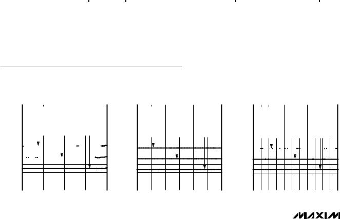
Typical Operating Characteristics
(VCC = 3.0V, TA = +25°C, unless otherwise noted.)
|
1.0 |
|
|
ON-RESISTANCE vs. VCOM |
|
|
1.0 |
|
|
ON-RESISTANCE vs. VCOM |
|
|
|
|
|
|
|
|
|
ON-RESISTANCE vs. VCOM |
|||||||||||||||||||||||||||||||||||||||||
|
|
|
|
|
|
|
|
|
|
|
|
|
|
|
|
|
|
toc01 |
|
|
|
|
|
|
|
|
|
|
|
|
|
|
|
|
|
|
|
toc02 |
|
1.0 |
|
|
|
|
|
|
|
|
|
|
|
|
|
|
|
|
|
|
toc03 |
||
|
0.9 |
|
VCC = 2.3V |
|
|
|
|
|
|
|
|
|
|
|
|
0.9 |
|
VCC = 3.0V |
|
|
|
|
|
|
|
|
|
|
|
|
|
|
0.9 |
|
VCC = 5.5V |
|
|
|
|
|
|
|
|
|
|
|
|
||||||||||||||
|
|
|
|
|
|
|
|
|
|
|
|
|
|
|
|
|
|
MAX14504 |
|
|
|
|
|
|
|
|
|
|
|
|
|
|
|
|
|
|
|
MAX14504 |
|
|
|
|
|
|
|
|
|
|
|
|
|
|
|
|
|
|
|
MAX14504 |
|||
|
|
|
|
|
|
|
|
|
|
|
|
|
|
|
|
|
|
|
|
|
|
|
|
|
|
|
|
|
|
|
|
|
|
|
|
|
|
|
|
|
|
|
|
|
|
|
|
|
|
|
|
|
|
|
|
||||||
|
0.8 |
|
|
|
|
|
|
|
|
|
|
|
|
|
|
|
|
|
|
0.8 |
|
|
|
|
|
|
|
|
|
|
|
|
|
|
|
|
|
|
|
0.8 |
|
|
|
|
|
|
|
|
|
|
|
|
|
|
|
|
|
|
|||
|
|
|
|
|
|
|
|
|
|
|
|
|
|
|
|
|
|
|
|
|
|
|
|
|
|
|
|
|
|
|
|
|
|
|
|
|
|
|
|
|
|
|
|
|
|
|
|
|
|
|
|
|
|
|
|
||||||
|
0.7 |
|
|
|
|
|
|
|
|
|
|
|
|
|
|
|
|
|
|
|
0.7 |
|
|
|
|
|
|
|
|
|
|
|
|
|
|
|
|
|
|
|
|
0.7 |
|
|
|
|
|
|
|
|
|
|
|
|
|
|
|
|
|
|
|
|
|
|
TA = +85°C |
|
TA = +25°C |
|
|
|
TA = -40°C |
|
|
|
|
|
|
|
|
|
° |
|
|
|
|
° |
|
|
|
° |
|
|
|
|
|
|
|
|
|
|
|
|
|
|
|
|
|
|
|
|
|
|
|
||||||||||
(Ω) |
0.6 |
|
|
|
|
|
|
|
|
|
|
|
|
|
|
|
|
|
|
(Ω) |
0.6 |
|
|
TA = |
+85 |
|
|
C |
|
TA = |
+25 C |
|
TA = -40 |
|
C |
|
|
(Ω) |
0.6 |
|
|
TA = +85°C |
|
TA = +25°C |
|
TA = -40°C |
|
||||||||||||||
|
|
|
|
|
|
|
|
|
|
|
|
|
|
|
|
|
|
|
|
|
|
|
|
|
|
|
|
|
|
|
|
|
|
|
|
|
|
|
|
|
|
|
|
|
|
|
|
|
|
|
|
|
|
|
|
||||||
|
|
|
|
|
|
|
|
|
|
|
|
|
|
|
|
|
|
|
|
|
|
|
|
|
|
|
|
|
|
|
|
|
|
|
|
|
|
|
|
|
|
|
|
|
|
|
|
|
|
|
|
|
|
|
|
||||||
0.5 |
|
|
|
|
|
|
|
|
|
|
|
|
|
|
|
|
|
|
0.5 |
|
|
|
|
|
|
|
|
|
|
|
|
|
|
|
|
|
|
|
0.5 |
|
|
|
|
|
|
|
|
|
|
|
|
|
|
|
|
|
|
|
|||
ON |
|
|
|
|
|
|
|
|
|
|
|
|
|
|
|
|
|
|
ON |
|
|
|
|
|
|
|
|
|
|
|
|
|
|
|
|
|
|
|
ON |
|
|
|
|
|
|
|
|
|
|
|
|
|
|
|
|
|
|
|
|||
|
|
|
|
|
|
|
|
|
|
|
|
|
|
|
|
|
|
|
|
|
|
|
|
|
|
|
|
|
|
|
|
|
|
|
|
|
|
|
|
|
|
|
|
|
|
|
|
|
|
|
|
|
|
|
|
|
|
|
|||
R |
0.4 |
|
|
|
|
|
|
|
|
|
|
|
|
|
|
|
|
|
|
R |
0.4 |
|
|
|
|
|
|
|
|
|
|
|
|
|
|
|
|
|
|
|
R |
0.4 |
|
|
|
|
|
|
|
|
|
|
|
|
|
|
|
|
|
|
|
|
|
|
|
|
|
|
|
|
|
|
|
|
|
|
|
|
|
|
|
|
|
|
|
|
|
|
|
|
|
|
|
|
|
|
|
|
|
|
|
|
|
|
|
|
|
|
|
|
|
|
|
|
|
|
|
|
|
|
|||
0.3 |
0.3 |
0.3 |
0.2 |
0.2 |
0.2 |
0.1 |
|
|
|
|
|
|
0.1 |
|
|
|
|
|
|
|
0.1 |
|
|
|
|
|
|
|
|
|
|
|
|
|
|
|
|
|
|||
0 |
|
|
|
|
|
|
0 |
|
|
|
|
|
|
|
0 |
|
|
|
|
|
|
|
|
|
|
|
|
|
|
|
|
|
|||
-2.30 |
-1.15 |
0 |
1.15 |
2.30 |
-3 |
-2 |
-1 |
0 |
1 |
2 |
3 |
-5.5 -4.5 -3.5 -2.5 -1.5 -0.5 0.5 1.5 2.5 3.5 4.5 5.5 |
|||||
|
|
|
VCOM (V) |
|
|
|
|
|
|
|
VCOM (V) |
|
|
|
|
VCOM (V) |
|
4 _______________________________________________________________________________________
 Loading...