

Page 1
Service
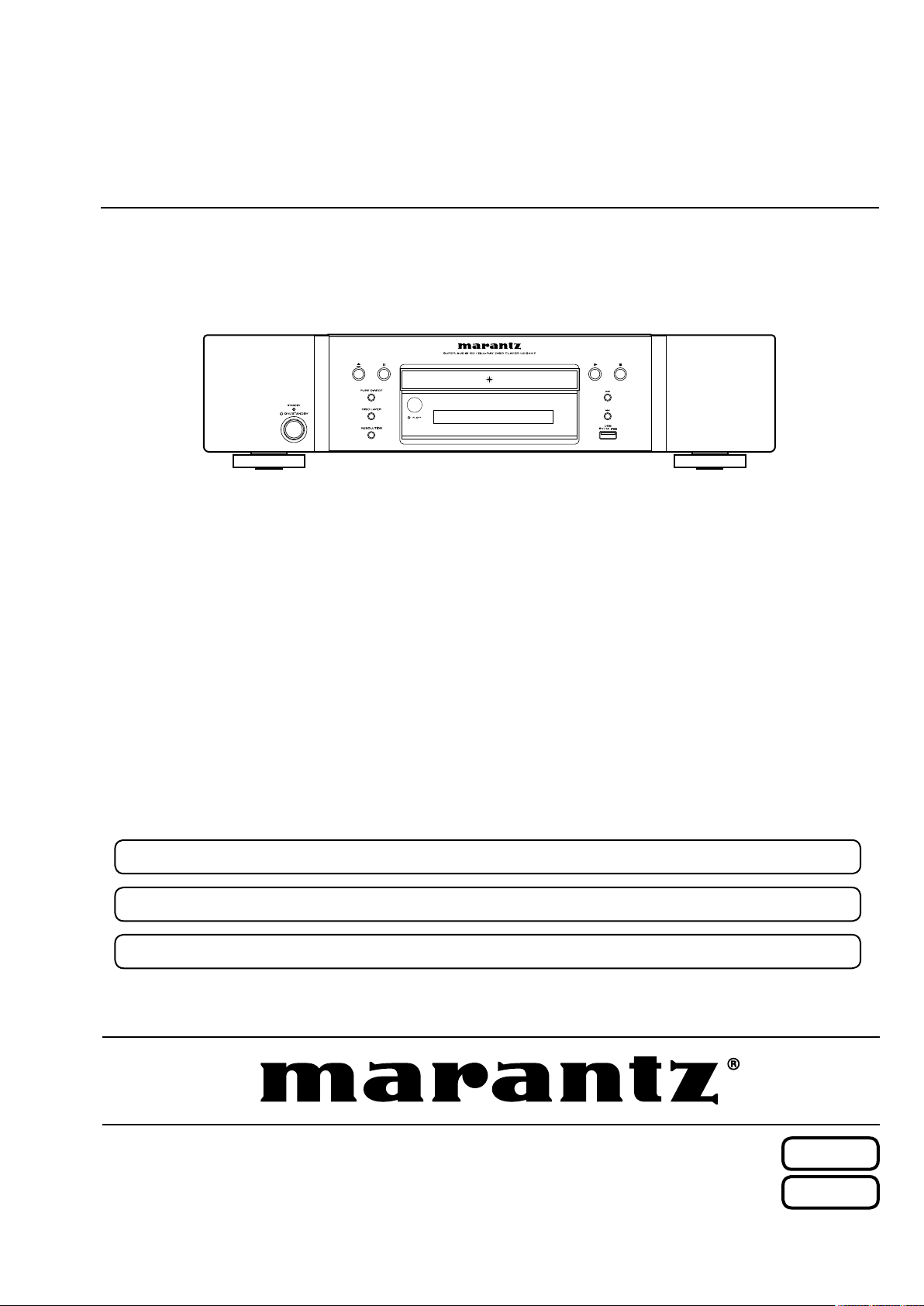
UD5007 /
U1B/K1B/S1B
N1SG/N1B
Manual
SUPER AUDIO CD/
BLU-RAY DISC PLAYER
For purposes of improvement, specications and design are subject to change without notice.
•
Please use this service manual with referring to the operating instructions without fail.
•
Some illustrations using in this service manual are slightly different from the actual set.
•
UD5007
S0690-0V07DM/DG1306
Ver. 7
Please refer to the
MODIFICATION NOTICE.
Page 2

CONTENTS
SAFETY PRECAUTIONS
NOTE FOR SCHEMATIC DIAGRAM
NOTE FOR PARTS LIST
WARNING AND LASER SAFETY INSTRUCTIONS
INSTRUCTIONS FOR HANDLING SEMI-CONDUCTORS
AND OPTICAL UNIT
1. Ground for Human Body .......................................................7
2. Ground for Workbench ..........................................................7
TECHNICAL SPECIFICATIONS
DIMENSION
CAUTIONS IN SERVICING
Initializing BD player ..................................................................9
Service tools ..............................................................................9
DISASSEMBLY
1. FRONT PANEL ASSY .........................................................11
2. BD MECHA UNIT ASSY .....................................................12
3. MAIN PCB UNIT ASSY .......................................................13
4. POWER PCB UNIT ASSY ..................................................14
5. IR PCB UNIT ASSY ............................................................14
REMOVING DISCS .................................................................15
DIAGNOSTICS OF OPTICAL PICKUP
1. Iop checked Method ............................................................17
2. To clear the accumulated laser on time ...............................17
HOW TO REPLACE THE MAIN PCB & BD MECHA
OR BD MECHA
1. How to Replace the MAIN PCB & BD MECHA ..................18
2. How to Replace the BD MECHA .........................................18
HOW TO REPLACE THE MAIN PCB UNIT ASSY
SERVICE MODE
1. Initial setting mode ..............................................................25
2. Firmware version check mode ............................................25
3. Tray lock mode ....................................................................26
4. Remote lock mode ..............................................................26
5. All Lit / All Off mode for the FL tube .....................................26
6. Test mode ...........................................................................27
PROCEDURE FIRMWARE FOR UPGRADING
THE VERSION OF THE FIRMWARE
1. Update from the Internet .....................................................32
...............................................................................8
........................................................................10
........................................................................18
......................................................................25
..........................................................4
.........................................5
...........................................................5
.................6
..................................................................7
................................................8
.......................................................9
...................................16
................23
.....................................32
TROUBLE SHOOTING
1. Power (Power Board) ..........................................................33
2. LED blinking ........................................................................34
3. Power board ........................................................................34
4. DISPLAY (Display Board) ....................................................35
5. HDMI ...................................................................................36
6. Network ...............................................................................36
7. USB .....................................................................................37
8. No Audio output ...................................................................37
9. Disc playback error .............................................................38
BLOCK DIAGRAM
POWER BLOCK DIAGRAM
PRINTED WIRING BOARDS
MAIN ......................................................................................41
FRONT ...................................................................................42
FRONT ....................................................................................43
IRA1G ....................................................................................44
USE1G ...................................................................................44
SCHEMATIC DIAGRAMS (1/15)
POWER ...................................................................................45
DISPLAY_01 ...........................................................................46
DISPLAY_02 ...........................................................................47
IR 48
MAIN_01 .................................................................................49
MAIN_02 .................................................................................50
MAIN_03 .................................................................................51
MAIN_04 .................................................................................52
MAIN_05 .................................................................................53
MAIN_06 .................................................................................54
MAIN_07 .................................................................................55
MAIN_08 .................................................................................56
MAIN_09 .................................................................................57
MAIN_10 .................................................................................58
MAIN_11..................................................................................59
EXPLODED VIEW
PARTS LIST OF EXPLODED VIEW
PACKING VIEW
PARTS LIST OF PACKING VIEW
SEMICONDUCTORS
1. IC's ......................................................................................65
PARTS LIST OF PCB
............................................................33
...................................................................39
....................................................40
...................................................41
.............................................45
....................................................................60
.......................................61
......................................................................63
..........................................64
...............................................................65
.............................................................77
2
Page 3
MARANTZ DESIGN AND SERVICE
Using superior design and selected high grade components,
Only original
marantz
parts can insure that your
marantz
marantz
product will continue to perform to the specications for which it
company has created the ultimate in stereo sound.
is famous.
Parts for your
marantz
equipment are generally available to our National
Marantz
Subsidiary or Agent.
ORDERING PARTS :
Parts can be ordered either by mail or by Fax.. In both cases, the correct part number has to be specied.
The following information must be supplied to eliminate delays in processing your order :
1. Complete address
2. Complete part numbers and quantities required
3. Description of parts
4. Model number for which part is required
5. Way of shipment
6. Signature : any order form or Fax. must be signed, otherwise such part order will be considered as null and void.
USA
MARANTZ AMERICA, INC
100 CORPORATE DRIVE
MAHWAH, NEW JERSEY 07430
USA
JAPAN
D&M Holdings Inc.
D&M BUILDING, 2-1 NISSHIN-CHO,
KAWASAKI-KU, KAWASAKI-SHI,
KANAGAWA, 210-8569 JAPAN
EUROPE / TRADING
D&M EUROPE B. V.
P. O. BOX 8744, BUILDING SILVERPOINT
BEEMDSTRAAT 11, 5653 MA EINDHOVEN
THE NETHERLANDS
PHONE : +31 - 40 - 2507844
FAX : +31 - 40 - 2507860
CANADA
D&M Canada Inc.
5-505 APPLE CREEK BLVD.
MARKHAM, ONTARIO L3R 5B1
CANADA
PHONE : 905 - 415 - 9292
FAX : 905 - 475 - 4159
KOREA
D&M SALES AND MARKETING KOREA LTD.
2F,YEON BLDG.,
88-5, BANPO-DONG, SEOCHO-GU,
SEOUL KOREA
PHONE : +82 - 2 - 715 - 9041
FAX : +82 - 2 - 715 - 9040
CHINA
D&M SALES AND MARKETING SHANGHAI LTD.
ROOM.808 SHANGHAI AIRPORT CITY TERMINAL
NO.1600 NANJING (WEST) ROAD, SHANGHAI,
CHINA. 200040
TEL : 021 - 6248 - 5151
FAX : 021 - 6248 - 4434
NOTE ON SAFETY :
Symbol z Fire or electrical shock hazard. Only original parts should be used to replaced any part marked with symbol z .
Any other component substitution (other than original type), may increase risk of re or electrical shock hazard.
安全上の注意:
がついている部品は、安全上重要な部品です。必ず指定されている部品番号のものを使用してください。
z
SHOCK, FIRE HAZARD SERVICE TEST :
CAUTION : After servicing this appliance and prior to returning to customer, measure the resistance between either primary
AC cord connector pins (with unit NOT connected to AC mains and its Power switch ON), and the face or Front Panel of
product and controls and chassis bottom.
Any resistance measurement less than 1 Megohms should cause unit to be repaired or corrected before AC power is applied,
and veried before it is return to the user/customer.
Ref. UL Standard No. 60065.
In case of difculties, do not hesitate to contact the Technical
Department at above mentioned address.
3
091105DM/DG
Page 4

SAFETY PRECAUTIONS
The following items should be checked for continued protection of the customer and the service technician.
LEAKAGE CURRENT CHECK
Before returning the set to the customer, be sure to carry out either (1) a leakage current check or (2) a line to chassis
resistance check. If the leakage current exceeds 0.5 milliamps, or if the resistance from chassis to either side of the
power cord is less than 460 kohms, the set is defective.
Be sure to test for leakage current with the AC plug in both polarities, in addition, when the set's power is in each state (on,
off and standby mode), if applicable.
CAUTION
Please heed the following cautions and instructions during servicing and
inspection.
Heed the cautions!
◎
Cautions which are delicate in particular for servicing
are labeled on the cabinets, the parts and the chassis,
etc. Be sure to heed these cautions and the cautions
described in the handling instructions.
Cautions concerning electric shock!
◎
(1) An AC voltage is impressed on this set, so if
you touch internal metal parts when the set is
energized, you may get an electric shock. Avoid
getting an electric shock, by using an isolating
transformer and wearing gloves when servicing
while the set is energized, or by unplugging the
power cord when replacing parts, for example.
(2) There are high voltage parts inside. Handle with
extra care when the set is energized.
◎ Caution concerning disassembly and
assembly!
Through great care is taken when parts were
manufactured from sheet metal, there may be burrs
on the edges of parts. The burrs could cause injury if
ngers are moved across them in some rare cases.
Wear gloves to protect your hands.
Use only designated parts!
◎
The set's parts have specic safety properties (re
resistance, voltage resistance, etc.). Be sure to use
parts which have the same properties for replacement.
The burrs have the same properties. In particular, for
the important safety parts that are indicated by the z
mark on schematic diagrams and parts lists, be sure to
use the designated parts.
◎ Be sure to mount parts and arrange the wires
as they were originally placed!
For safety seasons, some parts use tapes, tubes or
other insulating materials, and some parts are mounted
away from the surface of printed circuit boards.
Care is also taken with the positions of the wires by
arranging them and using clamps to keep them away
from heating and high voltage parts, so be sure to set
everything back as it was originally placed.
Make a safety check after servicing!
◎
Check that all screws, parts and wires removed or
disconnected when servicing have been put back in
their original positions, check that no serviced parts
have deteriorate the area around. Then make an
insulation check on the external metal connectors and
between the blades of the power plug, and otherwise
check that safety is ensured.
(Insulation check procedure)
Unplug the power cord from the power outlet,
disconnect the antenna, plugs, etc., and on the power.
Using a 500V insulation resistance tester, check that
the insulation resistance value between the inplug and
the externally exposed metal parts (antenna terminal,
headphones terminal, input terminal, etc.) is 1MΩ or
greater. If it is less, the set must be inspected and
repaired.
CAUTION
Concerning important safety
parts
Many of the electric and the structural parts used in
the set have special safety properties. In most cases
these properties are difcult to distinguish by sight, and
the use of replacement parts with higher ratings (rated
power and withstand voltage) does not necessarily
guarantee that safety performance will be preserved.
Parts with safety properties are indicated as shown
below on the wiring diagrams and the parts list in this
service manual. Be sure to replace them with the parts
which have the designated part number.
(1) Schematic diagrams .......Indicated by the z mark.
(2) Parts lists .......Indicated by the z mark.
The use of parts other than the
designated parts could cause electric
shocks, res or other dangerous
situations.
4
Page 5
NOTE FOR SCHEMATIC DIAGRAM
WARNING:
Parts marked with this symbol z have critical characteristics. Use ONLY replacement parts recommended by the manufacturer.
CAUTION:
Before returning the unit to the customer, make sure you make either (1) a leakage current check or (2) a line to chassis resistance check. If the
leakage current exceeds 0.5 milliamps, or if the resistance from chassis to either side of the power cord is less than 460 kohms, the unit is defective.
WARNING:
DO NOT return the unit to the customer until the problem is located and corrected.
NOTICE:
ALL RESISTANCE VALUES IN OHM. k=1,000 OHM / M=1,000,000 OHM
ALL CAPACITANCE VALUES IN MICRO FARAD. P=MICRO-MICRO FARAD EACH VOLTAGE AND CURRENT ARE MEASURED AT NO
SIGNAL INPUT CONDITION. CIRCUIT AND PARTS ARE SUBJECT TO CHANGE WITHOUT PRIOR NOTICE.
●Resistors
Value Tolerance Description
1Ω 5% 1
10Ω 5% 10
4.7KΩ 5% 4.7K
10KΩ 5% 10K
12.1KΩ 1% 12.1K/1%
●Electrolytic capacitor
Value Voltage Description
47μF 16V 47uF/16V
●Ceramic capacitor
Value Voltage Gread Description
0.1μF 25V Y5V 0.1uF/25V/Y5V
0.1μF 50V X7R 0.1uF/50V/X7R
●NC (not implemented)
Description Exsample
NC NC
*/NC 100uF/10V/NC
NC/* NC/0.1uF/25V/Y5V
NOTE FOR PARTS LIST
1.
Parts indicated by "nsp" on this table cannot be supplied.
2.
When ordering a part, make a clear distinction between "1" and "I" (i) to avoid mis-supplying.
3.
A part ordered without specifying its part number can not be supplied.
4.
Part indicated by "★" mark is not illustrated in the exploded view.
5.
General-purpose Carbon Film Resistor in the P.W.Board parts list. (Refer to the Schematic Diagram for those parts.)
6.
General-purpose Carbon Chip Resistors are not included are not included in the P.W.Board parts list.
(Refer to the Schematic Diagram for those parts.)
WARNING:
Parts indicated by the z mark have critical characteristics. Use ONLY replacement parts recommended by the manufacturer.
5
Page 6
WARNING AND LASER SAFETY INSTRUCTIONS
ridatta
100301DM
WARNING AND LASER SAFETY INSTRUCTIONS
WARNING
GB
All ICs and many other semi-conductors are
susceptible to electrostatic discharges (ESD).
Careless handling during repair can reduce life
drastically.
When repairing, make sure that you are connected
with the same potential as the mass of the set via a
wrist wrap with resistance.
Keep components and tools also at this potential.
NL
Alle IC’s en vele andere halfgeleiders zijn gevoelig
voor elektrostatische ontladingen (ESD).
Onzorgvuldig behandelen tijdens reparatie kan de
levensduur drastisch doen verminderen.
Zorg ervoor dat u tijdens reparatie via een polsband
met weerstand verbonden bent met apparaat.
Houd componenten en hulpmiddelen ook op
ditzelfde potentiaal.
WAARSCHUWING
F ATTENTION
Tous les IC et beaucoup d’autres semiconducteurs
sont sensibles aux décharges statiques (ESD).
Leur longévité pourrait être considérablement
écourtée par le fait qu’aucune précaution n’est prise
a leur manipulation.
Lors de réparations, s’assurer de bien être relié au
même potentiel que la masse de l’appareil et enfiler
le bracelet serti d’une résistance de sécurité.
Veiller a ce que les composants ainsi que les outils
que l’on utilise soient également a ce potentiel.
D
WARNUNG
Alle IC und viele andere Halbleiter sind
empfindlich gegen elektrostatische
Entladungen (ESD).
Unsorgfältige Behandlung bei der Reparatur
kann die Lebensdauer drastisch vermindern.
Sorgen sie dafür, das Sie im Reparaturfall
dem Massepotential des Gerätes verbunden
sind.
Halten Sie Bauteile und Hilfsmittel ebenfalls
über ein Pulsarmband mit Widerstand mit auf
diesem Potential.
GB
Safety regulations require that the set be restored to its original condition
and that parts which are identical with those specified be used.
NL
Veiligheidsbepalingen vereisen, dat het apparaat in zijn oorspronkelijke
toestand wordt terug gebracht en dat onderdelen, identiek aan de
gespecifieerde worden toegepast.
“Pour votre sécurité, ces documents
doivent être utilisés par des
spécialistes agrées, seuls habilités à
réparer votre appareil en panne.”
F
Les normes de sécurité exigent que l’appareil soit remis a l’état d’origine et
que soient utilisées les pièces de rechange identiques à celles spécifiées.
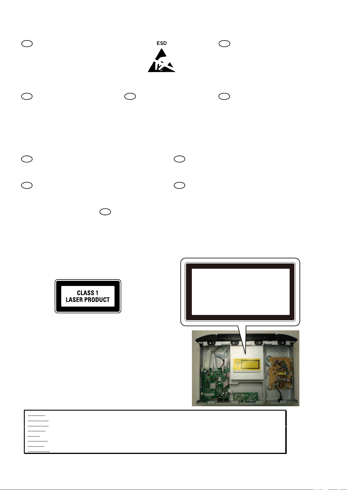
LASER SAFETY
This unit employs a laser. Only a qualified service person should
remove the cover or attempt to service this device, due to
possible eye injury.
I
AVVERTIMENTO
Tutti IC e parecchi semi-conduttori sono sensibili
alle scariche statiche (ESD).
La loro longevita potrebbe essere fortemente
in caso di non osservazione della piu grande
cauzione alla loro manipolazione.
Durante le riparazioni occorre quindi essere
collegato allo stesso potenziale che quello della
massa dell’apparecchio tramite un braccialetto a
resistenza.
Assicurarsi che i componenti e anche gli utensili
con quali si lavora siano anche a questo potenziale.
D
Bei jeder Reparatur sind die geltenden Sicherheitsvorschriften zu beachten.
Der Originalzustand des Gerats darf nicht verandert werden.
Fur Reparaturen sind Original-Ersatzteile zu verwenden.
I
Le norme di sicurezza esigono che l’apparecchio venga rimesso nelle
condizioni originali e che siano utilizzati pezzi di ricambiago idetici a quelli
specificati.
CAUTION-CLASS 2 VISIBLE AND INVISIBLE LASER
RADIATION WHEN OPEN. DO NOT STARE INTO THE BEAM.
VAROITUS-LUOKAN 2 NÄKYVÄÄ JA NÄKYMÄTÖNTÄ
LASERSÄTEILYÄ AVATUNA. ÄLÄ TUIJOTA SÄTEESEEN.
VARNING-KLASS 2 SYNLIG OCH OSYNLIG
LASERSTÅLNING VID ÖPPNING. STIRRA EJ NI I STRÅLEN.
ADVARSEL-KLASSE 2 SYNLIG OG USYNLIG LASERSTRÅLING
VED ÅBNING. SE IKKE IND I STRÅLEN.
USE OF CONTROLS OR ADJUSTMENTS OR PERFORMANCE
OF PROCEDURE OTHER THAN THOSE SPECIFIED HEREIN
MAY RESULT IN HAZARDOUS RADIATION EXPOSURE.
AVOID DIRECT EXPOSURE TO BEAM
WARNING
The use of optical instruments with this product will
increase eye hazard.
Repair handling should take place as much as possible with
a disc loaded inside the player
WARNING LOCATION: INSIDE ON LASER COVERSHIELD
CAUTION VISIBLE AND INVISIBLE LASER RADIATION WHEN OPEN AVOID EXPOSURE TO BEAM
ADVARSEL SYNLIG OG USYNLIG LASERSTRÅLING VED ÅBNING UNDGÅ UDS
ADVARSEL SYNLIG OG USYNLIG LASERSTRÅLING NÅR DEKSEL Å PNES UNNGÅ EKSPONERING FOR STRÅLEN
VARNING SYNLIG OCH OSYNLIG LASERSTRÅLNING NÄR DENNA DEL ÄR ÖPPNAD BETRAKTA EJ STRÅLEN
VARO! AVATT AESSA OLET ALTTIINA NÄKYVÄLLE JA NÄKYMÄTTÖMÄLLE LASER SÄTEILYLLE. ÄLÄ KATSO SÄTEESEEN
VORSICHT SICHTBARE UND UNSICHTBARE LASERSTRAHLUNG WENN ABDECKUNG GEÖFFNET NICHT DEM STRAHL AUSSETSEN
DANGER VISIBLE AND INVISIBLE LASER RADIATION WHEN OPEN AVOID DIRECT EXPOSURE TO BEAM
ATTENTION RAYONNEMENT LASER VISIBLE ET INVISIBLE EN CAS D'OUVERTURE EXPOSITION DANGEREUSE AU FAISCEAU
Æ
TTELSE FOR STRÅLING
6
Page 7
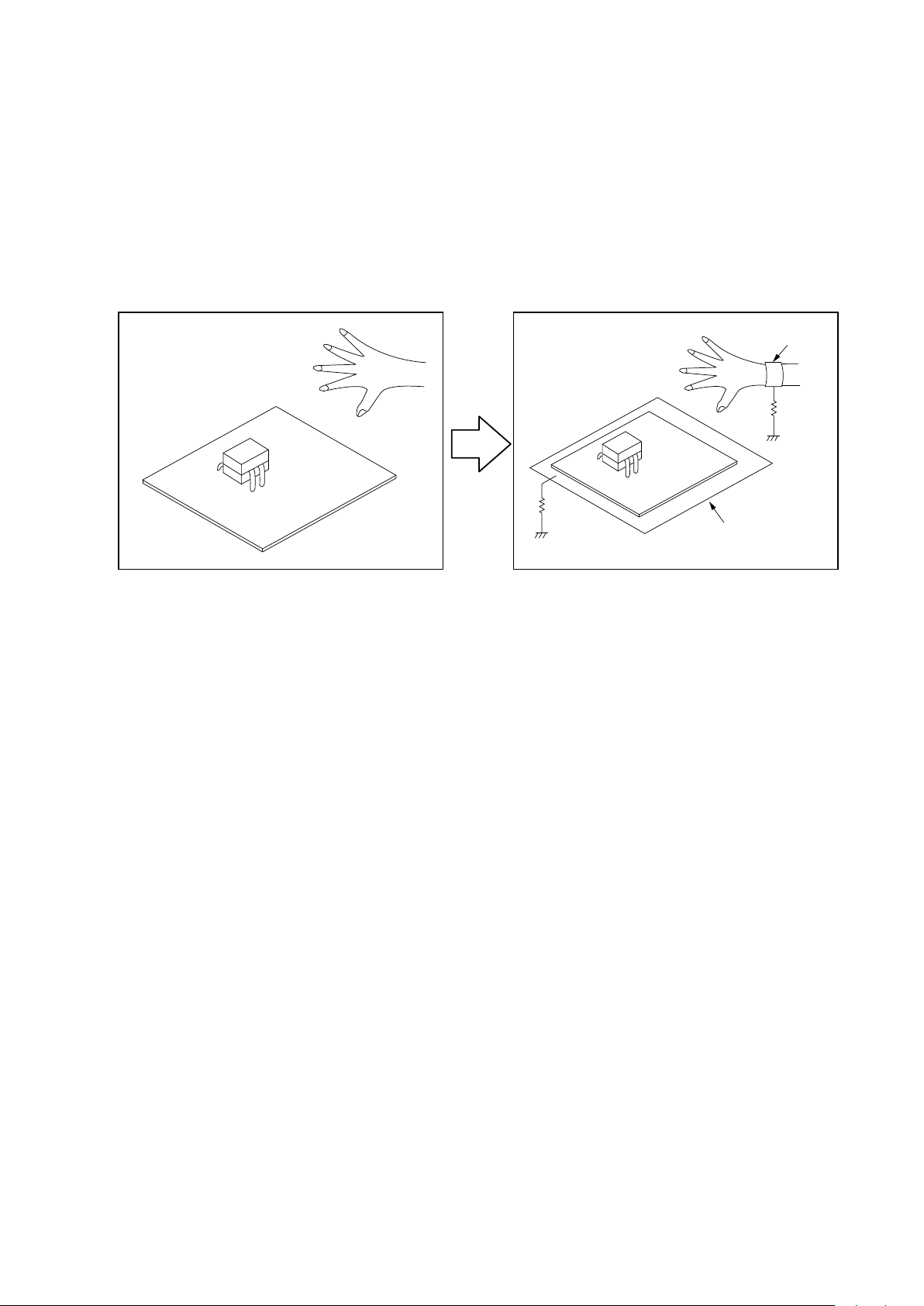
INSTRUCTIONS FOR HANDLING SEMI-CONDUCTORS AND OPTICAL UNIT
Electrostatic breakdown of the semi-conductors or optical pickup may occur due to a potential difference
caused by electrostatic charge during unpacking or repair work.
1. Ground for Human Body
Be sure to wear a grounding band (1 MΩ) that is properly grounded to remove any static electricity that may be charged on the body.
2. Ground for Workbench
Be sure to place a conductive sheet or copper plate with proper grounding (1 MΩ) on the workbench or other surface, where the
semi-conductors are to be placed. Because the static electricity charge on clothing will not escape through the body grounding band,
be careful to avoid contacting semi-conductors with your clothing
<Incorrect>
CBA
<Correct>
1MΩ
Grounding Band
1MΩ
CBA
Conductive Sheet or
Copper Plate
7
Page 8
TECHNICAL SPECIFICATIONS
Performance
n
Signal format : NTSC, PAL
Applicable discs /memory device :
(1) BD-Video disc :
12 cm, 1 side, 1 layer; 12 cm, 1 side, 2 layers
(2) DVD-Video / DVD-Audio disc :
12 cm, 1 side, 1 layer; 12 cm, 1 side, 2 layers /
12 cm, 2 sides, 2 layers (1 side, 1 layer)
8 cm, 1 side, 1 layer; 8 cm, 1 side, 2 layers /
8 cm, 2 sides, 2 layers (1 side, 1 layer)
(3) Super Audio CD :
12 cm, 1 layer / 12 cm, 2 layer / 12 cm, Hybrid
(4) Compact Disc (CD-DA) :
12 cm / 8 cm disc
(5) Memory device :
USB memory device (USB 2.0)
HDMI output :
Output terminal : 19-pin HDMI terminals, 1 set
(Deep Colour, Dolby Digital Plus, Dolby TrueHD, DTS-HD, 3D)
Analog audio output :
Output level : 2 Vrms (10 kΩ)
2 channels output terminal : Pin-jack, 1 set
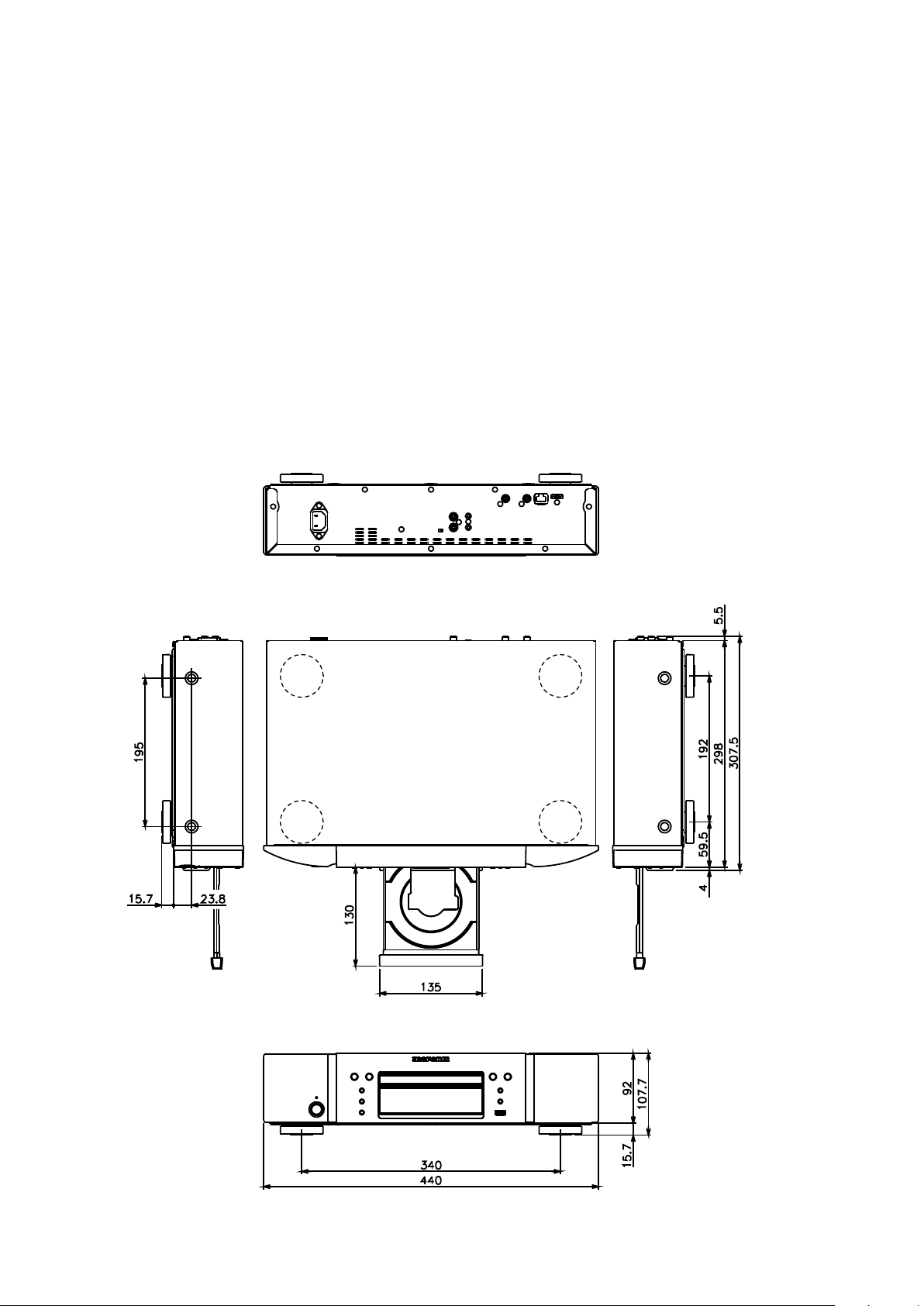
DIMENSION
Audio output characteristics :
(1) Frequency response
q BD (Linear PCM)
: 2Hz ~ 44kHz (96kHz sampling)
: 2Hz ~ 22kHz (48kHz sampling)
: 2Hz ~ 88kHz (192kHz sampling)
w DVD (Linear PCM)
: 2Hz ~ 44kHz (96kHz sampling)
: 2Hz ~ 22kHz (48kHz sampling)
: 2Hz ~ 88kHz (192kHz sampling)
e Super Audio CD
: 2Hz ~ 20kHz
r CD
(2) S/N ratio : 115dB (BD)
(3) Total harmonic distortion : 1kHz 0.0025% (BD)
(4) Dynamic range : 100dB (BD)
General
n
Power supply : AC 120 V, 60 Hz (for U)
AC 100 – 240 V, 50/60 Hz (for N, S)
AC 220 V, 50 Hz (for K)
Power consumption : 20W
0.3 W (Energy Saving Standby)
0.5 W (Normal Standby)
12 W (Quick Start)
: 2Hz ~ 40kHz
8
Page 9
CAUTIONS IN SERVICING
Initializing BD player
BD player initialization should be performed when the μcom, peripheral parts of μcom, and MAIN PCB. were replaced.
1. Turn on this model's power. "NO DISC" is displayed on the FL tube.
2. Press the this model's "1" and "9" buttons simultaneously. "INITIALIZING" is displayed on the FL tube.
3. The display on the FL tube switches to "INITIALIZED", the "NO DISC" display reappears and initialization is
completed.
NOTE : • If step 3 does not work, start over from step 1.
All user settings will be lost and this factory setting will be recovered after the set is initialized.
•
So make sure to note down your setting beforehand for restoring after the initialization.
91
ON/STANDBY (X)
Service tools
Measuring Disc: CD/TCD-784
DVD/VT502 or TDV-520A
BD/ABD-520 or BLX-108
Refer to "MEASURING METHOD AND WAVEFORMS".
z
When you repair the BD MECHA UNIT, you can use the following JIG.
Please order to Marantz Ofcial Service Distributor in your region if necessary.
Do not supply it : 232C (TTL) – USB conversion jig (Model: DUT-06635 by GeeeTech) : 1 Set
Part No. : 61205000300AS :
Refer to "HOW TO REPLACE THE MAIN PCB & BD MECHA OR BD MECHA".
z
4P RE-PH CONN CORD (1000mm) : 1 Set
9
Page 10
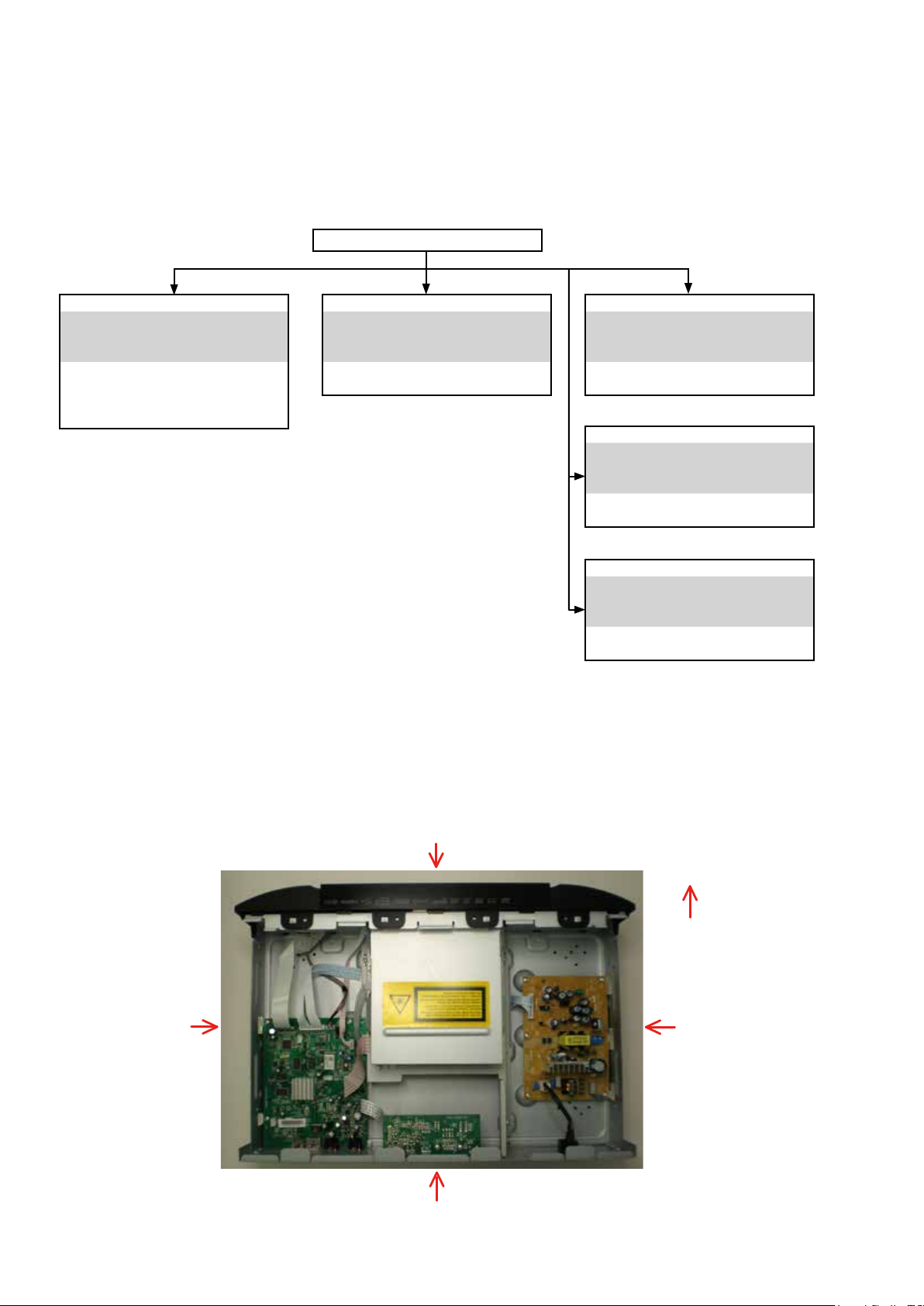
DISASSEMBLY
Shooting direction: C
• Disassemble in order of the arrow in the following gure.
• In the case of the re-assembling, assemble it in order of the reverse of the following ow.
• In the case of the re-assembling, observe "attention of assembling".
• If wire bundles are untied or moved to perform adjustment or replace parts etc., be sure to rearrange them neatly as
they were originally bundled or placed afterward.
Otherwise, incorrect arrangement can be a cause of noise generation.
TOP COVER
FRONT PANEL ASSY
Refer to "DISASSEMBLY
1. FRONT PANEL ASSY"
and "EXPLODED VIEW"
FRONT PANEL ASSY
(Ref. No. of EXPLODED VIEW : 1a)
DISPLAY PCB UNIT
(Ref. No. of EXPLODED VIEW : 13)
BD MECHA UNIT ASS'Y
Refer to "DISASSEMBLY
2. BD MECHA UNIT ASSY"
and "EXPLODED VIEW"
MAIN PCB UNIT ASSY
(Ref. No. of EXPLODED VIEW : 21)
MAIN PCB UNIT ASS'Y
Refer to "DISASSEMBLY
3. MAIN PCB UNIT ASSY"
and "EXPLODED VIEW"
MAIN PCB UNIT
(Ref. No. of EXPLODED VIEW : 21)
POWER PCB UNIT ASS'Y
Refer to "DISASSEMBLY
5. POWER PCB UNIT"
and "EXPLODED VIEW"
POWER PCB UNIT
(Ref. No. of EXPLODED VIEW : 20)
IR PCB UNIT ASS'Y
Refer to "DISASSEMBLY
4. IR PCB UNIT"
and "EXPLODED VIEW"
IR PCB UNIT
(Ref. No. of EXPLODED VIEW : 19)
About the photos used for "descriptions of the DISASSEMBLY" section
• The shooting direction of each photograph used herein is indicated on the left side of the respective photograph as
"Shooting direction: ***".
• Refer to the diagram below about the shooting direction of each photograph.
• Photographs with no shooting direction indicated were taken from the top of the set.
The viewpoint of each photograph
(Shooting direction)
[View from the top]
Shooting direction: B
Front side
Shooting direction: D
Shooting direction: A
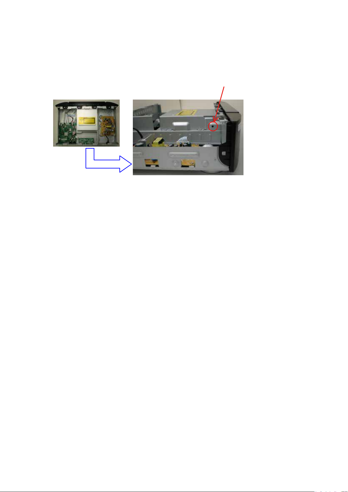
10
Page 11
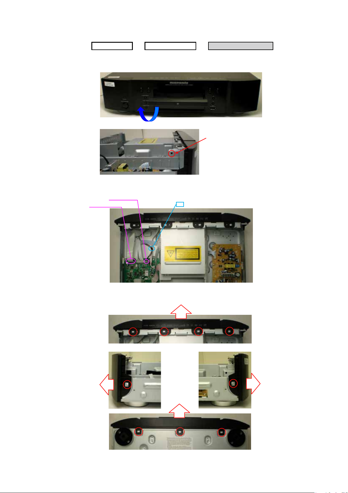
1. FRONT PANEL ASSY
Proceeding : TOP COVER
→
(1) Detach the LOADER PANEL.
Shooting direction: B
(2) Disconnect the connector wire and FFC.
4P-PH【XP3】
18P-FFC【XP4】
LOADER PANEL
cut
FRONT PANEL ASSY
→
Pressed in metal rod having a mechanism for
emergency open, stretched out like a small hole
on the left side of the clip to.
(3) Lift up to unhook the claw and move in the direction of arrow to gradually pull out the assembly.
Top side ×4, Side ×2 (Left and right), Bottom ×3
Top side
Shooting direction: C
Side
Bottom side
Shooting direction: D
11
Page 12
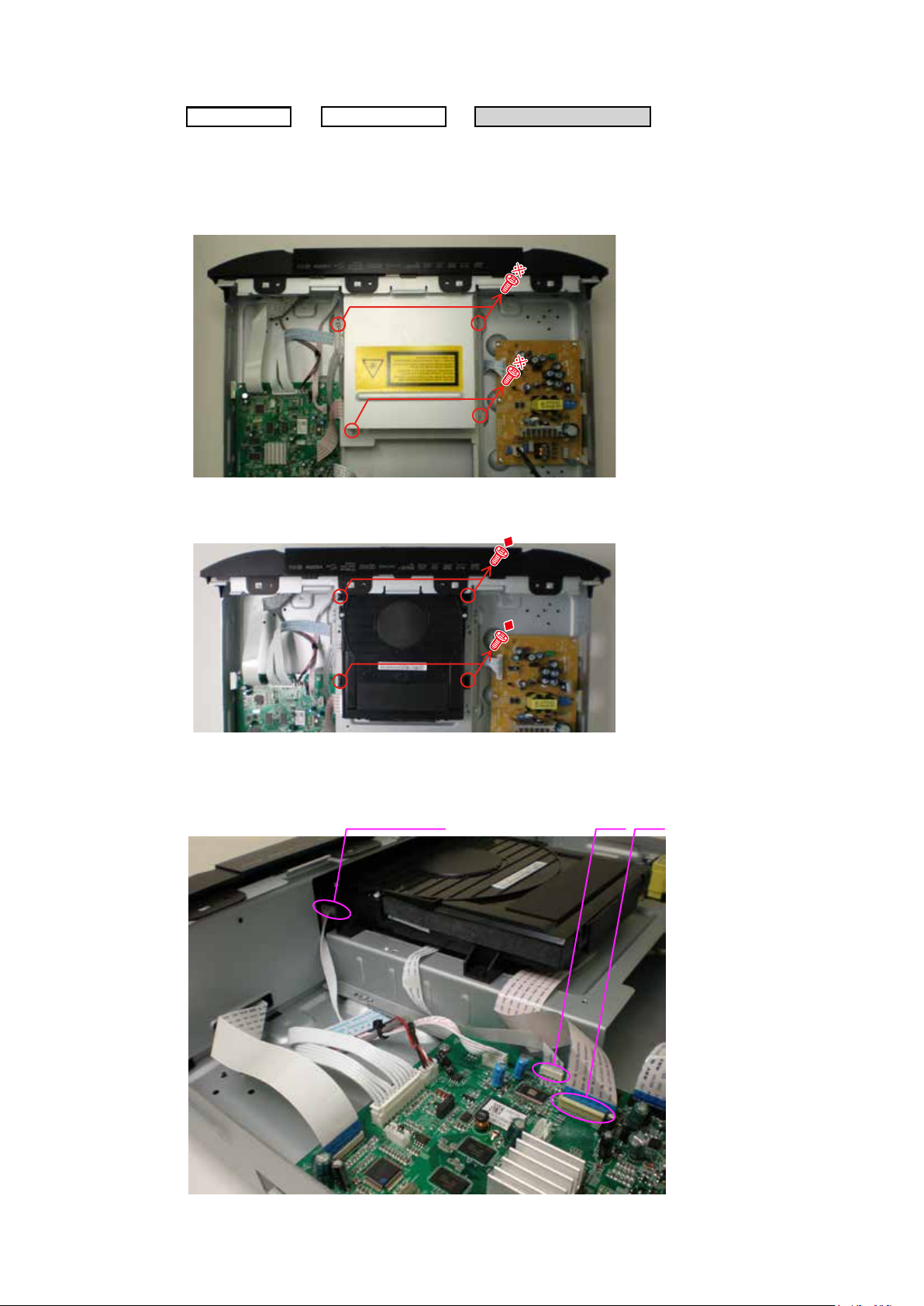
2. BD MECHA UNIT ASSY
Proceeding : TOP COVER
Please ensure ESD protection prior to handling the BD MECHA.
※
(1) Remove the screws.
Screw of Mecha cover ×4
(2) Remove the screws.
Screw of BD's Mecha ×4
MECHA COVER
→
BD MECHA UNIT ASSY
→
(3) Disconnect the connector wire and FFC.
45P-FFC【J2】, 9P-FFC【J4】
From the left side of the BD's Mecha, remove the screw.
【J2】【J4】【5P-PH CORD】
12
Page 13
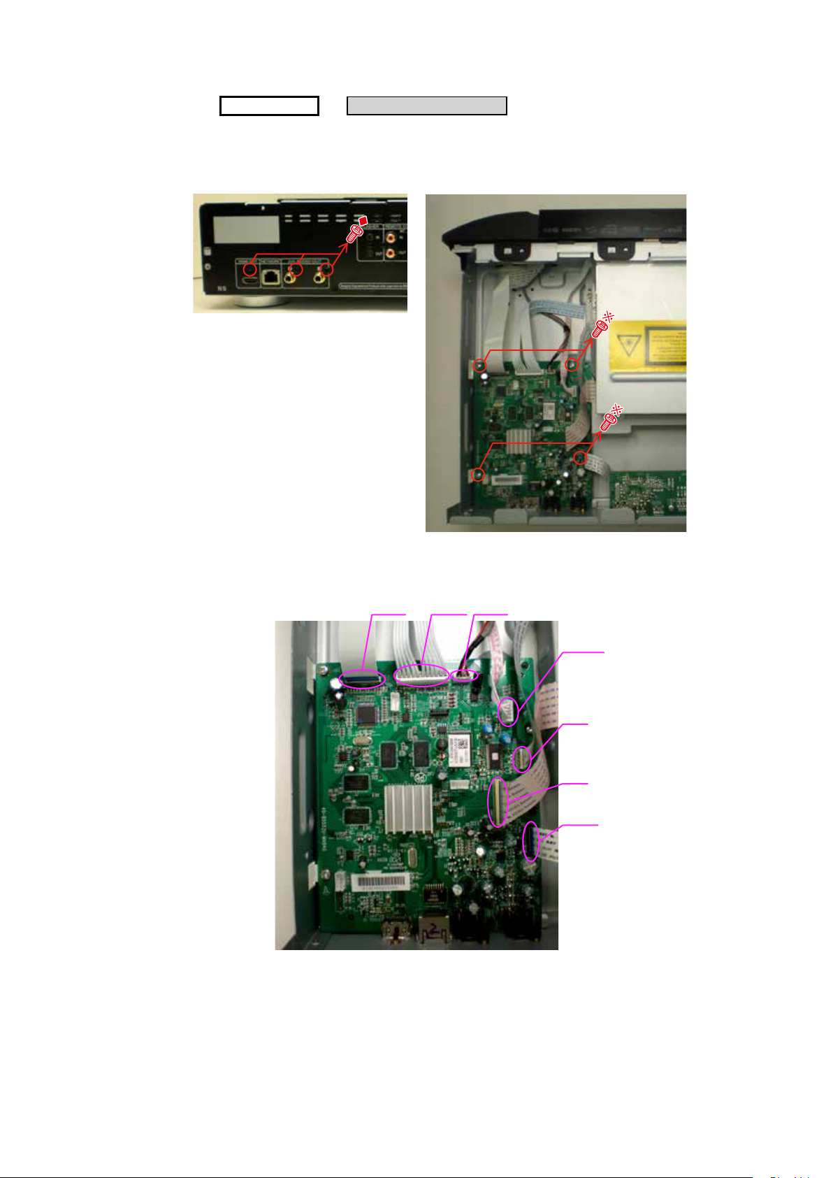
3. MAIN PCB UNIT ASSY
Proceeding : TOP COVER
(1) Remove the screws.
Remove the screws from REAR PANEL ×2
Remove the screws from TOP PANEL ×4
MAIN PCB UNIT ASSY
→
(2) Disconnect the connector wire and FFC.
Disconnect 13P-FFC【XP8】, 12P-PH【XP1
】
【XP4】 【XP1】【XP3】
【XP10】
【J4】
【J2】
【XP8】
13
Page 14
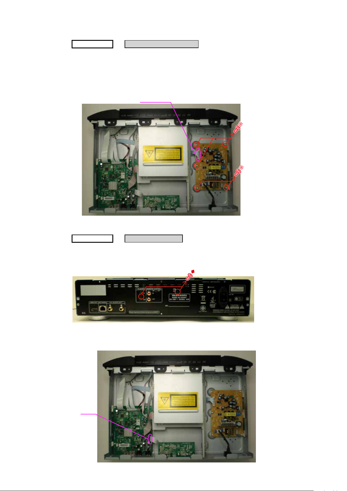
4. POWER PCB UNIT ASSY
Proceeding : TOP COVER
(1) Remove the screws.
Remove the screws from TOP ×5
(2) Disconnect the connector wire and FFC.
Disconnect 12P-PH【CN502/503】, 3P-VH【CN501
POWER PCB UNIT ASSY
→
】
【CN502/503】
5. IR PCB UNIT ASSY
Proceeding : TOP COVER
(1) Remove the screws.
Remove the screws from REAR PANEL ×2
(2) Disconnect the connector wire and FFC.
Disconnect 13P-FFC【XP8
→
】
IR PCB UNIT ASSY
【XP8】
14
Page 15
REMOVING DISCS
(1) Remove the Top Cover.
(2) Open the CD tray.
Shooting direction: D
Pressed in metal rod having
a mechanism for emergency
open, stretched out like a small
hole on the left side of the clip to.
15
Page 16
DIAGNOSTICS OF OPTICAL PICKUP
Make failure diagnostics of the Optical Pickup as follows.
If the laser drive current (Iop) becomes more than BD : ± 6 [mA], DVD or CD : ±12 [mA] of the initial value, the Optical
q
Pickup should be replaced.
The laser drive current initial value is checked by "Iop checked Method" of next page.
Load ve times of following disc again and playing it for one minute. It becomes the aim of the Optical Pickup
w
exchange when it cannot play.
BD-RE ABD-RE540W(made by ALMEDIO)
In case of replacing the Pickup, change the whole part of the MAIN PCB & BD MECHA or BD MECHA.
No mechanical adjustment is necessary after the replacement. (HOW TO REPLACE THE MAIN PCB & BD MECHA OR
BD MECHA (page 17))
Laser drive current initial value:
FL Display (The display part of 13 digits)
1 2 3 4 5 6 7 8 9 10 11 12 13
CD :
T 2 1 : m m m m : n n n n
FL Display (The display part of 13 digits)
DVD :
BD(SL) :
1 2 3 4 5 6 7 8 9 10 11 12 13
T 2 2 : m m m m : n n n n
FL Display (The display part of 13 digits)
1 2 3 4 5 6 7 8 9 10 11 12 13
T 2 3 : m m m m : n n n n
Check the laser drive current value
q
Disc no read, unsteady playback, etc.
Laser drive current (Iop) check.
Current value of the BD Iop is ±6[mA],
DVD or CD Iop is ±12[mA] or more the
initial value.
The MAIN PCB & BD MECHA
or the BD MECHA replacing.
Check the playability disc
w
Disc no read, unsteady playback, etc.
ABD-RE540W disc playability check
(Load ve times of following disc)
Disc cannot play.
The MAIN PCB & BD MECHA
or the BD MECHA replacing.
16
Page 17
1. Iop checked Method
Select the laser ON/OFF(CD/DVD/BD)mode of the test mode, and check the Iop value of CD laser, DVD laser or BD
laser. (Refer to "6. Test mode")
FL Display (The display part of 13 digits)
1 2 3 4 5 6 7 8 9 10 11 12 13
T 2 L a s e r O n O f f
Laser current check
Press the "8" or "9" button to display the laser current value, and then select [X].
Check the current value of Iop (nnnn)
FL Display (The display part of 13 digits)
1 2 3 4 5 6 7 8 9 10 11 12 13
T 2 X : m m m m : n n n n
(X=1 : CD laser mode, 2 : DVD laser mode, 3 : BD(SL) laser mode
(mmmm[mA] : Initial value, nnnn[mA] : Current value)
2. To clear the accumulated laser on time
Press the "1" button while the accumulated laser on time is displayed ("TC1, "TC2", "TC3" ) until "TC4*clear??"
appears at the display. If the "1" button is pressed, the accumulated laser on time of CD, DVD and BD is cleared
FL Display (The display part of 13 digits)
1 2 3 4 5 6 7 8 9 10 11 12 13
T C 4 * - - c l e a r ? ?
When "TC1", "TC2" or "TC3" is selected with the "8" or "9" button, "mmmmmm" is displayed as "0" so you can
check.
FL Display (The display part of 13 digits)
1 2 3 4 5 6 7 8 9 10 11 12 13
T C Y - - - m m m m m m h
(Y=1 : CD, 2 : DVD , 3 : BD, mmmmmm : Time)
17
Page 18

HOW TO REPLACE THE MAIN PCB & BD MECHA OR BD MECHA
NOTE: The optical pick-up laser diode (LD) is instantly degraded or damaged by static electricity or a power
surge. When handling the BD MECHA UNIT, always be sure to earth yourself, and use an earth mat on the
workbench and oor for grounding.
• BD MECHA UNIT Replacement Conditions
If the laser amperage (Iop) exceeds the stipulated range (see the laser on/off mode in test mode (page 25)), replace the
BD MECHA or replace the MAIN PCB & BD MECHA. If other problems occur, replace the MAIN PCB & BD MECHA.
Stipulated range: For BD, within ±6 [mA] of the initial value; for DVD/CD, within ±12 [mA] of the initial value.
• The following two parts are specied as service parts for the MECHA UNIT.
1. MAIN PCB & BD MECHA : (Part No. : 919304100210M)
2. BD MECHA : (Part No. : 919304100230S)
1. How to Replace the MAIN PCB & BD MECHA
(1) Refer to the removal procedure, and remove and replace the MAIN PCB & BD MECHA. (see "DISASSEMBLY")
(2) Follow the rmware update procedure, and update the rmware to the latest version.
(see "VERSION UPGRADE PROCEDURE OF FIRMWARE")
2. How to Replace the BD MECHA
2.1. Devices Used
1. PC
2. USB - 232C (TTL) conversion jig (Model: DUT-06635 by GeeeTech) (Do not supply)
3. 4P RE-PH CONN CORD (1000mm) (Part No. : 61205000300AS)
4. Write software (5.12.71(8550+KES470)_1Dscan.zip)
2.2. Replacement Overview
(1) Before replacing the UNIT, write all of the UNIT data of the unit to be replaced onto the set.
(2) After performing (1), replace the UNIT.
(3) Congure the settings for the set in which the UNIT was replaced.
2.3. Before replacing
[Preparation]
1. Set unit before replacing the UNIT
2. PC with write software (5.12.71(8550+KES470)_1Dscan.zip) installed
3. USB - 232C (TTL) conversion jig
4. UNIT for replacement
18
Page 19
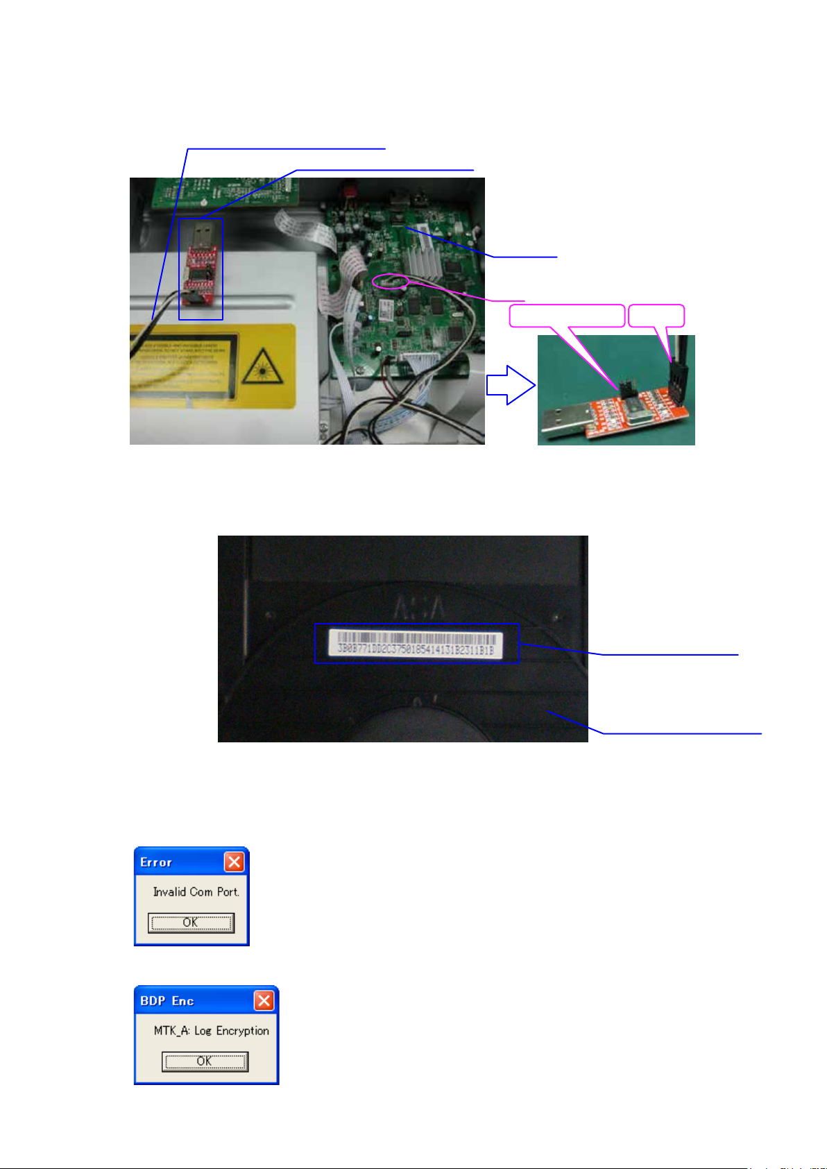
[Connection]
(1) Connect the 232C (TTL) side 4P PH connector of the USB - 232C (TTL) conversion jig to the MAIN PCB of the set.
(2) Connect the USB side of the USB - 232C (TTL) conversion jig to the PC.
4P RE-PH CONN CORD (1000mm)
USB - 232C(TTL) conversion jig
MAIN PCB
CON1
Jumper pin : 3.3V
[Writing new optical pick-up data ]
• Barcode position of optical pick-up unit
f mark
View from the top
(1) Switch on the power on of the set before the BD MECHA is replaced.
(2) Decompress the 5.12.71(8550+KES470)_1Dscan.zip folder and start the "Rpower.exe".
(3) A pop-up is displayed. Click "OK".
(4) Click "OK".
1Dimensional Bar Code
BD MECHA for replacement
19
Page 20
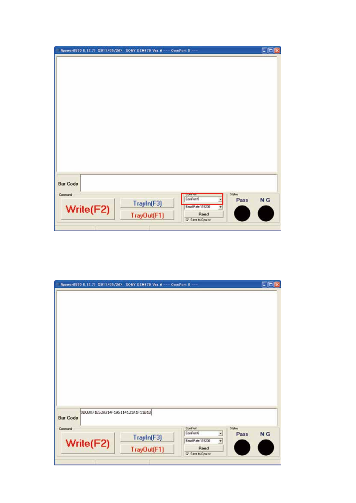
(5) On the screen below, select "ComPort XX".
Select the USB - 232C (TTL) conversion jig port.
(6) Enter the Bar Code BOX 32-digit hexadecimal number listed at the bottom of one-dimensional bar code
replacement for the BD MECHA.
One dimension of bar code data can stick to reading, Bar Code BOX in bar code leaders and can input.
NOTE: The bar code data of the optical pickup, please do not enter the wrong data. Please do not confused
with other data of the optical pickup also.
20
Page 21
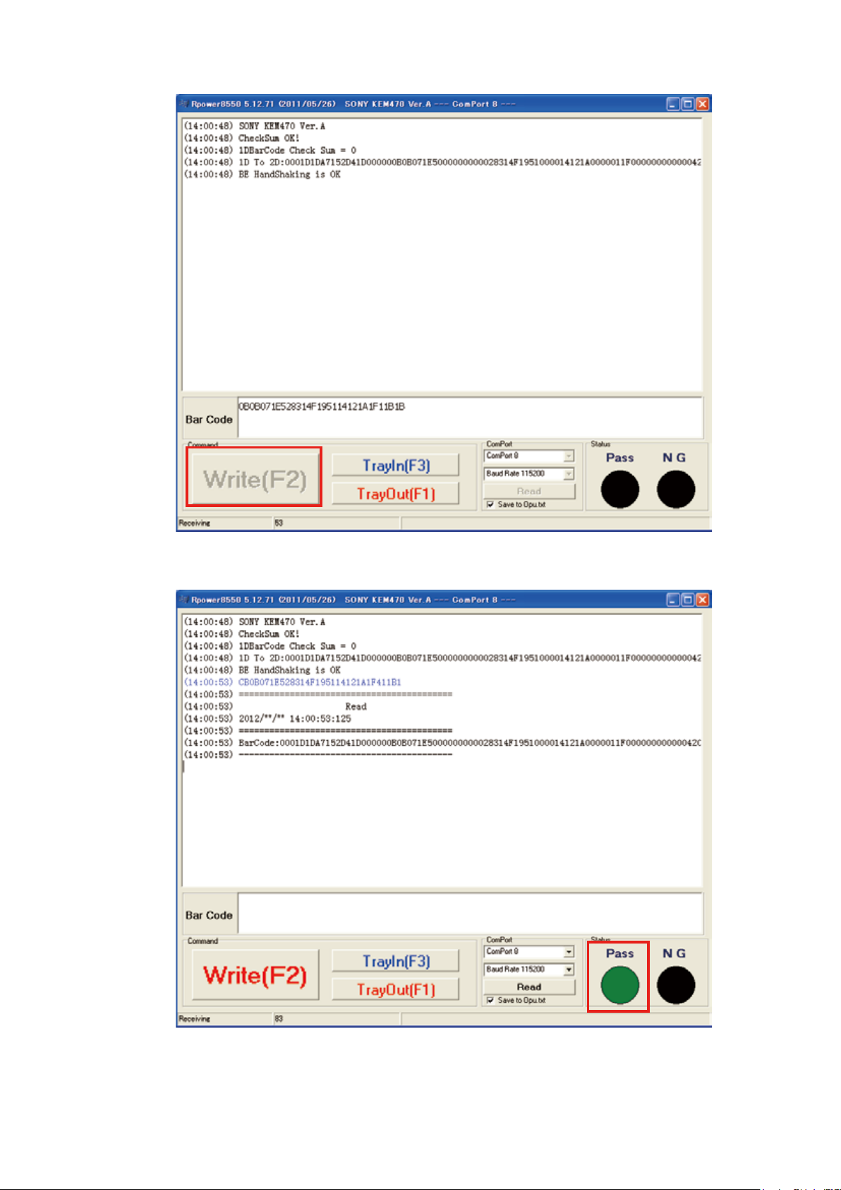
(7) Click Write(F2).
(8) When “Pass” changes to green, writing to the Flash ROM of the MAIN PCB is complete.
(9) Switch off the set unit power, and remove the 232C (TTL) side 4P PH connector of the USB - 232C (TTL)
conversion jig from the MAIN PCB (CON1).
21
Page 22
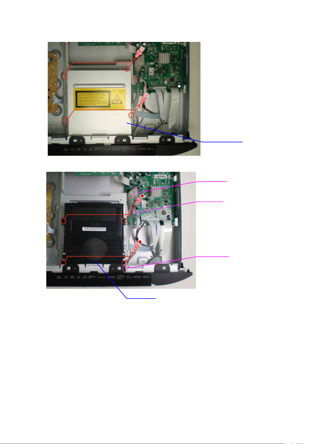
2.4. Replace the BD MECHA UNIT ASSY
(1) Remove the MECHA COVER.
MECHA COVER
(2) Move the optical pickup to the outer circumference, remove the FFC, and remove the screws.
J2 45P-FFC
J4 9P-FFC
5P-PH CORD
BD MECHA
(3) Attach the BD MECHA for replacement to the set unit. (When assembling the unit, perform the steps in reverse
order.)
(4) Check that the 45P-FFC, 9P-FFC and 5P-PH connector cords have been connected.
2.5. Congure the settings of the set that contains the new BD MECHA
(1) Check the laser amperage (see laser on/off mode in the test mode (page 25)).
Check that the values are ±6 [mA] from the initial value for BD, and ±12 [mA] from the initial value for DVD/CD.
(2) Clear the total laser usage time (see the procedure for clearing the accumulated laser on time in test mode (page
26)).
(3) Check BD, DVD, and CD media playback.
(4) If there are no problems with playback, remove the disc, press the "ON/STANDBY" button to switch to standby
status, and remove the AC plug from the AC socket.
(5) Attach the top cover, and this completes the replacement procedure.
22
Page 23
HOW TO REPLACE THE MAIN PCB UNIT ASSY
Service Part for the MAIN PCB UNIT ASSY
・
MAIN PCB: (Part No. :919639100340M)
s
1.1. Devices Used
(1) PC
(2) USB - 232C (TTL) conversion jig (Model: DUT-06635 by GeeeTech) (Do not supply)
(3) 4P RE-PH CONN CORD (1000mm) (Part No. : 61205000300AS)
(4) Write software (5.12.71(8550+KES470)_1Dscan.zip)
1.2. Replacement Overview
(1) Replace the MAIN PCB UNIT ASSY. (Disconnected J2 45P FFC)
(2) Writing Mecha's data to the replacement MAIN PCB UNIT.
(3) Turn off the unit, then connect 45P FFC of J2.
(4) To conrm the operation.
1.3. Before replacing
[Preparation]
(1) The unit of before replacement.
(2) Replacement MAIN PCB UNIT ASSY
(3) PC with write software (5.12.71(8550+KES470)_1Dscan.zip) installed
(4) USB - 232C (TTL) conversion jig
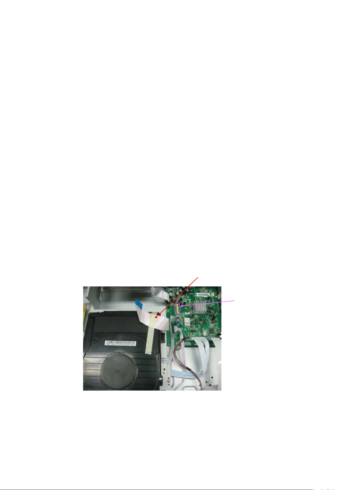
1.4. Replace the MAIN PCB UNIT ASSY
(1) Replacement MAIN PCB UNIT ASSY. (Refer to "DISASSEMBLY 3. MAIN PCB UNIT ASSY ")
(45P FFC J2 does not connect at this time.)
(2) Remove the MECHA COVER.
(3) Fixed to the MECHA UNIT to prevent short circuit. (J2 45P FFC)
J2 45P FFC
J2 45P FFC BASE
1.5. Connection and Writing optical pick-up data
(1) Refer to "HOW TO REPLACE THE MAIN PCB & BD MECHA OR BD MECHA,
[Connection] and [Writing new optical pick-up data ]"(P.19) , then writing new optical
pick-up data to MAIN PCB UNIT.
23
Page 24
1.6. Operation check
(1) Connect the 45P FFC of J2
J2 45P FFC
(2) Attach the MECHA COVER.
(3) Attach the TOP COVER.
(4) Follow the rmware update procedure, and update the rmware to the latest version.
(see "VERSION UPGRADE PROCEDURE OF FIRMWARE")
(5) Check the laser amperage (see laser on/off mode in the test mode (page 28)).
Check that the values are ±6 [mA] from the initial value for BD, and ±12 [mA] from the initial value for DVD/CD.
(6) Check BD, DVD, and CD media playback and operation.
(7) If there are no problems with playback, remove the disc, press the ON/STANDBY button to switch to standby
status,and remove the AC plug from the AC socket.
(8) Completes the replacement procedure.
Note: In the case of exchange, only MAIN PCB UNIT is cleared in the laser total use time.
24
Page 25

SERVICE MODE
Front-end version
1. Initial setting mode
1.1. preparation
(1) Equipment used: None
(2) Unit setting: No spec other than the following procedure.
1.2. procedure
Initialize the BD player when µcom, peripheral parts of µcom, or MAIN PCB. unit has been replaced in servicing.
b
All user setting will be lost and its factory setting will be restored when this initialization is made. Be sure to memorize
b
your setting for restoring again after the initialization.
(1) Turn on this model's power. "NO DISC" is displayed on the FL tube.
(2) Press the this model's "1" and "9" buttons simultaneously. "INITIALIZING" is displayed on the FL tube.
(3) The display on the FL tube switches to "INITIALIZED", the "NO DISC" display reappears and initialization is
completed.
2. Firmware version check mode
2.1. preparation
(1) Equipment used: None
(2) Unit setting: No spec other than the following procedure.
2.2. procedure
Front-end and Back-end and SYS com version check mode.
b
(1) Press the "SETUP" button on the remote controller to display the SETUP menu.
(2) Press remote controller "3265".
(3) The version is displayed on the TV screen as follows.
marantz
General Setting
System
Language
Ratings
Network
Others
Select
Factory Page
HQ 00003604,HF 00000000, MCU007
Version
JVM CDCA_JVM100311_2586
Loader: CV0017 8530
DVD Region Cod
BD Region Code
Reset Password
ENTER
Confirm
Reset
0
1
SETUP
Version
Version
Fmt buda
Fmt buda
Loader: 4Fxxxx
Exit
HQ 0000xxxx
MCUxxx
Back-end version
SYS com version
25
Page 26

3. Tray lock mode
3.1. preparation
(1) Equipment used: None
(2) Unit setting: No spec other than the following procedure.
3.2. procedure
[Setting]
(1) Pressing the "1" and "8" buttons for simultaneously, plug the AC cord into a power outlet.
(2) "TRAY LOCK" is displayed on the FL tube and tray opening/closing is invalidated.
[Cancel]
(1) Unplug this model's AC cord from the power outlet.
(2) Pressing the "1" and "8" buttons for simultaneously, plug the AC cord into a power outlet.
(3) "PLEASE WAIT" is displayed on the FL tube and tray opening/closing is enabled.
The tray lock mode is also canceled when the product is initialized.
b
4. Remote lock mode
4.1. preparation
(1) Equipment used: None
(2) Unit setting: No spec other than the following procedure.
4.2. procedure
[Setting]
(1) Pressing the
(2) “Lock-On” is displayed on the FL tube, and operations with the remote control and the REMOTE CONTROL input
terminal on the back of the UD5007 are disabled.
"PURE DIRECT" and "9" buttons for simultaneously.
[Cancel]
(1) Pressing the
(2) "Lock-Off" is displayed on the FL tube and remote lock mode is made canceled.
"PURE DIRECT" and "9" buttons for simultaneously.
5. All Lit / All Off mode for the FL tube
5.1. preparation
(1) Equipment used: None
(2) Unit setting: No spec other than the following procedure.
5.2. procedure
[Setting]
(1) Pressing the "PURE DIRECT" and "8" buttons for simultaneously, plug the AC cord into a power outlet.
If All Lit / All Off mode is set for the FL tube, the FL tube’s display area is fully lit.
(2) Press the "PURE DIRECT" button to ‘all off’ display.
[Cancel]
(1) Remove the power cable for 5 seconds or more to cancel All Lit / All Off mode for the FL tube.
26
Page 27

6. Test mode
6.1. Entering the test mode
The test mode is entered by pressing the "5" and "8" buttons simultaneously, plug the AC cord into a power outlet.
When the test mode is set, the "1" and "3" indicators light.
FL tube display when test mode entered
FL Display (The display part of 13 digits)
1 2 3 4 5 6 7 8 9 10 11 12 13
T E S T M O D E
When the test mode is set, the choice screen of the mode appears on the monitor.
6.2. Selecting the mode
The following modes are available.
・
(1) Laser on/off (CD/DVD/BD) mode : T2
(2) Error rate (skew) measurement mode : T7
(3) Accumulated laser on time display mode : TC
(4) Test mode cancel : TI
When the "9" button is pressed after entering the test mode, the display switches in the order: "T2, T7, TC, TI, T2
q
…"
FL Display (The display part of 13 digits)
1 2 3 4 5 6 7 8 9 10 11 12 13
T 2 L a s e r O n O f f
FL Display (The display part of 13 digits)
1 2 3 4 5 6 7 8 9 10 11 12 13
T 7 E r r o r R a t e
FL Display (The display part of 13 digits)
1 2 3 4 5 6 7 8 9 10 11 12 13
T C L a s e r O n T i m
FL Display (The display part of 13 digits)
1 2 3 4 5 6 7 8 9 10 11 12 13
T I T e s t E x i t
When the "8" button is pressed, the display switches in the opposite order from q above, starting from the
w
current position (for example, if currently at "TC", it switches as follows: "T7, T2 ").
27
Page 28

6.3. About each mode
With the mode selected, press the "1" button to set that mode.
・
(1) Laser on/off (CD/DVD/BD) mode
Press the "8" or "9" button to select [X] and press the "1" button to set it.
Laser on/off control is executed and the laser current is displayed.
FL Display (The display part of 13 digits)
1 2 3 4 5 6 7 8 9 10 11 12 13
T 2 X : m m m m : n n n n
(X=1 : CD laser mode, 2 : DVD laser mode, 3 : BD(SL) laser mode)
(mmmm[mA] : Stored data, nnnn[mA] : Current value)
When the current value is more that BD: ±6[mA], DVD or CD: ± 12[mA] of saved data, it becomes the pickup
b
transducer's target.
In this case, replace the mechanism unit.
When the "2" button is pressed, the layer above the current layer is displayed. See "6.4 Stopping the mode".
(2) Error rate measurement mode
Press the "8" or "9" button to select [YY] .
Refer to [Table 1 - Error rate details].
FL Display (The display part of 13 digits)
1 2 3 4 5 6 7 8 9 10 11 12 13
T Y Y F F F F F F F F F F
(YY : measurement mode, F : Address and error rate (When not set, "F" is displayed.)
Press the "1" button to begin error rate measurement. The address and error rate are displayed.
For a description of the displayed measurement results, see "Table 1: Error rate details".
FL Display (The display part of 13 digits)
1 2 3 4 5 6 7 8 9 10 11 12 13
T Y Y m m m m m m
(YY : selection mode [71 to 94], m : address [PBA][HEX], l : error rate [COUNT/SEC] [DEC])
(Note) CD (4x-speed) : Renewal of data is carried out for every 300 frame.
Error rate of 75 frames is displayed.
DVD (1.6x-speed) : Renewal of data is carried out for every 80ECC block.
Error rate of 8ECC block is displayed.
BD (1.6x-speed) : Renewal of data is carried out for every 136LDC clusters block.
Error rate of 8LDC clusters block is displayed.
The mode chosen when selection mode was changed into the trace execution and the "1" button was pressed is
performed from the beginning.
When the "1" button is pressed without changing selection mode, the mode under selection is performed from the
beginning.
(If the "1" button is pressed, the address corresponding to the chosen mode will be searched again.)
The pause mode is set after tracing is completed.
When the "2" button is pressed, the layer above the current layer is displayed. See "6.4 Stopping the mode".
l l l l
28
Page 29

(3) Accumulated laser on time display mode
Press the "8" or "9" button to select [Y] and press the "1" button to set it.
The accumulated laser on time is displayed.
FL Display (The display part of 13 digits)
1 2 3 4 5 6 7 8 9 10 11 12 13
T C Y m m m m m m h
(Y=1 : CD, 2 : DVD , 3 : BD, mmmmmm : Time(Fractions of hours are counted up one hour on the display.)
When the "2" button is pressed, the layer above the current layer is displayed. See "6.4 Stopping the mode".
---To clear the accumulated laser on time---
Press the "1" button while the accumulated laser on time is displayed ("TC1, "TC2", "TC3" ) until "TC4*clear??"
appears at the display.
FL Display (The display part of 13 digits)
1 2 3 4 5 6 7 8 9 10 11 12 13
T C 4 * c l e a r ? ?
If the "1" button is pressed, the accumulated laser on time of CD, DVD and BD is cleared.
FL Display (The display part of 13 digits)
1 2 3 4 5 6 7 8 9 10 11 12 13
T C 1 0 h
When "TC1", "TC2" or "TC3" is selected with the "8" or "9" button, "mmmmmm" is displayed as "0" so you
can check.
(4) Test mode cancel
A conrmation message is displayed. Press the "1" button to set, canceling the test mode.
FL Display (The display part of 13 digits)
1 2 3 4 5 6 7 8 9 10 11 12 13
T I 1 R e a l l y ?
When the "2" button is pressed, the layer above the current layer is displayed. See "6.4 Stopping the mode".
29
Page 30

6.4. Stopping the mode
When the "2" button is pressed, the layer above the current layer is displayed. The relationship between the different
modes and the display of the different layers is shown on the table below.
Mode 1 layer 2 layer 3 layer
Laser on/off (CD/DVD/BD) mode T2 LaserOnOff T2X mmmm nnnn Non
Error rate measurement mode T7 Error Rate TYYFFFFFFFFFF TYYmmmmmmllll
Accumulated laser on time display mode TC LaserOnTim TCY mmmmmmh TC4* clear??
Test mode cancel TI Test Exit TI1 Really? Non
6.5. About the OPEN/CLOSE (
) button
5
Even during the test mode, the tray is opened and closed when the "5" button is pressed.
6.6. Test mode detailed table
Table 1: Error rate details
Measurement
YY
71 The inner
72 The inner
73 The inner
74 The inner
75 The central
76 The central
77 The central
78 The central
79 The outer
80 The outer
81 The outer
82 The outer
83 The inner
position
circumference of
1-layer
circumference of
1-layer
circumference of
1-layer
circumference of
1-layer
circumference of
1-layer
circumference of
1-layer
circumference of
1-layer
circumference of
1-layer
circumference of
1-layer
circumference of
1-layer
circumference of
1-layer
circumference of
1-layer
circumference of
2-layer
BIS error detection
signed number
It is invalid. It is invalid. It is invalid. When this is selected for BD, DVD or
LDC error detection
signed number
It is invalid. It is invalid. C2 uncorrectable
BIS error detection
signed number
It is invalid. It is invalid. It is invalid. When this is selected for BD, DVD or
LDC error detection
signed number
It is invalid. It is invalid. C2 uncorrectable
BIS error detection
signed number
It is invalid. It is invalid. It is invalid. When this is selected for BD, DVD or
LDC error detection
signed number
It is invalid. It is invalid. C2 uncorrectable
BIS error detection
signed number
Error rate display details for each media type
BD DVD CD
It is invalid. It is invalid. When this is selected for DVD or CD,
PI error detection
number
It is invalid. It is invalid. When this is selected for DVD or CD,
PI error detection
number
It is invalid. It is invalid. When this is selected for DVD or CD,
PI error detection
number
It is invalid. It is invalid. When this is selected for DVD or CD,
C1 error
detection number
error number
C1 error
detection number
error number
C1 error
detection number
error number
Remarks
T71 FFFFFFFFFF display.
CD, T72 FFFFFFFFFF display.
When this is selected for BD or DVD,
T74 FFFFFFFFFF display.
T75 FFFFFFFFFF display.
CD, T76 FFFFFFFFFF display.
When this is selected for BD or DVD,
T78 FFFFFFFFFF display.
T79 FFFFFFFFFF display.
CD, T80 FFFFFFFFFF display.
When this is selected for BD or DVD,
T82 FFFFFFFFFF display.
T83 FFFFFFFFFF display.
30
Page 31

Measurement
YY
84 The inner
85 The inner
86 The inner
87 The central
88 The central
89 The central
90 The central
91 The outer
92 The outer
93 The outer
94 The outer
position
circumference of
2-layer
circumference of
2-layer
circumference of
2-layer
circumference of
2-layer
circumference of
2-layer
circumference of
2-layer
circumference of
2-layer
circumference of
1-layer
circumference of
1-layer
circumference of
1-layer
circumference of
1-layer
It is invalid. It is invalid. It is invalid. When this is selected for BD, DVD or
LDC error detection
signed number
It is invalid. It is invalid. It is invalid. When this is selected for BD, DVD or
BIS error detection
signed number
It is invalid. It is invalid. It is invalid. When this is selected for BD, DVD or
LDC error detection
signed number
It is invalid. It is invalid. It is invalid. When this is selected for BD, DVD or
BIS error detection
signed number
It is invalid. It is invalid. It is invalid. When this is selected for BD, DVD or
LDC error detection
signed number
It is invalid. It is invalid. It is invalid. When this is selected for BD, DVD or
Error rate display details for each media type
BD DVD CD
PI error detection
number
It is invalid. It is invalid. When this is selected for DVD or CD,
PI error detection
number
It is invalid. It is invalid. When this is selected for DVD or CD,
PI error detection
number
It is invalid. When this is selected for 1-layer DVD
It is invalid. When this is selected for DVD 1-layer
It is invalid. When this is selected for DVD 1-layer
Remarks
CD, T84 FFFFFFFFFF display.
or CD, T85 FFFFFFFFFF display.
CD, T86 FFFFFFFFFF display.
T87 FFFFFFFFFF display.
CD, T88 FFFFFFFFFF display.
or CD, T89 FFFFFFFFFF display.
CD, T90 FFFFFFFFFF display.
T91 FFFFFFFFFF display.
CD, T92 FFFFFFFFFF display.
or CD, T93 FFFFFFFFFF display.
CD, T94 FFFFFFFFFF display.
* The inner circumference of the layer refers to the physical inner circumference for DVD parallel, the physical outer
circumference for the opposite case.
* The inner circumference of the layer refers to the physical outer circumference for DVD parallel, the physical inner
circumference for the opposite case.
31
Page 32

PROCEDURE FIRMWARE FOR UPGRADING THE VERSION OF THE FIRMWARE
You can update by downloading the latest version from the Internet.
1. Update from the Internet
1.1. preparation
(1) System requirements
• Internet Connection by Broadband Circuit
• Modem
• Router
• Ethernet cable (CAT-5 or greater recommended)
(2) Setting
Internet
Computer
Router
Modem
To WAN port
To LAN port
To LAN port
NET WORK
connector
LAN port/Ethernet connector
1.2. Checking and updating the rmware
Check if the latest rmware exists. You can also check approximately time required to complete an update.
(1) Press the "SETUP" button on the remote control to display the GUI menu.
(2) Use the cursor buttons to select "General Setting" → "System" → "Firmware Update" → "Update check".
(3) Press the "ENTER" button.
• If the rmware on the website is latest, proceed to (4) Press "Enter" Button.
• If the latest rmware has been already installed, press the "RETURN" button to return to SETUP menu.
(4) Press the "ENTER" button.
• When updating is completed, return to normal status about 20 seconds later.
--- Cautions on Firmware Update ---
• In order to update the rmware, you must have the correct system requirements and settings for a broadband Internet
connection.
• Do not turn off the power until updating is completed.
• Once updating starts, normal operations on this unit cannot be performed until updating is completed. Also, setting
items of the GUI menu of this unit or setting items of the image adjustment may be initialized.
Note down of the settings before updating, and set them again after updating.
32
Page 33

TROUBLE SHOOTING
1. Power (Power Board)
1. Power does not turn on.
Power does not turn on.
POWER_LED is not blinking red. Refer to "2. LED blinking".
Yes
Is the fuse of F501 normal?
Yes
Check 5VSTB(CN502#1).
Is output voltage about 5.2V?
Yes
Check PCON(CN502#2).
Is input voltage about 2V?
Yes
Check +5V(CN502#3).
Is outut voltage about 5.1V?
Yes
Check +12VA(CN502#9).
Is output voltage about +12V?
Yes
Check -12VA(CN502#11).
Is ouput about -12V?
Yes
Check +12VM(CN502#7).
Is output about +12V?
Yes
No
No
No
No
No
No
No
No
Check abnormalities of the circuit of a primary side.
(Such as D501,D502,D503,D504,Ce501,Q501,U501)
Defect parts should be exchanged.
After-repair Hughes is exchanged.
Refer to "3. Power board".
Check abnormalities of the connection circuit of
PCON. (Such as Q506)
Defect parts should be exchanged.
When there are no abnormalities in a POWER board,
MAIN PCB can be exchanged.
Check abnormalities of the connection circuit of +5V.
(Such as Q512,Q505)
Defect parts should be exchanged.
When there are no abnormalities in a POWER board,
MAIN PCB can be exchanged.
Check abnormalities of the connection circuit of +12V.
(Such as D511,Q510,Q509,Q508,Q507,ZD503)
Defect parts should be exchanged.
When there are no abnormalities in a POWER board,
MAIN PCB can be exchanged.
Check abnormalities of the connection circuit of -12V.
(Such as D512,Q511,ZD504,U512)
Defect parts should be exchanged.
When there are no abnormalities in a POWER board,
MAIN PCB can be exchanged.
Check abnormalities of the connection circuit of +12V.
(Such as Q507,Q508)
Defect parts should be exchanged.
When there are no abnormalities in a POWER board,
MAIN PCB can be exchanged.
Abnormality of the board for MAIN, replace the MAIN
PCB.
33
Page 34

2. LED blinking
POWER_LED is blinking red.
PC0N (CN502#2) and +5V (CN502#3) are measured
simultaneously.
Before PCON is set to "L", +5V has not carried out
voltage drops.
Yes
PC0N (CN502#2) and +12VA (CN502#9) are
measured simultaneously.
Before PCON is set to "L", +5V has not carried out
voltage drops.
Yes
Abnormality of the board for MAIN, replace the MAIN
board.
3. Power board
No output +5VSTB(CN502#1).
No
No
Check abnormalities of the connection circuit of +5V.
(Such as Q512,Q505)
Defect parts should be exchanged.
When there are no abnormalities in a POWER board,
MAIN PCB can be exchanged.
Check abnormalities of the connection circuit of +12V.
(Such as D511,Q510,Q509,Q508,Q507,ZD503)
Defect parts should be exchanged.
When there are no abnormalities in a POWER board,
MAIN PCB can be exchanged.
Where CN502 is removed, 5VSTB (CN502#1) is not
outputted.
Yes
There are no abnormalities in the connection circuit of
+5VSTB.
(Such as D509,U503,U502,U505,L550)
Yes
Check abnormalities of the circuit of a primary side.
(Such as D501,D502,D503,D504,Ce501,Q501,U501)
Defect parts should be exchanged.
No
No
Abnormality of the board for MAIN, replace the MAIN
board
Abnormality of the board for MAIN, replace the MAIN
board
34
Page 35

4. DISPLAY (Display Board)
FL TUBE doesn't light.
Does not appear when press the "DIMMER" on the
remote control.
Yes
CHeck VFD_RST(U2#9).
Is voltage more than 2.6V ?
Yes
Is VH(U2#6) set to the 29V~35V?
Yes
Check Between F-(U2#52) and F+(U2#1) .
Is voltage 3.78V~4.62V?
No
No
No
No
May be DIMMER was working.
Also, May be "PURE DIRECT" was working.
To replace the parts to check there is nothing wrong
with the connection circuit VFD_RST. (Such as a cable
of Q19, Q17, XP4, XP4) Abnormal when there is no
substrate to replace the MAIN PCB.
To replace the parts to check there is nothing wrong
with the circuit connection of VH. Such as cable, XP4
(ZD602, D609, Q16, U1, +12 V, XP4
Yes
Check F-(U2#52).
Is voltage 2.0V~3.0V?
Yes
Chek VDD(U2#7).
Is voltage 3.0V~3.6V?
Yes
Check the output signal to VSTB(U2#10),
VCLK(U211), VDATA(U2#12).
Is voltage set to "H"(more than 2.6V)
Yes
No
No
No
To replace the parts to check there is nothing wrong
with the connection circuit F +, of F-. Such as cable,
XP4 (U700, D610, D611, D612, +12 V, XP4
To replace the parts to check there is nothing wrong
with the connection circuit of VDD. (Such as a cable
of XP4, XP4)Abnormal when there is no substrate to
replace the MAIN PCB.
(U2 # 10), VCLK (U211), to replace the parts to check
there is nothing wrong with the connection circuit (U2
# 12) VDATA VSTB. (Such as a cable of XP4, XP4)
Abnormal when there is no substrate to replace the
MAIN PCB.
VFD and (U2), abnormality of the peripheral circuits.
Check the location of the abnormality, and correct it.
35
Page 36

5. HDMI
No picture or sound is output.
Is the set in "PURE DIRECT MODE" "Off"?
Yes
Is a contact part of HDMI JACK J1 normal?
Is there no damage around the contact where HDMI
cable are inserted?
Are there no bad soldering?
Yes
Is that the cable correctly inserted into the connector
XP1 11p of Main PCB?
Yes
Is that supplied from 5V 3pin of XP1 of Main PCB?
Yes
Replace Main PCB.
No
Set the "PURE DIRECT MODE" "Off".
No
Replace the HDMI JACK.
No
To be inserted into the XP1 the "11p" cable
No
Refer to 2.LED blinking.
6. Network
Cannot connect to Internet
Is there nothing wrong with the ETHER JACK P1 of
Main PCB?
Is there no damage around the contact where
Ethernet cable are inserted.
Are there no bad solder joints?
Yes
Is that the cable correctly inserted into the connector
XP1 11p of Main PCB?
Yes
Is that is supplied from 5V 3pin of XP1 of Main PCB?
Yes
No
Replace the ETHER JACK.
No
To be inserted into the XP1 the 11p cable.
No
Refer to 2.LED blinking.
Replace Main PCB.
36
Page 37

7. USB
Does not recognize the USB.
Is there nothing wrong with the USB connector P1 of
the Display PCB?
Is there no damage around the contact where USB
cable are inserted.
Are there no bad solder joints?
Yes
No
Replace the F.PANEL ASSY
Is there is nothing wrong with the 4P cable JP1 of
Display PCB?
Does disconnection of the cable?
Are there bad solder joints?
Yes
Is the cable correctly inserted into the connector 4P
XP3 of Main PCB?
Yes
Is that supplied from 5V 3pin of XP1 of Main PCB?
Yes
Replace Main PCB.
8. No Audio output
There is no output from the (2P RCA) ANALOG
output.
No
Replace the F.PANEL ASSY
No
4p cable to be inserted into the XP3.
No
Refer to No.2 LED blinking.
Terminal P2 pin jack on the Main PCB (or P3, P4)
There is nothing wrong with the. Not bad, abnormal
soldering or the like.
Yes
Is 11p cable inserted properly to XP1 of Main PCB?
Yes
Does XP1 of Main PCB(#9:+12 V, #11:-12V) supply
voltage?
Yes
Replace Main PCB.
No
No
No
37
Replace the RCA PIN JACK.
11p cable to be inserted into the XP1.
Refer to Power Board
No.2 LED blinking.
Page 38

9. Disc playback error
Disc playback error
Is 45P FFC inserted properly to J2 of Main PCB? 45P FFC inserted into the J2.
Yes
Is 9P FFC inserted properly to J4 of Main PCB? 9P FFC inserted into J4.
Yes
Is 5P PH connector inserted properly to X10 of Main
PCB?
Yes
Is that 12V supplied from the XP10 7pin of Main PCB
No
No
No
No
5P PH connector to be inserted into theX10.
Refer to 1.Power Board
Check +12VM(CN502#7). Is it output about +12V?
Yes
Is that output of 8V from 2pin of U17 Main PCB?
Yes
Refer to "HOW TO REPLACE THE MAIN PCB &BD
MECHA OR BD MECHA"
No
Replace Main PCB.
38
Page 39

BLOCK DIAGRAM
A
4 4
B
P2
R
L
RCA
Audio AMP&LPF
NJM4565
AUDIO DAC
+12VA
-12V
AUDIO_5V
L
FOR UD5007
C
+5V_STBY
R
HDMI_5V
NJM2882
HDMI OUTPUT
HDMI
PESD_TPD4S010B
PM1781
J1
D
Ethernet
LFE8634
P1
E
OUT
IN
W.remote
OUT
IN
IR SWITCH BOARD
100-240V 50/60Hz
POWER AC IN
RC5
FOR UD5007
W.remote
1.1V
1.5V
3.3V
IIS
IIS
3
IIC
MCU
CS8966
MCU_3.3V
G9091-330T11U
MT8555/DPBG
J2
45PIN*0.5
3.3V
DVD LOADER
2 2
ASA F-9829D1+Cover + SONY470AAB
J3
9PIN*1.0
AA+
BB+
GND
W
V
U
COMMON
LOADLOAD+
GND
TRAYIN#
XP4
4PIN*2.0
+12V
VCC
MOTER
DRIVER
TI2050G4
1 914
VCC
A3.3V
G556B1
8Gb
N FLASH
VCC
USB_5V
1 4
XP2 USB
4PIN*2.0
1Gbit
DDR3
1Gbit
DDR3
1Gbit
DDR3
1Gbit
DDR3
1.5V
18PIN*1.0
XP3
18
EEPROM
POWER_K
3.3V
1.5V
1.1V
AUDIO_5V
3.3V LDO
G966A-25ADJ
DC-DC
EUP3485
DC-DC
AT1526
78L05
1
+5V_STBY
5V
12V
XP1
11PIN*2.5
11
NCP1271
POWER
SUPPLY
1
+5V_STBY
PS_ON#
5V
5V
GND
GND
+12V
GND
+12VA
GND
-12V
1
XS201
11PIN*2.5
11
3
MAIN BOARD(MP1)
1
1 1
A
GREEN RED
ON / STANDBY
PURE DIRECT
B
VFD
VFD WITH DRIVER IC
SPI
(Futaba:014BT102GINK)
IR
38kHz
C
3.3V
GND
KEY_IN_A
KEY_IN_B
STANDBY_KEY
MCU_LED_CTRL_1
MCU_LED_CTRL_2
VSTB
VCLK
+12V
VDATA
+5V_STBY
PLAY STOP
OPEN/CLOSE
DISPLAY
D
VFD_RST
IR_IN
W_REMOTE
18
16PIN*2.0MM
PREV
BOARD
NEXT
XS304 4PIN*2.0
USB
USB
BOARD
E
39
Page 40

POWER BLOCK DIAGRAM
+12VM
(U501)
NCP1271
PCON
PCON
(U512)
L79L12ACZ
+12VA
-12VA
+5VSTB
MAIN
BOARD
+5V(VCC
40
PCON
(U503)
TL431
PCON
STANDBY ON/OFF
Page 41

PRINTED WIRING BOARDS
181716151413121110987654321
MAIN
(COMPONENT SIDE)
MAIN
(FOIL SIDE)
A
B
C
D
E
F
G
H
I
J
K
鉛フリー半田
半田付けには、鉛フリー半田 (Sn-Ag-Cu) を使用してください。
Lead-free Solder
When soldering, use the Lead-free Solder (Sn-Ag-Cu).
L
M
41
Page 42

FRONT
(COMPONENT SIDE)
181716151413121110987654321
A
B
C
D
E
PWD1G
(COMPONENT SIDE)
F
G
H
I
J
42
鉛フリー半田
半田付けには、鉛フリー半田 (Sn-Ag-Cu) を使用してください。
Lead-free Solder
When soldering, use the Lead-free Solder (Sn-Ag-Cu).
K
L
M
Page 43

FRONT
(FOIL SIDE)
181716151413121110987654321
A
B
C
D
E
PWDG1
(FOIL SIDE)
F
G
H
I
J
鉛フリー半田
半田付けには、鉛フリー半田 (Sn-Ag-Cu) を使用してください。
Lead-free Solder
When soldering, use the Lead-free Solder (Sn-Ag-Cu).
K
L
M
43
Page 44

181716151413121110987654321
IRA1G
(COMPONENT SIDE)
USE1G
(COMPONENT SIDE)
IRA1G
(FOIL SIDE)
USE1G
(FOIL SIDE)
A
B
C
D
E
F
G
H
I
J
K
L
44
鉛フリー半田
半田付けには、鉛フリー半田 (Sn-Ag-Cu) を使用してください。
Lead-free Solder
When soldering, use the Lead-free Solder (Sn-Ag-Cu).
M
Page 45

87654321
+12VA/0.1A
CE560
CE560
+
+
470uF/16V
470uF/16V
+12VM
R573NCR573
NC
0.1uF/50V/X7R
0.1uF/50V/X7R
MAIN
BOARD
1
2
3
4
5
6
7
8
9
10
11
12
12PIN/2.5mm
12PIN/2.5mm
R572NCR572
NC
0.1uF/50V/X7R
0.1uF/50V/X7R
C557
C557
01 +5VSTB
02 PCON
03 +5V
04 +5V
05 GND
06 GND
07 +12VM
08 GND
09 +12VA
10 GND
11 -12VA
12 GND
+12VA
C559
C559
+12VM/0.5A
+5VSTB
PCON
+5V
+12VM
+12VA
-12VA
CN503
CN503
7PIN/2.5mm
7PIN/2.5mm
1
2
3
4
5
6
7
1
2
3
4
CN504
CN504
4PIN/2.5mm
4PIN/2.5mm
1
2
3
4
5
6
7
1
2
3
4
Upper model
01 +5VSTB
02 PCON
03 +5V
04 +5V
05 GND
06 GND
07 +12VM
01 +12VA
02 GND
03 -12VA
04 GND
A
B
C
D
L552 3.3uH/3AL552 3.3uH/3A
CY503
CY503
470pF/250VAC
470pF/250VAC
11
10
10
12
8
D509
D509
10A60V
10A60V
9
U502
U502
R5271KR527
JP507NCJP507
NC
D511
D511
SR3100/3A/100V
SR3100/3A/100V
D512 FR107/1A/1000VD512 FR107/1A/1000V
C550
C550
2200pF/50V/X7R
2200pF/50V/X7R
R55022R550
22
+
+
CE550
CE550
1500uF/16V
1500uF/16V
R551
R551
470
470
R552
R552
2.2K
2.2K
3
U503
U503
1
H431
H431
2
+M12V
ZD505
ZD505
BZX79C15
BZX79C15
1K
R56222R562
22
C555
C555
1000pF/1KV
1000pF/1KV
L550 3.3uH/3AL550 3.3uH/3A
CE551
CE551
1500uF/16V
1500uF/16V
+
+
C551
C551
0.1uF/50V/X7R
0.1uF/50V/X7R
R576NCR576
-12VA
BZX79C15
BZX79C15
ZD506
ZD506
CE555
CE555
+
+
1000UF/25V
1000UF/25V
CE558
CE558
+
+
220uF/25V
220uF/25V
NC
CE561
CE561
+
+
1000UF/25V
1000UF/25V
R569
R569
100K
100K
Q511
Q511
NPN_MMBT8050C
NPN_MMBT8050C
+
+
CE552
CE552
1000uF/16V
1000uF/16V
R553
R553
10K
10K
R555
R555
11.3K/1%
11.3K/1%
R563 10KR563 10K
R554
R554
12.1K/1%
12.1K/1%
R565
2.2K
2.2K
Q509
Q509
NPN_3DG3904M
NPN_3DG3904M
R570 2.2KR570 2.2K
R571 0R571 0
0.1uF/50V/X7R
0.1uF/50V/X7R
R556
R556
10K
10K
Q505
Q505
NPN_3DG3904M
NPN_3DG3904M
R557 1KR557 1K
Q506
Q506
NPN_3DG3904M
NPN_3DG3904M
R558
R558
10K
10K
C556 2200pF/50V/X7RC556 2200pF/50V/X7R
ZD504 20HSCZD504 20HSC
U512 L79L12ACZU512 L79L12ACZ
2
VIN
+5VSTB
C561
C561
D510
D510
MBRX140/40V/1A
MBRX140/40V/1A
R559 4.7KR559 4.7K
C552
C552
0.1uF/50V/X7R
0.1uF/50V/X7R
Q508
Q508
PNP_3CG3906M
PNP_3CG3906M
R566 2.2KR566 2.2K
Q510
Q510
NPN_3DG3904M
NPN_3DG3904M
VOUT
GND
1
R564
R564
10K
10K
12-S
L553 7.5mmL553 7.5mm
3
CE559
CE559
+
+
100uF/16V
100uF/16V
Q512
Q512
P_PMK35EP
P_PMK35EP
1
2
3
4
C560 1uF/63VC560 1uF/63V
PCON
Q507 P_AP6679GIQ507 P_AP6679GI
DS
G
C562
C562
1uF//50V/X7R
1uF//50V/X7R
+12VA
-12VA
R574NCR574
C558
C558
NC
0.1uF/50V/X7R
0.1uF/50V/X7R
8
7
6
5
CE554
CE554
470uF/16V
470uF/16V
+
+
R560
R560
22K
22K
R561
R561
10K
10K
+M12V
ZD503
ZD503
BZX79C11
BZX79C11
R567
R567
150
150
R568
R568
200
200
-12VA/0.1A
+5V
C554
C554
0.1uF/50V/X7R
0.1uF/50V/X7RR518
R575NCR575
NC
12-S
C553
C553
0.1uF/50V/X7R
0.1uF/50V/X7R
L551 3.3uH/3AL551 3.3uH/3A
CE557
CE557R565
CE556
CE556
+
+
+
+
470uF/16V
470uF/16V
1000uF/16V
1000uF/16V
1
+5VSTB
2
PCON
+5V/2.5A
+12VM
+12VA
-12VA
3
4
5
6
7
8
9
10
11
12
CN502
CN502
CY505NCCY505
NC
D504
D504
D503
D503
RL207/2A/1000V
RL207/2A/1000V
RL207/2A/1000V
D501
D501
RL207/2A/1000V
RL207/2A/1000V
R503 NCR503 NC
R501 NCR501 NC
CX501 0.1uF/275VACCX501 0.1uF/275VAC
CX502 NCCX502 NC
CY501
CY501
100pF/250VAC
100pF/250VAC
RV501 VDR/470VRV501 VDR/470V
F501
F501
FUSE_T2AL/250V
FUSE_T2AL/250V
CN501
CN501
2PIN/7.92mm
2PIN/7.92mm
90-264VAC&50/60Hz INPUT
RL207/2A/1000V
RL207/2A/1000V
RL207/2A/1000V
LF501
LF501
30mH
30mH
112
D502
D502
optional
2
0.1uF/275VAC
0.1uF/275VAC
R504 NCR504 NC
R502 NCR502 NC
C501
C501
CY502
CY502
470pF/250VAC
470pF/250VAC
TR501
TR501
NTC/10ohm
NTC/10ohm
CY506NCCY506
NC
CE501
CE501
+
+
100uF/450V
100uF/450V
U501
U501
NCP1271
NCP1271
latch
C505
C505
0.1uF/50V/X7R
0.1uF/50V/X7R
C507
C507
0.01uF/50V/X7R
0.01uF/50V/X7R
R520 NCR520 NC
R514
R514
51K
R515
R515
51K
VCC
6NC7HV8
RT1COMP2CS3GND
C506
C506
100pF/50V/NP0
100pF/50V/NP0
R518
12K
12K
R521 NCR521 NC
R508 47R508 47
D506
D506
MBRX140/40V/1A
MBRX140/40V/1A
R509 150R509 150
OUT5VCC
C504
C504
0.1uF/50V/X7R
0.1uF/50V/X7R
4
R517 100R517 100
JP502 0JP502 0
JP501 0JP501 0
CE503
CE503
22uF/50V
22uF/50V
R510
R510
10K
10K
+
+
R506NCR506
NC
ZD508
ZD508
BZX79C18
BZX79C18
NC
C503
C503
0.0022uF(222)400V
0.0022uF(222)400V
G
Q502NCQ502
Q503
Q503
NC
NC
R519 100R519 100
R5050R505
0
FB501
FB501
10mm
10mm
DS
Q501
Q501
N_SMK0465F
N_SMK0465F
1
R50711R5071
1
R50721R5072
R516 1KR516 1K
R522NCR522
NC
D508NCD508
NC
1
R50731R5073
1
R50741R5074
NC
C508NCC508
D505
D505
ZD507
ZD507
P6KE160A
P6KE160A
FR207/2A/1000V
FR207/2A/1000V
C509
C509
10pF/1KV
10pF/1KV
D507 FR107/1A/1000VD507 FR107/1A/1000V
CE502
CE502
+
+
22uF/50V
22uF/50V
R5231KR523
1K
PNP_MMBT8550CLT1
PNP_MMBT8550CLT1
VCC
VCC
Q504
Q504
latch
470pF/250VAC
470pF/250VAC
C502NCC502
NC
T501
T501
6
2
4
1
5
0.82mH
0.82mH
43
R5241KR524
R525
R525
43
1K
100
100
CY504
CY504
12
PS2561L1
PS2561L1
OVP
+5VSTB
ZD502
ZD502
BZX79C5V6
BZX79C5V6
R52610R526
10
12
U505
U505
PS2561L1
PS2561L1
45
STANDBY POWER
SCHEMATIC DIAGRAMS (1/15)
POWER
E
F
Page 46

+5V_STBY
+12V
3.3V
VFD_RST1
IR_IN
W_REMOTE
VDATA
VCLK
VSTB
STANDBY_KEY
KEY_IN_A
KEY_IN_B
MCU_LED_CTRL_1
MCU_LED_CTRL_2
FL_LINK_LED_CTRL
18P_ FFC_1.0mm
18P_ FFC_1.0mm
XP4
XP4
1
1
2
2
3
3
4
4
5
5
6
6
7
7
8
8
9
9
10
10
11
11
12
12
13
13
14
14
15
15
16
16
17
17
18
18
+12V
KEY_IN_A
KEY_IN_B
STANDBY_KEY
KEY_IN_A
KEY_IN_B
STANDBY_KEY
R6175R61
R53 75R53 75
87654321
+5V_STBY +5V_STBY
3.3V 3.3V
75
R51 12K/1%R51 12K/1%R52 2.2K/1%R52 2.2K/1%
0
R10R1
0
R20R2
0
R30R3
0
R60R6
IR_INIR_IN
+5V_STBY
10K/NC
10K/NC
R18
R18
IR_IN
C15
C15
0.1uF/50V/Y5V/NC
0.1uF/50V/Y5V/NC
R9733R97
Q18
Q18
DTA114EUA
DTA114EUA
33
100uF/16V
100uF/16V
IRM_12mm
IRM_12mm
2
1 3
CE5
CE5
+
+
C11
C11
0.1uF/50V/Y5V
0.1uF/50V/Y5V
1
IR
2
GND
3
VCC
4
GND
5
GND
IR1
IR1
IR TX module
D2D2
R96
R96
R62 NCR62 NC
360
360
W_REMOTE
C16
C16
0.01uF/50V/Y5V
0.01uF/50V/Y5V
A
FL_LINK_LED_CTRL
KEY_IN_A
KEY_IN_B
MCU_LED_CTRL_1
MCU_LED_CTRL_2
+5V_STBY
MCU_LED_CTRL_1
R58
C210
C210
100pF/50V/NP0
100pF/50V/NP0
NPN_3DG3904M
NPN_3DG3904M
1KR58 1K
R59
R59
10K
10K
C200 100pF/50V/NP0C200 100pF/50V/NP0
R42NCR42
NC
Q12
Q12
C199
C199
C209
C209
100pF/50V/NP0
100pF/50V/NP0
100pF/50V/NP0
100pF/50V/NP0
R43
R43
3.3K
3.3K
R44
R44
10K
10K
Q25
Q25
PNP_3CG3906M
PNP_3CG3906M
R45
R45
4.7K
4.7K
LED1
LED1
LED_RED+GREEN
LED_RED+GREEN
STANDBY_KEY
C201
C201
100pF/50V/NP0
100pF/50V/NP0
PNP_3CG3906M
PNP_3CG3906M
123
+5V_STBY
R120
R120
5.6K
5.6K
VFD_RST
VCLK
VSTB
VDATA
R54
R54
18K
18K
Q26
Q26
R121
R121
6.8K
6.8K
C198
C198
100pF/50V/NP0
100pF/50V/NP0
R46NCR46
NC
R47
R47
100K
100K
R55
R55
100K
100K
Q5
Q5
NPN_3DG3904M
NPN_3DG3904M
R67 1KR67 1K
R68
R68
10K
10K
C195 100pF/50V/NP0C195 100pF/50V/NP0
C197
C197
C196
C196
100pF/50V/NP0
100pF/50V/NP0
100pF/50V/NP0
100pF/50V/NP0
MCU_LED_CTRL_2
C513
C513
0.1uF/25V/X7R
0.1uF/25V/X7R
CE2
CE2
47uF/16V
47uF/16V
+
+
R86 NC/15KR86 NC/15K
VFD_RST1
R83
R83
NC/22K
NC/22K
Q13
Q13
NC/NPN_3DG3904M
NC/NPN_3DG3904M
C13
C13
NC/1000pF/50V/X7R
NC/1000pF/50V/X7R
R70 1KR70 1K
10K
10K
R69
R69
Q14
Q14
NC/NPN_3DG3904M
NC/NPN_3DG3904M
PWM
R84
R84
NC/1K
NC/1K
R85
R85
NC/1K
NC/1K
3.3V
R71
R71
10K
10K
R72 1KR72 1K
Q17
Q17
NPN_3DG3904M
NPN_3DG3904M
R71147R711
R71247R712
C10
C10
+
0.1uF/50V/Y5V
0.1uF/50V/Y5V
47uF/16V CE3+47uF/16V CE3
47
47
Q19
Q19
NPN_3DG3904M
NPN_3DG3904M
V12V
5
6DA7
8
TS
VCC
GND1TG2OUT3RESET
OUT
OUT
ADJ
R98 75/1%R98 75/1%
R99
R99
330
330
CV
4
V12V
PWM
C9
C9
1000pF/50V/X7R
1000pF/50V/X7R
2
4
3.3V
R601KR60
1K
C14
C14
0.01uF/50V/Y5V
0.01uF/50V/Y5V
VFD_RST
C8
C8
1000pF/50V/X7R
1000pF/50V/X7R
C7
C7
R50 2KR50 2K
R56 0R56 0
0.1uF/25V/X7R
0.1uF/25V/X7R
100pF/50V/NP0
100pF/50V/NP0
U1
SA555U1SA555
3
IN
1
U22
U22
AS1117
AS1117
D1
1N4148D11N4148
C514
C514
L601
L601
680uH/300mA
680uH/300mA
+
+
CE4
CE4
10uF/50V
10uF/50V
R102NCR102
NC
R48 10R48 10
R49 10R49 10
R101NCR101
NC
F+
F-
D610
D610
1N4007/1A/1000V
1N4007/1A/1000V
D611
D611
1N4007/1A/1000V
1N4007/1A/1000V
D612
D612
1N4007/1A/1000V
1N4007/1A/1000V
ZD602
ZD602
BZX79C33
BZX79C33
R138
R138
10K/1/4W
10K/1/4W
32V
R139
R139
10K/1/4W
10K/1/4W
D609
D609
1N4148
1N4148
Q16
Q16
NPN_S8050C
NPN_S8050C
6.5V
3.3V 3.3V
R12
R10
R10
10K
10K
VCLK VSTB
R6310R63
32V
R6510R65
3.3V
C19
C19
0.1uF/50V/Y5V
0.1uF/50V/Y5V
R12
10K
10K
VDATA
C18
C18
0.1uF/50V/Y5V
0.1uF/50V/Y5V
R6410R64
10
10
10
39K
39K
R66
R66
VSTB
VCLK
VDATA
3.3V
R14
R14
10K
10K
U2
VFD_RST
1
F+
3
DL
4
LGND
5
PGND
6
VH
7
VDD
8
OSC
9
REST
10
CS
11
CP
12
DA
13
TSA
14
TSB
39
NC
40
NC
41
NC
42
NC
43
NC
44
NC
45
NC
46
NC
47
NC
48
1G
49
Q1G
52
F-
FUTABAU2FUTABA
F+
1G
Q1G
F-
B
C
D
32V
Q20
R75
R75
100K
100K
R76
R76
33K
33K
Q20
NPN_3DG3904M
NPN_3DG3904M
1G
Q1G
R74 100R74 100
FL_LINK_LED_CTRL
R124 1KR124 1K
R125
R125
10K
10K
Q30
Q30
3904M
3904M
LED5LED5
RED LED
3.3V
R81 3.3KR81 3.3K
+12V
R80
R80
22K
22K
R77 1KR77 1K
100
100
Q21
R16
R16
R791KR79
1K
Q21
NPN_3DG3904M
NPN_3DG3904M
32V
R7833R78
33
Q22
Q22
NPN_3DG3904M
NPN_3DG3904M
E
STANDBY POWER
SCHEMATIC DIAGRAMS (2/15)
DISPLAY_01
46
F
Page 47

KEY_IN_A
KEY_IN_B
STANDBY_KEY
KEY_IN_A
KEY_IN_B
STANDBY_KEY
87654321
A
B
Marantz
KEY_IN_A
ESD3
ESD3
NC/ESD_8KV
NC/ESD_8KV
C204
C204
0.01uF/50V/Y5V
0.01uF/50V/Y5V
4PIN/2.0mm/200mm
4PIN/2.0mm/200mm
JP1
JP1
KEY_IN_B
ESD4
R34
R34
R37
6.8K/1%
6.8K/1%
R37
15K/1%
15K/1%
39K/1%
39K/1%
K3
D616
D616
OPENK3OPEN
1N4148
1N4148
SOUND MODEK2SOUND MODE
USBM1
USBP1
ESD2
ESD2
ESD1
ESD1
NC/ESD_8KV
NC/ESD_8KV
R113
R113
R114
R114
0/1%
0/1%
2.49k/1%
2.49k/1%
K9
K1
K2
RESOLUTIONK9RESOLUTION
PURE DIRECTK1PURE DIRECT
4
4
3
3
2
2
1
1
NC/ESD_8KV
NC/ESD_8KV
R38
R38
K8
0.1uF/50V/Y5V
0.1uF/50V/Y5V
ESD4
NC/ESD_8KV
NC/ESD_8KV
D617
D617
PLAYK8PLAY
1N4148
1N4148
C17
C17
0.01uF/50V/Y5V
0.01uF/50V/Y5V
VCC_USB
CE6
CE6
+
+
100uF/16V
100uF/16V
C205
C205
STANDBY_KEY
FB1
FB1
600
600
K4
R119
R119
2.5k/1%
2.5k/1%
R36
R36
R35
R35
R390R39
6.8K/1%
6.8K/1%
15K/1%
15K/1%
K5
PREVK5PREV
STOPK4STOP
P1
P1
0
K6
K10
K10
NEXTK6NEXT
PAUSE
PAUSE
USB-A/BK
USB-A/BK
6
1
VCC
Shell B
D-
D+
GND
Shell A
5
VCC_USB
2
USBM1
3
USBP1
4
GND
ESD5
ESD5
NC/ESD_8KV
NC/ESD_8KV
STANDBY_KEY
C206
C206
0.1uF/16V/Y5V
0.1uF/16V/Y5V
K7
ON/STANDBYK7ON/STANDBY
C
D
47
SCHEMATIC DIAGRAMS (3/15)
DISPLAY_02
E
F
Page 48

IN
GND
OUT
JK1
JK1
MINI-JACK
MINI-JACK
87654321
+5V_STBY
R750R75
0
R77
R77
R78NCR78
0/NC
0/NC
NC
C407
C406 NCC406 NC
0.01uF/50V/Y5VC407 0.01uF/50V/Y5V
A
R760R76
0
W_REMOTE
6
FB3 120FB3 120
6
5
FB15 120FB15 120
5
1
1
TP2TP2
3
FB5 120FB5 120
3
4
4
2
FB11 120FB11 120
2
TP3TP3
FG9
TP1TP1
D1
RB521SD1RB521S
TP4TP4
D2
BAV16WD2BAV16W
0.1uF/50V/X7R
0.1uF/50V/X7R
C398
C398
D3
BAV16WD3BAV16W
C399
C399
0.1uF/50V/X7R
0.1uF/50V/X7R
C403
C403
C402NCC402
C401
C401
C400
C400
C404
C404
1000pF/50V/X7R
1000pF/50V/X7R
220pF/50V/NP0
220pF/50V/NP0
NC
220pF/50V/NP0
220pF/50V/NP0
0.1uF/50V/X7R
0.1uF/50V/X7R
BZX79C6V2
BZX79C6V2
ZD1
ZD1
+5V_NSW_232C
R711KR71
1K
R72
R72
3.3K
3.3K
1
Q1
Q1
KTC3875S
KTC3875S
SOT-23
SOT-23
R73
R73
3.3K
3.3K
2 3
23
Q2
R74
R74
10K
10K
KRA104SQ2KRA104S
TP5TP5
C405NCC405
NC
1
FG9
DB9 female/nc
DB9 female/nc
FG9
Q13
Q13
PNP_3CG3906M/NC
PNP_3CG3906M/NC
FB8
FB8
500/800mA/NC
500/800mA/NC
R82 0/NCR82 0/NC
C10
C10
0.1uF/25V/Y5V/NC
0.1uF/25V/Y5V/NC
CE7
CE7
+
+
47uF/16V/NC
47uF/16V/NC
GND_REN0
Q18
Q18
NPN_3DG3904M/NC
NPN_3DG3904M/NC
R157
R157
GND
R158 10K/NCR158 10K/NC
10K/NC
10K/NC
FB9 120/200mA/NCFB9 120/200mA/NC
FB10 120/200mA/NCFB10 120/200mA/NC
0/NC
0/NC
R79
R79
RS323C_OUT
RS232C_IN
UD5007X
UD5007X(for North America)
UD5007X(for Europe)
UD5007X(for Russia)
UD5007X(for Asia)
UD5007X(for China)
UD5007X(for Japan)
AMX_POWER
W405
0.01uF/50V
C200
C200
C408
C408
1000pF/50V/X7R/NC
1000pF/50V/X7R/NC
C409
C409
0.1uF/50V
FG9
MCU_SET5 MCU_SET1 MCU_SET2 MCU_SET3 MCU_SET4
R313
NC
NC
NC
NC 10K 10K
NC
NC
W405
1
2
3
4
M3-SITE
M3-SITE
R309
10K
10K
10K NC
10K
R310 R311
NC
NC
10K
NC
NC NC
NC
10K
10K 10K
NC NC
STANDBY POWER
R312
10K
NC
K01K01K01
TP10TP10
C410
C410
0.1uF
0.1uF
C411
C411
0.01uF
TP9TP9
TP7TP7
1000pF/50V/X7R/NC
1000pF/50V/X7R/NC
C412NCC412
C413NCC413
GND
5
1
2
3
GND
4
3
IN
OUT
2
AV2-8.4-9/PB/nc
AV2-8.4-9/PB/nc
RCA2-4-2
RCA2-4-2
FB13
FB13
120
120
R7047R70
47
GND
0.01uF
R80
R80
0/NC
0/NC
NC
NC
C414
C414
1000pF/50V/X7R/NC
1000pF/50V/X7R/NC
C198
C198
0.1uF/25V/Y5V
0.1uF/25V/Y5V
TP13TP13
C199
C199
0.1uF/25V/X7R
0.1uF/25V/X7R
GND
C415
C415
TP11TP11
R81
R81
0/NC
0/NC
FB6 120/200mA/NCFB6 120/200mA/NC
FB7 120/200mA/NCFB7 120/200mA/NC
ZD6NCZD6
ZD2NCZD2
C416NCC416
NC
R69
NC
GND
NC
+5V_STBY
AMX_POWER
NC
GND
ZD3NCZD3
NC
RS232C_IN
RS323C_OUT
MCU_SET2
MCU_SET3
MCU_SET4
MCU_SET5
ZD7NCZD7
NC
W_REMOTE
IR_RC_EN
IR_RC_IN
MCU_SET1
C417NCC417
1uF/16V/Y5V/NC
1uF/16V/Y5V/NC
NC
GND
C9
C9
MCU_SET1
MCU_SET2
MCU_SET3
MCU_SET4
MCU_SET5
C8 1uF/16V/Y5V/NCC8 1uF/16V/Y5V/NC
C7
C7
1uF/16V/Y5V/NC
1uF/16V/Y5V/NC
C6
C6
1uF/16V/Y5V/NC
1uF/16V/Y5V/NC
R84 0R84 0
R850R85
FB12
FB12
120
120
R97
R97
R88 0R88 0
R89 0/NCR89 0/NC
R900R90
R910R91
R920R92
R930R93
R940R94
R950R95
R10R1
R309
R309
10K/NC
10K/NC
0
0/NC
0/NC
0
0
0
0
0
0
0
R310
R310
10K/NC
10K/NC
1
2
3
4
5
6
7
R311
R311
10K/NC
10K/NC
U3
U3
C1+
Vs+
GND
C1-
DOUT1
C2+
RIN1
C2-
ROUT1
Vs-
DIN1
DOUT2
DIN2
RIN28ROUT2
MAX232E/NC
MAX232E/NC
XP1
XP1
1
1
2
2
3
3
4
4
5
5
6
6
7
7
8
8
9
9
10
10
11
11
12
12
13
13
14
14
14PIN/1.0mm
14PIN/1.0mm
R312
R312
R313
R313
10K/NC
10K/NC
10K/NC
10K/NC
VCC
16
15
14
13
12
11
10
9
TP8TP8
1
6
2
7
3
8
4
9
5
10 11
P2
P2
TP6TP6
4
SW05P
SW05P
SW1
SW1
JK3
JK3
1
TP12TP12
B
C
D
E
48
SCHEMATIC DIAGRAMS (4/15)
IR
F
Page 49

POWER BOARD
1
2
3
4
5
6
7
8
9
10
11
XP1
XP1
11PIN/2.5mm
11PIN/2.5mm
GND1GND1
GND2GND2
C1
C1
100pF/50V/NP0
100pF/50V/NP0
100pF/50V/NP0
100pF/50V/NP0
1
2
3
4
5
6
7
8
9
10
11
C2
C2
100pF/50V/NP0
100pF/50V/NP0
C10
C10
100pF/50V/NP0
100pF/50V/NP0
S
C33
C33
C9
C9
100pF/50V/NP0
100pF/50V/NP0
FB3 10/2AFB3 10/2A
R1 1KR1 1K
FB1
FB1
FB2 10/2AFB2 10/2A
FB4 10/2AFB4 10/2A
FB6 500/800mAFB6 500/800mA
C11
C11
100pF/50V/NP0
100pF/50V/NP0
10/2A
10/2A
FB5
FB5
C12
C12
100pF/50V/NP0
100pF/50V/NP0
S
-12VA-12VA
+5V_STBY+5V_STBY
500/800mA
500/800mA
+12V+12V
PS_ON#PS_ON#
VCC1VCC1
+5V_STBY
PS_ON#
VCC
+12V
+12VA
-12VA
87654321
+12V
15
VCC
+12V_D
VCC_D
VCC
R2 0R2 0
R4 3.3KR4 3.3K
C14
C14
0.1uF/25V/Y5V
0.1uF/25V/Y5V
C4
C4
0.1uF/25V/Y5V
0.1uF/25V/Y5V
R6
10KR610K
1
5
7
C264
C264
9
0.1uF/25V/Y5V
0.1uF/25V/Y5V
AT1529 3A EUP3485 4A
U1
IN
EN
VCC
TP
EUP3485U1EUP3485
GND
BST
C3
C3
0.1uF/25V/Y5V
0.1uF/25V/Y5V
C5
C5
10uF/10V/Y5V
10uF/10V/Y5V
C6
C6
8
10uF/10V/Y5V
10uF/10V/Y5V
3
2
4
6
L1 2.2uH/3AL1 2.2uH/3A
1.1V_FB
C15
C15
0.1uF/25V/Y5V
0.1uF/25V/Y5V
C7
C7
NC/22uF/6.3V/Y5V
NC/22uF/6.3V/Y5V
SW
SW
FB
1.1V_FB
R3
1.2K/1%R31.2K/1%
R5
5.6K/1%R55.6K/1%
R7
15K/1%R715K/1%
C13
C13
NC/0.1uF/25V/Y5V
NC/0.1uF/25V/Y5V
22uF/6.3V/Y5V
22uF/6.3V/Y5V
C8
C8
1.1V0
1.15V
POWER
C265
C265
F/6.3V/Y5V
22uF/6.3V/Y5V
22u
A
+5V_STBY
D23
D23
470uF/16V
470uF/16V
VCC R/R to Q3.b
5.000V 0.772V
4.532V 0.700V
3.885V 0.600V
3.237V 0.500V
R25 33R25 33
MBRX130/30V/1A
MBRX130/30V/1A
CE17
CE17
+
+
R19
R19
15K/1%
15K/1%
R23 100R23 100
R24
R24
2.7K
2.7K
C24
C24
2.2uF/10V/Y5V
2.2uF/10V/Y5V
VCC
Q1
Q1
NPN_3DG3904M
NPN_3DG3904M
R20
R20
3.3K
3.3K
U3
U3
1
VIN
2
GND
EN3NC
G9091-330T11U
G9091-330T11U
SOT-25/SMD
SOT-25/SMD
VOUT
3.3V
R21
R21
20K
20K
Q2
Q2
NPN_3DG3904M
NPN_3DG3904M
External MCU Use
5
close to LDO
C25
C25
4.7uF/10V/Y5V
4.7uF/10V/Y5V
4
2
C
1
3
EB
2N3904
C32
C32
10uF/10V/Y5V
10uF/10V/Y5V
RESET
MCU_3.3V
RESET
CIRCUIT
100MA(Max)
TP1TP1
RESET 7
1.1V0
VCC
0.1uF/25V/Y5V
0.1uF/25V/Y5V
VCC
3.3VRESET#6
(pin to pin with G5627) 3.2A
R10 10R10 10
R11 10KR11 10K
C26
C26
R15NCR15
R16
R16
NC
10K
10K
C30
C30
0.1uF/25V/Y5V
0.1uF/25V/Y5V
C18
C18
0.1uF/25V/Y5V
0.1uF/25V/Y5V
R13
R13
20K
20K
C28
C28
10uF/10V/Y5V
10uF/10V/Y5V
R18
R18
10K
10K
U2
1
5
3
C29
C29
0.1uF/25V/Y5V
0.1uF/25V/Y5V
VCC
EN
GND
AT1526U2AT1526
VIN
LX
FB
REF
PGND
U4
U4
VPP4NC
3
VIN
2
VEN
1
POK
G966A-25ADJF11U
G966A-25ADJF11U
C19 10uF/10V/Y5VC19 10uF/10V/Y5V
8
7
4
2
6
VO
ADJ
GND
C17
C17
0.1uF/25V/Y5V
0.1uF/25V/Y5V
L2 2.2uH/3AL2 2.2uH/3A
C27
C27
0.1uF/25V/Y5V
0.1uF/25V/Y5V
5
6
7
8
R22
R22
4.7K/1%
4.7K/1%
22uF/6.3V/Y5V
22uF/6.3V/Y5V
R17
R17
15K/1%
15K/1%
behind of Caps
C22
C22
CE1
CE1
220uF/10V
220uF/10V
FB14
FB14
60/2A
60/2A
FB13
FB13
60/2A
60/2A
R9
560R9560
R12
R12
13K/1%
13K/1%
R14
R14
15K/1%
15K/1%
+
+
3.3V
FB7
FB7
10/2A
10/2A
C31
C31
0.1uF/25V/Y5V
0.1uF/25V/Y5V
C23
C23
0.1uF/25V/Y5V
0.1uF/25V/Y5V
1.1V
C20
C20
22uF/6.3V/Y5V
22uF/6.3V/Y5V
FB8 10/2AFB8 10/2A
1
3
CL20
CL20
2
NFM18PS/NC
NFM18PS/NC
C16
C16
0.1uF/25V/Y5V
0.1uF/25V/Y5V
C21
C21
0.1uF/25V/Y5V
0.1uF/25V/Y5V
1.2V
A3.3V
R8 0R8 0
FB17 10/2AFB17 10/2A
3
1
CL22
CL22
2
NFM18PS/NC
NFM18PS/NC
A1.2V
1.2A
22uF/6.3V/Y5V/NC
22uF/6.3V/Y5V/NC
C206
C206
1.5V
B
C
D
E
49
STANDBY POWER
SCHEMATIC DIAGRAMS (5/15)
MAIN_01
F
Page 50

1.2V
1.5V
C38
C38
0.1uF/16V/X7R
0.1uF/16V/X7R
1.5V
C43
C43
0.1uF/16V/X7R
0.1uF/16V/X7R
1.5V
C48
C48
0.1uF/16V/X7R
0.1uF/16V/X7R
1.5V
C53
C53
0.1uF/16V/X7R
0.1uF/16V/X7R
1.5V
C58
C58
0.1uF/16V/X7R
0.1uF/16V/X7R
C34NCC34
NC
C39
C39
0.1uF/16V/X7R
0.1uF/16V/X7R
C44
C44
0.1uF/16V/X7R
0.1uF/16V/X7R
C49
C49
0.1uF/16V/X7R
0.1uF/16V/X7R
C54
C54
0.1uF/16V/X7R
0.1uF/16V/X7R
C59
C59
0.1uF/16V/X7R
0.1uF/16V/X7R
AVDD12_MEMPLL
C35
C35
0.1uF/16V/Y5V
0.1uF/16V/Y5V
C40
C40
0.1uF/16V/X7R
0.1uF/16V/X7R
C45
C45
0.1uF/16V/X7R
0.1uF/16V/X7R
C50
C50
0.1uF/16V/X7R
0.1uF/16V/X7R
C55
C55
0.1uF/16V/X7R
0.1uF/16V/X7R
C60
C60
0.1uF/16V/X7R
0.1uF/16V/X7R
TP3TP3
C41
C41
0.1uF/16V/X7R
0.1uF/16V/X7R
C46
C46
0.1uF/16V/X7R
0.1uF/16V/X7R
C51
C51
0.1uF/16V/X7R
0.1uF/16V/X7R
C56
C56
0.1uF/16V/X7R
0.1uF/16V/X7R
C61
C61
0.1uF/16V/X7R
0.1uF/16V/X7R
TP2TP2
1.5V
AVDD12_MEMPLL
TP_MEMPLL
TN_MEMPLL
C42
C42
0.1uF/16V/X7R
0.1uF/16V/X7R
C47
C47
0.1uF/16V/X7R
0.1uF/16V/X7R
C52
C52
0.1uF/16V/X7R
0.1uF/16V/X7R
C57
C57
0.1uF/16V/X7R
0.1uF/16V/X7R
C62
C62
0.1uF/16V/X7R
0.1uF/16V/X7R
AA25
AE10
AF14
AE17
AF20
AG26
AF13
P26
V26
R25
V21
AA13
AA15
AA19
AA11
Y20
AA17
P21
M21
AE23
AD23
AE24
AF24
AA26
AA12
M10
K10
N11
P10
R11
U11
M12
M13
M14
M15
M17
AA14
V10
N12
N13
N14
N15
N16
W11
P12
P13
P14
P15
P17
K12
R12
R13
R14
R15
R16
V12
U12
U14
U16
U13
W13
K14
V14
U15
W15
K16
M16
P16
V16
N17
R17
U17
W17
AF10
K18
M18
P18
V18
N19
R19
U19
AE20
N25
V25
AF17
AE14
AA16
AF26
R26
M11
AB11
W19
U21
N21
R21
W21
AA18
T21
L11
L13
L15
T10
T13
T15
T17
T12
T14
T16
L17
T18
L19
W9
U9
L21
N9
U5A
U5A
DVCC18_IO_1
DVCC18_IO_1
DVCC18_IO_1
DVCC18_IO_1
DVCC18_IO_1
DVCC18_IO_1
DVCC18_IO_1
DVCC18_IO_1
DVCC18_IO_1
DVCC18_IO_1
DVCC18_IO_1
DVCC18_IO_1
DVCC18_IO_1
DVCC18_IO_1
DVCC18_IO_1
DVCC18_IO_1
DVCC18_IO_1
DVCC18_IO_1
DVCC18_IO_1
DVCC18_IO_1
AVDD12_MEMPLL
AVSS12_MEMPLL
TP_MEMPLL
TN_MEMPLL
DGND
DGND
DGND
DGND
DGND
DGND
DGND
DGND
DGND
DGND
DGND
DGND
DGND
DGND
DGND
DGND
DGND
DGND
DGND
DGND
DGND
DGND
DGND
DGND
DGND
DGND
DGND
DGND
DGND
DGND
DGND
DGND
DGND
DGND
DGND
DGND
DGND
DGND
DGND
DGND
DGND
DGND
DGND
DGND
DGND
DGND
DGND
DGND
DGND
DGND
DGND
DGND
DGND
DGND
DGND
DGND
DGND
DGND
DGND
DGND
DGND
DGND
DGND
DGND
DGND
DGND
DGND
DGND
DGND
DGND
DGND
DGND
DGND
DGND
DGND
DGND
DGND
DGND
DGND
DGND
DGND
DGND
DGND
DGND
DGND
DGND
DGND
DGND
Processor
DGND
DGND
DGND
MT8555_0825_A
MT8555_0825_A
RDQ0
RDQ1
RDQ2
RDQ3
RDQ4
RDQ5
RDQ6
RDQ7
RDQ8
RDQ9
RDQ10
RDQ11
RDQ12
RDQ13
RDQ14
RDQ15
RDQ16
RDQ17
RDQ18
RDQ19
RDQ20
RDQ21
RDQ22
RDQ23
RDQ24
RDQ25
RDQ26
RDQ27
RDQ28
RDQ29
RDQ30
RDQ31
RDQM0
RDQM1
RDQM2
RDQM3
RDQS0
RDQS0_
RDQS1
RDQS1_
RDQS2
RDQS2_
RDQS3
RDQS3_
RODT
RCAS_
RRAS_
RCS_
RWE_
RCKE
RRESET
RBA0
RBA1
RBA2
RA0
RA1
RA2
RA3
RA4
RA5
RA6
RA7
RA8
RA9
RA10
RA11
RA12
RA13
RCLK0
RCLK0_
RCLK1
RCLK1_
RVREF_1
RVREF_2
AG17
AF18
AE18
AF19
AC22
AF23
AF22
AG22
AH19
AG19
AC20
AD20
AE22
AH22
AD22
AF21
AG7
AH7
AH8
AG8
AF12
AE12
AC12
AD12
AE8
AF8
AE9
AF9
AH11
AG11
AF11
AE11
AE21
AD21
AD10
AD9
AG20
AH20
AH21
AG21
AG9
AH9
AH10
AG10
AC14
AD14
AC13
AE15
AE13
AG16
AC16
AG14
AD19
AC15
AD13
AE19
AF16
AH14
AD18
AD15
AC17
AE16
AH16
AF15
AH17
AD17
AC18
AD16
AG24
AH24
AG13
AH13
AB12
AA20
A_DQ0
A_DQ1
A_DQ2
A_DQ3
A_DQ4
A_DQ5
A_DQ6
A_DQ7
A_DQ8
A_DQ9
A_DQ10
A_DQ11
A_DQ12
A_DQ13
A_DQ14
A_DQ15
A_DQ16
A_DQ17
A_DQ18
A_DQ19
A_DQ20
A_DQ21
A_DQ22
A_DQ23
A_DQ24
A_DQ25
A_DQ26
A_DQ27
A_DQ28
A_DQ29
A_DQ30
A_DQ31
A_DQM0
A_DQM1
A_DQM2
A_DQM3
A_DQS0
A_DQS0#
A_DQS1
A_DQS1#
A_DQS2
A_DQS2#
A_DQS3
A_DQS3#
A_ODT
A_CAS#
A_RAS#
A_CS#
A_WE#
A_CKE
A_RRESET#
A_BA0
A_BA1
A_BA2
A_RA0
A_RA1
A_RA2
A_RA3
A_RA4
A_RA5
A_RA6
A_RA7
A_RA8
A_RA9
A_RA10
A_RA11
A_RA12
A_RA13
A_CLK0
A_CLK0#
A_CLK1
A_CLK1#
DDRIC_VREF
DDR_VREF
C66
C66
0.1uF/16V/X7R
0.1uF/16V/X7R
R36 0R36 0
DDR_VREF
C36
C36
0.1uF/25V/Y5V
0.1uF/25V/Y5V
DDRIC_VREF
C67
C67
0.1uF/16V/X7R
0.1uF/16V/X7R
U6
U6
A_CLK0#
A_CLK0
DDR_VREF
C69
C69
0.1uF/25V/Y5V
0.1uF/25V/Y5V
E3
DQ0
F7
DQ1
F2
DQ2
F8
DQ3
H3
DQ4
H8
DQ5
G2
DQ6
H7
DQ7
D7
DQ8
C3
DQ9
C8
DQ10
C2
DQ11
A7
DQ12
A2
DQ13
B8
DQ14
A3
DQ15
C7
UDQS
B7
UDQS#
F3
LDQS
G3
LDQS#
D3
UDM
E7
LDM
H1
VREFDQ
M8
VREFCA
T2
RESET#
L8
ZQ
A1
VDDQ_0
A8
VDDQ_1
C1
VDDQ_2
C9
VDDQ_3
D2
VDDQ_4
E9
VDDQ_5
F1
VDDQ_6
H2
VDDQ_7
H9
VDDQ_8
B2
VDD_0
D9
VDD_1
G7
VDD_2
K2
VDD_3
K8
VDD_4
N1
VDD_5
N9
VDD_6
R9
VDD_8
R1
VDD_7
64Mx16 DDR3-1333 SDRM
64Mx16 DDR3-1333 SDRM
R28 0R28 0
R32 0R32 0
A_DQ3
A_DQ7
A_DQ1
A_DQ6
A_DQ0
A_DQ5
A_DQ2
A_DQ4
A_DQ15
A_DQ11
A_DQ12
A_DQ9
A_DQ13
A_DQ8
A_DQ14
A_DQ10
A_DQS1
A_DQS1#
A_DQS0
A_DQS0#
A_DQM1
A_DQM0
A_RRESET#
R26
R26
1.5V 1.5V
240
240
C68
C68
0.1uF/25V/Y5V
0.1uF/25V/Y5V
A10/AP
A11
A12/BC#
A13
NC_0
NC_1
NC_2
NC_3
NC_4
NC_6
BA0
BA1
BA2
CK#
CS#
CAS#
ODT
RAS#
WE#
CKE
VSSQ_0
VSSQ_1
VSSQ_2
VSSQ_3
VSSQ_4
VSSQ_5
VSSQ_6
VSSQ_7
VSSQ_8
VSS_0
VSS_1
VSS_2
VSS_3
VSS_4
VSS_5
VSS_6
VSS_7
VSS_8
VSS_9
VSS_10
VSS_11
A0
A1
A2
A3
A4
A5
A6
A7
A8
A9
CK
D_CLK0#
R30
R30
100/1%
100/1%
D_CLK0
N3
A_RA0
P7
A_RA1
P3
A_RA2
N2
A_RA3
P8
A_RA4
P2
A_RA5
R8
A_RA6
R2
A_RA7
T8
A_RA8
R3
A_RA9
L7
A_RA10
R7
A_RA11
N7
A_RA12
T3
A_RA13
J1
J9
L1
L9
M7
T7
M2
A_BA0
N8
A_BA1
M3
A_BA2
J7
D_CLK0
K7
D_CLK0#
L2
A_CS#
K3
A_CAS#
K1
A_ODT
J3
A_RAS#
L3
A_WE#
K9
A_CKE
B1
B9
D1
D8
E2
E8
F9
G1
G9
A9
B3
E1
G8
J2
J8
M1
M9
P1
P9
T1
T9
DDR_VREF
C37
C37
0.1uF/25V/Y5V
0.1uF/25V/Y5V
A_DQ18
A_DQ23
A_DQ19
A_DQ21
A_DQ16
A_DQ20
A_DQ17
A_DQ22
A_DQ29
A_DQ26
A_DQ31
A_DQ27
A_DQ28
A_DQ24
A_DQ30
A_DQ25
A_DQS3
A_DQS3#
A_DQS2
A_DQS2#
A_DQM3
A_DQM2
A_RRESET#_2R
R27
R27
240
240
A_RA2
A_RA0
A_BA2
A_WE#
A_CS#
A_BA0
A_RA3
A_RA5
A_RAS#
A_ODT
A_CAS#
A_RA13
A_RRESET#
A_RA9
A_RA7
A_CKE
A_RA10
A_BA1
A_RA12
A_RA4
A_RA1
A_RA6
A_RA8
U7
U7
E3
DQ0
F7
DQ1
F2
DQ2
F8
DQ3
H3
DQ4
H8
DQ5
G2
DQ6
H7
DQ7
D7
DQ8
C3
DQ9
C8
DQ10
C2
DQ11
A7
DQ12
A2
DQ13
B8
DQ14
A3
DQ15
C7
UDQS
B7
UDQS#
F3
LDQS
G3
LDQS#
D3
UDM
E7
LDM
H1
VREFDQ
M8
VREFCA
T2
RESET#
L8
ZQ
A1
VDDQ_0
A8
VDDQ_1
C1
VDDQ_2
C9
VDDQ_3
D2
VDDQ_4
E9
VDDQ_5
F1
VDDQ_6
H2
VDDQ_7
H9
VDDQ_8
B2
VDD_0
D9
VDD_1
G7
VDD_2
K2
VDD_3
K8
VDD_4
N1
VDD_5
N9
VDD_6
R9
VDD_8
R1
VDD_7
64Mx16 DDR3-1333 SDRM
64Mx16 DDR3-1333 SDRM
A10/AP
A11
A12/BC#
A13
NC_0
NC_1
NC_2
NC_3
NC_4
NC_6
BA0
BA1
BA2
CK#
CS#
CAS#
ODT
RAS#
WE#
CKE
VSSQ_0
VSSQ_1
VSSQ_2
VSSQ_3
VSSQ_4
VSSQ_5
VSSQ_6
VSSQ_7
VSSQ_8
VSS_0
VSS_1
VSS_2
VSS_3
VSS_4
VSS_5
VSS_6
VSS_7
VSS_8
VSS_9
VSS_10
VSS_11
N3
A0
P7
A1
P3
A2
N2
A3
P8
A4
P2
A5
R8
A6
R2
A7
T8
A8
R3
A9
L7
R7
N7
T3
J1
J9
L1
L9
M7
T7
M2
N8
M3
J7
CK
K7
L2
K3
K1
J3
L3
K9
B1
B9
D1
D8
E2
E8
F9
G1
G9
A9
B3
E1
G8
J2
J8
M1
M9
P1
P9
T1
T9
5558 RAEN5558 RAEN
A_CLK1# D_CLK1#
R29 0R29 0
R31
R31
100/1%
100/1%
R33 0R33 0
RN1
RN1
0x4
0x4
0402-RP8
0402-RP8
0402-RP8
0402-RP8
0402-RP8
0402-RP8
0402-RP8
0402-RP8
0402-RP8
0402-RP8
R37 0R37 0
0402-RP8
0402-RP8
D_CLK1A_CLK1
18
A_RA2_2R
27
A_RA0_2R
36
A_BA2_2R
45
A_WE#_2R
18
A_CS#_2R
4x02NR
4x02NR
27
A_BA0_2R
36
A_RA3_2R
45
A_RA5_2R
18
4x03NR
4x03NR
27
A_RAS#_2R
36
A_ODT_2R
45
A_CAS#_2R
18
A_RA13_2R
4x04NR
4x04NR
27
A_RRESET#_2R
36
A_RA9_2R
45
A_RA7_2R
18
A_CKE_2R
4x05NR
4x05NR
27
A_RA10_2R
36
A_BA1_2R
45
A_RA12_2R
18
A_RA4_2R
4x06NR
4x06NR
27
A_RA1_2R
36
A_RA6_2R
45
A_RA8_2R
A_RA11_2RA_RA11
A_RA0_2R
A_RA1_2R
A_RA2_2R
A_RA3_2R
A_RA4_2R
A_RA5_2R
A_RA6_2R
A_RA7_2R
A_RA8_2R
A_RA9_2R
A_RA10_2R
A_RA11_2R
A_RA12_2R
A_RA13_2R
A_BA0_2R
A_BA1_2R
A_BA2_2R
D_CLK1
D_CLK1#
A_CS#_2R
A_CAS#_2R
A_ODT_2R
A_RAS#_2R
A_WE#_2R
A_CKE_2R
MARD RAENMARD RAEN
C63
C63
0.1uF/25V/Y5V
0.1uF/25V/Y5V
C64
C64
0.1uF/25V/Y5V
0.1uF/25V/Y5V
1.5V
R34
R34
100
100
R35
R35
100
100
A_DQS1
A_DQS1#
A_DQS0
A_DQS0#
A_DQS3
A_DQS3#
A_DQS2
A_DQS2#
DDR_VREF
DDR_VREF
C65
C65
0.1uF/25V/Y5V
0.1uF/25V/Y5V
TP4TP4
TP5TP5
TP6TP6
TP7TP7
TP8TP8
TP9TP9
TP10TP10
TP11TP11
87654321
A
B
C
D
E
50
SCHEMATIC DIAGRAMS (6/15)
MAIN_02
F
Page 51

87654321
1.1V 1.1V
1.1V
CE2
CE2
C70
1.1V
1.1V
1.5V
C89
C89
0.1uF/16V/X7R
0.1uF/16V/X7R
1.5V
C95
C95
0.1uF/16V/X7R
0.1uF/16V/X7R
1.5V
C105
C105
0.1uF/16V/X7R
0.1uF/16V/X7R
C70
0.1uF/16V/X7R
0.1uF/16V/X7R
470uF/6.3V
470uF/6.3V
C75
C75
0.1uF/16V/X7R
0.1uF/16V/X7R
C82
C82
0.1uF/16V/X7R
0.1uF/16V/X7R
+
+
C71
C71
0.1uF/16V/X7R
0.1uF/16V/X7R
C76
C76
0.1uF/16V/X7R
0.1uF/16V/X7R
C83
C83
0.1uF/16V/X7R
0.1uF/16V/X7R
C90
C90
0.1uF/16V/X7R
0.1uF/16V/X7R
C96
C96
0.1uF/16V/X7R
0.1uF/16V/X7R
C106
C106
0.1uF/16V/X7R
0.1uF/16V/X7R
C72
C72
0.1uF/16V/X7R
0.1uF/16V/X7R
C77
C77
0.1uF/16V/X7R
0.1uF/16V/X7R
C84
C84
0.1uF/16V/X7R
0.1uF/16V/X7R
C91
C91
0.1uF/25V/Y5V
0.1uF/25V/Y5V
C97
C97
0.1uF/16V/X7R
0.1uF/16V/X7R
C107
C107
0.1uF/16V/X7R
0.1uF/16V/X7R
C73
C73
0.1uF/16V/X7R
0.1uF/16V/X7R
C78
C78
0.1uF/16V/X7R
0.1uF/16V/X7R
C85
C85
0.1uF/16V/X7R
0.1uF/16V/X7R
C92
C92
0.1uF/25V/Y5V
0.1uF/25V/Y5V
C98
C98
0.1uF/16V/X7R
0.1uF/16V/X7R
C108
C108
0.1uF/16V/X7R
0.1uF/16V/X7R
C74
C74
0.1uF/16V/X7R
0.1uF/16V/X7R
C79
C79
0.1uF/16V/X7R
0.1uF/16V/X7R
C86
C86
0.1uF/16V/X7R
0.1uF/16V/X7R
C93
C93
0.1uF/16V/X7R
0.1uF/16V/X7R
C99
C99
0.1uF/16V/X7R
0.1uF/16V/X7R
C109
C109
0.1uF/16V/X7R
0.1uF/16V/X7R
1.1V
C94
C94
0.1uF/16V/X7R
0.1uF/16V/X7R
C100
C100
0.1uF/16V/X7R
0.1uF/16V/X7R
C110
C110
0.1uF/16V/X7R
0.1uF/16V/X7R
1.5V
CE3
CE3
+
+
220uF/10V
220uF/10V
U5B
U5B
L10
DVCC10_K
W18
DVCC10_K
M9
DVCC10_K
W10
DVCC10_K
P11
DVCC10_K
V9
DVCC10_K
M19
DVCC10_K
N10
DVCC10_K
T11
DVCC10_K
P19
DVCC10_K
R10
DVCC10_K
V11
DVCC10_K
K11
DVCC10_K
L12
DVCC10_K
T19
DVCC10_K
K13
DVCC10_K
V13
DVCC10_K
K15
DVCC10_K
L14
DVCC10_K
U10
DVCC10_K
K17
DVCC10_K
V15
DVCC10_K
L16
DVCC10_K
K19
DVCC10_K
V17
DVCC10_K
V19
DVCC10_K
L18
DVCC10_K
N18
DVCC10_K
R18
DVCC10_K
U18
DVCC10_K
W12
DVCC10_K
W14
DVCC10_K
W16
DVCC10_K
Processor
MT8555_0825_A
MT8555_0825_A
C101
C101
0.1uF/16V/X7R
0.1uF/16V/X7R
C111
C111
0.1uF/16V/X7R
0.1uF/16V/X7R
RDQ0_B
RDQ1_B
RDQ2_B
RDQ3_B
RDQ4_B
RDQ5_B
RDQ6_B
RDQ7_B
RDQ8_B
RDQ9_B
RDQ10_B
RDQ11_B
RDQ12_B
RDQ13_B
RDQ14_B
RDQ15_B
RDQ16_B
RDQ17_B
RDQ18_B
RDQ19_B
RDQ20_B
RDQ21_B
RDQ22_B
RDQ23_B
RDQ24_B
RDQ25_B
RDQ26_B
RDQ27_B
RDQ28_B
RDQ29_B
RDQ30_B
RDQ31_B
RDQM0_B
RDQM1_B
RDQM2_B
RDQM3_B
RDQS0_B
RDQS0__B
RDQS1_B
RDQS1__B
RDQS2_B
RDQS2__B
RDQS3_B
RDQS3__B
RODT_B
RCAS__B
RRAS__B
RCS__B
RWE__B
RCKE_B
RRESET_B
RBA0_B
RBA1_B
RBA2_B
RA0_B
RA1_B
RA2_B
RA3_B
RA4_B
RA5_B
RA6_B
RA7_B
RA8_B
RA9_B
RA10_B
RA11_B
RA12_B
RA13_B
RCLK0_B
RCLK0__B
RCLK1_B
RCLK1__B
RVREF_3
RVREF_4
C102
C102
0.1uF/16V/X7R
0.1uF/16V/X7R
C112
C112
0.1uF/16V/X7R
0.1uF/16V/X7R
T25
T26
U26
U25
M26
M25
N28
N27
P23
T28
T27
T23
N26
P24
N23
N24
AF25
AG25
AH25
AH26
AA24
AB24
AA23
AB23
AD25
AE25
AH27
AH28
AC25
AD24
AC24
AC23
P25
R24
AD26
AE26
R27
R28
P28
P27
AG27
AG28
AF28
AF27
AD27
AC26
AD28
AB25
AE28
V27
Y26
B_RRESET#
AB26
T24
W25
AE27
U24
W28
AA27
V24
AA28
W24
W27
Y24
W26
V28
V23
U23
Y25
L27
L28
AB27
AB28
AA21
DDRIC_VREF
R23
C103
C103
0.1uF/16V/X7R
0.1uF/16V/X7R
C113
C113
0.1uF/16V/X7R
0.1uF/16V/X7R
B_DQ0
B_DQ1
B_DQ2
B_DQ3
B_DQ4
B_DQ5
B_DQ6
B_DQ7
B_DQ8
B_DQ9
B_DQ10
B_DQ11
B_DQ12
B_DQ13
B_DQ14
B_DQ15
B_DQ16
B_DQ17
B_DQ18
B_DQ19
B_DQ20
B_DQ21
B_DQ22
B_DQ23
B_DQ24
B_DQ25
B_DQ26
B_DQ27
B_DQ28
B_DQ29
B_DQ30
B_DQ31
B_DQM0
B_DQM1
B_DQM2
B_DQM3
B_DQS0
B_DQS0#
B_DQS1
B_DQS1#
B_DQS2
B_DQS2#
B_DQS3
B_DQS3#
B_ODT
B_CAS#
B_RAS#
B_CS#
B_WE#
B_CKE
B_BA0
B_BA1
B_BA2
B_RA0
B_RA1
B_RA2
B_RA3
B_RA4
B_RA5
B_RA6
B_RA7
B_RA8
B_RA9
B_RA10
B_RA11
B_RA12
B_RA13
B_CLK0
B_CLK0#
B_CLK1
B_CLK1#
C87
C87
0.1uF/16V/X7R
0.1uF/16V/X7R
C104
C104
0.1uF/16V/X7R
0.1uF/16V/X7R
C114
C114
0.1uF/16V/X7R
0.1uF/16V/X7R
DDR_VREF
C80
C80
0.1uF/25V/Y5V
0.1uF/25V/Y5V
DDRIC_VREF
C88
C88
0.1uF/16V/X7R
0.1uF/16V/X7R
DDR_VREF
R38
R38
240
240
U8
U8
B_DQ1
B_DQ6
B_DQ0
B_DQ7
B_DQ3
B_DQ5
B_DQ2
B_DQ4
B_DQ13
B_DQ11
B_DQ15
B_DQ10
B_DQ12
B_DQ9
B_DQ14
B_DQ8
B_DQS1
B_DQS1#
B_DQS0
B_DQS0#
B_DQM1
B_DQM0
B_RRESET#
E3
DQ0
F7
DQ1
F2
DQ2
F8
DQ3
H3
DQ4
H8
DQ5
G2
DQ6
H7
DQ7
D7
DQ8
C3
DQ9
C8
DQ10
C2
DQ11
A7
A2
B8
A3
C7
B7
F3
G3
D3
E7
H1
M8
T2
L8
A1
A8
C1
C9
D2
E9
F1
H2
H9
B2
D9
G7
K2
K8
N1
N9
R9
R1
B_CLK0# D_CLK2#
B_CLK0 D_CLK2
A12/BC#
DQ12
DQ13
DQ14
DQ15
UDQS
UDQS#
LDQS
LDQS#
UDM
LDM
VREFDQ
VREFCA
RESET#
ZQ
VSSQ_0
VSSQ_1
VSSQ_2
VSSQ_3
VDDQ_0
VDDQ_1
VSSQ_4
VDDQ_2
VSSQ_5
VDDQ_3
VSSQ_6
VSSQ_7
VDDQ_4
VSSQ_8
VDDQ_5
VDDQ_6
VDDQ_7
VDDQ_8
VDD_0
VDD_1
VDD_2
VDD_3
VDD_4
VDD_5
VDD_6
VDD_8
VSS_10
VDD_7
VSS_11
128Mx16 DDR3-1333 SDRM
128Mx16 DDR3-1333 SDRM
R40 0R40 0
R44 0R44 0
N3
B_RA0
P7
B_RA1
P3
B_RA2
N2
B_RA3
P8
B_RA4
P2
B_RA5
R8
B_RA6
R2
B_RA7
T8
B_RA8
R3
B_RA9
L7
B_RA10
R7
B_RA11
N7
B_RA12
T3
B_RA13
J1
J9
L1
L9
M7
T7
M2
B_BA0
N8
B_BA1
M3
B_BA2
J7
D_CLK2
K7
D_CLK2#
L2
B_CS#
K3
B_CAS#
K1
B_ODT
J3
B_RAS#
L3
B_WE#
K9
B_CKE
B1
B9
D1
D8
E2
E8
F9
G1
G9
A9
B3
E1
G8
J2
J8
M1
M9
P1
P9
T1
T9
R42
R42
100/1%
100/1%
B_CKE
B_RA10
B_BA1
B_RA12
B_RA4
B_RA1
B_RA6
B_RA8
B_RAS#
B_ODT
B_CAS#
B_CS#
B_BA0
B_RA3
B_RA5
B_RA13
B_RRESET#
B_RA9
B_RA7
B_RA2
B_BA2
B_WE#
B_RA11 B_RA11_2R
0402-RP8
0402-RP8
0402-RP8
0402-RP8
0402-RP8
0402-RP8
0402-RP8
0402-RP8
0402-RP8
0402-RP8
R46 0R46 0
0402-RP8
0402-RP8
A10/AP
NC_0
NC_1
NC_2
NC_3
NC_4
NC_6
BA0
BA1
BA2
CK#
CS#
CAS#
ODT
RAS#
WE#
CKE
VSS_0
VSS_1
VSS_2
VSS_3
VSS_4
VSS_5
VSS_6
VSS_7
VSS_8
VSS_9
A11
A13
A0
A1
A2
A3
A4
A5
A6
A7
A8
A9
CK
U9
B_DQ19
B_DQ23
B_DQ16
B_DQ21
B_DQ17
B_DQ22
B_DQ18
B_DQ20
B_DQ28
B_DQ27
B_DQ31
B_DQ25
B_DQ29
B_DQ26
B_DQ30
B_DQ24
B_DQS3
B_DQS3#
B_DQS2
B_DQS2#
B_DQM3
B_DQM2
DDR_VREF
B_RRESET#_2R
C81
C81
0.1uF/25V/Y5V
0.1uF/25V/Y5V
1.5V1.5V
U9
E3
DQ0
F7
DQ1
F2
DQ2
F8
DQ3
H3
DQ4
H8
DQ5
G2
DQ6
H7
DQ7
D7
DQ8
C3
DQ9
C8
DQ10
C2
DQ11
A7
DQ12
A2
DQ13
B8
DQ14
A3
DQ15
C7
UDQS
B7
UDQS#
F3
LDQS
G3
LDQS#
D3
UDM
E7
LDM
H1
VREFDQ
M8
VREFCA
T2
RESET#
L8
ZQ
R39
R39
240
240
A1
VDDQ_0
A8
VDDQ_1
C1
VDDQ_2
C9
VDDQ_3
D2
VDDQ_4
E9
VDDQ_5
F1
VDDQ_6
H2
VDDQ_7
H9
VDDQ_8
B2
VDD_0
D9
VDD_1
G7
VDD_2
K2
VDD_3
K8
VDD_4
N1
VDD_5
N9
VDD_6
R9
VDD_8
R1
VDD_7
128Mx16 DDR3-1333 SDRM
128Mx16 DDR3-1333 SDRM
A10/AP
A11
A12/BC#
A13
NC_0
NC_1
NC_2
NC_3
NC_4
NC_6
BA0
BA1
BA2
CK#
CS#
CAS#
ODT
RAS#
WE#
CKE
VSSQ_0
VSSQ_1
VSSQ_2
VSSQ_3
VSSQ_4
VSSQ_5
VSSQ_6
VSSQ_7
VSSQ_8
VSS_0
VSS_1
VSS_2
VSS_3
VSS_4
VSS_5
VSS_6
VSS_7
VSS_8
VSS_9
VSS_10
VSS_11
N3
A0
A1
A2
A3
A4
A5
A6
A7
A8
A9
CK
B_RA0_2R
P7
B_RA1_2R
P3
B_RA2_2R
N2
B_RA3_2R
P8
B_RA4_2R
P2
B_RA5_2R
R8
B_RA6_2R
R2
B_RA7_2R
T8
B_RA8_2R
R3
B_RA9_2R
L7
B_RA10_2R
R7
B_RA11_2R
N7
B_RA12_2R
T3
B_RA13_2R
J1
J9
L1
L9
M7
T7
M2
B_BA0_2R
N8
B_BA1_2R
M3
B_BA2_2R
J7
D_CLK3
K7
D_CLK3#
L2
B_CS#_2R
K3
B_CAS#_2R
K1
B_ODT_2R
J3
B_RAS#_2R
L3
B_WE#_2R
K9
B_CKE_2R
B1
B9
D1
D8
E2
E8
F9
G1
G9
A9
B3
E1
G8
J2
J8
M1
M9
P1
P9
T1
T9
A
B
C
MARD RAEN5558 RAENMARD RAEN5558 RAEN
B_CLK1# D_CLK3#
R41 0R41 0
B_CLK1 D_CLK3
R45 0R45 0
R43
R43
100/1%
100/1%
D
18
B_CKE_2R
4x07NR
4x07NR
27
B_RA10_2R
36
B_BA1_2R
45
B_RA12_2R
18
B_RA4_2R
4x08NR
4x08NR
27
B_RA1_2R
36
B_RA6_2R
45
B_RA8_2R
18
B_RAS#_2R
4x09NR
4x09NR
27
B_ODT_2R
36
B_CAS#_2R
45
B_CS#_2R
18
B_BA0_2R
4x001NR
4x001NR
27
B_RA3_2R
36
B_RA5_2R
45
B_RA13_2R
18
B_RRESET#_2R
4x011NR
4x011NR
27
B_RA9_2R
36
B_RA7_2R
45
B_RA2_2R
18
B_RA0_2RB_RA0
x021NR
4x021NR
4
27
B_BA2_2R
36
B_WE#_2R
45
B_DQS1
B_DQS1#
B_DQS0
B_DQS0#
B_DQS3
B_DQS3#
B_DQS2
B_DQS2#
TP12TP12
TP13TP13
TP14TP14
TP15TP15
TP16TP16
TP17TP17
TP18TP18
TP19TP19
E
51
SCHEMATIC DIAGRAMS (7/15)
MAIN_03
F
Page 52

3.3V Analog Power
Reserved hardware trap
3.3V
CL25
CL25
NFM18PS/NC
NFM18PS/NC
3.3V
3.3V
3.3V
CL28
CL28
NFM18PS/NC
NFM18PS/NC
PLL
1.2V
R50 0R50 0
123
R60 0R60 0
1
CL26
CL26
NFM18PS/NC
NFM18PS/NC
R64 0R64 0
CL27
CL27
NFM18PS/NC
NFM18PS/NC
R68 0R68 0
1
87654321
U5C
U5C
TXP
TXN
F18
AVDD33_VDAC_R
G17
AVSS33_VDAC_R
E19
AVDD33_VDAC_X
F19
AVSS33_VDAC_X
D19
AVDD33_VDAC_BG
E18
AVSS33_VDAC_BG
C15
AVDD33_XTAL
D15
AVSS33_XTAL
F15
AVDD12_DMPLL
F14
AVSS12_DMPLL
G15
AVDD12_APLL
G14
AVSS12_APLL
E15
AVDD12_27MPLL
E14
AVSS12_27MPLL
C14
TP_PLLG
D14
TN_PLLG
A13
NS_XTALI
B13
NS_XTALO
AOSDATA0
AOSDATA1
AOSDATA2
AOSDATA3
AOSDATA4
VDACX_OUT
VDACR_OUT
VDACG_OUT
VDACB_OUT
AVDD12_HDMI_TX
AVDD12_HDMI_TX
AVSS12_HDMI_TX
AVSS12_HDMI_TX
AVDD33_HDMI_TX
AVDD33_HDMI_TX
AVSS33_HDMI_TX
AVSS33_HDMI_TX
AVDD33_VDAC_R
AVDD33_VDAC_X
AVDD33_VDAC_R
C210NCC210
NC
3
2
1
3
2
3
2
C115
C115
0.1uF/16V/X7R
0.1uF/16V/X7R
AVDD33_VDAC_X
C255NCC255
NC
C119 33pF/50V/NP0C119 33pF/50V/NP0
C123 33pF/50V/NP0C123 33pF/50V/NP0
AVDD33_VDAC_BG
C256NCC256
NC
AVDD33_XTAL
C125NCC125
C126
C126
NC
0.1uF/16V/X7R
0.1uF/16V/X7R
C116
C116
0.1uF/16V/X7R
0.1uF/16V/X7R
27MHz/30PPM
27MHz/30PPM
C120
C120
0.1uF/16V/X7R
0.1uF/16V/X7R
Y1
Y1
Master Clock
AVDD33_VDAC_BG
AVDD33_XTAL
AVDD12_DMPLL
AVDD12_APLL
AVDD12_27MPLL
TP24TP24
TP25TP25
R621M R621M
R63 10R63 10
NS_XTALI
NS_XTALO
Processor
AOMCLK
AOBCK
AOLRCK
SPDIF
MCIN
AMUTE
CH0_M
CH0_P
CH1_M
CH1_P
CH2_M
CH2_P
CLK_M
CLK_P
HTPLG
CEC
HDMISD
HDMISCK
EXT_CAP
EXT_RES
SPBCK
SPDATA
SPLRCK
SPMCLK
C12
AOMCLK_
A12
AOBCK_
B12
AOLRCK_
C11
AOSDATA0_
D11
AOSDATA1_
D12
AOSDATA2_
E10
F10
E13
E12
D10
C19
C18
A19
B19
D18
FS
E16
D16
G16
F16
C17
D17
AVDD33_HDMI_TX
E17
F17
A16
TX0B16
TX0+
A15
TX1B15
TX1+
A14
TX2B14
TX2+
A17
TXCB17
TXC+
D25
HDPLG
C24
R119 33R119 33
D24
HDMISD
C25
HDMISCK
A18
EXT_CAP
B18
EXT_RES
R335 33R335 33
R336 33R336 33
R337 33R337 33
R338 33R338 33
R339 33R339 33
R375 33R375 33
R340 33/NCR340 33/NC
MT8555_AMUTE
VDACR_OUT Y1
VDACG_OUT Y2
VDACB_OUT Y3
FS
R56 560/1%R56 560/1%
AVDD12_HDMI_TX
C118
C118
0.1uF/16V/X7R
0.1uF/16V/X7R
C121
C121
0.1uF/16V/X7R
0.1uF/16V/X7R
C127 NCC127 NC
R66 NCR66 NC
CEC_1
R67 2.49K_1%R67 2.49K_1%
AOSDATA1
AOSDATA2
R51 33/NCR51 33/NC
R52 33/NCR52 33/NC
R53 33/NCR53 33/NC
R54 33/NCR54 33/NC
C117NCC117
NC
R61 0R61 0
C122NCC122
NC
CEC_1 12
R48 0/NCR48 0/NC
R49 10KR49 10K
R590R59
3.3V
TP26TP26
AOMCLK 8
AOBCK 8
AOLRCK 8
AOSDATA0 8
TP48TP48
TP49TP49
AOSDATA4 8
0
R119 33 OHM ESD
3.3V
MT8555_AMUTE 8
CVBS
1.2V
CVBS 9
YUV
TX2+
TX2-
TX1+
TX1-
TX0+
TX0-
TXC+
TXC-
LL4148D3LL4148
ESD1
ESD1
ESD2
ESD2
MCU_3.3V
D3
PESD_TPD4S010B
PESD_TPD4S010B
TVS Arrays
TVS Arrays
1
1
2
2
3
GND
4
4
5
5
TVS Arrays
TVS Arrays
1
1
2
2
3
GND
4
4
5
5
PESD_TPD4S010B
PESD_TPD4S010B
R65
R65
27K
27K
CEC_1
10
10
9
9
8
GND
7
7
6
6
10
10
9
9
8
GND
7
7
6
6
MT8555_AMUTE
AOMCLK
ESD4ESD4
TX0+
TX0-
TXC+
TXC-
MT8555_AMUTE
AOMCLK
CEC_1
HDMI Port
Differential Signal !
No Through Hole !
100 ohm - Impedance
CEC_112
HDMI_SCL
HDMI_SDA
HDPLG
8
5
5
R55 33R55 33
R57 33R57 33
R58 100R58 100
HDMI_VCC
HDMI_VCC
CEC_1
HDMI TX
2221
ESD3ESD3
1
2
3
4
5
6
7
8
9
10
11
12
13
14
15
16
17
18
19
C124
C124
10uF/10V/Y5V
10uF/10V/Y5V
20 23
J1
J1
HDMI JACK
HDMI JA
CK
+2XT_F+2XT F_TX2+TX2+
-2XT_F-2XTTX2-
F_TX1+TX1+
F_TX1-TX1F_TX0+
F_TX0F_TXC+
F_TXC-
D1D1
D2D2
2 1
2 1
2 1
350mA
A
B
C
G11
F13
F12
F11
2 1
1.2V
1.2V
3.3V
AOSDATA0
AOSDATA1
AOSDATA2
AOLRCK
R69 0R69 0
1
CL29
CL29
NFM18PS/NC
NFM18PS/NC
R72 0R72 0
CL30
CL30
NFM18PS/NC
NFM18PS/NC
R90 0R90 0
CL31
CL31
NFM18PS/NC
NFM18PS/NC
R83NCR83
NC
3
2
123
123
For PLL testing
R84NCR84
R85NCR85
NC
NC
R86
R86
R87 10KR87 10K
R88 10KR88 10K
R89
R89
C257NCC257
NC
AVDD12_APLL
C258NCC258
NC
AVDD12_27MPLL
C259NCC259
NC
10K
10K
10K
10K
AVDD12_DMPLL
C128
C128
0.1uF/16V/X7R
0.1uF/16V/X7R
C129
C129
0.1uF/16V/X7R
0.1uF/16V/X7R
C130
C130
0.1uF/16V/X7R
0.1uF/16V/X7R
MT8555_0825_A
MT8555_0825_A
VCC
0
R700R70
3.3V
MCU_3.3V
R73 0/NCR73 0/NC
TP53TP53
TP50TP50
TP51TP51
TP55TP55
5
4
3
2
1
5
4
3
2
1
XP9
XP9
5PIN/2.0mm
5PIN/2.0mm
HDMI
DDC
MCU_3.3V
3.3V
HDMISD
R79
R79
R810R81
0/NC
0/NC
0
G/YY2
CVBS
VY1
B/UY3
5
CVBS
10K
10K
R71
R71
10K
10K
R74
R74
R91
R91
R92
R92
R80
R80
10K
10K
R82 10KR82 10K
N_2SK3018
N_2SK3018
Q3
Q3
G
G
Q4
Q4
N_2SK3018
N_2SK3018
HDMI_VCC
R76
R75NCR75
DS
0/NC
0/NC
0/NC
0/NC
DS
R77NCR77
NC
R76
1.8K
1.8K
NC
VCC
HDMI_SCLHDMISCK
HDMI_SDA
R78
R78
1.8K
1.8K
HDMI_VCC
+5V_STBY
0.1uF/16V/X7R
0.1uF/16V/X7R
C131
C131
U10
U10
1
VIN
2
GND
EN3NB
NJM2882F-05 SOT-23-5
NJM2882F-05 SOT-23-5
HDMI_POWER_CTRL
VOUT
5
FB12 500FB12 500
4
C133
C133
0.01uF/25V/Y5V
0.01uF/25V/Y5V
STANDBY POWER
HDMI_VCC
C132
C132
1uF/50V/Y5V
1uF/50V/Y5V
D
E
HDMI Signal
Audio Signal
52
SCHEMATIC DIAGRAMS (8/15)
MAIN_04
F
Page 53

3.3V
R1600R160
1
0
3
CL21
CL21
2
NFM18PS/NC
NFM18PS/NC
3.3V_N
NFALE
NFCEN
NFCLE
NFRBN
NFREN
NFWEN
NFCEN2
NFD0
NFD1
NFD2
NFD3
NFD4
NFD5
NFD6
NFD7
TEST8TEST8
TEST9TEST9
GPIO2
GPIO3
MT8555_PS_ON#
SCL7,8
SDA6,8
EFPWRQ
R1160 R1160
U5E
TDO
TRST_
TDI
TMS
TCK
J13
J14
Y8
AA8
J18
J19
N8
P8
T8
AH5
AF5
AG5
AH4
AF4
AH2
AG3
AE3
AD4
AG4
AD5
AE4
AG2
AH1
AF3
AG1
AF2
AF1
AE2
AE1
F9
E9
G9
D9
AD6
AE6
AE5
AC7
B10
C10
AF6
AF7
AD8
AE7
AD7
AC9
MT8555_0825_A
MT8555_0825_A
U5E
DVCC33_IO_5
DVCC33_IO_5
DVCC33_IO_2
DVCC33_IO_2
DVCC33_IO_3
DVCC33_IO_3
DVCC33_IO
DVCC33_IO
DVCC33_IO
SFCS
SFCK
SFDI
SFDO
NFALE
NFCEN
NFCLE
NFRBN
NFREN
NFWEN
NFCEN2
NFRBN2
NFD0
NFD1
NFD2
NFD3
NFD4
NFD5
NFD6
NFD7
GPIO0
GPIO1
GPIO2
GPIO3
GPIO4
GPIO5
GPIO6
GPIO7
SCL
SDA
TDO
TRST_
TDI
TMS
TCK
EFPWRQ
Processor
AVDD33_SATA
AVDD12_SATA1
AVSS12_SATA1
AVDD33_USB_1P_1
AVDD33_USB_2P_2
AVSS33_USB_1P_1
AVSS33_USB_2P_2
AVDD12_USB_1P_1
AVDD12_USB_2P_1A
AVSS12_USB_1P_1
AVSS12_USB_2P_1A
USB_1P_DP
USB_1P_DM
USB_2P_DP1
USB_2P_DM1
USB_2P_DP0
USB_2P_DM0
USB_1P_VRT
USB_2P_VRT
AVDD12_COM
AVDD12_REC
AVSS12_COM
AVSS12_REC
AVDD33_COM
AVDD33_REC
AVDD33_LD
AVSS33_COM
AVSS33_LD
AVSS33_REC
STXN
STXP
SRXP
SRXN
SREXT
TXVN_0
TXVP_0
TXVN_1
TXVP_1
TANA_0
TANA_1
REXT
W2
W1
Y2
Y1
Y4
SREXT
Y5
AVDD33_SATA
Y3
AVDD12_SATA1
W6
AVSS12_SATA1
AA3
AVDD33_USB_1P_1
AA4
AVDD33_USB_2P_2
AA6
AA5
AB3
AVDD12_USB_1P_1
AC4
AVDD12_USB_2P_1A
AB6
AB5
AB2
AB1
AC2
AC1
AD2
USBP2
AD1
USBM2
AC3
USB_1P_VRT
AD3
USB_2P_VRT
E5
AVDD12_COM
E6
AVDD12_REC
F7
G7
C5
AVDD33_COM
F5
AVDD33_REC
D4
AVDD33_LD
D5
C4
F6
B3
TXVN_0
A2
TXVP_0
A4
TXVN_1
B4
TXVP_1
A5
TANA_0
B5
TANA_1
D6
ET_REXT
R101 453_1%R101 453_1%
C140
C140
0.1uF/16V/X7R
0.1uF/16V/X7R
R108 5.1K/1%R108 5.1K/1%
R109 5.1K/1%R109 5.1K/1%
C157
C157
0.1uF/16V/X7R
0.1uF/16V/X7R
C161
C161
0.1uF/16V/X7R
0.1uF/16V/X7R
R122
R122
24K_1%
24K_1%
C144
C144
0.1uF/16V/X7R
0.1uF/16V/X7R
C158
4.7uF/10V/Y5V
4.7uF/10V/Y5V
C162
C162
4.7uF/10V/Y5V
4.7uF/10V/Y5V
TP27TP27
TP28TP28
C141
C141
4.7uF/10V/Y5V
4.7uF/10V/Y5V
ETHERNET PHY
ETHERNET PHY
U13
TXVN_1 RD-
TXVP_1
TXVN_0
C174
C174
0.1uF/25V/Y5V
0.1uF/25V/Y5V
C175
C175
0.1uF/25V/Y5V
0.1uF/25V/Y5V
RX-8RXN
7
CTR
6
RX+
5
NC
4
NC
3
TX-
2
CTT
1
TX+
16P/SMD/H1245
16P/SMD/H1245
U13
RCT
RXP
TXN
TCT
TXP
NC
NC
C142
C142
0.1uF/16V/X7R
0.1uF/16V/X7R
C145
C145
0.1uF/25V/Y5V
0.1uF/25V/Y5V
C159
C159
0.1uF/16V/X7R
0.1uF/16V/X7R
C163
C163
0.1uF/16V/X7R
0.1uF/16V/X7R
Net_Test1Net_Test1
Net_Test2Net_Test2
9
10
11
12
13
14
15
16
R127
R127
75/1%
75/1%
C134
C134
0.1uF/16V/X7R
0.1uF/16V/X7R
C137
C137
0.1uF/16V/Y5V
0.1uF/16V/Y5V
C146
C146
0.1uF/16V/X7R
0.1uF/16V/X7R
C160
C160
4.7uF/10V/Y5V
4.7uF/10V/Y5V
C164
C164
4.7uF/10V/Y5V
4.7uF/10V/Y5V
Net_Test3Net_Test3
Net_Test4Net_Test4
RD+
TD-
TD+TXVP_0
R128
R128
75/1%
75/1%
R131
R131
C135
C135
4.7uF/10V/Y5V
4.7uF/10V/Y5V
C138
C138
4.7uF/10V/Y5V
4.7uF/10V/Y5V
R105 0R105 0
C143
C143
4.7uF/10V/Y5V
4.7uF/10V/Y5V
1.2V
R130
R130
R129
R129
75/1%
75/1%
75/1%
75/1%
75/1%
75/1%
R107 0R107 0
C147
C147
4.7uF/10V/Y5V
4.7uF/10V/Y5V
C165
C165
0.1uF/16V/X7R
0.1uF/16V/X7R
MT8555_PS_ON#
RJ45 JACK
RJ45 JACK
N/C8GND
7
N/C
6
RX-
5
N/C
4
N/C
3
RX+
2
TX-
1
TX+
C176 NC/100pF/2000VC176 NC/100pF/2000V
3.3V_N
1.2V
3.3V_N
P1
P1
1.2V
C166
C166
4.7uF/10V/Y5V
4.7uF/10V/Y5V
9
10
GND
3.3V_N
TRST_
TDI
R102 0R102 0
TMS
TCK
R103 0R103 0
TDO
3.3V_N
MT8555_PS_ON# 2
C172
C172
0.1uF/25V/Y5V
0.1uF/25V/Y5V
C173
C173
0.1uF/25V/Y5V
0.1uF/25V/Y5V
LAN_GND
87654321
3.3V_N
NAND Flash
R964.7K R964.7K
R940/NC R940/NC
R9510K R9510K
R9710K R9710K
R9810K R9810K
R9910K R9910K
R10010K R10010K
TEST1TEST1
R10410K R10410K
TEST6TEST6
BE
ICE
TEST2TEST2
TEST3TEST3
TEST5TEST5
TEST4TEST4
TEST7TEST7
HA2
HA2
8PIN/1.0mm
8PIN/1.0mm
8
8
7
7
6
6
5
5
4
4
3
3
2
2
1
1
3.3V_N
NFD7
NFD6
NFD5
NFD4
0.1uF/16V/X7R
0.1uF/16V/X7R
NFD3
NFD2
NFD1
NFD0
C136
C136
48
47
46
45
44
43
42
41
40
39
38
37
36
35
34
33
32
31
30
29
28
27
26
25
U11
U11
NC
NC
NC
NC
I/O7
I/O6
I/O5
I/O4
NC
NC
NC
VCC
VSS
NC
NC
NC
I/O3
I/O2
I/O1
I/O0
NC
NC
NC
NC
NAND 8Gbits
NAND 8Gbits
VCC
VSS
CLE
ALE
NC
NC
NC
NC
NC
SE
R/B
RE
CE
NC
NC
NC
NC
WE
WP
NC
NC
NC
NC
NC
1
2
3
4
5
6
7
8
9
10
11
12
13
14
15
16
17
18
19
20
21
22
23
24
R934.7K R934.7K
C139 0.1uF/16V/X7RC139 0.1uF/16V/X7R
NFWP#
R106 0R106 0
3.3VRESET#
NFRBN_R
NFREN_R
NFCEN_R
NFCLE_R
NFALE_R
NFWEN_R
3.3VRESET# 2
A
3.3VRESET#
B
C148
3.3V_N
3.3V_N
C148
0.1uF/16V/X7R
0.1uF/16V/X7R
C150
C150
0.1uF/16V/X7R
0.1uF/16V/X7R
C153
C153
0.1uF/16V/X7R
0.1uF/16V/X7R
C167
C167
0.1uF/16V/X7R
0.1uF/16V/X7R
VCC
CB1
CB1
0.1uF/16V/Y5V
0.1uF/16V/Y5V
C149
C149
0.1uF/16V/X7R
0.1uF/16V/X7R
C151
C151
0.1uF/16V/X7R
0.1uF/16V/X7R
C154
C154
0.1uF/16V/X7R
0.1uF/16V/X7RC158
C168
C168
0.1uF/16V/X7R
0.1uF/16V/X7R
3.3V
R117 10KNCR11 7 10KNC
R118 10KR118 10K
USB_EN2#
USB_OC2#
R120 10KR120 10K
C152
C152
0.1uF/16V/X7R
0.1uF/16V/X7R
C155
C155
0.1uF/16V/X7R
0.1uF/16V/X7R
C169
C169
0.1uF/16V/X7R
0.1uF/16V/X7R
C156
C156
0.1uF/16V/X7R
0.1uF/16V/X7R
C170
C170
0.1uF/16V/X7R
0.1uF/16V/X7R
U12
U12
7
IN
1
/EN1
2
/OC1
3
/OC2
4
/EN2
G556B1
G556B1
SO8
SO8
OUT2
OUT1
GND
3.3V_N
R110
Hardware trap
NFWEN_R
NFREN_R
NFCEN2
NFCEN_R
NFALE_R
5
8
6
CE4
CE4
100uF/16V
100uF/16V
CB2
CB2
+
+
0.1uF/16V/Y5V
0.1uF/16V/Y5V
USB_VCC1
USBP2
USBM2
USB_VCC1
ESD5ESD5
NFCLE_R
2 1
R11110K R11110K
ESD6ESD6
2 1
R110
10K
10K
R11510K R11510K
R11410K R11410K
R11210K R11210K
R11310K R11310K
To Front USB
4
3
2
1
C171
C171
0.1uF/25V/Y5V
0.1uF/25V/Y5V
4
3
2
1
XP3
XP3
4PIN/2.0mm
4PIN/2.0mm
C
D
PCB BTMP USB TESET POINT
USB_VCC1
USBP2
USBM2
NFALE NFALE_R
NFREN NFREN_R
TP30TP30
TP31TP31
NFCEN_RNFCEN
NFCLE_RNFCLE
NFRBN_RNFRBN
NFWEN_RNFWEN
TP29TP29
GPIO2
GPIO3
R194 33R194 33
R125 NC/33R125 NC/33
R126 NC/33R126 NC/33
R196 33R196 33
USB_EN2#
USB_OC2#
Ethernet Signal
E
USB Signal
53
SCHEMATIC DIAGRAMS (9/15)
MAIN_05
F
Page 54

TO VFD BOARD
87654321
3.3V
R310 0R310 0
1
CL32
CL32
2
NFM18PS/NC
NFM18PS/NC
DVCC33_IO_STB
AVDD33_LDO
3
DVCC33_IO_STB
AVDD33_LDO
AVDD10_LDO
C177NCC177
NC
C178NCC178
NC
C195NCC195
NC
C179
C179
0.1uF/16V/X7R
0.1uF/16V/X7R
C196
C196
0.1uF/16V/X7R
0.1uF/16V/X7R
U5D
U5D
J21
DVCC33_IO_STB
H21
DVCC33_IO_STB
J24
AVDD33_LDO
H22
AVSS33_LDO
K21
AVDD10_LDO
MT8555_0825_A
MT8555_0825_A
Processor
GPIO8
ETCOL
ETCRS
ETMDC
ETMDIO
ETRXCLK
ETRXD0
ETRXD1
ETRXD2
ETRXD3
ETRXDV
ETRXER
ETTXCLK
ETTXD0
ETTXD1
ETTXD2
ETTXD3
ETTXEN
ETTXER
UARXD
UATXD
VSTB
VDATA
VCLK
LCDRD
RESET_
OPWRSB
H24
J27
F26
J28
J26
G26
F25
G27
G28
G25
E25
E26
G24
G23
H23
J23
H26
H25
F24
J25
K26
L25
M23
M24
L26
K25
IR
K23
K24
ETRXER_AO2SDATA1
ETTXEN_VOUTD14
ETTXER_AO2SDATA0
VSTB
VDATA
VCLK
RESET_
R136 33R136 33
R137 33R137 33
R138 4.7KR138 4.7K
R139 0R139 0
UARXD
UATXD
LCDRD
R341 100R341 100
C194
C194
0.1uF/16V/X7R
0.1uF/16V/X7R
3.3V
TP34TP34
RESET 2
TP32TP32
TP33TP33
LCDRD
VSTB
VCLK
VDATA
XP4
XP4
1
1
2
2
3
3
4
4
5
5
6
6
7
7
8
8
9
9
10
10
11
11
12
12
13
13
14
14
15
15
16
16
17
17
18
18
18PIN/1.0mm
18PIN/1.0mm
C188
C188
C187
C187
C186 47pF/50V/NP0C186 47pF/50V/NP0
C189
100pF/50V/NP0
100pF/50V/NP0
C189
100pF/50V/NP0
100pF/50V/NP0
0.1uF/16V/X7R
0.1uF/16V/X7R
B
+12V
3.3V
STANDBY_KEY
VFD_RST
VCLK_1
VSTB_1
VDATA_1
VFD_RST
IR_IN
W_REMOTE
VDATA_1
VCLK_1
VSTB_1
STANDBY_KEY
KEY_IN_A
KEY_IN_B
MCU_LED_CTRL_1
MCU_LED_CTRL_2
FL_LINK_LED_CTRL
C185
C185
47pF/50V/NP0
47pF/50V/NP0
LCDRD
R132 100
VDATA
R135 100
VCLK
R133 100
VSTB
R134 100
+5V_STBY
FL_LINK_LED_CTRL
C182
C182
100pF
KEY_IN_A
KEY_IN_B
MCU_LED_CTRL_1
MCU_LED_CTRL_2
C183
C183
C191 100pF/50V/NP0C191 100pF/50V/NP0
100pF/50V/NP0
100pF/50V/NP0
100pF/50V/NP0
100pF/50V/NP0
C184
C184
100pF/50V/NP0
100pF/50V/NP0
100pF/50V/NP0
100pF/50V/NP0
C193
C193
C192
C192
C180
100pF
100pF
C181
C181
C190 100pF
C180
pcb TOP VFD/IR Port TESET point
VDATA1VDATA1
VSTB1VSTB1
VCLK1VCLK1
VDATA
VSTB
VCLK
C
A
ETTXEN_VOUTD14
LCDRD
3.3V
R140
R140
10K
10K
R144
R144
10K/NC
10K/NC
R141
R141
10K/NC
10K/NC
R145
R145
10K
10K
TP36TP36
XP5
XP5
4PIN/2.0mm
4PIN/2.0mm
1
2
3
4
TP37TP37
1
2
3
4
TP35TP35
TP38TP38
UARXD
UATXD
3.3V
R14210K R14210K
FL_LINK_LED_CTRL
W_REMOTE
IR_IN
MCU_LED_CTRL_1
MCU_LED_CTRL_2
PS_ON#
STANDBY_KEY[2]
KEY_IN_A[2]
KEY_IN_B[2]
R14310K R14310K
3.3V
C197
C197
0.1uF/16V/X7R
0.1uF/16V/X7R
STANDBY_KEY
KEY_IN_A
KEY_IN_B
FL_LINK_LED_CTRL
W_REMOTE
IR_IN
MCU_LED_CTRL_1
MCU_LED_CTRL_2
PS_ON#
STANDBY_KEY [2]
KEY_IN_A [2]
KEY_IN_B [2]
D
E
54
STANDBY POWER
SCHEMATIC DIAGRAMS (10/15)
MAIN_06
F
Page 55

87654321
+12VA
+12VA
D6
D6
MBRX130/30V/1A
MBRX130/30V/1A
FB9 500/800mA/NCFB9 500/800mA/NC
100uF/25V/RFO
100uF/25V/RFO
AOUT_L
C207 10uF/6.3V/Y5VC207 10uF/6.3V/Y5V
CE13 10uF/16V/RFO/NC
CE13 10uF/16V/RFO/NC
AOUT_R
C213 10uF/6.3V/Y5VC213 10uF/6.3V/Y5V
MIX_OP+12V
R4720R47
C198
C198
CE6
CE6
+
+
100pF/50V/NP0
100pF/50V/NP0
S
MIX_+5V_DAC
R149NCR149
NC
R152
R152
10K
10K
AOSDATA0
AOSDATA4
01UAAMP2H-301.DSN
CE11 10uF/16V//RFO/NC
CE11 10uF/16V//RFO/NC
+
+
R173
R173
Q13
Q13
KTC2875B
KTC2875B
+
+
R184 2.7KR184 2.7K
Q16
Q16
KTC2875B
KTC2875B
20
3
R150NCR150
NC
R154
R154
10K
10K
D_GND
R342 33R342 33
R343 NCR343 NC
2.7K
2.7K
S
R185 22K 1%R185 22K 1%
R193 10KR193 10K
IN
U14
U14
OUT
GND
2
S
R182
R182
C214
C214
220pF/50V/NP0
220pF/50V/NP0
78L05
78L05
1
AOMCLK
AOBCK
AOLRCK
R175 8.2KR175 8.2KR174 22K 1%R174 22K 1%
C208
C208
220pF/50V/NP0
220pF/50V/NP0
S
10K
10K
R186 8.2KR186 8.2K
S
A_MUTE
100uF/25V/RFO
100uF/25V/RFO
R159 33R159 33
R161 33R161 33
R163 33R163 33
R319 0R319 0
R320 0R320 0
R172
A_MUTE
R183 39KR183 39K
MIX_+5V_DAC
CE5
CE5
+
+
S
MCU_AMUTE
C202
C202
33pF/50V/NP0
33pF/50V/NP0
39KR172 39K
C398 39pF/50V/NP0C398 39pF/50V/NP0
-
-
2
3
8 4
C399 39pF/50V/NP0C399 39pF/50V/NP0
-
-
6
5
8 4
C199
C199
0.1uF/50V/X7R
0.1uF/50V/X7R
R153 10KR153 10K
C205
C203
C205
C204
C203
C204
33pF/50V/NP0
33pF/50V/NP0
33pF/50V/NP0
33pF/50V/NP0
MIX_OP-12V
1
+
+
U16A
U16A
NJM4565
NJM4565
MIX_OP+12V
MIX_OP-12V
7
+
+
U16B
U16B
NJM4565
NJM4565
MIX_OP+12V
-12VA
-12VA
CE5
CE7
,
CE6
,
,
CE10,CE12
U15
U15
1
PMT
2
DEMPO
3
DEMP1
4
MUTE
5
SCK
6
DATA
7
BCK
8
LRCK
PCM1781
15pF/50V/NP0
15pF/50V/NP0
D/A Converter
C202,C203,C205 is necessary?
impact function or not?
D_GND
CE12
CE12
100uF/25V
100uF/25V
+
+
R17947K R17947K
CE14
CE14
+
+
100uF/25V
100uF/25V
R192
R192
47K
47K
S
MCU_AMUTE
AOMCLK5
MIX_OP+12V
D7
D7
MBRX130/30V/1A
MBRX130/30V/1A
FB10 500/800mA/NCFB10 500/800mA/NC
CE14
,
16
ZEROA
15
VOUTL
14
VOUTR
13
VCOM
12
AGND
11
VCC
10
NC
9
TEST
R321 NCR321 NC
R322 NCR322 NC
1/4W,1206
C209
C209
1000pF/50V/X7R
1000pF/50V/X7R
A_MUTE
R180
R180
2.2K
2.2K
S
A_MUTE
R190
R190
C215
C215
1000pF/50V/X7R
1000pF/50V/X7R
2.2K
2.2K
AOUT_L
AOUT_R
+
+
CE10
CE10
100uF/25V
100uF/25V
C201
C201
0.1uF/25V/Y5V
0.1uF/25V/Y5V
S
S
R176
R176
100
100
R187
R187
100
100
1/4W,1206 1/4W,1206
1/4W,1206
Q11
Q11
KTC2875B
KTC2875B
Q14
Q14
KTC2875B
KTC2875B
470uF/16V
470uF/16V
R177
R177
100
100
KTC2875B
KTC2875B
S
R188
R188
100
100
Q15
Q15
KTC2875B
KTC2875B
S
CE7
CE7
Q12
Q12
+
+
S
MIX_+5V_DAC
R181
R181
1/4W,1206
R18910R189
R191
R191
MIX_OP-12V
C200
C200
0.1uF/50V/X7R
0.1uF/50V/X7R
MT8555_AMUTE
R17810R178
10
1/4W,1206
A_MUTE
2.2K
2.2K
10
2.2K
2.2K
MCU_AMUTE
MIX_+5V_DAC
L_OUT
R_OUT
A_MUTE
R170
R170
D9 BAT54CD9 BAT54C
1
2
R166 100R166 100
4.7K
4.7K
R171
R171
10K
10K
P3
P4
C217/C216
C211/C212
Except for China model
For China model
P2
CE8
CE8
470uF/16V
470uF/16V
3
PNP_3CG3906M
PNP_3CG3906M
R1551KR155
R167
R167
10K
10K
Q9
Q9
CE9
CE9
+
+
470uF/16V
470uF/16V
1K
R157
R157
10K
10K
Q10
Q10
NPN_3DG3904M
NPN_3DG3904M
S
UD5007
100pF
NC
P3
P4
NC
+5V_STBY
R1460R146
132
0
D8
BAT54CD8BAT54C
PNP_3CG3906M
PNP_3CG3906M
Q5
Q5
R147
R147
+
+
2.2K
2.2K
S
R151
R151
2.2K
2.2K
Q6
Q6
NPN_3DG3904M
NPN_3DG3904M
S
R172 R183UD5007
39K 39K
33K 33K
Change to PNP BT3906
Q7
Q7
NPN_3DG3904M
NPN_3DG3904M
D11 LL4148D11 LL4148
R1561KR156
1K
Q8
Q8
NPN_3DG3904M
NPN_3DG3904M
R148
R148
47K
47K
BZV55C7V5/7.5V
BZV55C7V5/7.5V
R158 10KR158 10K
R164
R164
10K
10K
S
MIX_OP+12V
ZD1
ZD1
R162
R162
4.7K
4.7K
R_OUT
L_OUT
100pF/50V/NP0/NC
100pF/50V/NP0/NC
C216
C216
100pF/50V/NP0/NC
100pF/50V/NP0/NC
L_OUT
C211
C211
S
AOBCK5
AOLRCK5
AOSDATA05
MT8555_AMUTE5
A_MUTE
S
C212
C212
100pF/50V/NP0/NC
100pF/50V/NP0/NC
S
S
D10
D10
LL4148
LL4148
2
3
1
1
3
2
R168 100KR168 100K
RCA/2HP2RCA/2H
P2
P3
RCA/1HP3RCA/1H
MCU_AMUTE
AOMCLK
AOBCK
AOLRCK
AOSDATA0
MT8555_AMUTE
A
B
MIX_OP-12V
C
D
S
C217
C217
100pF/50V/NP0/NC
100pF/50V/NP0/NC
R_OUT
P4
1
3
2
RCA/1HP4RCA/1H
E
STANDBY POWER
Audio Signal
SCHEMATIC DIAGRAMS (11/15)
MAIN_07
55
F
Page 56

87654321
A
1.2V
3.3V
FB22
FB22
FB23
FB23
600/500mA
600/500mA
600/500mA
600/500mA
AVDD12_HDMI_RX
C218NCC218
NC
AVDD33_HDMI_RX
C221NCC221
NC
D8
D7
C219
C219
0.1uF/16V/X7R
0.1uF/16V/X7R
E8
F8
C8
C7
C220
C220
0.1uF/16V/X7R
0.1uF/16V/X7R
A9
B9
A6
B6
A7
B7
A8
B8
U5G
U5G
VDD12_HDMI_RX
VDD12_HDMI_RX
VSS33_HDMI_RX
VSS33_HDMI_RX
VDD33_HDMI_RX
VDD33_HDMI_RX
RXCKB
RXCK
RX2B
RX2
RX1B
RX1
RX0B
RX0
Processor
VDINHSYNC
VDINVSYNC
VDINCLK
VDIN0
VDIN1
VDIN2
VDIN3
VDIN4
VDIN5
VDIN6
VDIN7
VDIN8
VDIN9
VDIN10
VDIN11
VDIN12
VDIN13
VDIN14
VDIN15
VDIN16
VDIN17
VDIN18
VDIN19
VDIN20
VDIN21
VDIN22
VDIN23
VDIN24
VDIN25
VDIN26
VDIN27
VDIN28
VDIN29
VDIN30
VDIN31
VDIN32
VDIN33
VDIN34
VDIN35
E28
F27
F28
E27
D28
D27
C28
C27
B28
D26
A28
B27
A27
C26
A26
B26
A25
B25
A24
B24
D23
C23
D22
C22
E23
E22
F22
A22
B22
A21
B21
E20
C20
D21
C21
E21
D20
F21
G20
VDIN3
R195 2KR195 2K
LED_B1LED_B1
LED_A1LED_A1
B
C
D
MT8555_0825_A
MT8555_0825_A
56
SCHEMATIC DIAGRAMS (12/15)
MAIN_08
E
F
Page 57

87654321
FE_GND
NC1
NC1
1206-R
1206-R
NC3
NC3
NC1206/SMD
NC1206/SMD
VCC_PDIC
VCC_LD
4.7uF/16V/Y5V
4.7uF/16V/Y5V
0 OHM
A3.3V
FE_GND
49
GND48GND
GND46GND
47
45PIN/0.5mm
45PIN/0.5mm
C231
C231
10uF/10V/Y5V
10uF/10V/Y5V
C263
C263
1
2
3
4
5
6
7
8
9
10
11
12
13
14
15
16
17
18
19
20
21
22
23
24
25
26
27
28
29
30
31
32
33
34
35
36
37
38
39
40
41
42
43
44
45
J2
J2
0 OHM
FE_GND
FE_GND
1
2
3
4
5
6
7
8
9
10
11
12
13
14
15
16
17
18
19
20
21
22
23
24
25
26
27
28
29
30
31
32
33
34
35
36
37
38
39
40
41
42
43
44
45
M
VCC
Vcc_PDIC
C262
C262
4.7uF/16V/Y5V
4.7uF/16V/Y5V
TILTTILT+
TRTR+
FRFR+
CO_B+
CO_BCO_A+
CO_A-
AUX1
INH
INB
ING
INA
IND
DRFO+
DRFO-
RFO+
RFO-
INC
INE
HAVC
INF
LDD_SDIO
LDD_CLK
LDD_SEN
GIO7
MODEA
MODEB
MODEC
NC2
NC2
0603-R
0603-R
NC7
NC7
NC1206/SMD
NC1206/SMD
NO1
NO1
0603-R
0603-R
NO2
NO2
0603-R
0603-R
NC4
NC4
NC1206/SMD
NC1206/SMD
NC5
NC5
NC1206/SMD
NC1206/SMD
NC6
NC6
NC1206/SMD
NC1206/SMD
NO3
NO3
0603-R
0603-R
M
Vcc_LD
0.1uF/25V/Y5V
0.1uF/25V/Y5V
FE_GND
0 OHM
0 OHM
FE_GND
0 OHM
0 OHM
FE_GND
0 OHM
0 OHM
0 OHM
0 OHM
R209R209
CL15
CL15
NFM18PS/NC
NFM18PS/NC
C239
C239
C240
C240
0.1uF/25V/Y5V
0.1uF/25V/Y5V
TILT-1TILT-1
TILT+1TILT+1
TR-1TR-1
TR+1TR+1
FR-1FR-1
FR+1FR+1
CO_B+1CO_B+1
CO_B-1CO_B-1
CO_A+1CO_A+1
CO_A-1CO_A-1
R216 0R216 0
R217 0R217 0
R218 0R218 0
M
M
RFORFO+
DRFO+
DRFO-
100 OHM BEAD
3
CL16
CL16
2
NFM18PS/NC
NFM18PS/NC
FE_GND
VCC_BD_LD
FPDODVD
GIO5
GAINSW1
FE_GND
FE_GND
FE_GND
AVCC
100 OHM BEAD
123
R211R211
1
LED1
/LED2 bottom
VCC_PDIC
C251
C251
0.1uF/25V/Y5V
0.1uF/25V/Y5V
VCC_LD
FE_GND
HAVC
C261
C261
4.7uF/16V/Y5V
4.7uF/16V/Y5V
C234 0.1uF/25V/Y5VC234 0.1uF/25V/Y5V
C235 0.1uF/25V/Y5VC235 0.1uF/25V/Y5V
C236 0.1uF/25V/Y5VC236 0.1uF/25V/Y5V
C237 0.1uF/25V/Y5VC237 0.1uF/25V/Y5V
C241
C241
0.1uF/25V/Y5V
0.1uF/25V/Y5V
FE_GND
ASA L9829+SONY 470 OPU
C222
C222
4.7uF/16V/Y5V
4.7uF/16V/Y5V
C227
C227
2.2uF/16V/Y5V/NC
2.2uF/16V/Y5V/NC
FE_GND
AVCC
C242
C242
10uF/10V/Y5V
10uF/10V/Y5V
LED1LED1
LED2LED2
V14
HAVC HAVC
FE_GND
LED1
LED2
R219
R219
10K
10K
FE_GND
A3.3V
R197
R197
47K/NC
47K/NC
R207
R207
100K/NC
100K/NC
A3.3V
FE_GND
V14V14REF
FVREF
TRINA
TRINB
TRINC
TRIND
INA
INB
INC
IND
INE
INF
ING
INH
FOIP
FOIN
FPDODVDMDI_BD
FPDOCD
RFIN
RFIP
RFIP2
RFIN2
LDD_SDIO
LDD_CLK
LDD_SEN
GAINSW1
GAINSW2
GAINSW3
TP56TP56
TP54TP54
TP57TP57
TP58TP58
TP59TP59
TYPWM
FMO1
FMO2
TP60TP60
MUTE1
MUTE2
JP2
GIO5
GIO6
GIO7
JP1
GIO9
URXD
UTXD
FESCLK
FESDATA
HAVC
C260
C260
4.7uF/16V/Y5V
4.7uF/16V/Y5V
FE_GND
R215
R215
10K
10K
AUX1
C252
C252
0.1uF/25V/Y5V
0.1uF/25V/Y5V
U5F
U5F
K6
V14
H6
FVREF
K5
HAVC
G3
TRINA
H4
TRINB
H3
TRINC
H5
TRIND
G2
INA
G1
INB
H2
INC
H1
IND
K3
INE
K4
INF
J4
ING
J3
INH
C2
FOIP
C1
FOIN
E2
FPDODVD
D1
FPDOCD
K2
RFIN
K1
RFIP
L1
RFIP2
L2
RFIN2
P5
FECFREQ
R5
FEOSCEN
R3
FECMOD
T1
FEGAINSW1
P4
FEGAINSW2
P6
FEGAINSW3
P1
FEFMO3
N5
FEFMO4
M3
TLO
M4
TRO
L3
FOO
N4
FETRAYPWM
N1
FEFMO
N3
FEFMO2
N2
FEDMO
R4
FEGIO0
R6
FEGIO1
T2
FEGIO2
T6
FEGIO3
T3
FEGIO4
U1
FEGIO5
U2
FEGIO6
W3
FEGIO7
T4
FEGIO8
V3
FEGIO9
U3
FEGIO10
U5
FEGIO11
U6
FEGIO12
T5
FEGIO13
BGA606-0.8-MT8555
BGA606-0.8-MT8555
MT8555_0825_A
MT8555_0825_A
A3.3V
FE_GND
AVDD12_1A
AVDD12_2A
AGND12_2A
AGND12_1A
AVDD33_3A
AVDD33_1A
AGND33_3A
AGND33_1A
AGND33_2
FEFG
EQBIAS
AUX1
VDAC0
VWDC3O
VWDC2O
VWDC1O
VRDCO
FEMPXOUT1
FEMPXOUT2
FEMPXOUT3
FEPLAY_
FELIMIT_
FEEJECT_
FETRAYOUT_
FETRAYIN_
RSTI
Processor
C254
C254
4.7uF/10V/Y5V
4.7uF/10V/Y5V
E4
L5
M6
G6
L6
J5
M5
J6
L7
FE_GND
W5
L4
G4
F3
G5
E1
F4
E3
P2
N6
P3
W4
V4
U4
V5
V6
D3
(+8V)
VCC_BD_LD
C247
C247
4.7uF/10V/Y5V
4.7uF/10V/Y5V
AVDD12_1A
AVDD33_1A
FG
EQBIAS
AUX1_R
VDAC0
VWDC3O
VWDC2O
VWDC1O
VRDCO
MPXOUT1
MPXOUT2
MPXOUT3
PLAY#
LIMIT#
EJECT#
TRAYOUT#
TRAYIN#
RSTI
FE_GND
C228
C228
0.1uF/16V/X7R
0.1uF/16V/X7R
R201 0R201 0
FB11
FB11
C248
C248
10uF/10V/Y5V
10uF/10V/Y5V
FE_GND
C223
C223
0.1uF/16V/X7R
0.1uF/16V/X7R
AUX1
R203 1K/NCR203 1K/NC
600/500mA
600/500mA
C224
C224
0.1uF/16V/X7R
0.1uF/16V/X7R
C229
C229
0.1uF/16V/X7R
0.1uF/16V/X7R
R199 24K/1%R199 24K/1%
R202 10K/NCR202 10K/NC
A3.3V
C243
C243
10uF/10V/Y5V
10uF/10V/Y5V
FE_GND
R213 139_1%
R213 139_1%
0603-R
0603-R
R214 750_1%
R214 750_1%
FE_GND
AVCC
C253
C253
10uF/10V/Y5V
10uF/10V/Y5V
FE_GND
4.7uF/10V/Y5V
4.7uF/10V/Y5V
2
4
0603-R
0603-R
C232
C232
0.1uF/16V/X7R
0.1uF/16V/X7R
C233
C233
A1.2V
FE_GND
OUT
OUT
A1.2V
A3.3V
C230
C230
10uF/10V/Y5V/NC
10uF/10V/Y5V/NC
FE_GND
FE_GND
C244
C244
4.7uF/10V/Y5V
4.7uF/10V/Y5V
U17
U17
ADJ
1
AS1117
AS1117
C225
C225
0.1uF/16V/X7R
0.1uF/16V/X7R
FE_GND
3
IN
FE_GND
C245
C245
10uF/10V/Y5V
10uF/10V/Y5V
C249
C249
1uF/16V/Y5V
1uF/16V/Y5V
CE15
CE15
+
+
220uF/10V
220uF/10V
R212 0R212 0
C250
C250
10uF/16V/X7R
10uF/16V/X7R
FE RS232 Port
1
1
2
2
3
3
4
4
CON1
CON1
4PIN/2.0mm
4PIN/2.0mm
PLAY#/EJECT# bottom
JP1
R198 10KR198 10K
JP2
R200 10KR200 10K
A3.3V AVCC
R204 1.2KR204 1.2K
FE_GND
AVCC
+
+
CE16
CE16
22uF/16V
22uF/16V
FE_GND
+12V_D
3.3V
URXD
UTXD
R2061KR206
1K
R205 2K/NCR205 2K/NC
0.1uF/16V/X7R
0.1uF/16V/X7R
3.3V
RESET
RSTI
C246
C246
0.1uF/25V/Y5V
0.1uF/25V/Y5V
C226
C226
C238
C238
0.1uF/25V/Y5V
0.1uF/25V/Y5V
TR+11
TR-11
FR+11
FR-11
TILT+11
TILT-11
CO_B-11
CO_B+11
CO_A+11
CO_A-11
FMO211
FMO111
TYPWM11
TRAYOUT#11
TRAYIN#11
FG11
GIO2
MUTE1
RSTI1RSTI1
TP39TP39
TP40TP40
TP41TP41
TP42TP42
TP43TP43
TP44TP44
RFO-1RFO-1
RFO+1RFO+1
VDAC1VDAC1
AUX1AUX1
VRDCO1VRDCO1
VWDC1O1VWDC1O1
VWDC2O1VWDC2O1
VWDC3O1VWDC3O1
GAINSW1GAINSW1
GAINSW2GAINSW2
GAINSW3GAINSW3
FESDATA1FESDATA1
FESCLK1FESCLK1
UTXD1UTXD1
URXD1URXD1
EJECT#1EJECT#1
PLAY#1PLAY#1
LIMIT#1LIMIT#1
TRAYOUT#1TRAYOUT#1
TRAYIN#1TRAYIN#1
MUTE1MUTE1
MUTE2MUTE2
FG1FG1
FMO1FMO1
FMO2FMO2
TRINA1TRINA1
TRINB1TRINB1
TRINC1TRINC1
TRIND1TRIND1
INA1INA1
INB1INB1
INC1INC1
IND1IND1
INE1INE1
INF1INF1
ING1ING1
INH1INH1
FOIP1FOIP1
FOIN1FOIN1
FPDODVD1FPDODVD1
FPDOCD1FPDOCD1
V1V1
HAVC1HAVC1
JP1JP1
GIO5GIO5
GIO6GIO6
GIO7GIO7
JP2JP2
GIO9GIO9
MPXOUT1MPXOUT1
MPXOUT2MPXOUT2
MPXOUT3MPXOUT3
LDD_SDIO1LDD_SDIO1
LDD_CLK1LDD_CLK1
LDD_SEN1LDD_SEN1
FVREF1FVREF1
RSTI
RFORFO+
VDAC0
AUX1
VRDCO
VWDC1O
VWDC2O
VWDC3O
GAINSW1
GAINSW2
GAINSW3
FESDATA
FESCLK
UTXD
URXD
EJECT#
PLAY#
LIMIT#
TRAYOUT#
TRAYIN#
MUTE1
MUTE2
FG
FMO1
FMO2
TRINA
TRINB
TRINC
TRIND
INA
INB
INC
IND
INE
INF
ING
INH
FOIP
FOIN
FPDODVD
FPDOCD
V14
HAVC
JP1
GIO5
GIO6
GIO7
JP2
GIO9
MPXOUT1
MPXOUT2
MPXOUT3
LDD_SDIO
LDD_CLK
LDD_SEN
FVREF
TR+
TRFR+
TPIC_FRTILT+
TILTCO_BCO_B+
CO_A+
CO_AFMO2
FMO1
TYPWM
TRAYOUT#
TRAYIN#
FG
GIO2 JP2
MUTE1
FE_GND
A
B
C
D
E
57
SCHEMATIC DIAGRAMS (13/15)
MAIN_09
F
Page 58

87654321
M12V_T
M3.3V
M
WSD521S
WSD521S
WSD521S
WSD521S
C772
C772
1uF/50V/Y5V
1uF/50V/Y5V
VCC_D
FFC9
FFC9
FPC_9_1.0_BOT
FPC_9_1.0_BOT
BOTTOM
BOTTOM
J4
J4
D20
D20
D19
D19
R700 33KR700 33K
TP66TP66
FB711 NCFB711 NC
C789
C789
NC/0.1uF/25V/Y5V
NC/0.1uF/25V/Y5V
1
2
3
4
5
6
7
8
9
MOTOR DRIVER TI2050G4
U703
U703
R713 0R713 0
TPIC_B+
TPIC_B- TPIC_CO_A-
R7140R714
TPIC_A+
TPIC_A-
C765
C765
0.1uF/25V/Y5V
0.1uF/25V/Y5V
M
TP67TP67
C790
C790
NC/10uF/10V/Y5V
NC/10uF/10V/Y5V
R779
R779
0/NC
0/NC
R715 0R715 0
R716 0R716 0
C767
C767
0.1uF/25V/Y5V
0.1uF/25V/Y5V
TP64TP64
FG
GIO2
TRAYPWM
FMSO1
FMSO2
MUTE1_S
C773
C773
0.1uF/25V/Y5V
0.1uF/25V/Y5V
M
R774 1KR774 1K
R775 1KR775 1K
R776 1KR776 1K
NC/1000pF/50V/X7R
NC/1000pF/50V/X7R
1
2
0
3
4
5
6
7
8
C766
C766
9
0.1uF/25V/Y5V
0.1uF/25V/Y5V
10
11
12
13
14
15
16
17
18
19
20
21
22
23
24
25
26
27
28
C776
C776
0.1uF/25V/Y5V
0.1uF/25V/Y5V
M
C780
C780
NC/1000pF/50V/X7R
NC/1000pF/50V/X7R
C783
C783
SLED1_P
SLED1_N
P12V_3
SLED2_P
SLED2_N
PGND_2
C10V
CP1
CP2
CP3
GPOUT
XFG
RDY
SSZ
SCLK
SIMO
SOMI
SIOV
XRSTIN
TEST1
VLDDIN
CV3P3
AGND/DGND
A9P5V
ILDD_BD
ILDD_DVD
ILDD_CD
CA5V
TPIC2050G4
TPIC2050G4
C784NCC784NCC785NCC785
TPIC_U
TPIC_VTPIC_COMMON
TPIC_W
C778NCC778
NC
NC
P5V_2
STP2_N
STP2_P
STP1_N
STP1_P
AGND
ISENSE
MCOM
ICOM2
W
P12V_2
V
ICOM1
U
P12V_1
PGND_1
FCS_N
FCS_P
TRK_N
TRK_P
TLT_P
TLT_N
P5V_1
TEST3
TEST2
P5V12L
LOAD_N
LOAD_P
0.01uF/50V/X7R
0.01uF/50V/X7R
TPIC_U
TPIC_V
TPIC_W
C779NCC779
C777NCC777
NC
NC
M
TPIC_B+
TPIC_BTPIC_A+
TPIC_A-
C786NCC786
C787NCC787
NC
NC
56
55
54
53
52
51
50
49
48
47
46
45
44
43
42
41
40
39
38
37
36
35
34
33
32
31
TPIC_LOAD-
30
TPIC_LOAD+
29
C768
C768
TPIC_CO_A+
TPIC_CO_BTPIC_CO_B+
TPIC_COMMON
TPIC_W
TPIC_V
TPIC_U
TPIC_FRTPIC_FR+
TPIC_TRTPIC_TR+
TPIC_TILT+
TPIC_TILT-
TP65TP65
C782
C782
0.01uF/50V/X7R
0.01uF/50V/X7R
M
MVCC_T
R772 0R772 0
R773 NC/0R773 NC/0
D21 WSD521SD21 WSD521S
TPIC_U1TPIC_U1
TPIC_V1TPIC_V1
TPIC_W1TPIC_W1
TPIC_B+1TPIC_B+1
TPIC_B-1TPIC_B-1
TPIC_A+1TPIC_A+1
TPIC_A-1TPIC_A-1
MVCC_T
C763
C763
0.1uF/25V/Y5V
0.1uF/25V/Y5V
D22
D22
WSD521S
WSD521S
C769
C769
0.1uF/25V/Y5V
0.1uF/25V/Y5V
R777 NC/0R777 NC/0
R778 0R778 0
C764
C764
10uF/10V/Y5V
10uF/10V/Y5V
M12V_T
C770
C770
10uF/16V/X7R
10uF/16V/X7R
M
R765 1R765 1
R766 1R766 1
R767 1R767 1
R768 1R768 1
R769 1R769 1
R771 1/NCR771 1/NC
MVCC_T
M12V_T
+12V_D
FB709 FB10/2AFB709 FB10/2A
CL33
CL33
NFM18PS/NC
NFM18PS/NC
VCC_D
M
NFM18PS/NC
NFM18PS/NC
A3.3V
FB712 FB10/2AFB712 FB10/2A
3
CL35
CL35
NFM18PS/NC
NFM18PS/NC
M12V_T
1
3
2
MVCC_T
FB710 FB10/2AFB710 FB10/2A
1
3
CL34
CL34
2
M3.3V
1
2
Separate this +12V trace and
other +12V element(audio
buffer,VCC_BD_LD) from the
power source connector.
+
+
CE906
CE906
22uF/25V
22uF/25V
M
+
+
CE907
CE907
22uF/25V
22uF/25V
M
C774
C774
0.1uF/25V/Y5V
0.1uF/25V/Y5V
R312R312
R313R313
C760
C760
0.1uF/25V/Y5V
0.1uF/25V/Y5V
C771
C771
0.1uF/25V/Y5V
0.1uF/25V/Y5V
C775
C775
10uF/10V/Y5V
10uF/10V/Y5V
M
C761
C761
0.1uF/25V/Y5V
0.1uF/25V/Y5V
C762
C762
10uF/16V/X7R
10uF/16V/X7R
TPIC_TR+
TPIC_TR-
TPIC_FR+
TPIC_FR-
TPIC_TILT+
TPIC_TILT-
TPIC_CO_B-
TPIC_CO_B+
TPIC_CO_A+
TPIC_CO_A-
TRAYIN#
FMO2
FMO1
TYPWM
GIO2
FG
MUTE1
TRAYOUT#
FMSO1FMSO1
FMSO2FMSO2
TRAYPWMTRAYPWM
TR+ 10
TR- 10
FR+ 10
FR- 10
TILT+ 10
TILT- 10
CO_B- 10
CO_B+ 10
CO_A+ 10
CO_A- 10
TRAYIN#
FMO2
FMO1
TYPWM
GIO2
FG
MUTE1
TRAYOUT#
MUTE1_S MUTE1
R374 0R374 0
R333 0R333 0
FMSO2
R334 0R334 0
FMSO1
TRAYPWM
R373 0R373 0
FMSO1
FMSO2
TRAYPWM
10
FMO1
TYPWM
FMO2
C781
C781
10pF/50V/NP0/NC
10pF/50V/NP0/NC
M
A
B
C
D
5
4
3
2
1
XP10
XP10
5PIN/2.0mm
5PIN/2.0mm
MM
5
4
3
2
1
R372 0R372 0
C3100.1uF/25V/Y5V C3100.1uF/25V/Y5V
C3110.1uF/25V/Y5V C3110.1uF/25V/Y5V
C309NC C309NC
C308NC C308NC
M
TRAYIN#
TRAYOUT#
TPIC_LOAD+
TPIC_LOAD-
C307 0.1uF/50V/X7RC307 0.1uF/50V/X7R
LOAD+1LOAD+1
LOAD-1LOAD-1
SCHEMATIC DIAGRAMS (14/15)
E
F
MAIN_10
58
Page 59

87654321
Master Clock
Y6
Y6
11.0592MHz/30PPM
11.0592MHz/30PPM
R292 1MR292 1M
C302
C302
22pF/50V/NP0
22pF/50V/NP0
33
33
C303
C303
22pF/50V/NP0
22pF/50V/NP0
RESET
0.1uF/50V/Y5V
0.1uF/50V/Y5V
SGM803_2.93V
SGM803_2.93V
VOUT
VDD
GND
U21
U21
C293
C293
1
2
3
S-24CS08AFJ
S-24CS08AFJ
SOP8
SOP8
HDMI_POWER_CTRL
R28233R282
R28933R289
MCU_SDA/PLL1_TXD
MCU_CEC_IN
MCU_SCL/PLL1_CLK
Circuit
C290
C290
2
3
1
0.1uF/25V/Y5V
0.1uF/25V/Y5V
U22
U22
A0
A1
B2
GND4SDA
MCU_SET1
MCU_SET2
MCU_PS_ON#
MCU_3.3V
D12
D12
LL4148
LL4148
CE19
CE19
+
+
100uF/10V/NC
100uF/10V/NC
8
VCC
7
WP
6
SCL
5
MCU_SDA/PLL1_TXD
MCU_CEC_IN
MCU_SCL/PLL1_CLK
MCU_2.5V
R248
R248
470
470
MCU_3.3V
R262
R262
R261
R261
4.7K
4.7K
4.7K
4.7K
MCU_SCL/PLL1_CLK
MCU_SCL/PLL1_CLK
MCU_SDA/PLL1_TXD
U21 PCB
HDMI_POWER_CTRL
MCU_SET1
MCU_SET2
MCU_PS_ON#
R249
R249
4.7K
4.7K
RSTN
C292
C292
1000pF/50V/X7R
1000pF/50V/X7R
Close to MCU
R273 33R273 33
R275 1KR275 1K
R276 1KR276 1K
R278 33R278 33
R291 33R291 33
R293 100R293 100
R295 33R295 33
RSTN
MT8555_PS_ON# : H--->MCU UPGRADING MODE
MT8555_PS_ON#
MCU_PS_ON#
MT8555_PS_ON#
MT8555_PS_ON#
MCU_PS_ON#
MT8555_PS_ON# 2
Power On CTRL Circuit
FL_LINK_LED_CTRL
R26633R266
33
42
43
44
PGAIN1/P3.3/CEX5
1
PGAVMID/P3.7/SPICLK
2
PGAIN2/P3.6/MISO
3
PGAOUT2/P3.5/MOSI
4
P2.3/RXD1
5
P2.2/TXD1
6
P2.1/XOUT
7
P2.0/XIN
8
P4.1/SDA2
9
P4.0/CEC
10
P3.4/SS
11
P4.3/SCL2
U23
U23
PGAOUT/P3.2/CEX4
CS8966F-PQFP44
CS8966F-PQFP44
RXIN14RXVDD13VSS
12
MCU_2.5V
L--->MCU NORMEAL MODE
2
0
R2510R251
P3.0/CEX2/SWA1/CMPA41P3.1/CEX3/SWA2/CMPA
RXOUT
15
D13
D13
BAT54C
BAT54C
1
R255
R255
47K
47K
RSTN
AMX_POWER
RSTN
AMX_POWER
R267
R267
R268
R268
100
100
33/NC
33/NC
38
39
36
40
37
B
RSTN
P2.6/CMP
P2.5/T2/CMPC
P2.4/T2EX/CMPD
P2.7/CMPA/SWA0
P1.7/T0/SWB0/PINT0.1
P1.5/SWC3
P1.6/T1/SWB0/PINT0.0
P1.4/SWC2
P4.2/SWB3
17
19
18
20
16
R2971KR297
R3011KR301
R30033R300
R29933R299
R29833R298
33
1K
33
33
1K
R256
R256
47K
47K
35
33
VDD
P1.3/SCL/SWC121P1.2/SDA/SWC0
34
22
R30233R302
33
MCU_2.5V
C298
C298
0.1uF/50V/Y5V
0.1uF/50V/Y5V
NC/1uF/50V/Y5V
NC/1uF/50V/Y5V
VDD25
R30333R303
R2521KR252
1K
3
C291
C291
CE20
CE20
+
+
0.1uF/50V/Y5V
0.1uF/50V/Y5V
220uF/10V
220uF/10V
P0.0/PINT1.0/ADA1
P0.1/PINT1.1/ADA2
P0.2/PINT1.2/ADB1
P0.3/PINT1.3/ADB2
P0.4/PINT1.4/ADC1
P0.5/PINT1.5/ADC2
P0.6/TXD0/ADD1
P0.7/RXD0/ADD2
P1.0/ADD3/CEX0
P1.1/ADD4/CEX1
Microprocessor
MCU_3.3V
R253
R253
47K
47K
MCU_3.3V
C294
C294
10uF/10V/Y5V
10uF/10V/Y5V
C299
C299
0.1uF/50V/Y5V
0.1uF/50V/Y5V
33
VSS
32
31
30
29
28
27
26
25
24
23
Q17
Q17
NPN_3DG3904M
NPN_3DG3904M
PS_ON#
R257
R257
47K
47K
MCU_2.5V
C295
C295
R296 0R296 0
PS_ON#
R274 4.7KR274 4.7K
R2771KR277
R279 4.7KR279 4.7K
R283 33R283 33
R290 4.7KR290 4.7K
C296
C296
0.1uF/50V/Y5V
0.1uF/50V/Y5V
STANDBY_KEY
1K
KEY_IN_A
MCU_IR_IN
KEY_IN_B
MCU_SET4
DC_DET
STANDBY_KEY [2]
MCU_SET4
KEY_IN_A [2]
MCU_IR_IN
KEY_IN_B [2]
DC_DET
HDMI_POWER_CTRL
CEC_1 MCU_CEC_IN
CEC/HDMI POWER CTRL Circuit
POWER & DISPLAY I/F
IR_IN
FL_LINK_LED_CTRL
MCU_LED_CTRL_1
MCU_LED_CTRL_2
PS_ON#
STANDBY_KEY
STANDBY_KEY[2]
R270 10KR270 10K
10K
10K
R271
R271
MCU_3.3V
R272
R272
10K
10K
KEY_IN_A[2]
KEY_IN_B
KEY_IN_B[2]
DC_DET
DC_DET
R2801KR280
VCC
R284NCR284
NC
R285NCR285
NC
DC DET Circuit
D14
D14
LL4148
LL4148
3.3V
MCU_3.3V
KEY_IN_A
C300
C300
10pF/50V/NP0
10pF/50V/NP0
R250
R250
10K/NC
10K/NC
R263
R263
10K
10K
C301
C301
PNP_3CG3906M
PNP_3CG3906M
1K
R286
R286
D15
D15
LL4148
LL4148
R264
R264
10K
10K
C297
C297
0.01uF/50V/X7R
0.01uF/50V/X7R
10pF/50V/NP0
10pF/50V/NP0
Q18
Q18
47K
47K
+12V
HDMI_POWER_CTRL
CEC_1
FL_LINK_LED_CTRL
R265
R265
10K
10K
STANDBY_KEY [2]
KEY_IN_A [2]
KEY_IN_B [2]
KEY Interface
R281 0R281 0
R288 NCR288 NC
R287
R287
47K
47K
R294
R294
100K
100K
D16
D16
LL4148
LL4148
VCC
5
IR_IN
MCU_LED_CTRL_1
MCU_LED_CTRL_2
PS_ON#
+5V_STBY
D17
D17
LL4148
LL4148
M12V_T
MCU_3.3V
MCU & MT8555 I/F
M12V_TM12V_T
MCU_3.3V
R269
R269
10K/NC
10K/NC
MCU_AMUTE
W_REMOTE
MT8555_PS_ON#
TO AUDIO Block
AUDIO CTRL Interface
MCU_AMUTE
W_REMOTE
MT8555_PS_ON#
M12V_T
VCC
MCU CS8966F GPIO LIST
NC
1P3.7
HDMI_POWER_CTRL
2P3.6
3P3.5
MCU_SET1
MCU_SET2
P2.3
P2.2
P4.1
P4.0/CEC
P3.4
P4.3
P4.2
P1.7
P1.6
P1.5
P1.4
P1.3
P1.2
P1.1
P1.0
P0.7
P0.6
P0.5/ADC2
P0.4
P0.3/ADB2
P0.2
P0.1
P0.0
P2.4
P2.5
P2.6
P2.7
P3.0
P3.1
P3.2
P3.3
4
MCU_PS_ON#
5
8
MCU_SDA/PLL1_TXD
MCU_CEC_IN
9
10
NC
11
MCU_SCL/PLL1_CLK
16
MCU_SET3
17
MCU_AMUTE
MCU_LED_CTRL_1 GREEN
18
MCU_LED_CTRL_2 RED
19
MCU_SET5
20
MCU_IIC_SCL
21
MCU_IIC_SDA
22
23
DC_DET
NC
24
MCU_RXD
25
MCU_TXD
26
KEY_IN_B
27
MCU_IR_IN
28
KEY_IN_A
29
MCU_SET4
30
NC
31
STANDBY_KEY
32
NC
37
NC
38
AMX_POWER
39
NC
40
NC
41
42
FL/LINK_LED_CTRL
NC
43
NC
44
FEATURES AND NETPINNAME
OFF
A
B
C
MCU_SET3
MCU_LED_CTRL_2
MCU_LED_CTRL_1
MCU_AMUTE
MCU_IIC_SCL
MCU_IIC_SDA
MCU_SET3
MCU_SET5
MCU_AMUTE
MCU_IIC_SCL
MCU_IIC_SDA
MCU_LED_CTRL_1
MCU_LED_CTRL_2
C306
1
2
3
4
1uF/50V/Y5V/NC
1uF/50V/Y5V/NC
R323
R323
R311
R311
1uF/50V/Y5V/NC
1uF/50V/Y5V/NC
4PIN/2.0mm
4PIN/2.0mm
XP7
XP7
1
2
3
4
C306
100
100
N_2SK3018
N_2SK3018
Q23
Q23
G
DS
R325
R325
0/NC
0/NC
R324
R324
0/NC
0/NC
DS
G
Q22
Q22
100
100
N_2SK3018
N_2SK3018
C305
C305
SDA
MCU_IIC_SDA
MCU_IIC_SCL
SCL
TO NAND/USB/ETH/SATA(SHT5)
MCU_3.3V
MCU_3.3V
R254
R254
4.7K
4.7K
R259
R259
4.7K
4.7K
MCU_IIC_SDA
MCU_IIC_SCL
3.3V
VCC
R327
R327
4.7K/NC
4.7K/NC
SDA MCU_IIC_SDA
MCU_IIC_SDA
MCU_IIC_SCL
RSTN
R326
R326
4.7K/NC
4.7K/NC
3.3V
MCU_IIC_SDA
MCU_IIC_SCLMCU_IIC_SCL
RSTN
VCC
IIC ISP Interface
D
+5V_STBY
Q19
MCU_IIC_SCLSCL
IR_IN
13
DTA114EUA.
DTA114EUA.
Q19
IR_IN
R314
R314
47K
47K
2
R316NCR316
MCU_IR_IN
NC
IR_IN / RC-5 Circuit
SDA
SCL
D18 LL4148D18 LL4148
MCU_IR_IN
2SC1815
2SC1815
MCU_3.3V
Q20
Q20
To :
R315
R315
C304
C304
33K
33K
0.1uF/25V/Y5V
0.1uF/25V/Y5V
R317 47KR317 47K
3
1 2
R318
R318
18K
18K
IR_RC_EN
IR_RC_IN
W_REMOTE
+5V_STBY
AMX_POWER
MCU_SET1
MCU_SET2
MCU_SET3
MCU_SET4
MCU_SET5
W_REMOTE
AMX_POWER
MCU_SET1
MCU_SET2
MCU_SET3
MCU_SET4
MCU_SET5
W.REMOTE
RC-5
MODEL SELECT
R1650R165
0
R1690R169
0
R2080R208
0
R210
R210
FB 120
FB 120
R2330R233
0
R3040R304
0
R3050R305
0
R3060R306
0
R3070R307
0
R3080R308
0
1
2
3
4
5
6
7
8
9
10
11
12
13
14
1
2
3
4
5
6
7
8
9
10
11
12
13
14
XP8
XP8
14PIN/1.0mm
14PIN/1.0mm
IR
BOARD
E
STANDBY POWER
HDMI Signal
SCHEMATIC DIAGRAMS (15/15)
MAIN_11
F
59
Page 60

EXPLODED VIEW
8
16
17
26
25
24
23
z
22
21
z
20
19
18
43
45
41
15
14
40
13
42
11
10
9
44
39
38
37
36
35
12
30
34
33
32
30
29
31
7
6
28
27
5
4
3
2
1
WARNING:
Parts marked with this symbol have critical
characteristics.
Use ONLY replacement parts recommended by
the manufacturer.
60
Page 61

PARTS LIST OF EXPLODED VIEW
zParts indicated by "nsp" on this table cannot be supplied.
zPCB ASS'Y indicated by "nsp" on this table cannot be supplied. When repairing the PCB ASS'Y, check the board parts list and order replacement parts.
zParts indicated by the " ★ " mark are not illustrated in the exploded view.
zThe parts listed below are only for maintenance, might differ from the parts used in the unit in appearances or dimensions.
NOTE:
The symbols in the column "Remarks" indicate the following destinations.
U : U.S.A. & Canada model N : Europe model
S : Asia model K : China model
BK : Black model SG : Special Gold model
d
Ref.No. Part No. Part Name Remarks Q'ty New
1a 919402102030M FRONT PANEL ASSY (5007) BK BK 08-UD50F1-000 1 *
919402102040M FRONT PANEL ASSY (5007) SG SG 08-UD50F1-001 1 *
1 - WINDOW - 1 *
3 - ESC DAMPER - 1 *
4 - FRONT PANEL - 1 *
5 - FUNCTION KNOB(4P) - 1 *
8 - MARANTZ BADGE - 1 *
9 - POWER KNOB - 1 *
10 - POWER LENS - 1 *
11 - FUNCTION KNOB(5P) - 1 *
12 - LENS - 1 *
2 919418100370M LOADER PANEL BK 55-UD50D1-0HAB1 1 *
2 919418100380M LOADER PANEL SG 55-UD50D1-0HAB3 1 *
13 919639100820M ASSY-FRONT CONTROL BOARD 08-UD5007-FB 1 *
14 - EARTH SPRING - 2 *
16 919403100850D TOP COVER BK 67-DB17T1-0E0B1 1 *
16 919403100860D TOP COVER SG 67-DB17T1-0E0B3 1 *
6 - RUBBER PAD - 4
7 - FOOT - 4
19 - IR PCB UNIT - 1
- 919643101530S MINI JACK 47-EAR031-XX0 1 *
- 919643101550M RC5 JACK 47-RCA307-XX3 1 *
- 919664100170M SLIDE SW 67-DB17Z3-0E0 1 *
z
20 919639101090S POWER PWB ASSY 08-N025BH-PW1 1 *
21 919639100340M MAIN PCB UNIT 08-UD5007-GLBS0 1 *
- 919643101500S HDMI JACK 47-HDI012-XX0 1 *
- 919643101510S ETHER JACK 47-RJ4503-XX0 1 *
- 919643101540M AUDIO JACK 47-RCA306-XX3
z
22 919641500210S AC INLET 47-PWS036-XX0-M 1 *
★
nsp 3P VH CORD - 1 *
23 nsp SPACER FOR MINI JACK - 1 *
24 nsp REAR PANEL - 1 *
27 nsp USB PWB UNIT ASS'Y - 1 *
28 nsp EARTH SPRING - 1 *
29 nsp CHASSIS - 1 *
31 nsp MECHA CHASSIS - 1 *
34a 919304100210M Main PCB & BD MECHA ALL 08-UD5007-GLBS1 1 *
34 919304100230S BD MECHA 08-LAD1S7-3030G 1 *
33 nsp RUBBER - 2 *
35 nsp RUBBER - 1 *
36 nsp RUBBER - 2 *
37 nsp RUBBER - 2 *
38 nsp RUBBER - 1 *
39 nsp SPONGE - 1 *
40 nsp MECHA COVER - 1 *
f
f
f
f
h
h
*
j
61
Page 62

Ref.No. Part No. Part Name Remarks Q'ty New
44 nsp ACETATE TAPE - 1
45 nsp ACETATE TAPE - 1
SCREWS
18 nsp M3X8 CBTS(B) - 16 *
17 nsp M3X6 CBTS(B)-B - 4
15 nsp M2.6X6 CBTS(P) - 7 *
25 nsp M3X6 CBTS(B)-B No.17 same - 3
26 nsp M3X8 CBTS(B)-B No.30 same - 4
30 nsp M3X8 CBTS(B)-B - 8
32 nsp M3X6 CBTS(B) - 4
41 nsp M3X6 CBTS(S) - 4
42 nsp M3X6 CBTS(S) - 1
43 nsp M3X6 CBTS(S) No.42 same - 1
WIRES
★
★
★
★
★
★
★
★
★
nsp 4P PH-PH CORD - 1 *
nsp 18P FFC - 1 *
nsp 45P FFC - 1 *
nsp 9P FFC - 1 *
nsp 5P PH-PH CORD - 1 *
nsp 13P FFC - 1 *
nsp 12P PH-PH - 1 *
nsp 13P FFC - 1 *
919606502120D FFC_14PIN/1.0mm/90mm/B 46-KK009C-14BV 1 *
j
62
Page 63

PACKING VIEW
7 19
6
8
14
4
4
3
z
10
9
11
12
13
14
2
2
15
16
18
16
17
1
16
15
63
Page 64

PARTS LIST OF PACKING VIEW
zParts indicated by "nsp" on this table cannot be supplied.
zParts indicated by the " ★ " mark are not illustrated in the packing view.
zThe parts listed below are only for maintenance, might differ from the parts used in the unit in appearances or dimensions.
NOTE:
The symbols in the column "Remarks" indicate the following destinations
U : U.S.A. & Canada model N : Europe model
S : Asia model K : China model
BK : Black model SG : Special Gold model
Ref.No. Part No. Part Name Remarks Q'ty New
1 53121021900AM CARTON CASE U 76-117510-0ATB2 1 *
1 53121021901AM CARTON CASE N 76-117510-0ATB7 1 *
1 53121021902AM CARTON CASE S 76-117510-0ATB8 1 *
1 53121021903AM CARTON CASE K 76-117510-0ATB9 1 *
2 919451101110S SPACER 76-119300-0AP 2 *
3 nsp BAG for SET - 1 *
4 919471100610M CUSHION 74-118550-000 2 *
6 35201014200AM INST.MANUAL(CD-ROM) U 99-5007BK-370B1 1 *
6 35201014100AM INST.MANUAL(CD-ROM) N 99-5007BK-120B1 1 *
6 35201014300AM INST.MANUAL(CD-ROM) S 99-5007BK-980B1 1 *
6 35201014400AM INST.MANUAL(CD-ROM) K 99-5007BK-930B1 1 *
7 54311010512AM WARRANTY USA U - 1
7 00M183J 854018 WARRANTY CANADA U - 1
7 54311017600AM RECYCLING SHEET MZ U - 1
8 54111085400AM QUICK MANUAL U 72-5007BK-370B1 1 *
8 54111085300AM QUICK MANUAL N 72-5007N1-120B1 1 *
8 54111085500AM QUICK MANUAL S 72-5007BK-980B1 1 *
8 54111085600AM QUICK MANUAL K 72-5007BK-930B1 1 *
9 30701009700AS RC006UD / RC-UNIT 06-203800-150 1 *
z
z
z
919611500530S AC CORD (EUR/AP) U, S 51-DC0150-0KEM8-M 1 *
10
10 919611500540S AC CORD (NA) U 51-BC0200-0LU01-A 1 *
10 919611500560S AC CORD (CN) K 51-GC0200-0GU04-A 1 *
11 919613100180S HDMI CABLE 46-HDI015-19G06 1 *
12 919613100190M RC5 CABLE 41-UH1000-0KC1A 1 *
13 nsp BATTERY - 1
14 nsp BAG for ACCESSORY - 2 *
15 544110091014M LABEL FOR PKG SG K - 2
16 nsp CONTROLL CARD - 1 *
17 nsp ONE-BLUE LABEL - 1 *
18 nsp WARRANTY (CN) K - 1
19 54111095600AM SAFETY INSTRUCTIONS U - 1 *
19 54111095100AM SAFETY INSTRUCTIONS N - 1 *
19 54111095602AM SAFETY INSTRUCTIONS S - 1 *
19 54111095500AS SAFETY INSTRUCTIONS K - 1 *
64
Page 65

SEMICONDUCTORS
Only major semiconductors are shown, general semiconductors etc. are omitted to list.
The semiconductor which described a detailed drawing in a schematic diagram are omitted to list.
1. IC's
PCM1781 (U15)
DEVICE INFORMATION
PIN ASSIGNMENTS
PCM1781
(TOP VIEW)
FMT
DEMP0
DEMP1
MUTE
SCK
DATA
BCK
LRCK
1
2
3
4
5
6
7
8
16
15
14
13
12
11
10
9
TERMINAL FUNCTIONS—PCM1781
TERMINAL
NAME NO.
AGND 12 – Ground
BCK 7 I Audio data bit clock input
DATA 6 I Audio data digital input
DEMP0 2 I De-emphasis control
DEMP1 3 I De-emphasis control
FMT 1 I Data format select
LRCK 8 I Audio data left and right clock input
MUTE 4 I Soft mute control
NC 10 – No connection
SCK 5 I System clock input
TEST 9 – Test pin for factory use. Must be LOW or open
V
CC
V
COM
L 15 O Analog output for L-channel
V
OUT
R 14 O Analog output for R-channel
V
OUT
ZEROA 16 O Zero flag output for L- and R-channels
(1) Schmitt-trigger input
(2) Pulldown
11 – Power supply, 5-V
13 – Common voltage decoupling
I/O DESCRIPTION
(1)
(1)
(1) (2)
(1) (2)
(1) (2)
(1)
(1) (2)
(1)
ZEROA
V
OUT
V
OUT
V
COM
AGND
V
CC
NC
TEST
P0014-01
(1) (2)
L
R
65
Page 66

CS8966 (U23)
VDD25
VDD
RSTN
P2.4 / T2EX / CMPD
P2.5 / T2 / CMPC
P2.6 / CMPB
P2.7 / CMPA / SWA0
P3.0 / CEX2 / SWA1 / CMPA
P3.1 / CEX3 / SWA2 / CMPA
PGAOUT1 / P3.2 / CEX4
PGAIN1 / P3.3 / CEX5
P0.1 / PINT1.1 / ADA2
P0.0 / PINT1.0 / ADA1
VSS
31
32
33
34
35
36
37
38
39
40
41
42
43
44
1
2
3
PGAIN2 / P3.6 / MISO
PGAVMID / P3.7 / SPICLK
PGAOUT2 / P3.5 / MOSI
P0.3 / PINT1.3 / ADB2
P0.2 / PINT1.2 / ADB1
30
P0.4 / PINT1.4 / ADC1
28
29
CS8966F
PQFP-44
4
5
6
P2.2 / TXD1
P2.3 / RXD1
P2.1 / XOUT
P0.5 / PINT1.5 / ADC2
P0.6 / TXD0 / ADD1
P0.7 / RXD0 / ADD2
25
26
27
7
8
9
P2.0 / XIN
P4.0 / CEC
P4.1 / SDA2
P1.1 / ADD4 / CEX1
P1.0 / ADD3 / CEX0
23
24
22
P1.2 / SDA / SWC0
21
P1.3 / SCL / SWC1
20
P1.4 / SWC2
19
P1.5 / SWC3
18
P1.6 / T1 / SWB1 / PINT0.0
17
P1.7 / T0 / SWB0 / PINT0.1
P4.2 / SWB3
16
RXOUT
15
RXIN
14
RXVDD
13
VSS
12
10
11
P3.4 / SS
P4.3 / SCL2
66
Page 67

PIN DESCRIPTION
P3.7 I/O, A 1
P3.6 I/O, A 2
P3.5 I/O, A 3
P2.3 I/O 4
P2.2 I/O 5
P2.1 I/O, A 6
P2.0 I/O, A 7
NIP.oN NIP EPYT EMAN NIP FUNCTION DESCRIPTION
Port 3.7 GPIO
8051 P3.7 GPIO.
SPICLK
It behaves as the Master clock output (Master Mode), or Slave clock input (Slave
Mode) of the on-chip SPI interface.
PGAVMID
PGA VMID output.
Port 3.6 GPIO
8051 P3.6 GPIO.
MISO
It behaves Master data Input of the on-chip SPI interface (Master Mode), or Slave data
Output of the SPI interface (Slave Mode).
PGAIN2
PGA IN2.
Port 3.5 GPIO
8051 P3.5 GPIO.
MOSI
It behaves Master data Output of the on-chip SPI interface (Master Mode), or Slave
data Input of the SPI interface (Slave Mode).
PGAOUT2
PGA OUT2.
Port 2.3 GPIO
8051 P2.3 GPIO.
RXD1
This pin also can be configured as RXD of UART 1.
Port 2.2 GPIO
8051 P2.2 GPIO.
TXD1
This pin also can be configured as TXD of UART 1.
Port 2.1 GPIO
8051 P2.1 GPIO. To allow proper operation as GPIO P2.1 function, crystal oscillator
must be disabled by setting XOSCCFG register to 0x00.
XOUT Crystal Oscillator Output
This pin also can be configured as XOUT for crystal oscillator. XOUT is in parallel
connection with the GPIO pin. To enable this pin as XOUT, the IOCFGP2.1 must be
cleared to 0x00.
Port 2.0 GPIO
8051 P2.0 GPIO. To allow proper operation as GPIO P2.0 function, crystal oscillator
must be disabled by setting XOSCCFG register to 0x00.
XIN Crystal Oscillator Input
This pin also can be configured as XIN for crystal oscillator. XIN is in parallel
connection with the GPIO pin. To enable this pin as XIN, the IOCFGP2.0 must be
cleared to 0x00.
67
Page 68

P4.1 I/O, A 8
P4.0 I/O 9
P4.7 I/O -
P3.4 I/O 10
P4.3 I/O 11
VSS Power 12
RXVDD Power 13
RXIN I, A 14
RXOUT O, A 15
P4.2 I/O, A 16
P4.4 I/O, A -
NIP.oN NIP EPYT EMAN NIP FUNCTION DESCRIPTION
Port 4.1 GPIO
8051 P4.1 GPIO.
SDA2
This pin also can be configured as the SDA signal of the 2
nd
I2C slave controller. In
this operation mode, this pin should also be configured as bi-directional I/O with opendrain output.
8051 P4.0 GPIO
8051 P4.0 GPIO.
CEC
CEC Controller input/output pin.
The falling edge can wake up this device from STOP mode.
Port 4.7 GPIO
8051 P4.7 GPIO.
Port 3.4 GPIO
8051 P3.4 GPIO.
SS
This pin also can be configured as selecting pin which can set the on-chip SPI
interface work under Master mode or Slave mode. To set the SPI interface of this
device work under Slave mode, the user can connect this pin to VSS, or to a CEB
output from other SPI master. To set the SPI interface of this device work under
Master mode, just tie this pin to VDD.
Port 4.3 GPIO
8051 P4.3 GPIO.
SCL2
This pin also can be configured as the SCL signal of the 2
nd
I2C slave controller. This
pin should be configured as input only.
Ground Voltage. 0V
VDD for RTC
Supply voltage range: 1.0~2.75V.
RXIN
Crystal IN for RTC oscillator.
RXOUT
Crystal OUT for RTC oscillator.
Port 4.2 GPIO
8051 P4.2 GPIO.
SWB3
This pin also serves as one of the connection for analog switch B. The control of the
analog switch is done by setting of ANEN of IOCFGP4.2.
Port 4.4 GPIO
8051 P4.4 GPIO.
SWB2
This pin also serves as one of the connection for analog switch B. The control of the
analog switch is done by setting of ANEN of IOCFGP4.4.
68
Page 69

CS8966
Preliminary
P1.7 I/O, A 17
P1.6 I/O, A 18
P1.5 I/O, A 19
P1.4 I/O, A 20
P1.3 I/O, A 21
P1.2 I/O, A 22
NIP.oN NIP EPYT EMAN NIP FUNCTION DESCRIPTION
Port 1.7 GPIO
8051 P1.7 GPIO.
PINT0.1
This pin also can be configured as the expanded INT0 interrupt.
T0 Timer 0 Input
This pin also can be configured as Timer 0 input.
SWB0
This pin also serves as one of the connection for analog switch B. The control of the
analog switch is done by setting of ANEN of IOCFGP1.7.
Port 1.6 GPIO
8051 P1.6 GPIO.
PINT0.0
This pin also can be configured as the expanded INT0 interrupt.
T1 Timer 1 Input
This pin also can be configured as Timer 1 input.
SWB1
This pin also serves as one of the connection for analog switch B. The control of the
analog switch is done by setting of ANEN of IOCFGP1.6.
Port 1.5 GPIO
8051 P1.5 GPIO.
SWC3
This pin also serves as one of the connection for analog switch B. The control of the
analog switch is done by setting of ANEN of IOCFGP1.5.
Port 1.4 GPIO
8051 P1.4 GPIO.
SWC2
This pin also serves as one of the connection for analog switch B. The control of the
analog switch is done by setting of ANEN of IOCFGP1.4.
Port 1.3 GPIO
8051 P1.3 GPIO.
SCL
This pin also can be configured as the SCL signal of the I2C master or I2C slave
controller. In I2C master mode, this pin should be configured as open-drain output. In
I2C slave, this pin should be configured as input only.
SWC1
This pin also serves as one of the connection for analog switch B. The control of the
analog switch is done by setting of ANEN of IOCFGP1.3.
Port 1.2 GPIO
8051 P1.2 GPIO.
SDA
This pin also can be configured as the SDA signal of the I2C master or I2C slave
controller. In this operation mode, this pin should also be configured as bi-directional
I/O with open-drain output.
SWC0
This pin also serves as one of the connection for analog switch C. The control of the
analog switch is done by setting of ANEN of IOCFGP1.2.
69
Page 70

P4.5 I/O, A -
P1.1 I/O, A 23
P1.0 I/O, A 24
P0.7 I/O, A 25
P0.6 I/O, A 26
P0.5 I/O, A 27
NIP.oN NIP EPYT EMAN NIP FUNCTION DESCRIPTION
Port 4.5 GPIO
8051 P4.5 GPIO.
SWC5
This pin also serves as one of the connection for analog switch C. The control of the
analog switch is done by setting of ANEN of IOCFGP4.5.
Port 1.1 GPIO
8051 P1.1 GPIO.
CEX1 PCA CCAP Module 1
This pin also can be configured as CEX pin for PCA CCP module 1. CEX is an I/O
interface signal for compare/capture input and PWM output.
ADD4
This pin also can be configured as the input to the ADC channel D by setting ANEN of
IOCFGP1.1 to 1. Only one of ADD1, ADD2, ADD3 and ADD4 can be enabled at any
one time.
Port 1.0 GPIO
8051 P1.0 GPIO.
CEX0 PCA CCAP Module 0
This pin also can be configured as CEX pin for PCA CCP module 0. CEX is an I/O
interface signal for compare/capture input and PWM output.
ADD3
This pin also can be configured as the input to the ADC channel D by setting ANEN of
IOCFGP1.0 to 1. Only one of ADD1, ADD2, ADD3 and ADD4 can be enabled at any
one time.
Port 0.7 GPIO
8051 P0.7 GPIO.
RXD0
This pin also can be configured as RXD of UART 0.
ADD2
This pin also can be configured as the input to the ADC channel D by setting ANEN of
IOCFGP0.7 to 1. Only one of ADD1, ADD2, ADD3 and ADD4 can be enabled at any
one time.
Port 0.6 GPIO
8051 P0.6 GPIO.
TXD0
This pin also can be configured as TXD of UART 0.
ADD1
This pin also can be configured as the input to the ADC channel D by setting ANEN of
IOCFGP0.6 to 1. Only one of ADD1, ADD2, ADD3 and ADD4 can be enabled at any
one time.
Port 0.5 GPIO
8051 P0.5 GPIO.
PINT1.5
This pin also can be configured as the expanded INT1 interrupt.
ADC2
This pin also can be configured as the input to the ADC channel C by setting ANEN of
IOCFGP0.5 to 1. Only one of ADC1 and ADC2 can be enabled at any one time.
70
Page 71

Port 0.4 GPIO
8051 P0.4 GPIO.
PINT1.4
P0.4 I/O, A 28
P0.3 I/O, A 29
P0.2 I/O, A 30
P0.1 I/O, A 31
P0.0 I/O, A 32
VSS Power 33 VSS
VDD25 Power 34
VDD Power 35
This pin also can be configured as the expanded INT1 interrupt.
ADC1
This pin also can be configured as the input to the ADC channel C by setting ANEN of
IOCFGP0.4 to 1. Only one of ADC1 and ADC2 can be enabled at any one time.
Port 0.3 GPIO
8051 P0.3 GPIO.
PINT1.3
This pin also can be configured as the expanded INT1 interrupt.
ADB2
This pin also can be configured as the input to the ADC channel B by setting ANEN of
IOCFGP0.3 to 1. Only one of ADB1 and ADB2 can be enabled at any one time.
Port 0.2 GPIO
8051 P0.2 GPIO.
PINT1.2
This pin also can be configured as the expanded INT1 interrupt.
ADB1
This pin also can be configured as the input to the ADC channel B by setting ANEN of
IOCFGP0.2 to 1. Only one of ADB1 and ADB2 can be enabled at any one time.
Port 0.1 GPIO
8051 P0.1 GPIO.
PINT1.1
This pin also can be configured as the expanded INT1 interrupt.
ADA2
This pin also can be configured as the input to the ADC channel A by setting ANEN of
IOCFGP0.1 to 1. Only one of ADA1 and ADA2 can be enabled at any one time.
Port 0.0 GPIO
8051 P0.0 GPIO.
PINT1.0
This pin also can be configured as the expanded INT1 interrupt.
ADA1
This pin also can be configured as the input to the ADC channel A by setting ANEN of
IOCFGP0.0 to 1. Only one of ADA1 and ADA2 can be enabled at any one time.
Internal Regulator Output. 2.25V ~ 2.75V
Typical decoupling capacitors of 0.1uF and 10uF should be connected between
VDD25 and VSS.
Supply Voltage. 3.0V ~ 5.5V
A good decoupling capacitor between VDD and VSS pins is critical for good
performance.
NIP.oN NIP EPYT EMAN NIP FUNCTION DESCRIPTION
71
Page 72

RSTN I 36
P4.6 I/O -
P2.4 I/O, A 37
P2.5 I/O, A 38
P2.6 I/O, A 39
P2.7 I/O, A 40
P3.0 I/O, A 41
NIP.oN NIP EPYT EMAN NIP FUNCTION DESCRIPTION
Reset Low Active.
Typically connect a resistor to VDD25 and a capacitor to VSS.
Low asserted and threshold at 0.5*VDD25. When forced low, the chip enters into reset
condition.
This pin should not be connected to any level above VDD25.
Port 4.6 GPIO
8051 P4.6 GPIO.
Analog Comparator D Input
This pin also can be configured as the positive input of the analog comparator D.
Port 2.4 GPIO
8051 P2.4 GPIO.
T2EX Timer 2 Trigger
This pin also can be configured as T2EX signal for Timer 2. T2EX is the Timer 2
trigger input.
Analog Comparator D Input
This pin also can be configured as the positive input of the analog comparator D.
Port 2.5 GPIO
8051 P2.5 GPIO.
T2 Timer 2 Input
This pin also can be configured as Timer 2 input.
Analog Comparator C Input
This pin also can be configured as the positive input of the analog comparator C.
Port 2.6 GPIO
8051 P2.6 GPIO.
Analog Comparator B Input
This pin also can be configured as the positive input of the analog comparator B.
Port 2.7 GPIO
8051 P2.7 GPIO.
Analog Comparator A Input
This pin also can be configured as the positive input of the analog comparator A.
SWA0
This pin also serves as one of the connection for analog switch A. The control of the
analog switch is done by setting of ANEN of IOCFGP2.7.
Port 3.0 GPIO
8051 P3.0 GPIO.
CEX2 PCA CCAP Module 2
This pin also can be configured as CEX pin for PCA CCP module 2. CEX is an I/O
interface signal for compare/capture input and PWM output.
SWA1
This pin also serves as one of the connection for analog switch A. The control of the
analog switch is done by setting of ANEN of IOCFGP3.0.
Analog Comparator A Input
This pin also can be configured as the positive input of the analog comparator A.
72
Page 73

P3.1 I/O, A 42
P3.2 I/O, A 43
P3.3 I/O, A 44
NIP.oN NIP EPYT EMAN NIP FUNCTION DESCRIPTION
Port 3.1 GPIO
8051 P3.1 GPIO.
CEX3 PCA CCAP Module 3
This pin also can be configured as CEX pin for PCA CCP module 3. CEX is an I/O
interface signal for compare/capture input and PWM output.
SWA2
This pin also serves as one of the connection for analog switch A. The control of the
analog switch is done by setting of ANEN of IOCFGP3.1.
Analog Comparator A Input
This pin also can be configured as the positive input of the analog comparator A.
Port 3.2 GPIO
8051 P3.2 GPIO
CEX4 PCA CCAP Module 4
This pin also can be configured as CEX pin for PCA CCP module 4. CEX is an I/O
interface signal for compare/capture input and PWM output.
PGAOUT1
PGAOUT1
Port 3.3 GPIO
8051 P3.3 GPIO
CEX5 PCA CCAP Module 5
This pin also can be configured as CEX pin for PCA CCP module 5. CEX is an I/O
interface signal for compare/capture input and PWM output.
PGAIN1
PGAIN1
73
Page 74

TPIC2050 (U703)
Terminal Assignments
1 SLED1_P 56
2 SLED1_N 55
3 P12V_3
4 SLED2_P
5 SLED2_N
6 PGND_2
7 C10V 50
CP1
8
9
CP2
10
CP3
GPOUT
11
XFG
12
13
RDY
SSZ
14
SCLK
15
16
SIMO
17
SOMI
18
SIOV
XRSTIN
19
PULL_CTL
20
VLDDIN
21
CV3P3
22
23 AGND/DGND 34
24 A9P5V
ILDD_BD
25
26
ILDD_DVD
ILDD_CD
28 LOAD_P 29
CA5V
P5V_2
STP2_N
STP2_P
STP1_N
STP1_P
AGND
ISENSE
MCOM
ICOM2
W
P12V_2
ICOM1
P12V_1
PGND_1
FCS_N
FCS_P
TRK_N
TRK_P
TLT_P
TLT_N
P5V_1
CHG
ICTL
P5V12L
LOAD_N
54
53
52
51
49
48
47
46
V
45
44
U
43
42
41
40
39
38
37
36
35
33
32
31
0372
Figure 2 PINOUT
74
Page 75

1.3. Signal description
2
3
4
5
6
7
9
2
2
2
2
2
2
2
2
2
2
3
3
3
3
3
3
3
3
3
3
4
4
4
4
4
4
4
4
4
List 1 Signal description
No Name I/O description
1 SLED1_P OUT Sled1 positive output terminal
SLED1_N OUT Sled1 negative output terminal
P12V_3 PS Power supply terminal for 12V drivers output
SLED2_P OUT Sled2 positive output terminal
SLED2_N OUT Sled2 negative output terminal
PGND_2 PS GND terminal for 12V drivers
C10V MISC The capacitance connection terminal for internal regulator.
8 CP1 MISC Capacitance connection for Charge Pump
CP2 MISC Capacitance connection for Charge Pump
10 CP3 MISC Capacitance connection for Charge Pump
11 GPOUT OUT General Purpose Output (Test monitor)
12 XFG OUT Motor speed signal output, internally pulled up to SIOV
13 RDY OUT Device ready signal Internally pulled up to SIOV
14 SSZ IN SIO Slave Select Low active input terminal
15 SCLK IN SIO Serial clock input terminal
16 SIMO IN SIO Slave Input Master Output terminal
17 SOMI OUT SIO Slave Output Master Input terminal
18 SIOV PS Power supply terminal for Serial Port 3.3V typical
19 XRSTIN IN RESET input terminal to disable the driver IC
0 PULL_CTL IN Object lends pull control input (Pull by Lo)
Open or L at non using pull control function.
1 VLDDIN IN Laser diode control analog signal input 0 to 3V terminal
Required to set register when use VLDDIN input.
Open in case of non use analog input.
2 CV3P3 MISC Capacitance terminal for internal 3.3V core (typ 0.1uF)
3 AGND/DGND PS Ground terminal for internal digital and analog
4 A9P5V PS Power supply terminal 9.5V Laser diode for BD
5 ILDD_BD OUT Laser diode for BD output terminal
6 ILDD_DVD OUT Laser diode for DVD output terminal
7 ILDD_CD OUT Laser diode for CD output terminal
8 CP5V MISC The capacitance connection terminal for control system power supply
0.1uF or lager decoupling capacitor should be connected.
9 LOAD_P OUT Load positive output terminal
0 LOAD_N OUT Load negative output terminal
1 P5V12L PS The power supply terminal (5V or 12V) for Load driver output stages.
2 ICTL MISC The capacitance connection terminal for pull control gate driver
0.1uF or lager decoupling capacitor should be connected.
Open at non using pull control function.
3 CHG PS The capacitance connection terminal for lends pull control
200uF or larger capacitance is recommended
Tie P5V at non using pull control function.
4 P5V_1 PS Power supply terminal for Tilt/Fcs/Trk drivers
5 TLT_N OUT Tilt negative output terminal
6 TLT_P OUT Tilt positive output terminal
7 TRK_P OUT Tracking positive output terminal
8 TRK_N OUT Tracking negative output terminal
9 FCS_P OUT Focus positive output terminal
0 FCS_N OUT Focus negative output terminal
1 PGND_1 PS GND terminal for Ti/F/T channel drivers
2 P12V_1 PS Power supply terminal for 12V driver output stage
3 U OUT U phase output terminal for spindle motor
4 ICOM1 MISC Current sense resister terminal for spindle driver
5 V OUT V phase output terminal for spindle motor
6 P12V_2 PS Power supply terminal for 12V driver output stage
7 W OUT W phase output terminal for spindle motor
8 ICOM2 MISC Current sense resister terminal for spindle driver
TI Information – Selective Disclosure
8
75
Page 76

4
5
5
5
5
5
5
5
9 MCOM IN Motor center tap connection
0 ISENSE IN Current sense input terminal for spindle drivers
1 AGND PS Ground terminal for internal analog
2 STP1_P OUT STP1 positive output terminal for collimator
3 STP1_N OUT STP1 negative output terminal for collimator
4 STP2_P OUT STP2 positive output terminal for collimator
5 STP2_N OUT STP2 negative output terminal for collimator
6 P5V_2 PS Power supply terminal for 5V driver output
IN: input OUT: output PS: power MISC: miscellaneous
76
Page 77

PARTS LIST OF PCB
zParts indicated by "nsp" on this table cannot be supplied.
zPCB ASS'Y indicated by "nsp" on this table cannot be supplied. When repairing the PCB ASS'Y, check the board parts list and order replacement parts.
zThe parts listed below are only for maintenance, might differ from the parts used in the unit in appearances or dimensions.
Ref.No. Part No. Part Name Remarks Q'ty New
DISPLAY
IR1 919262100190D IRM 12MM 2.7V-5.5V 02-IRR022-XX0 1 *
D2 919263100760D
U22 919231101400D IC AS117L/TR 13-AS1117-L0B 1 *
LED1 919263100770D RED & GREEN LED 14-LED04A-XXB-M 1 *
LED5 919263100790D Red LED φ3mm 14-LED03R-XX0-M 1 *
K1-6 919662100160D SWITCH TACT TSAB-1 48-TAC020-XX0 6 *
K9,10 919662100160D SWITCH TACT TSAB-1 48-TAC020-XX0 2 *
U2 919172100170D Vacuum Fluorescent Display 014BT102G 14-VFD014-BT2-M 1 *
Q25,26 90M-HX600040R NPN TRANSISTOR 3CG3906M SOT-23 12-BT3906-0BX 2
Q5 00MHX80002000 NPN TRANSISTOR 3DG3904M SOT-23 12-BT3904-0BX 1
Q12-14 00MHX80002000 NPN TRANSISTOR 3DG3904M SOT-23 12-BT3904-0BX 3
Q17 00MHX80002000 NPN TRANSISTOR 3DG3904M SOT-23 12-BT3904-0BX 1
Q19-22 00MHX80002000 NPN TRANSISTOR 3DG3904M SOT-23 12-BT3904-0BX 4
Q30 00MHX80002000 NPN TRANSISTOR 3DG3904M SOT-23 12-BT3904-0BX 1
Q16 919214500250D NPN TRANSISTOR S8050C TO-92 11-0S8050-CBX 1 *
D609 00MHD20011210 DIODE 1N4148 DO-35 10-1N4148-ABX 1
D1 00MHD20011210 DIODE 1N4148 DO-35 10-1N4148-ABX 1
D616,617 00MHD20011210 DIODE 1N4148 DO-35 10-1N4148-ABX 2
D610-612 203050021504S 1N4007/1A/1000V 10-1N4007-EBX-M 3
ZD602
POWER
D507
D505
D501-504 919203500350D DIODE 2A1000V RL207 DO-15 10-0RL207-EBXGA-M 4 *
ZD503 919202500600D DIODE ZENER BZX79-C11 11V±5% 10-79C11V-DBX 1 *
ZD505,506 919202500610D DIODE ZENER BZX79-C15 15V±5% 10-79C15V-DBX 2 *
ZD508 919202500620D DIODE ZENER BZX79-C18 18V±5% 10-79C18V-DBX 1 *
ZD502
ZD504
ZD507 919202500650D TVS P6KE160A 160V ±5% DO-15 10-P6KE16-0BX 1 *
D509 919204500260D DIODE MBRF1060 10-RF1060-S7X-M 1 *
D511 919204500270D DIODE SR3100 10-SR3100-S0X-M 1 *
U503 919231101420D IC H431BA 13-H431BA-00TFA-M 1 *
U512 919231101430D IC L79L12 13-L79L12-ACT-M 1 *
U501 919231101440D POWER CONTROL IC NCP1271B 13-NCP127-10B 1 *
U502 919269100070D IC PS2561 13-PS2561-WFP-M 1 *
U505 919269100070D IC PS2561 13-PS2561-WFP-M 1 *
F501 919652500260D FUSE 2A250V 50-02000D-BUS-M 1 *
D512 919204500280D
D506 919204500290D SMD. DIODE B5819W SOD-123 09-BRX140-STXGA 1 *
D510 919204500290D SMD. DIODE B5819W SOD-123 09-BRX140-STXGA 1 *
Q507 919221500140D P_AP6679GI 11-AP6679-0CX 1 *
919202500590D DIODE ZENER BZX79-C33 33V±5% 10-79C33V-DBX 1 *
Q18 00M-BA000900R
U1 919231101410D SA55 single bipolar timers SO8 13-NE55DT-00B3 1 *
203050024008S
919201500200D
919202500630D DIODE ZENER BZX79-C5V6 5.6V±5% 10-79C5V6-DBX 1 *
919202500640D DIODE ZENER 20HSC 20V ±2.5% DO-35 10-HS20VC-DBX 1 *
d
IR TX module 940nm Infrared LED
HIR303CAKP
SMT PNP TRANSISTOR DTA114EUA SOT323
FAST RECOVERY DIODE 1A1000V FR107
DO-41
FAST RECOVERY RECTIFIER FR207 DO15
FAST RECOVERY DIODE 2A200V HER203
DO-15
14-IRE03X-T1X-M 1 *
12-DTA114-0BX 1
10-0FR107-FBX-M 1
10-0FR207-FBX-M 1 *
10-HER203-FBX-M 1 *
77
Page 78

Ref.No. Part No. Part Name Remarks Q'ty New
Q512 919222500230D (-30V/-14.9A)PMK35EP 12-PMK35E-0BX 1 *
Q508 90M-HX600040R NPN TRANSISTOR 3CG3906M SOT-23 12-BT3906-0BX 1
Q505,506 90M-HX600030R NPN TRANSISTOR 3DG3904M SOT-23 12-BT3904-0BX 2
Q509,510 90M-HX600030R NPN TRANSISTOR 3DG3904M SOT-23 12-BT3904-0BX 2
Q501 919222500240D MOSFET SMK0460F TO-220F 11-MK0465-0CX 1 *
Q511 919214500260D NPN TRANSISTOR MMBT8050C SOT-23 12-BT8050-CBX 1 *
Q504 919212500210D PNP TRANSISTOR MMBT8550C SOT-23 12-BT8550-CBX 1 *
CE501 919134502300D electrolytic capacitor 100uF/450V/10 25-GNF101-M1L 1 *
CE555 919134502310D
CE561 919134502310D
CE550,551 919134502320D 1500uF/16V 25-NCA152-M1X 2 *
D2D3 919201500210D SWITCH DIODE BAV16W SOD-123 09-BAV16W-ATX 2 *
D4 919204500300D Schottky Barrier Diode BAT43W 09-BAT43W-STX 1 *
ZD1 919202500660D DIODE ZENER BZX79-C6V2 6.2V±5% 10-79C6V2-DBX 1 *
Q1 00D2730464901 NPN_transistor/KTC3875 12-TC3875-GBX 1
Q2 00D2690191903 PNP SMT Transistor KRA104S SOT23 12-KRA104-0BX 1
P1 919643102330D USB socket model A black 47-USB003-XX2 1 *
U23 919243101620S 13-CS8966-F01(V26) 13-CS8966-F01(V26) 1 *
CAP_POL;1000UF,25V,ESR<0.05,10MM*2
0M
CAP_POL;1000UF,25V,ESR<0.05,10MM*2
0M
IR
USB
MAIN
25-KDA102-M1X 1 *
25-KDA102-M1X 1 *
g
78
 Loading...